WO2009113227A1 - 半導体装置及びその製造方法 - Google Patents
半導体装置及びその製造方法 Download PDFInfo
- Publication number
- WO2009113227A1 WO2009113227A1 PCT/JP2009/000184 JP2009000184W WO2009113227A1 WO 2009113227 A1 WO2009113227 A1 WO 2009113227A1 JP 2009000184 W JP2009000184 W JP 2009000184W WO 2009113227 A1 WO2009113227 A1 WO 2009113227A1
- Authority
- WO
- WIPO (PCT)
- Prior art keywords
- metal
- conductive film
- containing conductive
- semiconductor device
- gate electrode
- Prior art date
- Legal status (The legal status is an assumption and is not a legal conclusion. Google has not performed a legal analysis and makes no representation as to the accuracy of the status listed.)
- Ceased
Links
Images


Classifications
-
- H—ELECTRICITY
- H10—SEMICONDUCTOR DEVICES; ELECTRIC SOLID-STATE DEVICES NOT OTHERWISE PROVIDED FOR
- H10D—INORGANIC ELECTRIC SEMICONDUCTOR DEVICES
- H10D84/00—Integrated devices formed in or on semiconductor substrates that comprise only semiconducting layers, e.g. on Si wafers or on GaAs-on-Si wafers
- H10D84/01—Manufacture or treatment
- H10D84/0123—Integrating together multiple components covered by H10D12/00 or H10D30/00, e.g. integrating multiple IGBTs
- H10D84/0126—Integrating together multiple components covered by H10D12/00 or H10D30/00, e.g. integrating multiple IGBTs the components including insulated gates, e.g. IGFETs
- H10D84/0135—Manufacturing their gate conductors
- H10D84/014—Manufacturing their gate conductors the gate conductors having different materials or different implants
-
- H—ELECTRICITY
- H10—SEMICONDUCTOR DEVICES; ELECTRIC SOLID-STATE DEVICES NOT OTHERWISE PROVIDED FOR
- H10D—INORGANIC ELECTRIC SEMICONDUCTOR DEVICES
- H10D84/00—Integrated devices formed in or on semiconductor substrates that comprise only semiconducting layers, e.g. on Si wafers or on GaAs-on-Si wafers
- H10D84/01—Manufacture or treatment
- H10D84/0123—Integrating together multiple components covered by H10D12/00 or H10D30/00, e.g. integrating multiple IGBTs
- H10D84/0126—Integrating together multiple components covered by H10D12/00 or H10D30/00, e.g. integrating multiple IGBTs the components including insulated gates, e.g. IGFETs
- H10D84/0151—Manufacturing their isolation regions
-
- H—ELECTRICITY
- H10—SEMICONDUCTOR DEVICES; ELECTRIC SOLID-STATE DEVICES NOT OTHERWISE PROVIDED FOR
- H10D—INORGANIC ELECTRIC SEMICONDUCTOR DEVICES
- H10D84/00—Integrated devices formed in or on semiconductor substrates that comprise only semiconducting layers, e.g. on Si wafers or on GaAs-on-Si wafers
- H10D84/01—Manufacture or treatment
- H10D84/0123—Integrating together multiple components covered by H10D12/00 or H10D30/00, e.g. integrating multiple IGBTs
- H10D84/0126—Integrating together multiple components covered by H10D12/00 or H10D30/00, e.g. integrating multiple IGBTs the components including insulated gates, e.g. IGFETs
- H10D84/0165—Integrating together multiple components covered by H10D12/00 or H10D30/00, e.g. integrating multiple IGBTs the components including insulated gates, e.g. IGFETs the components including complementary IGFETs, e.g. CMOS devices
- H10D84/0172—Manufacturing their gate conductors
- H10D84/0177—Manufacturing their gate conductors the gate conductors having different materials or different implants
-
- H—ELECTRICITY
- H10—SEMICONDUCTOR DEVICES; ELECTRIC SOLID-STATE DEVICES NOT OTHERWISE PROVIDED FOR
- H10D—INORGANIC ELECTRIC SEMICONDUCTOR DEVICES
- H10D84/00—Integrated devices formed in or on semiconductor substrates that comprise only semiconducting layers, e.g. on Si wafers or on GaAs-on-Si wafers
- H10D84/01—Manufacture or treatment
- H10D84/0123—Integrating together multiple components covered by H10D12/00 or H10D30/00, e.g. integrating multiple IGBTs
- H10D84/0126—Integrating together multiple components covered by H10D12/00 or H10D30/00, e.g. integrating multiple IGBTs the components including insulated gates, e.g. IGFETs
- H10D84/0165—Integrating together multiple components covered by H10D12/00 or H10D30/00, e.g. integrating multiple IGBTs the components including insulated gates, e.g. IGFETs the components including complementary IGFETs, e.g. CMOS devices
- H10D84/0188—Manufacturing their isolation regions
-
- H—ELECTRICITY
- H10—SEMICONDUCTOR DEVICES; ELECTRIC SOLID-STATE DEVICES NOT OTHERWISE PROVIDED FOR
- H10D—INORGANIC ELECTRIC SEMICONDUCTOR DEVICES
- H10D84/00—Integrated devices formed in or on semiconductor substrates that comprise only semiconducting layers, e.g. on Si wafers or on GaAs-on-Si wafers
- H10D84/01—Manufacture or treatment
- H10D84/02—Manufacture or treatment characterised by using material-based technologies
- H10D84/03—Manufacture or treatment characterised by using material-based technologies using Group IV technology, e.g. silicon technology or silicon-carbide [SiC] technology
- H10D84/038—Manufacture or treatment characterised by using material-based technologies using Group IV technology, e.g. silicon technology or silicon-carbide [SiC] technology using silicon technology, e.g. SiGe
-
- H—ELECTRICITY
- H10—SEMICONDUCTOR DEVICES; ELECTRIC SOLID-STATE DEVICES NOT OTHERWISE PROVIDED FOR
- H10D—INORGANIC ELECTRIC SEMICONDUCTOR DEVICES
- H10D84/00—Integrated devices formed in or on semiconductor substrates that comprise only semiconducting layers, e.g. on Si wafers or on GaAs-on-Si wafers
- H10D84/01—Manufacture or treatment
- H10D84/0123—Integrating together multiple components covered by H10D12/00 or H10D30/00, e.g. integrating multiple IGBTs
- H10D84/0126—Integrating together multiple components covered by H10D12/00 or H10D30/00, e.g. integrating multiple IGBTs the components including insulated gates, e.g. IGFETs
- H10D84/0144—Manufacturing their gate insulating layers
-
- H—ELECTRICITY
- H10—SEMICONDUCTOR DEVICES; ELECTRIC SOLID-STATE DEVICES NOT OTHERWISE PROVIDED FOR
- H10D—INORGANIC ELECTRIC SEMICONDUCTOR DEVICES
- H10D84/00—Integrated devices formed in or on semiconductor substrates that comprise only semiconducting layers, e.g. on Si wafers or on GaAs-on-Si wafers
- H10D84/01—Manufacture or treatment
- H10D84/0123—Integrating together multiple components covered by H10D12/00 or H10D30/00, e.g. integrating multiple IGBTs
- H10D84/0126—Integrating together multiple components covered by H10D12/00 or H10D30/00, e.g. integrating multiple IGBTs the components including insulated gates, e.g. IGFETs
- H10D84/0165—Integrating together multiple components covered by H10D12/00 or H10D30/00, e.g. integrating multiple IGBTs the components including insulated gates, e.g. IGFETs the components including complementary IGFETs, e.g. CMOS devices
- H10D84/0181—Manufacturing their gate insulating layers
Definitions
- the present invention relates to a semiconductor device and a manufacturing method thereof, and in particular, in a DMG (Dual Metal Gate) process having a MIPS (Metal / inserted / Poly-Si / Stack) structure, high integration is achieved by increasing a wiring width of a gate electrode or the like.
- the present invention relates to an effective semiconductor manufacturing technique aimed at suppressing an increase in resistance of wiring caused by disconnection or the like at the PN boundary of a metal silicide film without hindering.
- NMIS transistor metal-insulator-semiconductor IV
- N-type transistor P-type MIS transistor
- Metal gate process can be broadly divided into two types: gate first process and gate last process.
- gate first process after forming a gate electrode, a transistor formation process including ion implantation and heat treatment is performed.
- the gate last process a transistor is formed using a dummy gate, and then the dummy gate is removed to form a gate electrode. Therefore, the process is more difficult than the gate first process. Become. For this reason, the formation of a metal gate electrode using a gate-first process is currently being studied.
- CMOS complementary metal-oxide-semiconductor
- Non-Patent Document 1 As described above, application of a high-k gate insulating film and a MIPS-structured DMG is being studied as a next-generation process (see, for example, Non-Patent Document 1).
- FIG. 17 is a cross-sectional view of a semiconductor device including the MIPS-structured DMG disclosed in Non-Patent Document 1, specifically, a cross-sectional view of a transistor in the gate width direction (W direction).
- An element isolation region 2 made of STI (shallow trench isolation) that partitions the two active regions 1B is formed.
- a metal gate electrode 4a is formed on the first active region 1A via a gate insulating film 3a.
- a metal gate electrode 4b is formed on the second active region 1B via a gate insulating film 3b.
- a polysilicon film 6 is continuously formed on the metal gate electrodes 4a and 4b and on the element isolation region 2 located between the electrodes. The polysilicon film 6 is processed into a gate electrode shape including a wiring portion that electrically connects the metal gate electrodes 4a and 4b.
- the surface of the polysilicon film 6 is silicided, whereby a silicide layer 7 is formed.
- impurity regions such as source / drain regions are formed in the MIS formation regions R A and R B by an ion implantation process, a heat treatment process, and the like, thereby forming a transistor structure.
- the wiring that electrically connects the gate electrode of the PMIS transistor and the gate electrode of the NMIS transistor, that is, the PN boundary wiring does not contain metal. Since the region exists, problems such as high resistance and disconnection occur. Specifically, an NMIS metal gate electrode (metal gate electrode 4a) is present in the NMIS formation region, and a PMIS metal gate electrode (metal gate electrode 4b) is present in the PMIS formation region. At the boundary between the MIS formation regions, the NMIS metal and the PMIS metal are removed by the respective patterning processes. As a result, as shown in FIG.
- the silicide layer 7 on the outermost surface of the polysilicon film 6 is formed in the PN boundary wiring (region not including metal). Since the current flows in a concentrated manner, the silicide layer 7 is disconnected or the resistance of the wiring is increased due to the disconnection.
- each of the NMIS metal gate electrode and the PMIS metal gate electrode is directly above.
- the inventors have conceived an invention in which a conductive layer made of a material having a lower resistance than polysilicon is continuously formed.
- a semiconductor device includes a first gate electrode formed on a first active region in a semiconductor substrate and having a first metal-containing conductive film, and a second active in the semiconductor substrate.
- a device isolation formed on the semiconductor substrate so as to partition a second gate electrode formed on the region and having a second metal-containing conductive film, and the first active region and the second active region.
- the first metal-containing conductive film and the second metal-containing conductive film are formed on the element isolation region so as to be separated from each other, and the first metal-containing conductive film
- a third metal-containing conductive film that is a part of each of the first gate electrode and the second gate electrode is continuously formed from the element isolation region to the second metal-containing conductive film.
- the third metal Yushirubedenmaku is in contact with each of the first metal-containing conductive film and the second metal-containing conductive film.
- each gate electrode is directly above each of the first metal-containing conductive film constituting the first gate electrode and the second metal-containing conductive film constituting the second gate electrode.
- a third metal-containing conductive film that is, a conductive layer made of a material having a resistance lower than that of polysilicon is continuously formed so as to cross the element isolation region.
- the wiring that electrically connects the first gate electrode and the second gate electrode, that is, the PN boundary wiring on the element isolation region contains a metal (third metal-containing conductive film). The resistance of the PN boundary wiring can be reduced without taking measures such as increasing the wiring width of the partial wiring.
- the third metal-containing conductive film may be in contact with the element isolation region.
- the third metal-containing conductive film is disposed immediately above the first metal-containing conductive film constituting the first gate electrode and the second metal-containing conductive film constituting the second gate electrode. Is formed so as to be in contact with the element isolation region, the structure of the semiconductor device according to the present invention can be easily obtained.
- the third metal-containing conductive film is formed so as to fill a space between the first metal-containing conductive film and the second metal-containing conductive film on the element isolation region. Also good.
- a silicon region may be interposed between the third metal-containing conductive film and the element isolation region. That is, the portion of the silicon in the MIPS structure directly above the element isolation region may not be silicided.
- the third metal-containing conductive film may be made of silicide.
- the structure of the semiconductor device according to the present invention can be easily obtained by siliciding silicon in the MIPS structure.
- the silicide may contain Ti, Ni, Co, or Pt.
- a silicon film serving as a part of each of the first gate electrode and the second gate electrode may be further formed on the third metal-containing conductive film. That is, the structure of the semiconductor device according to the present invention may be realized by inserting another metal between the metal and silicon in the MIPS structure. The surface of the silicon film may be silicided.
- a first high dielectric constant gate insulating film formed between the first active region and the first gate electrode, the second active region, and the second active region A second high dielectric constant gate insulating film formed between the gate electrode and the gate electrode may be further provided.
- the high dielectric constant gate insulating film means a gate insulating film having a dielectric constant higher than that of SiON, for example, a gate insulating film containing an Hf-based or Zr-based element.
- the first metal-containing conductive film is made of a material having a work function of 4.55 eV or less, for example, It is preferably made of a material containing at least one of a Ta compound and an Hf compound.
- the second metal-containing conductive film is made of a material having a work function of 4.65 eV or more, for example, It is preferably made of a material containing at least one of a Ti compound and a Ru compound.
- the method of manufacturing a semiconductor device includes a step (a) of forming an element isolation region in the semiconductor substrate so as to partition the first active region and the second active region in the semiconductor substrate; A step (b) of forming a first metal-containing conductive film to be a part of the first gate electrode on the first active region; and a part of the second gate electrode on the second active region. A step (c) of forming a second metal-containing conductive film, and from the first metal-containing conductive film through the element isolation region to the second metal-containing conductive film. A third metal-containing conductive film which is a part of each of the first gate electrode and the second gate electrode is continuously in contact with each of the first metal-containing conductive film and the second metal-containing conductive film. (D), and in the step (d), 1 metal-containing conductive film and the second metal-containing conductive film are formed apart from each other in each of the element isolation region.
- the first metal-containing conductive film constituting the first gate electrode and the second metal-containing conductive film constituting the second gate electrode are respectively directly above.
- a third metal-containing conductive film to be a part of each gate electrode, that is, a conductive layer made of a material having a resistance lower than that of polysilicon is continuously formed so as to cross the element isolation region.
- the wiring that electrically connects the first gate electrode and the second gate electrode, that is, the PN boundary wiring on the element isolation region contains a metal (third metal-containing conductive film).
- the resistance of the PN boundary wiring can be reduced without taking measures such as increasing the wiring width of the partial wiring.
- the first metal-containing film on the second active region is formed after forming the first metal-containing conductive film on the semiconductor substrate.
- a step of selectively removing the contained conductive film may be included. In this way, it is possible to prevent the gate insulating film from being deteriorated when the metal-containing conductive film is patterned.
- the step (d) may include a step of forming the third metal-containing conductive film so as to be in contact with the element isolation region.
- the third metal-containing conductive film is disposed immediately above the first metal-containing conductive film constituting the first gate electrode and the second metal-containing conductive film constituting the second gate electrode. Is formed so as to be in contact with the element isolation region, the structure of the semiconductor device according to the present invention can be easily obtained.
- the third metal-containing conductive film has a space sandwiched between the first metal-containing conductive film and the second metal-containing conductive film on the element isolation region.
- a step of forming so as to be buried may be included.
- a silicon film is formed on each of the first metal-containing conductive film, the element isolation region, and the second metal-containing conductive film. Thereafter, the first metal-containing conductive film, the second metal-containing conductive film, and the silicon film were patterned into shapes of the first gate electrode and the second gate electrode, respectively, and then patterned.
- a step of siliciding the silicon film to form the third metal-containing conductive film may be included.
- the step (d) may include a step of leaving a part of the silicon region between the third metal-containing conductive film and the element isolation region. In other words, the portion of the silicon in the MIPS structure that is directly above the element isolation region need not be silicided.
- a part of each of the first gate electrode and the second gate electrode is formed on the third metal-containing conductive film.
- a step (e) of forming a silicon film may be further provided. That is, the structure of the semiconductor device according to the present invention may be realized by inserting another metal between the metal and silicon in the MIPS structure.
- the first metal-containing conductive film, the second metal-containing conductive film, the third metal-containing conductive film, and the silicon film are combined with the first gate electrode and the silicon film.
- the PN boundary wiring that electrically connects the first gate electrode and the second gate electrode contains metal, measures such as increasing the wiring width of the PN boundary wiring are not taken.
- the resistance of the PN boundary wiring can be reduced. Accordingly, it is possible to prevent problems such as disconnection due to an increase in the resistance of the PN boundary wiring while progressing in the high integration in the semiconductor device having the DMG having the MIPS structure.
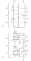
- FIGS. 1A and 1B show a cross-sectional configuration of the semiconductor device according to the first embodiment of the present invention.
- FIG. 1A is a cross-sectional view in the gate length direction (L direction).
- FIG. 1B is a cross-sectional view in the gate width direction (W direction).
- 2A to 2D are cross-sectional views showing respective steps of the method for manufacturing the semiconductor device according to the first embodiment of the present invention.
- FIGS. 2A and 2C are cross-sectional views in the L direction.
- FIGS. 2B and 2D are cross-sectional views in the W direction.
- FIGS. 3A to 3D are cross-sectional views showing respective steps of the method for manufacturing the semiconductor device according to the first embodiment of the present invention.
- FIGS. 3A and 3C are cross-sectional views in the L direction.
- FIGS. 3B and 3D are cross-sectional views in the W direction.
- 4A to 4D are cross-sectional views showing respective steps of the method of manufacturing the semiconductor device according to the first embodiment of the present invention.
- FIGS. 4A and 4C are cross-sectional views in the L direction.
- FIGS. 4B and 4D are cross-sectional views in the W direction.
- 5A to 5D are cross-sectional views showing respective steps of the method for manufacturing the semiconductor device according to the first embodiment of the present invention.
- FIGS. 5A and 5C are cross-sectional views in the L direction.
- 5B and 5D are cross-sectional views in the W direction.
- FIGS. 6A to 6D are cross-sectional views showing respective steps of the method for manufacturing the semiconductor device according to the first embodiment of the present invention.
- FIGS. 6A and 6C are cross-sectional views in the L direction.
- 6 (b) and 6 (d) are cross-sectional views in the W direction.
- 7A to 7D are cross-sectional views showing respective steps of the method of manufacturing the semiconductor device according to the first embodiment of the present invention.
- FIGS. 7A and 7C are cross-sectional views in the L direction.
- FIGS. 7B and 7D are cross-sectional views in the W direction.
- 8A to 8D are cross-sectional views showing respective steps of the method for manufacturing the semiconductor device according to the first embodiment of the present invention.
- FIGS. 8A and 8C are cross-sectional views in the L direction.
- FIGS. 9A and 9B are cross-sectional views showing respective steps of the method for manufacturing the semiconductor device according to the first embodiment of the present invention, and FIG. 9A is a cross-sectional view in the L direction.
- FIG. 9B is a cross-sectional view in the W direction.
- FIGS. 10A and 10B are cross-sectional views showing respective steps of the method for manufacturing the semiconductor device according to the first embodiment of the present invention, and FIG. 10A is a cross-sectional view in the L direction.
- FIG. 10B is a cross-sectional view in the W direction.
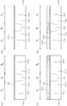
- FIG. 11 is a diagram showing variations in the cross-sectional configuration in the W direction in the semiconductor device according to the first embodiment of the present invention.
- 12A and 12B show a cross-sectional configuration of the semiconductor device according to the second embodiment of the present invention, and FIG. 12A is a cross-sectional view in the L direction, and FIG. Is a cross-sectional view in the W direction.
- FIGS. 13A to 13D are cross-sectional views showing respective steps of the method of manufacturing a semiconductor device according to the second embodiment of the present invention, and FIGS. 13A and 13C are cross-sections in the L direction.
- FIGS. 13B and 13D are cross-sectional views in the W direction.
- FIGS. 14 (a) to 14 (d) are cross-sectional views showing respective steps of the method of manufacturing a semiconductor device according to the second embodiment of the present invention, and FIGS. 14 (a) and 14 (c) are cross-sections in the L direction.
- 14 (b) and 14 (d) are cross-sectional views in the W direction.
- 15 (a) to 15 (d) are cross-sectional views showing respective steps of the method of manufacturing a semiconductor device according to the second embodiment of the present invention, and FIGS. 15 (a) and 15 (c) are cross-sections in the L direction.
- FIGS. 15B and 15D are cross-sectional views in the W direction.
- FIG. 16 is a diagram showing variations in the cross-sectional configuration in the W direction in the semiconductor device according to the second embodiment of the present invention.
- 1 is a cross-sectional view of a semiconductor device including a MIPS-structured DMG disclosed in Non-Patent Document 1.
- FIG. 1A and 1B show a cross-sectional configuration of the semiconductor device according to the first embodiment of the present invention.
- FIG. 1A is a cross-sectional view in the gate length direction (L direction).
- FIG. 1B is a cross-sectional view in the gate width direction (W direction).
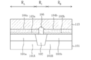
- R A shown on the left side indicates an NMIS formation region where the NMIS transistor is formed
- R B shown on the right side indicates a PMIS formation region where the PMIS transistor is formed
- “R C ” indicates an element isolation formation region in which an element isolation region is formed.
- An element isolation region 102 made of STI is formed to partition the second active region 101B made of the semiconductor substrate 101.
- a first gate electrode 122a is formed on the first active region 101A through a first gate insulating film 103a, and a second gate insulating film 103b is formed on the second active region 101B. Thus, a second gate electrode 122b is formed.
- the gate insulating films 103a and 103b are made of, for example, an HfSiO film that is a high-k film.
- the first gate electrode 122a of the NMIS transistor includes a first metal-containing conductive film 104a formed on the first gate insulating film 103a and a third metal formed on the first metal-containing conductive film 104a.
- the second gate electrode 122b of the PMIS transistor is composed of a second metal-containing conductive film 104b formed on the second gate insulating film 103b and a second metal-containing conductive film. And a third metal-containing conductive film 113 formed on the film 104b.
- the first metal-containing conductive film 104a is made of, for example, a material including at least one of a Ta compound and an Hf compound
- the second metal-containing conductive film 104b is, for example, at least of a Ti compound and a Ru compound.
- the third metal-containing conductive film 113 is made of, for example, a silicide containing Ti, Ni, Co, or Pt.
- an insulating sidewall spacer 109 is formed on each side surface of the gate electrodes 122a and 122b with an insulating offset spacer 107 interposed therebetween.
- An N-type extension region (shallow N-type source / drain region) 108a is formed below the insulating sidewall spacer 109 in the surface portion of the first active region 101A, and an N-type source / drain is formed outside the N-type extension region (shallow N-type source / drain region).
- a region (deep N-type source / drain region) 110a is formed.
- a P-type extension region (shallow P-type source / drain region) 108b is formed below the insulating sidewall spacer 109 on the surface portion of the second active region 101B, and a P-type source / drain is formed outside the P-type extension region (shallow P-type source / drain region).
- a region (deep P-type source / drain region) 110b is formed.
- Silicide layers 111 are formed on the surface portions of the source / drain regions 110a and 110b.
- An interlayer insulating film 112 is formed on the entire surface of the semiconductor substrate 101 so that the gate electrodes 122a and 122b are buried except for their upper surfaces.
- the upper surface heights of the gate electrodes 122a and 122b are the same as the upper surface height of the interlayer insulating film 112, but they do not necessarily have to be the same height.
- the upper surface height of the gate electrodes 122 a and 122 b may be higher than the upper surface height of the interlayer insulating film 112.
- a feature of the present embodiment is that the third metal-containing conductive film 113 that is a part of each of the gate electrodes 122a and 122b is in contact with each of the first metal-containing conductive film 104a and the second metal-containing conductive film 104b. Thus, it is formed continuously from the first metal-containing conductive film 104a to the second metal-containing conductive film 104b through the element isolation region 102.
- the first metal-containing conductive film 104a constituting the first gate electrode 122a is on and adjacent to the first active region 101A.
- the second metal-containing conductive film 104b that forms the second gate electrode 122b is formed on the end portion of the element isolation region 102 to be formed on the second active region 101B and adjacent to the element isolation region 102. It is formed on the end. That is, in the W direction, the first metal-containing conductive film 104a and the second metal-containing conductive film 104b are formed on the element isolation region 102 located between the first active region 101A and the second active region 101B. Is divided.
- the third metal-containing conductive film 113 fills the space between the first metal-containing conductive film 104a and the second metal-containing conductive film 104b on the element isolation region 102. In other words, it is formed in contact with the element isolation region 102.
- FIGS. 2A and 2C are cross-sectional views illustrating steps of the method for manufacturing a semiconductor device according to FIGS. 2A and 2C, FIGS. 3A and 3C, FIGS.
- FIGS. ), (C), FIG. 6 (a), (c), FIG. 7 (a), (c), FIG. 8 (a), (c), FIG. 9 (a), and FIG. 2 (b), (d), FIG. 3 (b), (d), FIG. 4 (b), (d), FIG. 5 (b), (d), FIG. 6 (b). ), (D), FIG. 7 (b), (d), FIG. 8 (b), (d), FIG. 9 (b), and FIG. 10 (b) are cross-sectional views in the W direction.
- the first active region 101A made of the semiconductor substrate 101 in the NMIS formation region RA and the PMIS formation region R are formed.
- An element isolation region 102 made of STI that partitions the second active region 101B made of the B semiconductor substrate 101 is formed.
- the first active region 101A of the NMIS formation region R A surrounded by the isolation region 102 to form a P-well region 101a, a second of the PMIS formation region R B that is surrounded by the isolation region 102 N well region 101b is formed in active region 101B.
- a first gate insulating film 103a for the NMIS transistor for example, an HfSiO film, which is a high-k film, is formed on the entire surface of the semiconductor substrate 101 by a CVD (chemical vapor deposition) method.
- CVD chemical vapor deposition
- the first gate insulating film 103a for example, at least one of a Ta compound and an Hf compound is used as a metal gate electrode for the NMIS transistor.
- a first metal-containing conductive film 104a having a thickness of about 20 nm is formed from the containing material.
- a first active region 101A and it covers the end portion of the element isolation region 102 adjacent and PMIS formation region R B is a hard mask 105a having a thickness of about 40nm which is open Form.
- the material of the hard mask 105a is preferably a material that does not oxidize a metal material, for example, a Si-based material.
- first gate insulating film 103a and the first metal-containing conductive film 104a wet etching or B It is removed by dry etching.
- the first gate insulating film 103a and the first metal-containing conductive film 104a remain not only on the first active region 101a but also on the end portion of the element isolation region 102 adjacent thereto. Etching is performed. Note that in the case of using dry etching, the first gate insulating film 103a and the first metal-containing conductive film 104a may be continuously etched by changing etching conditions such as an etchant in the same chamber.
- an HfSiO film for example, a high-k film is formed on the entire surface of the semiconductor substrate 101 as a second gate insulating film 103b for the PMIS transistor by a CVD method. Form a film.
- the metal gate electrode for the PMIS transistor for example, at least one of a Ti compound and a Ru compound is formed on the second gate insulating film 103b.
- a second metal-containing conductive film 104b having a thickness of about 20 nm is formed from the containing material.
- the second gate insulating film 103b and the second metal-containing conductive film 104b for the PMIS transistor deposited in the NMIS formation region RA are removed.
- the material of the hard mask 105b is preferably a material that does not oxidize a metal material, for example, a Si-based material.
- the second gate insulating film 103b and the second metal-containing conductive film 104b in the NMIS formation region RA are wet-etched or hardened using the hard mask 105b. It is removed by dry etching. At this time, the hard mask 105a functions as an etching stopper in the NMIS formation region RA . At this time, the second gate insulating film 103b and the second metal-containing conductive film 104b remain not only on the second active region 101B but also on the edge of the element isolation region 102 adjacent thereto. Etching is performed.
- the first metal-containing conductive film 104a and the second metal-containing conductive film 104b are at least predetermined on the element isolation region 102 located between the first active region 101A and the second active region 101B.
- Distance the total thickness of the second gate insulating film 103b and the second metal-containing conductive film 104b or more.
- the second gate insulating film 103b and the second metal-containing conductive film 104b may be continuously etched by changing etching conditions such as an etchant in the same chamber.
- step shown in FIG. 3 (c) and (d) without removing the first gate insulating film 103a of the PMIS formation region R B, which can also be used as a gate insulating film for PMIS transistor there, but in that case, when depositing the second metal-containing conductive film 104b in the step shown in FIG. 4 (c) and (d), the first gate insulating film 103a remaining in PMIS formation region R B Degradation is inevitable. Therefore, in this embodiment, not only a metal gate electrode but also a gate insulating film is separately formed for each transistor.
- a polysilicon film 106 having a thickness of about 100 nm is formed.
- the polysilicon film 106 and the first metal-containing conductive film 104a of the NMIS formation region R A, and the polysilicon film 106 and the in PMIS formation region R B Each of the two metal-containing conductive films 104b is patterned by dry etching.
- the first gate portion 121a composed of the first metal-containing conductive film 104a and the polysilicon film 106 is formed on the first active region 101A via the first gate insulating film 103a
- the second A second gate portion 121b made of the second metal-containing conductive film 104b and the polysilicon film 106 is formed on the active region 101B via the second gate insulating film 103b.
- the polysilicon film 106 of the first gate portion 121a and the polysilicon film 106 of the second gate portion 121b are formed on the element isolation region 102. It is integrally formed through the silicon film 106. Further, in the steps shown in FIGS. 7A and 7B, the first gate insulating film 103a outside the first gate portion 121a and the second gate insulating film 103b outside the second gate portion 121b. Are removed respectively. In the present embodiment, the material and etching conditions of the metal-containing conductive films 104a and 104b are appropriately selected, so that the polysilicon film 106 and the metal-containing conductive films 104a and 104b are continuously formed in the same chamber. Etching is performed, thereby patterning the gate portions 121a and 121b simultaneously.
- the gate portions 121a and 121b and the insulating offset spacer 107 are formed.
- the N-type extension region (shallow N-type source / drain region) 108a and the P-type extension region (shallow P) are used.
- Type source / drain region) 108b is formed.
- an insulating sidewall spacer 109 is formed on each side surface of the gate portions 121a and 121b via an insulating offset spacer 107, and then the gate portions 121a and 121b are formed.
- 121b, the insulating offset spacer 107, and the insulating sidewall spacer 109 are used as masks, and ion implantation is performed on each of the first active region 101A and the second active region 101B.
- a deep N-type source / drain region 110a and a P-type source / drain region (deep P-type source / drain region) 110b are formed.
- the surface portion of the polysilicon film 106 constituting the gate portions 121a and 121b and the surface portions of the source / drain regions 110a and 110b are silicided to form a silicide layer. 111 is formed. Thereby, the resistance of the source / drain regions 110a and 110b can be reduced.
- the silicide layer 111 is not necessarily formed on the surface portion of the polysilicon film 106 constituting the gate portions 121a and 121b.
- an interlayer insulating film 112 having a thickness (for example, 200 nm or more) that can cover the gate portions 121 a and 121 b is formed on the entire surface of the semiconductor substrate 101. Film. Thereafter, as shown in FIGS. 10A and 10B, the interlayer insulating film 112 is exposed by, for example, CMP (chemical mechanical polishing) method until the silicide layer 111 provided on the surface portions of the gate portions 121a and 121b is exposed. Polish. At this time, the silicide layer 111 on the surfaces of the gate portions 121a and 121b is not necessarily left.
- CMP chemical mechanical polishing
- the interlayer insulating film 112 is polished until the surface of the polysilicon film 106 constituting the gate portions 121a and 121b is exposed. Good. Further, when polishing the interlayer insulating film 112, a dry etching method may be used instead of the CMP method.
- a metal film (not shown) made of, for example, Ti, Ni, Co, or Pt, for example, has a thickness of about 100 nm (the polysilicon film 106 can be sufficiently silicided on the gate portions 121a and 121b.
- the polysilicon film 106 constituting the gate portions 121a and 121b is reacted with the metal film, and then the unreacted metal film is removed, and then the heat treatment is performed again.
- a third metal-containing conductive film 113 made of silicide.
- the semiconductor device of the present embodiment shown in FIGS. 1A and 1B that is, the first gate electrode 122a composed of the first metal-containing conductive film 104a and the third metal-containing conductive film 113 is provided.
- a semiconductor device including an NMIS transistor and a PMIS transistor having a second gate electrode 122b made of the second metal-containing conductive film 104b and the third metal-containing conductive film 113 is obtained.
- the polysilicon film 106 is completely silicided so that the first metal-containing conductive film 104a, the second metal-containing conductive film 104b, and the element isolation region 102 are in contact with each other. 3 metal-containing conductive film 113 is formed.
- the polysilicon film 106 is silicided while the silicide layer 111 remains on the surfaces of the gate portions 121a and 121b.
- contacts and wirings electrically connected to the gate electrodes 122a and 122b and the source / drain regions 110a and 110b are formed using a known technique.
- a third metal-containing conductive film 113 which is a part of each of the gate electrodes 122a and 122b, that is, a conductive layer made of a material (silicide) having a lower resistance than polysilicon crosses the element isolation region 102 immediately above each of the gate electrodes 104b. It is formed continuously. Therefore, a wiring that electrically connects the first gate electrode 122a and the second gate electrode 122b, that is, a PN boundary wiring on the element isolation region 102 includes a metal (third metal-containing conductive film 113).
- the resistance of the PN boundary wiring can be reduced without taking measures such as increasing the wiring width of the PN boundary wiring.
- the problem such as disconnection of the silicide due to the current concentration on the silicide on the polysilicon surface in the conventional MIPS structure, that is, the PN boundary portion Problems such as disconnection caused by the high resistance of the wiring can be prevented.
- the third metal-containing conductive film 113 is made of silicide, the structure of the semiconductor device according to the present embodiment can be simplified by siliciding silicon in the MIPS structure. Obtainable.
- the gate insulating film 103a and 103b since separately forms the gate insulating film 103a and 103b not only metal-containing conductive film 104a and 104b becomes the metal gate electrode in each of MIS formation region R A and R B, metal It is possible to prevent the gate insulating films 103a and 103b from being deteriorated when the contained conductive films 104a and 104b are patterned.
- a material containing at least one of a Ta compound and an Hf compound is used as the material of the first metal-containing conductive film 104a constituting the first gate electrode 122a of the NMIS transistor.
- the material is not limited to this, and a material having a work function of 4.55 eV or less may be used.
- a material containing at least one of a Ti compound and a Ru compound is used as the material of the second metal-containing conductive film 104b constituting the second gate electrode 122b of the PMIS transistor.
- the material is not limited to this, and a material having a work function of 4.65 eV or more may be used.
- the polysilicon film 106 is silicided while the silicide layer 111 remains on the surfaces of the gate portions 121a and 121b, and the third metal-containing conductive film 113 is formed.
- the silicide layer 111 on the surfaces of the gate portions 121a and 121b is removed by CMP or etching to expose the surface of the polysilicon film 106, and then the polysilicon film 106 is silicified to include the third metal-containing layer.
- a conductive film 113 may be formed.
- the silicide layer 111 may not be formed on the surfaces of the gate portions 121a and 121b.
- a hard mask is formed on the polysilicon film 106 in the steps shown in FIGS. 6C and 6D, and the hard mask is formed in the polysilicon film in the steps shown in FIGS. 7A and 7B.
- 106, and the like and the silicidation of the surface of the polysilicon film 106 is prevented by the hard mask in the process shown in FIGS. 8C and 8D, and after the hard mask is removed, the polysilicon film is removed.
- the third metal-containing conductive film 113 may be formed by performing silicidation of 106.
- the element isolation region 102 is filled so as to fill the space between the first metal-containing conductive film 104a and the second metal-containing conductive film 104b on the element isolation region 102.
- a third metal-containing conductive film 113 made of silicide was formed so as to be in contact with.
- a polysilicon film is interposed between the element isolation region 102 and the third metal-containing conductive film 113.
- the third metal-containing conductive film 113 may be formed by siliciding the polysilicon film 106 so that part of the film 106 remains.
- the third metal-containing conductive film 113 is in contact with the element isolation region 102 as long as it is continuously formed from directly above the first metal-containing conductive film 104a to immediately above the second metal-containing conductive film 104b. It does not have to be.
- the polysilicon film 106 that fills the space between the first metal-containing conductive film 104a and the second metal-containing conductive film 104b on the element isolation region 102 may not be silicided.
- FIG. 12A and 12B show a cross-sectional configuration of the semiconductor device according to the second embodiment of the present invention, and FIG. 12A is a cross-sectional view in the gate length direction (L direction).
- FIG. 12B is a cross-sectional view in the gate width direction (W direction).
- FIG 12 (a) and 12 (b) the the isolation formation region R C of the semiconductor substrate 101, a first active region 101A and PMIS formation region R B comprising a semiconductor substrate 101 of the NMIS formation region R A
- An element isolation region 102 made of STI is formed to partition the second active region 101B made of the semiconductor substrate 101.
- P well region 101a With the first active region 101A of the NMIS formation region surrounded by the isolation region 102 R A are formed P well region 101a, surrounded by the isolation region 102 PMIS formation region a second of R B An N well region 101b is formed in the active region 101B.
- a first gate electrode 132a is formed on the first active region 101A through a first gate insulating film 103a, and a second gate insulating film 103b is formed on the second active region 101B. Thus, a second gate electrode 132b is formed.
- the gate insulating films 103a and 103b are made of, for example, an HfSiO film that is a high-k film.
- the first gate electrode 132a of the NMIS transistor includes a first metal-containing conductive film 104a formed on the first gate insulating film 103a and a third metal formed on the first metal-containing conductive film 104a.
- the film includes a conductive film 104 c, a polysilicon film 106 formed on the third metal-containing conductive film 104 c, and a silicide layer 111 formed on the surface of the polysilicon film 106.
- the second gate electrode 132b of the PMIS transistor includes a second metal-containing conductive film 104b formed on the second gate insulating film 103b and a third metal formed on the second metal-containing conductive film 104b.
- the film includes a conductive film 104 c, a polysilicon film 106 formed on the third metal-containing conductive film 104 c, and a silicide layer 111 formed on the surface of the polysilicon film 106.
- the first metal-containing conductive film 104a is made of a material containing at least one of a Ta compound and an Hf compound
- the second metal-containing conductive film 104b is made of, for example, at least one of a Ti compound and a Ru compound. It consists of a material containing one.
- the material of the third metal-containing conductive film 104c is not particularly limited as long as it has a lower resistance than polysilicon.
- the material is the same as that of the first metal-containing conductive film 104a or the second metal-containing conductive film 104b.
- the refractory metal-containing material can be used.
- an insulating sidewall spacer 109 is formed on each side surface of the gate electrodes 132a and 132b with an insulating offset spacer 107 interposed therebetween.
- An N-type extension region (shallow N-type source / drain region) 108a is formed below the insulating sidewall spacer 109 in the surface portion of the first active region 101A, and an N-type source / drain is formed outside the N-type extension region (shallow N-type source / drain region).
- a region (deep N-type source / drain region) 110a is formed.
- a P-type extension region (shallow so-P-type source / drain region) 108b is formed below the insulating sidewall spacer 109 on the surface of the second active region 101B, and on the outside thereof, a P-type source.
- a drain region (deep P-type source / drain region) 110b is formed.
- Silicide layers 111 are formed on the surface portions of the source / drain regions 110a and 110b.
- An interlayer insulating film 112 is formed on the entire surface of the semiconductor substrate 101 so as to fill the gate electrodes 132a and 132b.
- the third metal-containing conductive film 104c which is a part of each of the gate electrodes 132a and 132b, is the first metal-containing conductive film 104a, the second metal-containing conductive film 104b, and the element isolation region. That is, it is formed continuously from the first metal-containing conductive film 104a through the element isolation region 102 to the second metal-containing conductive film 104b so as to be in contact with each of the first and second metal-containing conductive films 104a.
- the first metal-containing conductive film 104a constituting the first gate electrode 132a is on and adjacent to the first active region 101A.
- the second metal-containing conductive film 104b that forms the second gate electrode 132b is formed on the end portion of the element isolation region 102 to be formed on the second active region 101B and adjacent to the element isolation region 102. It is formed on the end. That is, in the W direction, the first metal-containing conductive film 104 a and the second metal-containing conductive film 104 b are separated on the element isolation region 102.
- the third metal-containing conductive film 104c is recessed in a space between the first metal-containing conductive film 104a and the second metal-containing conductive film 104b on the element isolation region 102.
- the polysilicon film 106 is further formed so as to fill the concave portion.
- FIGS. 13A to 13D, FIGS. 14A to 14D, and FIGS. 15A to 15D show the respective steps of the semiconductor device manufacturing method according to the second embodiment of the present invention.
- 13 (a), (c), FIG. 14 (a), (c) and FIGS. 15 (a), (c) are cross-sectional views in the L direction
- FIG. (D), FIG.14 (b), (d) and FIG.15 (b), (d) are sectional drawings of a W direction.
- the hard masks 105a and 105b are removed as shown in FIGS.
- the first metal-containing conductive film 104a through the first gate insulating film 103a on the first active region 101A of the NMIS formation region R A is formed
- a second metal-containing conductive film 104b is formed on the active region 101B through a second gate insulating film 103b.
- polysilicon film 106 of R B, a third metal-containing conductive film 104c and the second metal-containing conductive film 104b respectively are patterned by dry etching.
- the portion 131a is formed, and the second metal-containing conductive film 104b, the third metal-containing dielectric film 104c, and the polysilicon film 106 are formed on the second active region 101B via the second gate insulating film 103b.
- a second gate portion 131b is formed.
- the third metal-containing dielectric film 104c and the polysilicon film 106 constituting the first gate portion 121a and the third metal constituting the second gate portion 121b.
- the contained dielectric film 104 c and the polysilicon film 106 are integrally formed via the third metal-containing dielectric film 104 c and the polysilicon film 106 formed on the element isolation region 102. Further, in the steps shown in FIGS.
- the first gate insulating film 103a outside the first gate portion 131a and the second gate insulating film 103b outside the second gate portion 131b. are removed respectively.
- the polysilicon film 106, the third metal-containing conductive film 104c, and the first and first conductive films 104a and 104b are appropriately selected in the same chamber by appropriately selecting the material and etching conditions of the metal-containing conductive films 104a and 104b. Etching is continuously performed on the second metal-containing conductive films 104a and 104b, thereby patterning the gate portions 131a and 131b at the same time.
- the first gate portions 131a and 131b and the insulating offset spacers are formed.
- the spacer 107 is used as a mask, ion implantation is performed on each of the first active region 101A and the second active region 101B to thereby form an N-type extension region (shallow N-type source / drain region) 108a and a P-type extension region. (Shallow P-type source / drain region) 108b is formed.
- an insulating sidewall spacer 109 is formed on each side surface of the gate portions 131a and 131b via an insulating offset spacer 107, and then the gate portion 131a. And 131b, and the insulating offset spacer 107 and the insulating sidewall spacer 109 as a mask, ion implantation is performed on each of the first active region 101A and the second active region 101B to thereby form an N-type source / drain region. (Deep N-type source / drain regions) 110a and P-type source / drain regions (deep P-type source / drain regions) 110b are formed.
- the surface portion of the polysilicon film 106 constituting the gate portions 131a and 131b and the surface portions of the source / drain regions 110a and 110b are silicided to form a silicide layer.
- 111 is formed.
- the first gate electrode 132a and the second gate electrode 132b in which the silicide layer 111 is formed on the polysilicon film 106 are formed, and the gate electrodes 132a and 132b and the source / drain regions 110a and 110b are lowered. It can be made resistant.
- an interlayer insulating film 112 having a thickness (for example, a thickness of 200 nm or more) that can cover the gate electrodes 132a and 132b is formed on the entire surface of the semiconductor substrate 101.
- a thickness for example, a thickness of 200 nm or more
- the semiconductor device of this embodiment shown in FIGS. 12A and 12B that is, from the first metal-containing conductive film 104a, the third metal-containing conductive film 104c, the polysilicon film 106, and the silicide layer 111.
- a semiconductor device including a transistor is obtained.
- contacts and wirings that are electrically connected to the gate electrodes 132a and 132b and the source / drain regions 110a and 110b are formed using a known technique.
- the resistance of the PN boundary wiring can be reduced without taking measures such as increasing the wiring width of the PN boundary wiring.
- a problem such as disconnection of the silicide due to current concentration on the silicide on the polysilicon surface in the conventional MIPS structure, that is, a PN boundary portion Problems such as disconnection caused by the high resistance of the wiring can be prevented.
- the first metal-containing conductive film 104a constituting the first gate electrode 132a and the second metal-containing conductive film 104b constituting the second gate electrode 132b are directly above.
- the third metal-containing conductive film 104c so as to be in contact with the element isolation region 102, the structure of the semiconductor device according to this embodiment can be easily obtained.
- the polysilicon film 106 that is a part of each of the first gate electrode 132a and the second gate electrode 132b is further formed on the third metal-containing conductive film 104c. Therefore, the structure of the semiconductor device according to the present embodiment can be easily obtained by inserting another metal between the metal and silicon in the MIPS structure.
- the gate insulating film 103a and 103b since separately forms the gate insulating film 103a and 103b not only metal-containing conductive film 104a and 104b becomes the metal gate electrode in each of MIS formation region R A and R B, metal It is possible to prevent the gate insulating films 103a and 103b from being deteriorated when the contained conductive films 104a and 104b are patterned.
- a material containing at least one of a Ta compound and an Hf compound is used as the material of the first metal-containing conductive film 104a constituting the first gate electrode 132a of the NMIS transistor.
- the material is not limited to this, and a material having a work function of 4.55 eV or less may be used.
- a material containing at least one of a Ti compound and a Ru compound is used as the material of the second metal-containing conductive film 104b constituting the second gate electrode 132b of the PMIS transistor.
- the material is not limited to this, and a material having a work function of 4.65 eV or more may be used.
- the polysilicon constituting the gate electrodes 132a and 132b is formed. Only the surface portion of the film 106 is silicided to form a silicide layer 111. However, instead of this, the polysilicon film 106 may be completely silicided.
- the third metal-containing conductive film 104c is placed in a space between the first metal-containing conductive film 104a and the second metal-containing conductive film 104b on the element isolation region 102. It was formed relatively thin so that the concave portion remained. However, instead of this, as shown in FIG. 16 (variation of the cross-sectional configuration in the W direction in the semiconductor device of the present embodiment), the third metal-containing conductive film 104c is replaced with the first metal on the element isolation region 102. You may form comparatively thickly so that the space pinched
Landscapes
- Metal-Oxide And Bipolar Metal-Oxide Semiconductor Integrated Circuits (AREA)
- Electrodes Of Semiconductors (AREA)
- Insulated Gate Type Field-Effect Transistor (AREA)
Priority Applications (1)
| Application Number | Priority Date | Filing Date | Title |
|---|---|---|---|
| US12/619,222 US8350332B2 (en) | 2008-03-14 | 2009-11-16 | Semiconductor device and method of manufacturing the same |
Applications Claiming Priority (2)
| Application Number | Priority Date | Filing Date | Title |
|---|---|---|---|
| JP2008066543A JP2009224509A (ja) | 2008-03-14 | 2008-03-14 | 半導体装置及びその製造方法 |
| JP2008-066543 | 2008-03-14 |
Related Child Applications (1)
| Application Number | Title | Priority Date | Filing Date |
|---|---|---|---|
| US12/619,222 Continuation US8350332B2 (en) | 2008-03-14 | 2009-11-16 | Semiconductor device and method of manufacturing the same |
Publications (1)
| Publication Number | Publication Date |
|---|---|
| WO2009113227A1 true WO2009113227A1 (ja) | 2009-09-17 |
Family
ID=41064901
Family Applications (1)
| Application Number | Title | Priority Date | Filing Date |
|---|---|---|---|
| PCT/JP2009/000184 Ceased WO2009113227A1 (ja) | 2008-03-14 | 2009-01-20 | 半導体装置及びその製造方法 |
Country Status (3)
| Country | Link |
|---|---|
| US (1) | US8350332B2 (https=) |
| JP (1) | JP2009224509A (https=) |
| WO (1) | WO2009113227A1 (https=) |
Families Citing this family (6)
| Publication number | Priority date | Publication date | Assignee | Title |
|---|---|---|---|---|
| JP5349903B2 (ja) * | 2008-02-28 | 2013-11-20 | ルネサスエレクトロニクス株式会社 | 半導体装置の製造方法および半導体装置 |
| US9070784B2 (en) | 2011-07-22 | 2015-06-30 | Taiwan Semiconductor Manufacturing Company, Ltd. | Metal gate structure of a CMOS semiconductor device and method of forming the same |
| US9041116B2 (en) | 2012-05-23 | 2015-05-26 | International Business Machines Corporation | Structure and method to modulate threshold voltage for high-K metal gate field effect transistors (FETs) |
| US9401311B2 (en) * | 2014-05-02 | 2016-07-26 | International Business Machines Corporation | Self aligned structure and method for high-K metal gate work function tuning |
| US9818746B2 (en) * | 2016-01-13 | 2017-11-14 | International Business Machines Corporation | Structure and method to suppress work function effect by patterning boundary proximity in replacement metal gate |
| US11018139B2 (en) * | 2019-08-13 | 2021-05-25 | Micron Technology, Inc. | Integrated transistors and methods of forming integrated transistors |
Citations (3)
| Publication number | Priority date | Publication date | Assignee | Title |
|---|---|---|---|---|
| WO2001071807A1 (en) * | 2000-03-24 | 2001-09-27 | Fujitsu Limited | Semiconductor device and method of manufacture thereof |
| JP2007184583A (ja) * | 2005-12-30 | 2007-07-19 | Internatl Business Mach Corp <Ibm> | 高性能cmos回路及びその製造方法 |
| JP2008034751A (ja) * | 2006-07-31 | 2008-02-14 | Fujitsu Ltd | 半導体装置及びその製造方法 |
Family Cites Families (9)
| Publication number | Priority date | Publication date | Assignee | Title |
|---|---|---|---|---|
| US7183182B2 (en) * | 2003-09-24 | 2007-02-27 | International Business Machines Corporation | Method and apparatus for fabricating CMOS field effect transistors |
| US7148546B2 (en) * | 2003-09-30 | 2006-12-12 | Texas Instruments Incorporated | MOS transistor gates with doped silicide and methods for making the same |
| JP4151976B2 (ja) | 2005-02-25 | 2008-09-17 | 株式会社東芝 | 半導体装置 |
| JP2007019396A (ja) | 2005-07-11 | 2007-01-25 | Renesas Technology Corp | Mos構造を有する半導体装置およびその製造方法 |
| JP2007134456A (ja) | 2005-11-09 | 2007-05-31 | Toshiba Corp | 半導体装置の製造方法 |
| JP2007335512A (ja) | 2006-06-13 | 2007-12-27 | Renesas Technology Corp | 半導体装置及びその製造方法 |
| US20080017936A1 (en) * | 2006-06-29 | 2008-01-24 | International Business Machines Corporation | Semiconductor device structures (gate stacks) with charge compositions |
| JP2008016538A (ja) * | 2006-07-04 | 2008-01-24 | Renesas Technology Corp | Mos構造を有する半導体装置及びその製造方法 |
| US20090039441A1 (en) * | 2007-08-10 | 2009-02-12 | Hongfa Luna | Mosfet with metal gate electrode |
-
2008
- 2008-03-14 JP JP2008066543A patent/JP2009224509A/ja active Pending
-
2009
- 2009-01-20 WO PCT/JP2009/000184 patent/WO2009113227A1/ja not_active Ceased
- 2009-11-16 US US12/619,222 patent/US8350332B2/en not_active Expired - Fee Related
Patent Citations (3)
| Publication number | Priority date | Publication date | Assignee | Title |
|---|---|---|---|---|
| WO2001071807A1 (en) * | 2000-03-24 | 2001-09-27 | Fujitsu Limited | Semiconductor device and method of manufacture thereof |
| JP2007184583A (ja) * | 2005-12-30 | 2007-07-19 | Internatl Business Mach Corp <Ibm> | 高性能cmos回路及びその製造方法 |
| JP2008034751A (ja) * | 2006-07-31 | 2008-02-14 | Fujitsu Ltd | 半導体装置及びその製造方法 |
Also Published As
| Publication number | Publication date |
|---|---|
| US20100059827A1 (en) | 2010-03-11 |
| US8350332B2 (en) | 2013-01-08 |
| JP2009224509A (ja) | 2009-10-01 |
Similar Documents
| Publication | Publication Date | Title |
|---|---|---|
| US9607892B2 (en) | Method for forming a two-layered hard mask on top of a gate structure | |
| US8592271B2 (en) | Metal-gate CMOS device and fabrication method thereof | |
| JP3793190B2 (ja) | 半導体装置の製造方法 | |
| CN101345244B (zh) | 半导体装置及其制造方法 | |
| US8420473B2 (en) | Replacement gate devices with barrier metal for simultaneous processing | |
| CN100573873C (zh) | 半导体器件及其制造方法 | |
| JP4299791B2 (ja) | Cmosデバイスのゲート構造を作製する方法 | |
| JP2009135419A (ja) | 半導体装置及びその製造方法 | |
| CN100539150C (zh) | 半导体装置制造方法 | |
| JP2009141168A (ja) | 半導体装置及びその製造方法 | |
| JP2009194352A (ja) | 半導体装置の製造方法 | |
| US6468851B1 (en) | Method of fabricating CMOS device with dual gate electrode | |
| JP4181537B2 (ja) | 半導体装置およびその製造方法 | |
| JP2009283497A (ja) | 半導体装置及び半導体装置の製造方法 | |
| WO2009113227A1 (ja) | 半導体装置及びその製造方法 | |
| US9548239B2 (en) | Method for fabricating contact plug in an interlayer dielectric layer | |
| JP2009267118A (ja) | 半導体装置の製造方法および半導体装置 | |
| JP5410398B2 (ja) | 半導体装置 | |
| JP5011196B2 (ja) | 半導体装置およびその製造方法 | |
| JP6731344B2 (ja) | ハイブリッドの高−k first及び高−k lastリプレースメントゲートプロセス | |
| JP2007165558A (ja) | 半導体装置およびその製造方法 | |
| CN101165896A (zh) | 半导体装置及其制造方法 | |
| JP2008034413A (ja) | 半導体装置及びその製造方法 | |
| JP4958408B2 (ja) | 半導体装置 | |
| JP2010010507A (ja) | 半導体装置およびその製造方法 |
Legal Events
| Date | Code | Title | Description |
|---|---|---|---|
| 121 | Ep: the epo has been informed by wipo that ep was designated in this application |
Ref document number: 09720187 Country of ref document: EP Kind code of ref document: A1 |
|
| NENP | Non-entry into the national phase |
Ref country code: DE |
|
| 122 | Ep: pct application non-entry in european phase |
Ref document number: 09720187 Country of ref document: EP Kind code of ref document: A1 |