WO2009113227A1 - Semiconductor device and manufacturing method thereof - Google Patents
Semiconductor device and manufacturing method thereof Download PDFInfo
- Publication number
- WO2009113227A1 WO2009113227A1 PCT/JP2009/000184 JP2009000184W WO2009113227A1 WO 2009113227 A1 WO2009113227 A1 WO 2009113227A1 JP 2009000184 W JP2009000184 W JP 2009000184W WO 2009113227 A1 WO2009113227 A1 WO 2009113227A1
- Authority
- WO
- WIPO (PCT)
- Prior art keywords
- metal
- conductive film
- containing conductive
- semiconductor device
- gate electrode
- Prior art date
Links
- 239000004065 semiconductor Substances 0.000 title claims description 137
- 238000004519 manufacturing process Methods 0.000 title claims description 40
- 239000002184 metal Substances 0.000 claims abstract description 305
- 229910052751 metal Inorganic materials 0.000 claims abstract description 305
- 238000002955 isolation Methods 0.000 claims abstract description 88
- 238000000034 method Methods 0.000 claims description 47
- 239000000463 material Substances 0.000 claims description 44
- 229910021332 silicide Inorganic materials 0.000 claims description 39
- FVBUAEGBCNSCDD-UHFFFAOYSA-N silicide(4-) Chemical compound [Si-4] FVBUAEGBCNSCDD-UHFFFAOYSA-N 0.000 claims description 39
- 239000000758 substrate Substances 0.000 claims description 35
- XUIMIQQOPSSXEZ-UHFFFAOYSA-N Silicon Chemical group [Si] XUIMIQQOPSSXEZ-UHFFFAOYSA-N 0.000 claims description 29
- 229910052710 silicon Inorganic materials 0.000 claims description 29
- 239000010703 silicon Substances 0.000 claims description 29
- 150000001875 compounds Chemical class 0.000 claims description 28
- 238000009751 slip forming Methods 0.000 claims description 9
- 238000005192 partition Methods 0.000 claims description 8
- 238000000059 patterning Methods 0.000 claims description 6
- 239000012789 electroconductive film Substances 0.000 abstract 8
- 229910021420 polycrystalline silicon Inorganic materials 0.000 description 64
- 229920005591 polysilicon Polymers 0.000 description 63
- 230000015572 biosynthetic process Effects 0.000 description 50
- 208000011380 COVID-19–associated multisystem inflammatory syndrome in children Diseases 0.000 description 36
- 239000010410 layer Substances 0.000 description 27
- 125000006850 spacer group Chemical group 0.000 description 23
- 238000005530 etching Methods 0.000 description 10
- 230000010354 integration Effects 0.000 description 10
- 239000011229 interlayer Substances 0.000 description 10
- 238000001312 dry etching Methods 0.000 description 7
- 238000005468 ion implantation Methods 0.000 description 6
- 230000002250 progressing effect Effects 0.000 description 5
- 229910004129 HfSiO Inorganic materials 0.000 description 4
- 238000005229 chemical vapour deposition Methods 0.000 description 3
- 230000009977 dual effect Effects 0.000 description 3
- 238000010438 heat treatment Methods 0.000 description 3
- 239000007769 metal material Substances 0.000 description 3
- 229910052814 silicon oxide Inorganic materials 0.000 description 3
- 238000010586 diagram Methods 0.000 description 2
- 238000005498 polishing Methods 0.000 description 2
- 239000003870 refractory metal Substances 0.000 description 2
- 239000002210 silicon-based material Substances 0.000 description 2
- 229910004298 SiO 2 Inorganic materials 0.000 description 1
- VYPSYNLAJGMNEJ-UHFFFAOYSA-N Silicium dioxide Chemical compound O=[Si]=O VYPSYNLAJGMNEJ-UHFFFAOYSA-N 0.000 description 1
- 230000015556 catabolic process Effects 0.000 description 1
- 230000000295 complement effect Effects 0.000 description 1
- 238000006731 degradation reaction Methods 0.000 description 1
- 238000000151 deposition Methods 0.000 description 1
- 239000007772 electrode material Substances 0.000 description 1
- 239000012535 impurity Substances 0.000 description 1
- 239000000126 substance Substances 0.000 description 1
- 238000001039 wet etching Methods 0.000 description 1
Images


Classifications
-
- H—ELECTRICITY
- H01—ELECTRIC ELEMENTS
- H01L—SEMICONDUCTOR DEVICES NOT COVERED BY CLASS H10
- H01L21/00—Processes or apparatus adapted for the manufacture or treatment of semiconductor or solid state devices or of parts thereof
- H01L21/70—Manufacture or treatment of devices consisting of a plurality of solid state components formed in or on a common substrate or of parts thereof; Manufacture of integrated circuit devices or of parts thereof
- H01L21/77—Manufacture or treatment of devices consisting of a plurality of solid state components or integrated circuits formed in, or on, a common substrate
- H01L21/78—Manufacture or treatment of devices consisting of a plurality of solid state components or integrated circuits formed in, or on, a common substrate with subsequent division of the substrate into plural individual devices
- H01L21/82—Manufacture or treatment of devices consisting of a plurality of solid state components or integrated circuits formed in, or on, a common substrate with subsequent division of the substrate into plural individual devices to produce devices, e.g. integrated circuits, each consisting of a plurality of components
- H01L21/822—Manufacture or treatment of devices consisting of a plurality of solid state components or integrated circuits formed in, or on, a common substrate with subsequent division of the substrate into plural individual devices to produce devices, e.g. integrated circuits, each consisting of a plurality of components the substrate being a semiconductor, using silicon technology
- H01L21/8232—Field-effect technology
- H01L21/8234—MIS technology, i.e. integration processes of field effect transistors of the conductor-insulator-semiconductor type
- H01L21/8238—Complementary field-effect transistors, e.g. CMOS
- H01L21/823828—Complementary field-effect transistors, e.g. CMOS with a particular manufacturing method of the gate conductors, e.g. particular materials, shapes
- H01L21/823842—Complementary field-effect transistors, e.g. CMOS with a particular manufacturing method of the gate conductors, e.g. particular materials, shapes gate conductors with different gate conductor materials or different gate conductor implants, e.g. dual gate structures
-
- H—ELECTRICITY
- H01—ELECTRIC ELEMENTS
- H01L—SEMICONDUCTOR DEVICES NOT COVERED BY CLASS H10
- H01L21/00—Processes or apparatus adapted for the manufacture or treatment of semiconductor or solid state devices or of parts thereof
- H01L21/70—Manufacture or treatment of devices consisting of a plurality of solid state components formed in or on a common substrate or of parts thereof; Manufacture of integrated circuit devices or of parts thereof
- H01L21/77—Manufacture or treatment of devices consisting of a plurality of solid state components or integrated circuits formed in, or on, a common substrate
- H01L21/78—Manufacture or treatment of devices consisting of a plurality of solid state components or integrated circuits formed in, or on, a common substrate with subsequent division of the substrate into plural individual devices
- H01L21/82—Manufacture or treatment of devices consisting of a plurality of solid state components or integrated circuits formed in, or on, a common substrate with subsequent division of the substrate into plural individual devices to produce devices, e.g. integrated circuits, each consisting of a plurality of components
- H01L21/822—Manufacture or treatment of devices consisting of a plurality of solid state components or integrated circuits formed in, or on, a common substrate with subsequent division of the substrate into plural individual devices to produce devices, e.g. integrated circuits, each consisting of a plurality of components the substrate being a semiconductor, using silicon technology
- H01L21/8232—Field-effect technology
- H01L21/8234—MIS technology, i.e. integration processes of field effect transistors of the conductor-insulator-semiconductor type
- H01L21/823437—MIS technology, i.e. integration processes of field effect transistors of the conductor-insulator-semiconductor type with a particular manufacturing method of the gate conductors, e.g. particular materials, shapes
- H01L21/82345—MIS technology, i.e. integration processes of field effect transistors of the conductor-insulator-semiconductor type with a particular manufacturing method of the gate conductors, e.g. particular materials, shapes gate conductors with different gate conductor materials or different gate conductor implants, e.g. dual gate structures
-
- H—ELECTRICITY
- H01—ELECTRIC ELEMENTS
- H01L—SEMICONDUCTOR DEVICES NOT COVERED BY CLASS H10
- H01L21/00—Processes or apparatus adapted for the manufacture or treatment of semiconductor or solid state devices or of parts thereof
- H01L21/70—Manufacture or treatment of devices consisting of a plurality of solid state components formed in or on a common substrate or of parts thereof; Manufacture of integrated circuit devices or of parts thereof
- H01L21/77—Manufacture or treatment of devices consisting of a plurality of solid state components or integrated circuits formed in, or on, a common substrate
- H01L21/78—Manufacture or treatment of devices consisting of a plurality of solid state components or integrated circuits formed in, or on, a common substrate with subsequent division of the substrate into plural individual devices
- H01L21/82—Manufacture or treatment of devices consisting of a plurality of solid state components or integrated circuits formed in, or on, a common substrate with subsequent division of the substrate into plural individual devices to produce devices, e.g. integrated circuits, each consisting of a plurality of components
- H01L21/822—Manufacture or treatment of devices consisting of a plurality of solid state components or integrated circuits formed in, or on, a common substrate with subsequent division of the substrate into plural individual devices to produce devices, e.g. integrated circuits, each consisting of a plurality of components the substrate being a semiconductor, using silicon technology
- H01L21/8232—Field-effect technology
- H01L21/8234—MIS technology, i.e. integration processes of field effect transistors of the conductor-insulator-semiconductor type
- H01L21/823481—MIS technology, i.e. integration processes of field effect transistors of the conductor-insulator-semiconductor type isolation region manufacturing related aspects, e.g. to avoid interaction of isolation region with adjacent structure
-
- H—ELECTRICITY
- H01—ELECTRIC ELEMENTS
- H01L—SEMICONDUCTOR DEVICES NOT COVERED BY CLASS H10
- H01L21/00—Processes or apparatus adapted for the manufacture or treatment of semiconductor or solid state devices or of parts thereof
- H01L21/70—Manufacture or treatment of devices consisting of a plurality of solid state components formed in or on a common substrate or of parts thereof; Manufacture of integrated circuit devices or of parts thereof
- H01L21/77—Manufacture or treatment of devices consisting of a plurality of solid state components or integrated circuits formed in, or on, a common substrate
- H01L21/78—Manufacture or treatment of devices consisting of a plurality of solid state components or integrated circuits formed in, or on, a common substrate with subsequent division of the substrate into plural individual devices
- H01L21/82—Manufacture or treatment of devices consisting of a plurality of solid state components or integrated circuits formed in, or on, a common substrate with subsequent division of the substrate into plural individual devices to produce devices, e.g. integrated circuits, each consisting of a plurality of components
- H01L21/822—Manufacture or treatment of devices consisting of a plurality of solid state components or integrated circuits formed in, or on, a common substrate with subsequent division of the substrate into plural individual devices to produce devices, e.g. integrated circuits, each consisting of a plurality of components the substrate being a semiconductor, using silicon technology
- H01L21/8232—Field-effect technology
- H01L21/8234—MIS technology, i.e. integration processes of field effect transistors of the conductor-insulator-semiconductor type
- H01L21/8238—Complementary field-effect transistors, e.g. CMOS
- H01L21/823878—Complementary field-effect transistors, e.g. CMOS isolation region manufacturing related aspects, e.g. to avoid interaction of isolation region with adjacent structure
-
- H—ELECTRICITY
- H01—ELECTRIC ELEMENTS
- H01L—SEMICONDUCTOR DEVICES NOT COVERED BY CLASS H10
- H01L21/00—Processes or apparatus adapted for the manufacture or treatment of semiconductor or solid state devices or of parts thereof
- H01L21/70—Manufacture or treatment of devices consisting of a plurality of solid state components formed in or on a common substrate or of parts thereof; Manufacture of integrated circuit devices or of parts thereof
- H01L21/77—Manufacture or treatment of devices consisting of a plurality of solid state components or integrated circuits formed in, or on, a common substrate
- H01L21/78—Manufacture or treatment of devices consisting of a plurality of solid state components or integrated circuits formed in, or on, a common substrate with subsequent division of the substrate into plural individual devices
- H01L21/82—Manufacture or treatment of devices consisting of a plurality of solid state components or integrated circuits formed in, or on, a common substrate with subsequent division of the substrate into plural individual devices to produce devices, e.g. integrated circuits, each consisting of a plurality of components
- H01L21/822—Manufacture or treatment of devices consisting of a plurality of solid state components or integrated circuits formed in, or on, a common substrate with subsequent division of the substrate into plural individual devices to produce devices, e.g. integrated circuits, each consisting of a plurality of components the substrate being a semiconductor, using silicon technology
- H01L21/8232—Field-effect technology
- H01L21/8234—MIS technology, i.e. integration processes of field effect transistors of the conductor-insulator-semiconductor type
- H01L21/823462—MIS technology, i.e. integration processes of field effect transistors of the conductor-insulator-semiconductor type with a particular manufacturing method of the gate insulating layers, e.g. different gate insulating layer thicknesses, particular gate insulator materials or particular gate insulator implants
-
- H—ELECTRICITY
- H01—ELECTRIC ELEMENTS
- H01L—SEMICONDUCTOR DEVICES NOT COVERED BY CLASS H10
- H01L21/00—Processes or apparatus adapted for the manufacture or treatment of semiconductor or solid state devices or of parts thereof
- H01L21/70—Manufacture or treatment of devices consisting of a plurality of solid state components formed in or on a common substrate or of parts thereof; Manufacture of integrated circuit devices or of parts thereof
- H01L21/77—Manufacture or treatment of devices consisting of a plurality of solid state components or integrated circuits formed in, or on, a common substrate
- H01L21/78—Manufacture or treatment of devices consisting of a plurality of solid state components or integrated circuits formed in, or on, a common substrate with subsequent division of the substrate into plural individual devices
- H01L21/82—Manufacture or treatment of devices consisting of a plurality of solid state components or integrated circuits formed in, or on, a common substrate with subsequent division of the substrate into plural individual devices to produce devices, e.g. integrated circuits, each consisting of a plurality of components
- H01L21/822—Manufacture or treatment of devices consisting of a plurality of solid state components or integrated circuits formed in, or on, a common substrate with subsequent division of the substrate into plural individual devices to produce devices, e.g. integrated circuits, each consisting of a plurality of components the substrate being a semiconductor, using silicon technology
- H01L21/8232—Field-effect technology
- H01L21/8234—MIS technology, i.e. integration processes of field effect transistors of the conductor-insulator-semiconductor type
- H01L21/8238—Complementary field-effect transistors, e.g. CMOS
- H01L21/823857—Complementary field-effect transistors, e.g. CMOS with a particular manufacturing method of the gate insulating layers, e.g. different gate insulating layer thicknesses, particular gate insulator materials or particular gate insulator implants
Definitions
- the present invention relates to a semiconductor device and a manufacturing method thereof, and in particular, in a DMG (Dual Metal Gate) process having a MIPS (Metal / inserted / Poly-Si / Stack) structure, high integration is achieved by increasing a wiring width of a gate electrode or the like.
- the present invention relates to an effective semiconductor manufacturing technique aimed at suppressing an increase in resistance of wiring caused by disconnection or the like at the PN boundary of a metal silicide film without hindering.
- NMIS transistor metal-insulator-semiconductor IV
- N-type transistor P-type MIS transistor
- Metal gate process can be broadly divided into two types: gate first process and gate last process.
- gate first process after forming a gate electrode, a transistor formation process including ion implantation and heat treatment is performed.
- the gate last process a transistor is formed using a dummy gate, and then the dummy gate is removed to form a gate electrode. Therefore, the process is more difficult than the gate first process. Become. For this reason, the formation of a metal gate electrode using a gate-first process is currently being studied.
- CMOS complementary metal-oxide-semiconductor
- Non-Patent Document 1 As described above, application of a high-k gate insulating film and a MIPS-structured DMG is being studied as a next-generation process (see, for example, Non-Patent Document 1).
- FIG. 17 is a cross-sectional view of a semiconductor device including the MIPS-structured DMG disclosed in Non-Patent Document 1, specifically, a cross-sectional view of a transistor in the gate width direction (W direction).
- An element isolation region 2 made of STI (shallow trench isolation) that partitions the two active regions 1B is formed.
- a metal gate electrode 4a is formed on the first active region 1A via a gate insulating film 3a.
- a metal gate electrode 4b is formed on the second active region 1B via a gate insulating film 3b.
- a polysilicon film 6 is continuously formed on the metal gate electrodes 4a and 4b and on the element isolation region 2 located between the electrodes. The polysilicon film 6 is processed into a gate electrode shape including a wiring portion that electrically connects the metal gate electrodes 4a and 4b.
- the surface of the polysilicon film 6 is silicided, whereby a silicide layer 7 is formed.
- impurity regions such as source / drain regions are formed in the MIS formation regions R A and R B by an ion implantation process, a heat treatment process, and the like, thereby forming a transistor structure.
- the wiring that electrically connects the gate electrode of the PMIS transistor and the gate electrode of the NMIS transistor, that is, the PN boundary wiring does not contain metal. Since the region exists, problems such as high resistance and disconnection occur. Specifically, an NMIS metal gate electrode (metal gate electrode 4a) is present in the NMIS formation region, and a PMIS metal gate electrode (metal gate electrode 4b) is present in the PMIS formation region. At the boundary between the MIS formation regions, the NMIS metal and the PMIS metal are removed by the respective patterning processes. As a result, as shown in FIG.
- the silicide layer 7 on the outermost surface of the polysilicon film 6 is formed in the PN boundary wiring (region not including metal). Since the current flows in a concentrated manner, the silicide layer 7 is disconnected or the resistance of the wiring is increased due to the disconnection.
- each of the NMIS metal gate electrode and the PMIS metal gate electrode is directly above.
- the inventors have conceived an invention in which a conductive layer made of a material having a lower resistance than polysilicon is continuously formed.
- a semiconductor device includes a first gate electrode formed on a first active region in a semiconductor substrate and having a first metal-containing conductive film, and a second active in the semiconductor substrate.
- a device isolation formed on the semiconductor substrate so as to partition a second gate electrode formed on the region and having a second metal-containing conductive film, and the first active region and the second active region.
- the first metal-containing conductive film and the second metal-containing conductive film are formed on the element isolation region so as to be separated from each other, and the first metal-containing conductive film
- a third metal-containing conductive film that is a part of each of the first gate electrode and the second gate electrode is continuously formed from the element isolation region to the second metal-containing conductive film.
- the third metal Yushirubedenmaku is in contact with each of the first metal-containing conductive film and the second metal-containing conductive film.
- each gate electrode is directly above each of the first metal-containing conductive film constituting the first gate electrode and the second metal-containing conductive film constituting the second gate electrode.
- a third metal-containing conductive film that is, a conductive layer made of a material having a resistance lower than that of polysilicon is continuously formed so as to cross the element isolation region.
- the wiring that electrically connects the first gate electrode and the second gate electrode, that is, the PN boundary wiring on the element isolation region contains a metal (third metal-containing conductive film). The resistance of the PN boundary wiring can be reduced without taking measures such as increasing the wiring width of the partial wiring.
- the third metal-containing conductive film may be in contact with the element isolation region.
- the third metal-containing conductive film is disposed immediately above the first metal-containing conductive film constituting the first gate electrode and the second metal-containing conductive film constituting the second gate electrode. Is formed so as to be in contact with the element isolation region, the structure of the semiconductor device according to the present invention can be easily obtained.
- the third metal-containing conductive film is formed so as to fill a space between the first metal-containing conductive film and the second metal-containing conductive film on the element isolation region. Also good.
- a silicon region may be interposed between the third metal-containing conductive film and the element isolation region. That is, the portion of the silicon in the MIPS structure directly above the element isolation region may not be silicided.
- the third metal-containing conductive film may be made of silicide.
- the structure of the semiconductor device according to the present invention can be easily obtained by siliciding silicon in the MIPS structure.
- the silicide may contain Ti, Ni, Co, or Pt.
- a silicon film serving as a part of each of the first gate electrode and the second gate electrode may be further formed on the third metal-containing conductive film. That is, the structure of the semiconductor device according to the present invention may be realized by inserting another metal between the metal and silicon in the MIPS structure. The surface of the silicon film may be silicided.
- a first high dielectric constant gate insulating film formed between the first active region and the first gate electrode, the second active region, and the second active region A second high dielectric constant gate insulating film formed between the gate electrode and the gate electrode may be further provided.
- the high dielectric constant gate insulating film means a gate insulating film having a dielectric constant higher than that of SiON, for example, a gate insulating film containing an Hf-based or Zr-based element.
- the first metal-containing conductive film is made of a material having a work function of 4.55 eV or less, for example, It is preferably made of a material containing at least one of a Ta compound and an Hf compound.
- the second metal-containing conductive film is made of a material having a work function of 4.65 eV or more, for example, It is preferably made of a material containing at least one of a Ti compound and a Ru compound.
- the method of manufacturing a semiconductor device includes a step (a) of forming an element isolation region in the semiconductor substrate so as to partition the first active region and the second active region in the semiconductor substrate; A step (b) of forming a first metal-containing conductive film to be a part of the first gate electrode on the first active region; and a part of the second gate electrode on the second active region. A step (c) of forming a second metal-containing conductive film, and from the first metal-containing conductive film through the element isolation region to the second metal-containing conductive film. A third metal-containing conductive film which is a part of each of the first gate electrode and the second gate electrode is continuously in contact with each of the first metal-containing conductive film and the second metal-containing conductive film. (D), and in the step (d), 1 metal-containing conductive film and the second metal-containing conductive film are formed apart from each other in each of the element isolation region.
- the first metal-containing conductive film constituting the first gate electrode and the second metal-containing conductive film constituting the second gate electrode are respectively directly above.
- a third metal-containing conductive film to be a part of each gate electrode, that is, a conductive layer made of a material having a resistance lower than that of polysilicon is continuously formed so as to cross the element isolation region.
- the wiring that electrically connects the first gate electrode and the second gate electrode, that is, the PN boundary wiring on the element isolation region contains a metal (third metal-containing conductive film).
- the resistance of the PN boundary wiring can be reduced without taking measures such as increasing the wiring width of the partial wiring.
- the first metal-containing film on the second active region is formed after forming the first metal-containing conductive film on the semiconductor substrate.
- a step of selectively removing the contained conductive film may be included. In this way, it is possible to prevent the gate insulating film from being deteriorated when the metal-containing conductive film is patterned.
- the step (d) may include a step of forming the third metal-containing conductive film so as to be in contact with the element isolation region.
- the third metal-containing conductive film is disposed immediately above the first metal-containing conductive film constituting the first gate electrode and the second metal-containing conductive film constituting the second gate electrode. Is formed so as to be in contact with the element isolation region, the structure of the semiconductor device according to the present invention can be easily obtained.
- the third metal-containing conductive film has a space sandwiched between the first metal-containing conductive film and the second metal-containing conductive film on the element isolation region.
- a step of forming so as to be buried may be included.
- a silicon film is formed on each of the first metal-containing conductive film, the element isolation region, and the second metal-containing conductive film. Thereafter, the first metal-containing conductive film, the second metal-containing conductive film, and the silicon film were patterned into shapes of the first gate electrode and the second gate electrode, respectively, and then patterned.
- a step of siliciding the silicon film to form the third metal-containing conductive film may be included.
- the step (d) may include a step of leaving a part of the silicon region between the third metal-containing conductive film and the element isolation region. In other words, the portion of the silicon in the MIPS structure that is directly above the element isolation region need not be silicided.
- a part of each of the first gate electrode and the second gate electrode is formed on the third metal-containing conductive film.
- a step (e) of forming a silicon film may be further provided. That is, the structure of the semiconductor device according to the present invention may be realized by inserting another metal between the metal and silicon in the MIPS structure.
- the first metal-containing conductive film, the second metal-containing conductive film, the third metal-containing conductive film, and the silicon film are combined with the first gate electrode and the silicon film.
- the PN boundary wiring that electrically connects the first gate electrode and the second gate electrode contains metal, measures such as increasing the wiring width of the PN boundary wiring are not taken.
- the resistance of the PN boundary wiring can be reduced. Accordingly, it is possible to prevent problems such as disconnection due to an increase in the resistance of the PN boundary wiring while progressing in the high integration in the semiconductor device having the DMG having the MIPS structure.
- FIGS. 1A and 1B show a cross-sectional configuration of the semiconductor device according to the first embodiment of the present invention.
- FIG. 1A is a cross-sectional view in the gate length direction (L direction).
- FIG. 1B is a cross-sectional view in the gate width direction (W direction).
- 2A to 2D are cross-sectional views showing respective steps of the method for manufacturing the semiconductor device according to the first embodiment of the present invention.
- FIGS. 2A and 2C are cross-sectional views in the L direction.
- FIGS. 2B and 2D are cross-sectional views in the W direction.
- FIGS. 3A to 3D are cross-sectional views showing respective steps of the method for manufacturing the semiconductor device according to the first embodiment of the present invention.
- FIGS. 3A and 3C are cross-sectional views in the L direction.
- FIGS. 3B and 3D are cross-sectional views in the W direction.
- 4A to 4D are cross-sectional views showing respective steps of the method of manufacturing the semiconductor device according to the first embodiment of the present invention.
- FIGS. 4A and 4C are cross-sectional views in the L direction.
- FIGS. 4B and 4D are cross-sectional views in the W direction.
- 5A to 5D are cross-sectional views showing respective steps of the method for manufacturing the semiconductor device according to the first embodiment of the present invention.
- FIGS. 5A and 5C are cross-sectional views in the L direction.
- 5B and 5D are cross-sectional views in the W direction.
- FIGS. 6A to 6D are cross-sectional views showing respective steps of the method for manufacturing the semiconductor device according to the first embodiment of the present invention.
- FIGS. 6A and 6C are cross-sectional views in the L direction.
- 6 (b) and 6 (d) are cross-sectional views in the W direction.
- 7A to 7D are cross-sectional views showing respective steps of the method of manufacturing the semiconductor device according to the first embodiment of the present invention.
- FIGS. 7A and 7C are cross-sectional views in the L direction.
- FIGS. 7B and 7D are cross-sectional views in the W direction.
- 8A to 8D are cross-sectional views showing respective steps of the method for manufacturing the semiconductor device according to the first embodiment of the present invention.
- FIGS. 8A and 8C are cross-sectional views in the L direction.
- FIGS. 9A and 9B are cross-sectional views showing respective steps of the method for manufacturing the semiconductor device according to the first embodiment of the present invention, and FIG. 9A is a cross-sectional view in the L direction.
- FIG. 9B is a cross-sectional view in the W direction.
- FIGS. 10A and 10B are cross-sectional views showing respective steps of the method for manufacturing the semiconductor device according to the first embodiment of the present invention, and FIG. 10A is a cross-sectional view in the L direction.
- FIG. 10B is a cross-sectional view in the W direction.
- FIG. 11 is a diagram showing variations in the cross-sectional configuration in the W direction in the semiconductor device according to the first embodiment of the present invention.
- 12A and 12B show a cross-sectional configuration of the semiconductor device according to the second embodiment of the present invention, and FIG. 12A is a cross-sectional view in the L direction, and FIG. Is a cross-sectional view in the W direction.
- FIGS. 13A to 13D are cross-sectional views showing respective steps of the method of manufacturing a semiconductor device according to the second embodiment of the present invention, and FIGS. 13A and 13C are cross-sections in the L direction.
- FIGS. 13B and 13D are cross-sectional views in the W direction.
- FIGS. 14 (a) to 14 (d) are cross-sectional views showing respective steps of the method of manufacturing a semiconductor device according to the second embodiment of the present invention, and FIGS. 14 (a) and 14 (c) are cross-sections in the L direction.
- 14 (b) and 14 (d) are cross-sectional views in the W direction.
- 15 (a) to 15 (d) are cross-sectional views showing respective steps of the method of manufacturing a semiconductor device according to the second embodiment of the present invention, and FIGS. 15 (a) and 15 (c) are cross-sections in the L direction.
- FIGS. 15B and 15D are cross-sectional views in the W direction.
- FIG. 16 is a diagram showing variations in the cross-sectional configuration in the W direction in the semiconductor device according to the second embodiment of the present invention.
- 1 is a cross-sectional view of a semiconductor device including a MIPS-structured DMG disclosed in Non-Patent Document 1.
- FIG. 1A and 1B show a cross-sectional configuration of the semiconductor device according to the first embodiment of the present invention.
- FIG. 1A is a cross-sectional view in the gate length direction (L direction).
- FIG. 1B is a cross-sectional view in the gate width direction (W direction).
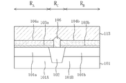
- R A shown on the left side indicates an NMIS formation region where the NMIS transistor is formed
- R B shown on the right side indicates a PMIS formation region where the PMIS transistor is formed
- “R C ” indicates an element isolation formation region in which an element isolation region is formed.
- An element isolation region 102 made of STI is formed to partition the second active region 101B made of the semiconductor substrate 101.
- a first gate electrode 122a is formed on the first active region 101A through a first gate insulating film 103a, and a second gate insulating film 103b is formed on the second active region 101B. Thus, a second gate electrode 122b is formed.
- the gate insulating films 103a and 103b are made of, for example, an HfSiO film that is a high-k film.
- the first gate electrode 122a of the NMIS transistor includes a first metal-containing conductive film 104a formed on the first gate insulating film 103a and a third metal formed on the first metal-containing conductive film 104a.
- the second gate electrode 122b of the PMIS transistor is composed of a second metal-containing conductive film 104b formed on the second gate insulating film 103b and a second metal-containing conductive film. And a third metal-containing conductive film 113 formed on the film 104b.
- the first metal-containing conductive film 104a is made of, for example, a material including at least one of a Ta compound and an Hf compound
- the second metal-containing conductive film 104b is, for example, at least of a Ti compound and a Ru compound.
- the third metal-containing conductive film 113 is made of, for example, a silicide containing Ti, Ni, Co, or Pt.
- an insulating sidewall spacer 109 is formed on each side surface of the gate electrodes 122a and 122b with an insulating offset spacer 107 interposed therebetween.
- An N-type extension region (shallow N-type source / drain region) 108a is formed below the insulating sidewall spacer 109 in the surface portion of the first active region 101A, and an N-type source / drain is formed outside the N-type extension region (shallow N-type source / drain region).
- a region (deep N-type source / drain region) 110a is formed.
- a P-type extension region (shallow P-type source / drain region) 108b is formed below the insulating sidewall spacer 109 on the surface portion of the second active region 101B, and a P-type source / drain is formed outside the P-type extension region (shallow P-type source / drain region).
- a region (deep P-type source / drain region) 110b is formed.
- Silicide layers 111 are formed on the surface portions of the source / drain regions 110a and 110b.
- An interlayer insulating film 112 is formed on the entire surface of the semiconductor substrate 101 so that the gate electrodes 122a and 122b are buried except for their upper surfaces.
- the upper surface heights of the gate electrodes 122a and 122b are the same as the upper surface height of the interlayer insulating film 112, but they do not necessarily have to be the same height.
- the upper surface height of the gate electrodes 122 a and 122 b may be higher than the upper surface height of the interlayer insulating film 112.
- a feature of the present embodiment is that the third metal-containing conductive film 113 that is a part of each of the gate electrodes 122a and 122b is in contact with each of the first metal-containing conductive film 104a and the second metal-containing conductive film 104b. Thus, it is formed continuously from the first metal-containing conductive film 104a to the second metal-containing conductive film 104b through the element isolation region 102.
- the first metal-containing conductive film 104a constituting the first gate electrode 122a is on and adjacent to the first active region 101A.
- the second metal-containing conductive film 104b that forms the second gate electrode 122b is formed on the end portion of the element isolation region 102 to be formed on the second active region 101B and adjacent to the element isolation region 102. It is formed on the end. That is, in the W direction, the first metal-containing conductive film 104a and the second metal-containing conductive film 104b are formed on the element isolation region 102 located between the first active region 101A and the second active region 101B. Is divided.
- the third metal-containing conductive film 113 fills the space between the first metal-containing conductive film 104a and the second metal-containing conductive film 104b on the element isolation region 102. In other words, it is formed in contact with the element isolation region 102.
- FIGS. 2A and 2C are cross-sectional views illustrating steps of the method for manufacturing a semiconductor device according to FIGS. 2A and 2C, FIGS. 3A and 3C, FIGS.
- FIGS. ), (C), FIG. 6 (a), (c), FIG. 7 (a), (c), FIG. 8 (a), (c), FIG. 9 (a), and FIG. 2 (b), (d), FIG. 3 (b), (d), FIG. 4 (b), (d), FIG. 5 (b), (d), FIG. 6 (b). ), (D), FIG. 7 (b), (d), FIG. 8 (b), (d), FIG. 9 (b), and FIG. 10 (b) are cross-sectional views in the W direction.
- the first active region 101A made of the semiconductor substrate 101 in the NMIS formation region RA and the PMIS formation region R are formed.
- An element isolation region 102 made of STI that partitions the second active region 101B made of the B semiconductor substrate 101 is formed.
- the first active region 101A of the NMIS formation region R A surrounded by the isolation region 102 to form a P-well region 101a, a second of the PMIS formation region R B that is surrounded by the isolation region 102 N well region 101b is formed in active region 101B.
- a first gate insulating film 103a for the NMIS transistor for example, an HfSiO film, which is a high-k film, is formed on the entire surface of the semiconductor substrate 101 by a CVD (chemical vapor deposition) method.
- CVD chemical vapor deposition
- the first gate insulating film 103a for example, at least one of a Ta compound and an Hf compound is used as a metal gate electrode for the NMIS transistor.
- a first metal-containing conductive film 104a having a thickness of about 20 nm is formed from the containing material.
- a first active region 101A and it covers the end portion of the element isolation region 102 adjacent and PMIS formation region R B is a hard mask 105a having a thickness of about 40nm which is open Form.
- the material of the hard mask 105a is preferably a material that does not oxidize a metal material, for example, a Si-based material.
- first gate insulating film 103a and the first metal-containing conductive film 104a wet etching or B It is removed by dry etching.
- the first gate insulating film 103a and the first metal-containing conductive film 104a remain not only on the first active region 101a but also on the end portion of the element isolation region 102 adjacent thereto. Etching is performed. Note that in the case of using dry etching, the first gate insulating film 103a and the first metal-containing conductive film 104a may be continuously etched by changing etching conditions such as an etchant in the same chamber.
- an HfSiO film for example, a high-k film is formed on the entire surface of the semiconductor substrate 101 as a second gate insulating film 103b for the PMIS transistor by a CVD method. Form a film.
- the metal gate electrode for the PMIS transistor for example, at least one of a Ti compound and a Ru compound is formed on the second gate insulating film 103b.
- a second metal-containing conductive film 104b having a thickness of about 20 nm is formed from the containing material.
- the second gate insulating film 103b and the second metal-containing conductive film 104b for the PMIS transistor deposited in the NMIS formation region RA are removed.
- the material of the hard mask 105b is preferably a material that does not oxidize a metal material, for example, a Si-based material.
- the second gate insulating film 103b and the second metal-containing conductive film 104b in the NMIS formation region RA are wet-etched or hardened using the hard mask 105b. It is removed by dry etching. At this time, the hard mask 105a functions as an etching stopper in the NMIS formation region RA . At this time, the second gate insulating film 103b and the second metal-containing conductive film 104b remain not only on the second active region 101B but also on the edge of the element isolation region 102 adjacent thereto. Etching is performed.
- the first metal-containing conductive film 104a and the second metal-containing conductive film 104b are at least predetermined on the element isolation region 102 located between the first active region 101A and the second active region 101B.
- Distance the total thickness of the second gate insulating film 103b and the second metal-containing conductive film 104b or more.
- the second gate insulating film 103b and the second metal-containing conductive film 104b may be continuously etched by changing etching conditions such as an etchant in the same chamber.
- step shown in FIG. 3 (c) and (d) without removing the first gate insulating film 103a of the PMIS formation region R B, which can also be used as a gate insulating film for PMIS transistor there, but in that case, when depositing the second metal-containing conductive film 104b in the step shown in FIG. 4 (c) and (d), the first gate insulating film 103a remaining in PMIS formation region R B Degradation is inevitable. Therefore, in this embodiment, not only a metal gate electrode but also a gate insulating film is separately formed for each transistor.
- a polysilicon film 106 having a thickness of about 100 nm is formed.
- the polysilicon film 106 and the first metal-containing conductive film 104a of the NMIS formation region R A, and the polysilicon film 106 and the in PMIS formation region R B Each of the two metal-containing conductive films 104b is patterned by dry etching.
- the first gate portion 121a composed of the first metal-containing conductive film 104a and the polysilicon film 106 is formed on the first active region 101A via the first gate insulating film 103a
- the second A second gate portion 121b made of the second metal-containing conductive film 104b and the polysilicon film 106 is formed on the active region 101B via the second gate insulating film 103b.
- the polysilicon film 106 of the first gate portion 121a and the polysilicon film 106 of the second gate portion 121b are formed on the element isolation region 102. It is integrally formed through the silicon film 106. Further, in the steps shown in FIGS. 7A and 7B, the first gate insulating film 103a outside the first gate portion 121a and the second gate insulating film 103b outside the second gate portion 121b. Are removed respectively. In the present embodiment, the material and etching conditions of the metal-containing conductive films 104a and 104b are appropriately selected, so that the polysilicon film 106 and the metal-containing conductive films 104a and 104b are continuously formed in the same chamber. Etching is performed, thereby patterning the gate portions 121a and 121b simultaneously.
- the gate portions 121a and 121b and the insulating offset spacer 107 are formed.
- the N-type extension region (shallow N-type source / drain region) 108a and the P-type extension region (shallow P) are used.
- Type source / drain region) 108b is formed.
- an insulating sidewall spacer 109 is formed on each side surface of the gate portions 121a and 121b via an insulating offset spacer 107, and then the gate portions 121a and 121b are formed.
- 121b, the insulating offset spacer 107, and the insulating sidewall spacer 109 are used as masks, and ion implantation is performed on each of the first active region 101A and the second active region 101B.
- a deep N-type source / drain region 110a and a P-type source / drain region (deep P-type source / drain region) 110b are formed.
- the surface portion of the polysilicon film 106 constituting the gate portions 121a and 121b and the surface portions of the source / drain regions 110a and 110b are silicided to form a silicide layer. 111 is formed. Thereby, the resistance of the source / drain regions 110a and 110b can be reduced.
- the silicide layer 111 is not necessarily formed on the surface portion of the polysilicon film 106 constituting the gate portions 121a and 121b.
- an interlayer insulating film 112 having a thickness (for example, 200 nm or more) that can cover the gate portions 121 a and 121 b is formed on the entire surface of the semiconductor substrate 101. Film. Thereafter, as shown in FIGS. 10A and 10B, the interlayer insulating film 112 is exposed by, for example, CMP (chemical mechanical polishing) method until the silicide layer 111 provided on the surface portions of the gate portions 121a and 121b is exposed. Polish. At this time, the silicide layer 111 on the surfaces of the gate portions 121a and 121b is not necessarily left.
- CMP chemical mechanical polishing
- the interlayer insulating film 112 is polished until the surface of the polysilicon film 106 constituting the gate portions 121a and 121b is exposed. Good. Further, when polishing the interlayer insulating film 112, a dry etching method may be used instead of the CMP method.
- a metal film (not shown) made of, for example, Ti, Ni, Co, or Pt, for example, has a thickness of about 100 nm (the polysilicon film 106 can be sufficiently silicided on the gate portions 121a and 121b.
- the polysilicon film 106 constituting the gate portions 121a and 121b is reacted with the metal film, and then the unreacted metal film is removed, and then the heat treatment is performed again.
- a third metal-containing conductive film 113 made of silicide.
- the semiconductor device of the present embodiment shown in FIGS. 1A and 1B that is, the first gate electrode 122a composed of the first metal-containing conductive film 104a and the third metal-containing conductive film 113 is provided.
- a semiconductor device including an NMIS transistor and a PMIS transistor having a second gate electrode 122b made of the second metal-containing conductive film 104b and the third metal-containing conductive film 113 is obtained.
- the polysilicon film 106 is completely silicided so that the first metal-containing conductive film 104a, the second metal-containing conductive film 104b, and the element isolation region 102 are in contact with each other. 3 metal-containing conductive film 113 is formed.
- the polysilicon film 106 is silicided while the silicide layer 111 remains on the surfaces of the gate portions 121a and 121b.
- contacts and wirings electrically connected to the gate electrodes 122a and 122b and the source / drain regions 110a and 110b are formed using a known technique.
- a third metal-containing conductive film 113 which is a part of each of the gate electrodes 122a and 122b, that is, a conductive layer made of a material (silicide) having a lower resistance than polysilicon crosses the element isolation region 102 immediately above each of the gate electrodes 104b. It is formed continuously. Therefore, a wiring that electrically connects the first gate electrode 122a and the second gate electrode 122b, that is, a PN boundary wiring on the element isolation region 102 includes a metal (third metal-containing conductive film 113).
- the resistance of the PN boundary wiring can be reduced without taking measures such as increasing the wiring width of the PN boundary wiring.
- the problem such as disconnection of the silicide due to the current concentration on the silicide on the polysilicon surface in the conventional MIPS structure, that is, the PN boundary portion Problems such as disconnection caused by the high resistance of the wiring can be prevented.
- the third metal-containing conductive film 113 is made of silicide, the structure of the semiconductor device according to the present embodiment can be simplified by siliciding silicon in the MIPS structure. Obtainable.
- the gate insulating film 103a and 103b since separately forms the gate insulating film 103a and 103b not only metal-containing conductive film 104a and 104b becomes the metal gate electrode in each of MIS formation region R A and R B, metal It is possible to prevent the gate insulating films 103a and 103b from being deteriorated when the contained conductive films 104a and 104b are patterned.
- a material containing at least one of a Ta compound and an Hf compound is used as the material of the first metal-containing conductive film 104a constituting the first gate electrode 122a of the NMIS transistor.
- the material is not limited to this, and a material having a work function of 4.55 eV or less may be used.
- a material containing at least one of a Ti compound and a Ru compound is used as the material of the second metal-containing conductive film 104b constituting the second gate electrode 122b of the PMIS transistor.
- the material is not limited to this, and a material having a work function of 4.65 eV or more may be used.
- the polysilicon film 106 is silicided while the silicide layer 111 remains on the surfaces of the gate portions 121a and 121b, and the third metal-containing conductive film 113 is formed.
- the silicide layer 111 on the surfaces of the gate portions 121a and 121b is removed by CMP or etching to expose the surface of the polysilicon film 106, and then the polysilicon film 106 is silicified to include the third metal-containing layer.
- a conductive film 113 may be formed.
- the silicide layer 111 may not be formed on the surfaces of the gate portions 121a and 121b.
- a hard mask is formed on the polysilicon film 106 in the steps shown in FIGS. 6C and 6D, and the hard mask is formed in the polysilicon film in the steps shown in FIGS. 7A and 7B.
- 106, and the like and the silicidation of the surface of the polysilicon film 106 is prevented by the hard mask in the process shown in FIGS. 8C and 8D, and after the hard mask is removed, the polysilicon film is removed.
- the third metal-containing conductive film 113 may be formed by performing silicidation of 106.
- the element isolation region 102 is filled so as to fill the space between the first metal-containing conductive film 104a and the second metal-containing conductive film 104b on the element isolation region 102.
- a third metal-containing conductive film 113 made of silicide was formed so as to be in contact with.
- a polysilicon film is interposed between the element isolation region 102 and the third metal-containing conductive film 113.
- the third metal-containing conductive film 113 may be formed by siliciding the polysilicon film 106 so that part of the film 106 remains.
- the third metal-containing conductive film 113 is in contact with the element isolation region 102 as long as it is continuously formed from directly above the first metal-containing conductive film 104a to immediately above the second metal-containing conductive film 104b. It does not have to be.
- the polysilicon film 106 that fills the space between the first metal-containing conductive film 104a and the second metal-containing conductive film 104b on the element isolation region 102 may not be silicided.
- FIG. 12A and 12B show a cross-sectional configuration of the semiconductor device according to the second embodiment of the present invention, and FIG. 12A is a cross-sectional view in the gate length direction (L direction).
- FIG. 12B is a cross-sectional view in the gate width direction (W direction).
- FIG 12 (a) and 12 (b) the the isolation formation region R C of the semiconductor substrate 101, a first active region 101A and PMIS formation region R B comprising a semiconductor substrate 101 of the NMIS formation region R A
- An element isolation region 102 made of STI is formed to partition the second active region 101B made of the semiconductor substrate 101.
- P well region 101a With the first active region 101A of the NMIS formation region surrounded by the isolation region 102 R A are formed P well region 101a, surrounded by the isolation region 102 PMIS formation region a second of R B An N well region 101b is formed in the active region 101B.
- a first gate electrode 132a is formed on the first active region 101A through a first gate insulating film 103a, and a second gate insulating film 103b is formed on the second active region 101B. Thus, a second gate electrode 132b is formed.
- the gate insulating films 103a and 103b are made of, for example, an HfSiO film that is a high-k film.
- the first gate electrode 132a of the NMIS transistor includes a first metal-containing conductive film 104a formed on the first gate insulating film 103a and a third metal formed on the first metal-containing conductive film 104a.
- the film includes a conductive film 104 c, a polysilicon film 106 formed on the third metal-containing conductive film 104 c, and a silicide layer 111 formed on the surface of the polysilicon film 106.
- the second gate electrode 132b of the PMIS transistor includes a second metal-containing conductive film 104b formed on the second gate insulating film 103b and a third metal formed on the second metal-containing conductive film 104b.
- the film includes a conductive film 104 c, a polysilicon film 106 formed on the third metal-containing conductive film 104 c, and a silicide layer 111 formed on the surface of the polysilicon film 106.
- the first metal-containing conductive film 104a is made of a material containing at least one of a Ta compound and an Hf compound
- the second metal-containing conductive film 104b is made of, for example, at least one of a Ti compound and a Ru compound. It consists of a material containing one.
- the material of the third metal-containing conductive film 104c is not particularly limited as long as it has a lower resistance than polysilicon.
- the material is the same as that of the first metal-containing conductive film 104a or the second metal-containing conductive film 104b.
- the refractory metal-containing material can be used.
- an insulating sidewall spacer 109 is formed on each side surface of the gate electrodes 132a and 132b with an insulating offset spacer 107 interposed therebetween.
- An N-type extension region (shallow N-type source / drain region) 108a is formed below the insulating sidewall spacer 109 in the surface portion of the first active region 101A, and an N-type source / drain is formed outside the N-type extension region (shallow N-type source / drain region).
- a region (deep N-type source / drain region) 110a is formed.
- a P-type extension region (shallow so-P-type source / drain region) 108b is formed below the insulating sidewall spacer 109 on the surface of the second active region 101B, and on the outside thereof, a P-type source.
- a drain region (deep P-type source / drain region) 110b is formed.
- Silicide layers 111 are formed on the surface portions of the source / drain regions 110a and 110b.
- An interlayer insulating film 112 is formed on the entire surface of the semiconductor substrate 101 so as to fill the gate electrodes 132a and 132b.
- the third metal-containing conductive film 104c which is a part of each of the gate electrodes 132a and 132b, is the first metal-containing conductive film 104a, the second metal-containing conductive film 104b, and the element isolation region. That is, it is formed continuously from the first metal-containing conductive film 104a through the element isolation region 102 to the second metal-containing conductive film 104b so as to be in contact with each of the first and second metal-containing conductive films 104a.
- the first metal-containing conductive film 104a constituting the first gate electrode 132a is on and adjacent to the first active region 101A.
- the second metal-containing conductive film 104b that forms the second gate electrode 132b is formed on the end portion of the element isolation region 102 to be formed on the second active region 101B and adjacent to the element isolation region 102. It is formed on the end. That is, in the W direction, the first metal-containing conductive film 104 a and the second metal-containing conductive film 104 b are separated on the element isolation region 102.
- the third metal-containing conductive film 104c is recessed in a space between the first metal-containing conductive film 104a and the second metal-containing conductive film 104b on the element isolation region 102.
- the polysilicon film 106 is further formed so as to fill the concave portion.
- FIGS. 13A to 13D, FIGS. 14A to 14D, and FIGS. 15A to 15D show the respective steps of the semiconductor device manufacturing method according to the second embodiment of the present invention.
- 13 (a), (c), FIG. 14 (a), (c) and FIGS. 15 (a), (c) are cross-sectional views in the L direction
- FIG. (D), FIG.14 (b), (d) and FIG.15 (b), (d) are sectional drawings of a W direction.
- the hard masks 105a and 105b are removed as shown in FIGS.
- the first metal-containing conductive film 104a through the first gate insulating film 103a on the first active region 101A of the NMIS formation region R A is formed
- a second metal-containing conductive film 104b is formed on the active region 101B through a second gate insulating film 103b.
- polysilicon film 106 of R B, a third metal-containing conductive film 104c and the second metal-containing conductive film 104b respectively are patterned by dry etching.
- the portion 131a is formed, and the second metal-containing conductive film 104b, the third metal-containing dielectric film 104c, and the polysilicon film 106 are formed on the second active region 101B via the second gate insulating film 103b.
- a second gate portion 131b is formed.
- the third metal-containing dielectric film 104c and the polysilicon film 106 constituting the first gate portion 121a and the third metal constituting the second gate portion 121b.
- the contained dielectric film 104 c and the polysilicon film 106 are integrally formed via the third metal-containing dielectric film 104 c and the polysilicon film 106 formed on the element isolation region 102. Further, in the steps shown in FIGS.
- the first gate insulating film 103a outside the first gate portion 131a and the second gate insulating film 103b outside the second gate portion 131b. are removed respectively.
- the polysilicon film 106, the third metal-containing conductive film 104c, and the first and first conductive films 104a and 104b are appropriately selected in the same chamber by appropriately selecting the material and etching conditions of the metal-containing conductive films 104a and 104b. Etching is continuously performed on the second metal-containing conductive films 104a and 104b, thereby patterning the gate portions 131a and 131b at the same time.
- the first gate portions 131a and 131b and the insulating offset spacers are formed.
- the spacer 107 is used as a mask, ion implantation is performed on each of the first active region 101A and the second active region 101B to thereby form an N-type extension region (shallow N-type source / drain region) 108a and a P-type extension region. (Shallow P-type source / drain region) 108b is formed.
- an insulating sidewall spacer 109 is formed on each side surface of the gate portions 131a and 131b via an insulating offset spacer 107, and then the gate portion 131a. And 131b, and the insulating offset spacer 107 and the insulating sidewall spacer 109 as a mask, ion implantation is performed on each of the first active region 101A and the second active region 101B to thereby form an N-type source / drain region. (Deep N-type source / drain regions) 110a and P-type source / drain regions (deep P-type source / drain regions) 110b are formed.
- the surface portion of the polysilicon film 106 constituting the gate portions 131a and 131b and the surface portions of the source / drain regions 110a and 110b are silicided to form a silicide layer.
- 111 is formed.
- the first gate electrode 132a and the second gate electrode 132b in which the silicide layer 111 is formed on the polysilicon film 106 are formed, and the gate electrodes 132a and 132b and the source / drain regions 110a and 110b are lowered. It can be made resistant.
- an interlayer insulating film 112 having a thickness (for example, a thickness of 200 nm or more) that can cover the gate electrodes 132a and 132b is formed on the entire surface of the semiconductor substrate 101.
- a thickness for example, a thickness of 200 nm or more
- the semiconductor device of this embodiment shown in FIGS. 12A and 12B that is, from the first metal-containing conductive film 104a, the third metal-containing conductive film 104c, the polysilicon film 106, and the silicide layer 111.
- a semiconductor device including a transistor is obtained.
- contacts and wirings that are electrically connected to the gate electrodes 132a and 132b and the source / drain regions 110a and 110b are formed using a known technique.
- the resistance of the PN boundary wiring can be reduced without taking measures such as increasing the wiring width of the PN boundary wiring.
- a problem such as disconnection of the silicide due to current concentration on the silicide on the polysilicon surface in the conventional MIPS structure, that is, a PN boundary portion Problems such as disconnection caused by the high resistance of the wiring can be prevented.
- the first metal-containing conductive film 104a constituting the first gate electrode 132a and the second metal-containing conductive film 104b constituting the second gate electrode 132b are directly above.
- the third metal-containing conductive film 104c so as to be in contact with the element isolation region 102, the structure of the semiconductor device according to this embodiment can be easily obtained.
- the polysilicon film 106 that is a part of each of the first gate electrode 132a and the second gate electrode 132b is further formed on the third metal-containing conductive film 104c. Therefore, the structure of the semiconductor device according to the present embodiment can be easily obtained by inserting another metal between the metal and silicon in the MIPS structure.
- the gate insulating film 103a and 103b since separately forms the gate insulating film 103a and 103b not only metal-containing conductive film 104a and 104b becomes the metal gate electrode in each of MIS formation region R A and R B, metal It is possible to prevent the gate insulating films 103a and 103b from being deteriorated when the contained conductive films 104a and 104b are patterned.
- a material containing at least one of a Ta compound and an Hf compound is used as the material of the first metal-containing conductive film 104a constituting the first gate electrode 132a of the NMIS transistor.
- the material is not limited to this, and a material having a work function of 4.55 eV or less may be used.
- a material containing at least one of a Ti compound and a Ru compound is used as the material of the second metal-containing conductive film 104b constituting the second gate electrode 132b of the PMIS transistor.
- the material is not limited to this, and a material having a work function of 4.65 eV or more may be used.
- the polysilicon constituting the gate electrodes 132a and 132b is formed. Only the surface portion of the film 106 is silicided to form a silicide layer 111. However, instead of this, the polysilicon film 106 may be completely silicided.
- the third metal-containing conductive film 104c is placed in a space between the first metal-containing conductive film 104a and the second metal-containing conductive film 104b on the element isolation region 102. It was formed relatively thin so that the concave portion remained. However, instead of this, as shown in FIG. 16 (variation of the cross-sectional configuration in the W direction in the semiconductor device of the present embodiment), the third metal-containing conductive film 104c is replaced with the first metal on the element isolation region 102. You may form comparatively thickly so that the space pinched
Abstract
A gate electrode (122a) has a first metal-containing electroconductive film (104a) and a third metal-containing electroconductive film (113) formed thereon. A gate electrode (122b) has a second metal-containing electroconductive film (104b) and a third metal-containing electroconductive film (113) formed thereon. The third metal-containing electroconductive film (113) is formed continuously from the first metal-containing electroconductive film (104a) onto the second metal-containing electroconductive film (104b), passing above an element-isolation region (102), so that it is in contact with the first and second metal-containing electroconductive films (104a, 104b).
Description
本発明は、半導体装置及びその製造方法に関し、特にMIPS(Metal inserted Poly-Si Stack)構造のDMG(Dual Metal Gate )プロセスにおいて、ゲート電極等の配線の配線幅を太くする等により高集積化を妨げることなく、金属シリサイド膜のPN境界における断線等に起因する配線の高抵抗化を抑制することを目的とした有効な半導体製造技術に関するものである。
The present invention relates to a semiconductor device and a manufacturing method thereof, and in particular, in a DMG (Dual Metal Gate) process having a MIPS (Metal / inserted / Poly-Si / Stack) structure, high integration is achieved by increasing a wiring width of a gate electrode or the like. The present invention relates to an effective semiconductor manufacturing technique aimed at suppressing an increase in resistance of wiring caused by disconnection or the like at the PN boundary of a metal silicide film without hindering.
近年、半導体装置の高集積化、微細化に伴い、トランジスタにおいても微細化が急速に進められている。これに伴って、トランジスタのゲート絶縁膜においては、薄膜化が進んでいる。ところが、従来のSiO2 やSiONからなるゲート絶縁膜を薄膜化すると、ゲートリーク電流の値が無視できないほど増大してしまう。そこで、ゲート絶縁膜として、高誘電率膜(以下、High-k膜と称する)を用いることが検討されている。比誘電率の高いHigh-k膜をゲート絶縁膜として用いる場合、実際の物理膜厚を厚く確保してトンネル電流を抑えつつ、EOT(等価酸化膜厚)を薄くしてトランジスタの高駆動力化、低消費電力化を実現することができる。
In recent years, with the high integration and miniaturization of semiconductor devices, miniaturization of transistors has been rapidly advanced. Along with this, thinning of the gate insulating film of the transistor is progressing. However, when the conventional gate insulating film made of SiO 2 or SiON is thinned, the value of the gate leakage current increases to a degree that cannot be ignored. Therefore, the use of a high dielectric constant film (hereinafter referred to as “High-k film”) as a gate insulating film has been studied. When using a high-k film with a high relative dielectric constant as the gate insulating film, the actual physical film thickness is kept large to suppress the tunnel current, while the EOT (equivalent oxide film thickness) is thinned to increase the transistor driving capability. , Low power consumption can be realized.
一方、ゲート電極においては、トランジスタの微細化に伴い、電極の空乏化に起因する容量の低下が問題となる。ゲート電極材料として、従来のようにポリシリコンを用いた場合、この容量の低下は、シリコン酸化膜の膜厚に換算して約0.4nmの増大に相当する。この値は、薄膜化が求められているゲート絶縁膜の膜厚と比較すると、無視できない大きさである。そこで、ゲート電極においては、従来のポリシリコンに代えて、メタルを用いることが考えられている。メタルゲート電極を用いる場合、前述のようなゲート空乏化の問題を抑えることができる。しかしながら、High-kゲート絶縁膜にメタルゲート電極を適用するためには、N型MIS(metal-insulator-semiconductor )トランジスタ(以下「NMISトランジスタ」又は「NMIS」と称する)及びP型MISトランジスタ(以下「PMISトランジスタ」又は「PMIS」と称する)のそれぞれについて適切なメタル材料を選定する必要がある。
On the other hand, in the gate electrode, with the miniaturization of the transistor, a decrease in capacitance due to depletion of the electrode becomes a problem. When polysilicon is used as the gate electrode material as in the prior art, this decrease in capacitance corresponds to an increase of about 0.4 nm in terms of the thickness of the silicon oxide film. This value is not negligible compared to the thickness of the gate insulating film that is required to be thin. In view of this, it has been considered to use metal in the gate electrode instead of conventional polysilicon. When the metal gate electrode is used, the above-described problem of gate depletion can be suppressed. However, in order to apply a metal gate electrode to a high-k gate insulating film, an N-type MIS (metal-insulator-semiconductor IV) transistor (hereinafter referred to as “NMIS transistor” or “NMIS”) and a P-type MIS transistor (hereinafter referred to as “N-type transistor”) It is necessary to select an appropriate metal material for each “PMIS transistor” or “PMIS”.
メタルゲートプロセスは、ゲートファーストプロセス及びゲートラストプロセスの2種類に大きく分けることができる。ゲートファーストプロセスにおいては、ゲート電極を形成した後に、イオン注入や熱処理等を含むトランジスタ形成工程を行う。これに対して、ゲートラストプロセスにおいては、ダミーゲートを用いてトランジスタを形成した後に、ダミーゲートを除去してゲート電極を形成するため、ゲートファーストプロセスと比較して、より難易度が高いプロセスとなる。このため、現在、ゲートファーストプロセスを用いたメタルゲート電極形成の検討が行われている。尚、ゲートファーストプロセスにおいては、ゲート加工性やCMOS(complementary-metal-oxide-semiconductor )プロセスとの整合性等を考慮して、一般的にMIPS構造が用いられている。
Metal gate process can be broadly divided into two types: gate first process and gate last process. In the gate first process, after forming a gate electrode, a transistor formation process including ion implantation and heat treatment is performed. In contrast, in the gate last process, a transistor is formed using a dummy gate, and then the dummy gate is removed to form a gate electrode. Therefore, the process is more difficult than the gate first process. Become. For this reason, the formation of a metal gate electrode using a gate-first process is currently being studied. In the gate first process, a MIPS structure is generally used in consideration of gate processability and compatibility with a complementary metal-oxide-semiconductor (CMOS) process.
以上のように、次世代のプロセスとして、High-kゲート絶縁膜とMIPS構造のDMGとを適用することが検討されている(例えば非特許文献1参照)。
As described above, application of a high-k gate insulating film and a MIPS-structured DMG is being studied as a next-generation process (see, for example, Non-Patent Document 1).
図17は、非特許文献1に開示されているMIPS構造のDMGを備えた半導体装置の断面図、具体的には、ゲート幅方向(W方向)のトランジスタの断面図を示す。図17に示すように、半導体基板1における素子分離形成領域RC には、NMIS形成領域RA の半導体基板1からなる第1の活性領域1AとPMIS形成領域RB の半導体基板1からなる第2の活性領域1Bとを区画するSTI(shallow trench isolation)からなる素子分離領域2が形成されている。素子分離領域2に囲まれたNMIS形成領域RA の第1の活性領域1AにはPウェル領域1aが形成されていると共に、素子分離領域2に囲まれたPMIS形成領域RB の第2の活性領域1BにはNウェル領域1bが形成されている。第1の活性領域1A上にはゲート絶縁膜3aを介してメタルゲート電極4aが形成されている。第2の活性領域1B上にはゲート絶縁膜3bを介してメタルゲート電極4bが形成されている。メタルゲート電極4a及び4bの上並びに当該両電極の間に位置する素子分離領域2の上にはポリシリコン膜6が連続的に形成されている。尚、ポリシリコン膜6は、メタルゲート電極4a及び4bを電気的に接続する配線部分を含むゲート電極形状に加工されている。また、ポリシリコン膜6の表面はシリサイド化されており、それによってシリサイド層7が形成されている。また、図示していないが、イオン注入工程や熱処理工程等によって各MIS形成領域RA 及びRB にはソース・ドレイン領域等の不純物領域が形成されており、それによってトランジスタ構造が構成されている。
S.C.Song他、Highly Manufacturable 45nm LSTP CMOSFETs Using Novel Dual High-k and Dual Metal Gate CMOS Integration、VLSI Techonology、2006年8月6日、P.16 FIG. 17 is a cross-sectional view of a semiconductor device including the MIPS-structured DMG disclosed in Non-Patent Document 1, specifically, a cross-sectional view of a transistor in the gate width direction (W direction). As shown in FIG. 17, in the element isolation formation region R C of the semiconductor substrate 1, first made of a semiconductor substrate 1 of the firstactive region 1A and PMIS formation region R B consisting of a semiconductor substrate 1 of the NMIS formation region R A An element isolation region 2 made of STI (shallow trench isolation) that partitions the two active regions 1B is formed. With the first active region 1A of the element isolation region 2 surrounded by NMIS formation region R A are formed P well region 1a, surrounded by the isolation region 2 second of PMIS formation region R B An N well region 1b is formed in the active region 1B. A metal gate electrode 4a is formed on the first active region 1A via a gate insulating film 3a. A metal gate electrode 4b is formed on the second active region 1B via a gate insulating film 3b. A polysilicon film 6 is continuously formed on the metal gate electrodes 4a and 4b and on the element isolation region 2 located between the electrodes. The polysilicon film 6 is processed into a gate electrode shape including a wiring portion that electrically connects the metal gate electrodes 4a and 4b. Further, the surface of the polysilicon film 6 is silicided, whereby a silicide layer 7 is formed. Although not shown, impurity regions such as source / drain regions are formed in the MIS formation regions R A and R B by an ion implantation process, a heat treatment process, and the like, thereby forming a transistor structure. .
SCSong et al., Highly Manufacturable 45nm LSTP CMOSFETs Using Novel Dual High-k and Dual Metal Gate CMOS Integration, VLSI Techonology, August 6, 2006, P.16
S.C.Song他、Highly Manufacturable 45nm LSTP CMOSFETs Using Novel Dual High-k and Dual Metal Gate CMOS Integration、VLSI Techonology、2006年8月6日、P.16 FIG. 17 is a cross-sectional view of a semiconductor device including the MIPS-structured DMG disclosed in Non-Patent Document 1, specifically, a cross-sectional view of a transistor in the gate width direction (W direction). As shown in FIG. 17, in the element isolation formation region R C of the semiconductor substrate 1, first made of a semiconductor substrate 1 of the first
SCSong et al., Highly Manufacturable 45nm LSTP CMOSFETs Using Novel Dual High-k and Dual Metal Gate CMOS Integration, VLSI Techonology, August 6, 2006, P.16
しかしながら、前述の非特許文献1に開示されているMIPS構造のDMGによると、PMISトランジスタのゲート電極とNMISトランジスタのゲート電極とを電気的に接続する配線、つまりPN境界部配線において金属を含まない領域が存在するため、高抵抗化したり、断線したりする等の問題が生じる。具体的には、NMIS形成領域においてはNMIS用のメタルゲート電極(メタルゲート電極4a)が存在し、PMIS形成領域にはPMIS用のメタルゲート電極(メタルゲート電極4b)が存在している一方、当該両MIS形成領域の境界においてはNMIS用のメタルもPMIS用のメタルもそれぞれのパターニング工程によって除去されている。その結果、図17に示すように、電流8は相対的に抵抗の低い箇所を流れるため、PN境界部配線(金属を含まない領域)においては、ポリシリコン膜6の最表面のシリサイド層7に電流が集中して流れるので、シリサイド層7が断線したり、それに起因して配線の高抵抗化が生じたりする。
However, according to the MIPS structure DMG disclosed in Non-Patent Document 1 described above, the wiring that electrically connects the gate electrode of the PMIS transistor and the gate electrode of the NMIS transistor, that is, the PN boundary wiring does not contain metal. Since the region exists, problems such as high resistance and disconnection occur. Specifically, an NMIS metal gate electrode (metal gate electrode 4a) is present in the NMIS formation region, and a PMIS metal gate electrode (metal gate electrode 4b) is present in the PMIS formation region. At the boundary between the MIS formation regions, the NMIS metal and the PMIS metal are removed by the respective patterning processes. As a result, as shown in FIG. 17, since the current 8 flows through a portion having a relatively low resistance, the silicide layer 7 on the outermost surface of the polysilicon film 6 is formed in the PN boundary wiring (region not including metal). Since the current flows in a concentrated manner, the silicide layer 7 is disconnected or the resistance of the wiring is increased due to the disconnection.
尚、前述のような問題を防止するために、従来、PN境界部配線の配線幅を太くする等の対策が取られているが、これは高集積化の妨げとなる。
In addition, in order to prevent the above-described problems, conventionally, measures such as increasing the wiring width of the PN boundary wiring have been taken, but this hinders high integration.
前記に鑑み、本発明は、MIPS構造のDMGを有する半導体装置において高集積化を進展させつつ、PN境界部配線の断線や高抵抗化等の問題を防止できるようにすることを目的とする。
In view of the foregoing, it is an object of the present invention to prevent problems such as disconnection of the PN boundary wiring and high resistance in a semiconductor device having a DMG having a MIPS structure while progressing high integration.
前記の目的を達成するために、本願発明者らは、種々の検討を重ねた結果、MIPS構造のDMGを有する半導体装置において、NMIS用のメタルゲート電極及びPMIS用のメタルゲート電極のそれぞれの直上に、ポリシリコンよりも抵抗が低い材料からなる導電層を連続的に形成するという発明を想到した。
In order to achieve the above object, the present inventors have made various studies and as a result, in a semiconductor device having a DMG having a MIPS structure, each of the NMIS metal gate electrode and the PMIS metal gate electrode is directly above. In addition, the inventors have conceived an invention in which a conductive layer made of a material having a lower resistance than polysilicon is continuously formed.
具体的には、本発明に係る半導体装置は、半導体基板における第1の活性領域上に形成され且つ第1の金属含有導電膜を有する第1のゲート電極と、前記半導体基板における第2の活性領域上に形成され且つ第2の金属含有導電膜を有する第2のゲート電極と、前記第1の活性領域と前記第2の活性領域とを区画するように前記半導体基板に形成された素子分離領域とを備え、前記第1の金属含有導電膜及び前記第2の金属含有導電膜はそれぞれ前記素子分離領域上に互いに離間して形成されており、前記第1の金属含有導電膜上から前記素子分離領域上を経て前記第2の金属含有導電膜の上まで、前記第1のゲート電極及び前記第2のゲート電極のそれぞれの一部となる第3の金属含有導電膜が連続的に形成されており、前記第3の金属含有導電膜は、前記第1の金属含有導電膜及び前記第2の金属含有導電膜のそれぞれと接している。
Specifically, a semiconductor device according to the present invention includes a first gate electrode formed on a first active region in a semiconductor substrate and having a first metal-containing conductive film, and a second active in the semiconductor substrate. A device isolation formed on the semiconductor substrate so as to partition a second gate electrode formed on the region and having a second metal-containing conductive film, and the first active region and the second active region The first metal-containing conductive film and the second metal-containing conductive film are formed on the element isolation region so as to be separated from each other, and the first metal-containing conductive film A third metal-containing conductive film that is a part of each of the first gate electrode and the second gate electrode is continuously formed from the element isolation region to the second metal-containing conductive film. The third metal Yushirubedenmaku is in contact with each of the first metal-containing conductive film and the second metal-containing conductive film.
本発明に係る半導体装置によると、第1のゲート電極を構成する第1の金属含有導電膜、及び第2のゲート電極を構成する第2の金属含有導電膜のそれぞれの直上に、各ゲート電極の一部となる第3の金属含有導電膜、つまりポリシリコンよりも抵抗が低い材料からなる導電層が素子分離領域を横断するように連続的に形成されている。このため、第1のゲート電極と第2のゲート電極とを電気的に接続する配線、つまり素子分離領域上のPN境界部配線が金属(第3の金属含有導電膜)を含むので、PN境界部配線の配線幅を太くする等の対策を講じることなく、PN境界部配線を低抵抗化することができる。これによって、MIPS構造のDMGを有する半導体装置において高集積化を進展させつつ、従来のMIPS構造におけるポリシリコン表面のシリサイドへの電流の集中に起因する当該シリサイドの断線等の問題、つまりPN境界部配線の高抵抗化に起因する断線等の問題を防止することができる。
According to the semiconductor device of the present invention, each gate electrode is directly above each of the first metal-containing conductive film constituting the first gate electrode and the second metal-containing conductive film constituting the second gate electrode. A third metal-containing conductive film, that is, a conductive layer made of a material having a resistance lower than that of polysilicon is continuously formed so as to cross the element isolation region. For this reason, the wiring that electrically connects the first gate electrode and the second gate electrode, that is, the PN boundary wiring on the element isolation region contains a metal (third metal-containing conductive film). The resistance of the PN boundary wiring can be reduced without taking measures such as increasing the wiring width of the partial wiring. As a result, while a high degree of integration is progressing in a semiconductor device having a MIPS structure DMG, a problem such as disconnection of the silicide due to current concentration on the silicide on the polysilicon surface in the conventional MIPS structure, that is, a PN boundary portion Problems such as disconnection caused by the high resistance of the wiring can be prevented.
本発明に係る半導体装置において、前記第3の金属含有導電膜は前記素子分離領域と接していてもよい。このようにすると、第1のゲート電極を構成する第1の金属含有導電膜、及び第2のゲート電極を構成する第2の金属含有導電膜のそれぞれの直上に、第3の金属含有導電膜を素子分離領域と接するように形成することによって、本発明に係る半導体装置の構造を簡単に得ることができる。この場合、前記第3の金属含有導電膜は、前記素子分離領域上における前記第1の金属含有導電膜と前記第2の金属含有導電膜とに挟まれたスペースを埋めるように形成されていてもよい。
In the semiconductor device according to the present invention, the third metal-containing conductive film may be in contact with the element isolation region. In this case, the third metal-containing conductive film is disposed immediately above the first metal-containing conductive film constituting the first gate electrode and the second metal-containing conductive film constituting the second gate electrode. Is formed so as to be in contact with the element isolation region, the structure of the semiconductor device according to the present invention can be easily obtained. In this case, the third metal-containing conductive film is formed so as to fill a space between the first metal-containing conductive film and the second metal-containing conductive film on the element isolation region. Also good.
本発明に係る半導体装置において、前記第3の金属含有導電膜と前記素子分離領域との間にはシリコン領域が介在していてもよい。すなわち、MIPS構造におけるシリコンのうち素子分離領域の直上の部分はシリサイド化されていなくてもよい。
In the semiconductor device according to the present invention, a silicon region may be interposed between the third metal-containing conductive film and the element isolation region. That is, the portion of the silicon in the MIPS structure directly above the element isolation region may not be silicided.
本発明に係る半導体装置において、前記第3の金属含有導電膜はシリサイドから構成されていてもよい。このようにすると、MIPS構造におけるシリコンをシリサイド化することによって、本発明に係る半導体装置の構造を簡単に得ることができる。この場合、前記シリサイドはTi、Ni、Co又はPtを含んでいてもよい。
In the semiconductor device according to the present invention, the third metal-containing conductive film may be made of silicide. Thus, the structure of the semiconductor device according to the present invention can be easily obtained by siliciding silicon in the MIPS structure. In this case, the silicide may contain Ti, Ni, Co, or Pt.
本発明に係る半導体装置において、前記第3の金属含有導電膜上に、前記第1のゲート電極及び前記第2のゲート電極のそれぞれの一部となるシリコン膜がさらに形成されていてもよい。すなわち、MIPS構造においてメタルとシリコンとの間にさらに他のメタルを挿入することにより、本発明に係る半導体装置の構造を実現してもよい。尚、前記シリコン膜の表面はシリサイド化されていてもよい。
In the semiconductor device according to the present invention, a silicon film serving as a part of each of the first gate electrode and the second gate electrode may be further formed on the third metal-containing conductive film. That is, the structure of the semiconductor device according to the present invention may be realized by inserting another metal between the metal and silicon in the MIPS structure. The surface of the silicon film may be silicided.
本発明に係る半導体装置において、前記第1の活性領域と前記第1のゲート電極との間に形成された第1の高誘電率ゲート絶縁膜と、前記第2の活性領域と前記第2のゲート電極との間に形成された第2の高誘電率ゲート絶縁膜とをさらに備えていてもよい。尚、本願において、高誘電率ゲート絶縁膜とは、誘電率がSiONよりも高いゲート絶縁膜、例えばHf系やZr系の元素を含むゲート絶縁膜を意味する。
In the semiconductor device according to the present invention, a first high dielectric constant gate insulating film formed between the first active region and the first gate electrode, the second active region, and the second active region A second high dielectric constant gate insulating film formed between the gate electrode and the gate electrode may be further provided. In the present application, the high dielectric constant gate insulating film means a gate insulating film having a dielectric constant higher than that of SiON, for example, a gate insulating film containing an Hf-based or Zr-based element.
本発明に係る半導体装置において、前記第1のゲート電極がN型MISトランジスタのゲート電極である場合には、前記第1の金属含有導電膜は、仕事関数が4.55eV以下の材料、例えば、Ta化合物及びHf化合物のうちの少なくとも1つを含む材料からなることが好ましい。
In the semiconductor device according to the present invention, when the first gate electrode is a gate electrode of an N-type MIS transistor, the first metal-containing conductive film is made of a material having a work function of 4.55 eV or less, for example, It is preferably made of a material containing at least one of a Ta compound and an Hf compound.
本発明に係る半導体装置において、前記第2のゲート電極がP型MISトランジスタのゲート電極である場合には、前記第2の金属含有導電膜は、仕事関数が4.65eV以上の材料、例えば、Ti化合物及びRu化合物のうちの少なくとも1つを含む材料からなることが好ましい。
In the semiconductor device according to the present invention, when the second gate electrode is a gate electrode of a P-type MIS transistor, the second metal-containing conductive film is made of a material having a work function of 4.65 eV or more, for example, It is preferably made of a material containing at least one of a Ti compound and a Ru compound.
本発明に係る半導体装置の製造方法は、半導体基板における第1の活性領域と第2の活性領域とを区画するように、前記半導体基板に素子分離領域を形成する工程(a)と、前記第1の活性領域上に、第1のゲート電極の一部となる第1の金属含有導電膜を形成する工程(b)と、前記第2の活性領域上に、第2のゲート電極の一部となる第2の金属含有導電膜を形成する工程(c)と、前記第1の金属含有導電膜上から前記素子分離領域上を経て前記第2の金属含有導電膜の上まで、前記第1のゲート電極及び前記第2のゲート電極のそれぞれの一部となる第3の金属含有導電膜を前記第1の金属含有導電膜及び前記第2の金属含有導電膜のそれぞれと接するように連続的に形成する工程(d)とを備え、前記工程(d)において、前記第1の金属含有導電膜及び前記第2の金属含有導電膜はそれぞれ前記素子分離領域上に互いに離間して形成されている。
The method of manufacturing a semiconductor device according to the present invention includes a step (a) of forming an element isolation region in the semiconductor substrate so as to partition the first active region and the second active region in the semiconductor substrate; A step (b) of forming a first metal-containing conductive film to be a part of the first gate electrode on the first active region; and a part of the second gate electrode on the second active region. A step (c) of forming a second metal-containing conductive film, and from the first metal-containing conductive film through the element isolation region to the second metal-containing conductive film. A third metal-containing conductive film which is a part of each of the first gate electrode and the second gate electrode is continuously in contact with each of the first metal-containing conductive film and the second metal-containing conductive film. (D), and in the step (d), 1 metal-containing conductive film and the second metal-containing conductive film are formed apart from each other in each of the element isolation region.
本発明に係る半導体装置の製造方法によると、第1のゲート電極を構成する第1の金属含有導電膜、及び第2のゲート電極を構成する第2の金属含有導電膜のそれぞれの直上に、各ゲート電極の一部となる第3の金属含有導電膜、つまりポリシリコンよりも抵抗が低い材料からなる導電層を素子分離領域を横断するように連続的に形成する。このため、第1のゲート電極と第2のゲート電極とを電気的に接続する配線、つまり素子分離領域上のPN境界部配線が金属(第3の金属含有導電膜)を含むので、PN境界部配線の配線幅を太くする等の対策を講じることなく、PN境界部配線を低抵抗化することができる。これによって、MIPS構造のDMGを有する半導体装置において高集積化を進展させつつ、従来のMIPS構造におけるポリシリコン表面のシリサイドへの電流の集中に起因する当該シリサイドの断線等の問題、つまりPN境界部配線の高抵抗化に起因する断線等の問題を防止することができる。
According to the method for manufacturing a semiconductor device according to the present invention, the first metal-containing conductive film constituting the first gate electrode and the second metal-containing conductive film constituting the second gate electrode are respectively directly above. A third metal-containing conductive film to be a part of each gate electrode, that is, a conductive layer made of a material having a resistance lower than that of polysilicon is continuously formed so as to cross the element isolation region. For this reason, the wiring that electrically connects the first gate electrode and the second gate electrode, that is, the PN boundary wiring on the element isolation region contains a metal (third metal-containing conductive film). The resistance of the PN boundary wiring can be reduced without taking measures such as increasing the wiring width of the partial wiring. As a result, in the semiconductor device having the MIPS structure DMG, while the high integration progresses, the problem such as disconnection of the silicide due to the current concentration on the silicide on the polysilicon surface in the conventional MIPS structure, that is, the PN boundary portion Problems such as disconnection caused by the high resistance of the wiring can be prevented.
本発明に係る半導体装置の製造方法において、前記工程(b)は、前記半導体基板上に前記第1の金属含有導電膜を形成した後、前記第2の活性領域上の前記第1の金属含有導電膜を選択的に除去する工程を含み、前記工程(c)は、前記半導体基板上に前記第2の金属含有導電膜を形成した後、前記第1の活性領域上の前記第2の金属含有導電膜を選択的に除去する工程を含んでいてもよい。このようにすると、金属含有導電膜のパターニング時におけるゲート絶縁膜の劣化を防止することができる。
In the method for manufacturing a semiconductor device according to the present invention, in the step (b), the first metal-containing film on the second active region is formed after forming the first metal-containing conductive film on the semiconductor substrate. A step of selectively removing the conductive film, wherein the step (c) includes forming the second metal-containing conductive film on the semiconductor substrate and then forming the second metal on the first active region. A step of selectively removing the contained conductive film may be included. In this way, it is possible to prevent the gate insulating film from being deteriorated when the metal-containing conductive film is patterned.
本発明に係る半導体装置の製造方法において、前記工程(d)は、前記第3の金属含有導電膜を前記素子分離領域と接するように形成する工程を含んでいてもよい。このようにすると、第1のゲート電極を構成する第1の金属含有導電膜、及び第2のゲート電極を構成する第2の金属含有導電膜のそれぞれの直上に、第3の金属含有導電膜を素子分離領域と接するように形成することによって、本発明に係る半導体装置の構造を簡単に得ることができる。この場合、前記工程(d)は、前記第3の金属含有導電膜を、前記素子分離領域上における前記第1の金属含有導電膜と前記第2の金属含有導電膜とに挟まれたスペースを埋めるように形成する工程を含んでいてもよい。
In the method for manufacturing a semiconductor device according to the present invention, the step (d) may include a step of forming the third metal-containing conductive film so as to be in contact with the element isolation region. In this case, the third metal-containing conductive film is disposed immediately above the first metal-containing conductive film constituting the first gate electrode and the second metal-containing conductive film constituting the second gate electrode. Is formed so as to be in contact with the element isolation region, the structure of the semiconductor device according to the present invention can be easily obtained. In this case, in the step (d), the third metal-containing conductive film has a space sandwiched between the first metal-containing conductive film and the second metal-containing conductive film on the element isolation region. A step of forming so as to be buried may be included.
本発明に係る半導体装置の製造方法において、前記工程(d)は、前記第1の金属含有導電膜、前記素子分離領域及び前記第2の金属含有導電膜のそれぞれの上にシリコン膜を形成した後、前記第1の金属含有導電膜、前記第2の金属含有導電膜及び前記シリコン膜を前記第1のゲート電極及び前記第2のゲート電極のそれぞれの形状にパターニングし、その後、パターニングされた前記シリコン膜をシリサイド化して前記第3の金属含有導電膜を形成する工程を含んでいてもよい。このようにすると、MIPS構造におけるシリコンをシリサイド化することによって、本発明に係る半導体装置の構造を簡単に得ることができる。この場合、前記工程(d)は、前記第3の金属含有導電膜と前記素子分離領域との間に前記シリコン領域の一部を残存させる工程を含んでいてもよい。言い換えると、MIPS構造におけるシリコンのうち素子分離領域の直上の部分をシリサイド化しなくてもよい。
In the method of manufacturing a semiconductor device according to the present invention, in the step (d), a silicon film is formed on each of the first metal-containing conductive film, the element isolation region, and the second metal-containing conductive film. Thereafter, the first metal-containing conductive film, the second metal-containing conductive film, and the silicon film were patterned into shapes of the first gate electrode and the second gate electrode, respectively, and then patterned. A step of siliciding the silicon film to form the third metal-containing conductive film may be included. Thus, the structure of the semiconductor device according to the present invention can be easily obtained by siliciding silicon in the MIPS structure. In this case, the step (d) may include a step of leaving a part of the silicon region between the third metal-containing conductive film and the element isolation region. In other words, the portion of the silicon in the MIPS structure that is directly above the element isolation region need not be silicided.
本発明に係る半導体装置の製造方法において、前記工程(d)よりも後に、前記第3の金属含有導電膜上に、前記第1のゲート電極及び前記第2のゲート電極のそれぞれの一部となるシリコン膜を形成する工程(e)をさらに備えていてもよい。すなわち、MIPS構造においてメタルとシリコンとの間にさらに他のメタルを挿入することにより、本発明に係る半導体装置の構造を実現してもよい。尚、前記工程(e)よりも後に、前記第1の金属含有導電膜、前記第2の金属含有導電膜、前記第3の金属含有導電膜及び前記シリコン膜を前記第1のゲート電極及び前記第2のゲート電極のそれぞれの形状にパターニングし、その後、パターニングされた前記シリコン膜の表面をシリサイド化する工程をさらに備えていてもよい。
In the method for manufacturing a semiconductor device according to the present invention, after the step (d), a part of each of the first gate electrode and the second gate electrode is formed on the third metal-containing conductive film. A step (e) of forming a silicon film may be further provided. That is, the structure of the semiconductor device according to the present invention may be realized by inserting another metal between the metal and silicon in the MIPS structure. In addition, after the step (e), the first metal-containing conductive film, the second metal-containing conductive film, the third metal-containing conductive film, and the silicon film are combined with the first gate electrode and the silicon film. There may be further provided a step of patterning the respective shapes of the second gate electrodes and then siliciding the surface of the patterned silicon film.
本発明によると、第1のゲート電極と第2のゲート電極とを電気的に接続するPN境界部配線が金属を含むため、PN境界部配線の配線幅を太くする等の対策を講じることなく、PN境界部配線を低抵抗化することができる。従って、MIPS構造のDMGを有する半導体装置において高集積化を進展させつつ、PN境界部配線の高抵抗化に起因する断線等の問題を防止することができる。
According to the present invention, since the PN boundary wiring that electrically connects the first gate electrode and the second gate electrode contains metal, measures such as increasing the wiring width of the PN boundary wiring are not taken. The resistance of the PN boundary wiring can be reduced. Accordingly, it is possible to prevent problems such as disconnection due to an increase in the resistance of the PN boundary wiring while progressing in the high integration in the semiconductor device having the DMG having the MIPS structure.
101 半導体基板
101A 第1の活性領域
101B 第2の活性領域
101a Pウェル領域
101b Nウェル領域
102 素子分離領域
103a 第1のゲート絶縁膜
103b 第2のゲート絶縁膜
104a 第1の金属含有導電膜
104b 第2の金属含有導電膜
104c 第3の金属含有導電膜
105a、105b ハードマスク
106 ポリシリコン膜
107 絶縁性オフセットスペーサー
108a N型エクステンション領域
108b P型エクステンション領域
109 絶縁性サイドウォールスペーサー
110a N型ソース・ドレイン領域
110b P型ソース・ドレイン領域
111 シリサイド層
112 層間絶縁膜
113 第3の金属含有導電膜
121a 第1のゲート部
121b 第2のゲート部
122a 第1のゲート電極
122b 第2のゲート電極
131a 第1のゲート部
131b 第2のゲート部
132a 第1のゲート電極
132b 第2のゲート電極
RA NMIS形成領域
RB PMIS形成領域
RC 素子分離形成領域 DESCRIPTION OFSYMBOLS 101 Semiconductor substrate 101A 1st active region 101B 2nd active region 101a P well region 101b N well region 102 Element isolation region 103a 1st gate insulating film 103b 2nd gate insulating film 104a 1st metal containing electrically conductive film 104b Second metal-containing conductive film 104c Third metal-containing conductive film 105a, 105b Hard mask 106 Polysilicon film 107 Insulating offset spacer 108a N-type extension region 108b P-type extension region 109 Insulating sidewall spacer 110a N-type source Drain region 110b P-type source / drain region 111 Silicide layer 112 Interlayer insulating film 113 Third metal-containing conductive film 121a First gate portion 121b Second gate portion 122a First gate electrode 122b second gate electrode 131a first gate portion 131b second gate portion 132a first gate electrode 132b second gate electrode R A NMIS formation region R B PMIS formation region R C isolation formation region
101A 第1の活性領域
101B 第2の活性領域
101a Pウェル領域
101b Nウェル領域
102 素子分離領域
103a 第1のゲート絶縁膜
103b 第2のゲート絶縁膜
104a 第1の金属含有導電膜
104b 第2の金属含有導電膜
104c 第3の金属含有導電膜
105a、105b ハードマスク
106 ポリシリコン膜
107 絶縁性オフセットスペーサー
108a N型エクステンション領域
108b P型エクステンション領域
109 絶縁性サイドウォールスペーサー
110a N型ソース・ドレイン領域
110b P型ソース・ドレイン領域
111 シリサイド層
112 層間絶縁膜
113 第3の金属含有導電膜
121a 第1のゲート部
121b 第2のゲート部
122a 第1のゲート電極
122b 第2のゲート電極
131a 第1のゲート部
131b 第2のゲート部
132a 第1のゲート電極
132b 第2のゲート電極
RA NMIS形成領域
RB PMIS形成領域
RC 素子分離形成領域 DESCRIPTION OF
(第1の実施形態)
以下、本発明の第1の実施形態に係る半導体装置及びその製造方法について、図面を参照しながら説明する。 (First embodiment)
Hereinafter, a semiconductor device and a manufacturing method thereof according to a first embodiment of the present invention will be described with reference to the drawings.
以下、本発明の第1の実施形態に係る半導体装置及びその製造方法について、図面を参照しながら説明する。 (First embodiment)
Hereinafter, a semiconductor device and a manufacturing method thereof according to a first embodiment of the present invention will be described with reference to the drawings.
図1(a)及び(b)は、本発明の第1の実施形態に係る半導体装置の断面構成を示しており、図1(a)はゲート長方向(L方向)の断面図であり、図1(b)はゲート幅方向(W方向)の断面図である。尚、図中において、左側に示す「RA 」はNMISトランジスタが形成されるNMIS形成領域を示し、右側に示す「RB 」はPMISトランジスタが形成されるPMIS形成領域を示し、中央に示す「RC 」は素子分離領域が形成される素子分離形成領域を示している。
1A and 1B show a cross-sectional configuration of the semiconductor device according to the first embodiment of the present invention. FIG. 1A is a cross-sectional view in the gate length direction (L direction). FIG. 1B is a cross-sectional view in the gate width direction (W direction). In the drawing, “R A ” shown on the left side indicates an NMIS formation region where the NMIS transistor is formed, and “R B ” shown on the right side indicates a PMIS formation region where the PMIS transistor is formed, and “ “R C ” indicates an element isolation formation region in which an element isolation region is formed.
図1(a)及び(b)に示すように、半導体基板101における素子分離形成領域RC には、NMIS形成領域RA の半導体基板101からなる第1の活性領域101AとPMIS形成領域RB の半導体基板101からなる第2の活性領域101Bとを区画するSTIからなる素子分離領域102が形成されている。素子分離領域102に囲まれたNMIS形成領域RA の第1の活性領域101AにはPウェル領域101aが形成されていると共に、素子分離領域102に囲まれたPMIS形成領域RB の第2の活性領域101BにはNウェル領域101bが形成されている。第1の活性領域101A上には第1のゲート絶縁膜103aを介して第1のゲート電極122aが形成されていると共に、第2の活性領域101B上には第2のゲート絶縁膜103bを介して第2のゲート電極122bが形成されている。ゲート絶縁膜103a及び103bは、例えばHigh-k膜であるHfSiO膜からなる。NMISトランジスタの第1のゲート電極122aは、第1のゲート絶縁膜103a上に形成された第1の金属含有導電膜104aと、第1の金属含有導電膜104a上に形成された第3の金属含有導電膜113とから構成されており、PMISトランジスタの第2のゲート電極122bは、第2のゲート絶縁膜103b上に形成された第2の金属含有導電膜104bと、第2の金属含有導電膜104b上に形成された第3の金属含有導電膜113とから構成されている。第1の金属含有導電膜104aは、例えば、Ta化合物及びHf化合物のうちの少なくとも1つを含む材料からなり、第2の金属含有導電膜104bは、例えば、Ti化合物及びRu化合物のうちの少なくとも1つを含む材料からなり、第3の金属含有導電膜113は、例えば、Ti、Ni、Co又はPtを含むシリサイドからなる。
As shown in FIG. 1 (a) and (b), the isolation formation region R C of the semiconductor substrate 101, a first active region 101A and PMIS formation region R B comprising a semiconductor substrate 101 of the NMIS formation region R A An element isolation region 102 made of STI is formed to partition the second active region 101B made of the semiconductor substrate 101. With the first active region 101A of the NMIS formation region surrounded by the isolation region 102 R A are formed P well region 101a, surrounded by the isolation region 102 PMIS formation region a second of R B An N well region 101b is formed in the active region 101B. A first gate electrode 122a is formed on the first active region 101A through a first gate insulating film 103a, and a second gate insulating film 103b is formed on the second active region 101B. Thus, a second gate electrode 122b is formed. The gate insulating films 103a and 103b are made of, for example, an HfSiO film that is a high-k film. The first gate electrode 122a of the NMIS transistor includes a first metal-containing conductive film 104a formed on the first gate insulating film 103a and a third metal formed on the first metal-containing conductive film 104a. The second gate electrode 122b of the PMIS transistor is composed of a second metal-containing conductive film 104b formed on the second gate insulating film 103b and a second metal-containing conductive film. And a third metal-containing conductive film 113 formed on the film 104b. The first metal-containing conductive film 104a is made of, for example, a material including at least one of a Ta compound and an Hf compound, and the second metal-containing conductive film 104b is, for example, at least of a Ti compound and a Ru compound. The third metal-containing conductive film 113 is made of, for example, a silicide containing Ti, Ni, Co, or Pt.
また、図1(a)及び(b)に示すように、ゲート電極122a及び122bのそれぞれの側面には絶縁性オフセットスペーサー107を介して絶縁性サイドウォールスペーサー109が形成されている。第1の活性領域101Aの表面部における絶縁性サイドウォールスペーサー109の下側にはN型エクステンション領域(浅いN型ソース・ドレイン領域)108aが形成されており、その外側にはN型ソース・ドレイン領域(深いN型ソース・ドレイン領域)110aが形成されている。第2の活性領域101Bの表面部における絶縁性サイドウォールスペーサー109の下側にはP型エクステンション領域(浅いP型ソース・ドレイン領域)108bが形成されており、その外側にはP型ソース・ドレイン領域(深いP型ソース・ドレイン領域)110bが形成されている。ソース・ドレイン領域110a及び110bの表面部にはシリサイド層111が形成されている。半導体基板101上の全面に、ゲート電極122a及び122bがそれぞれの上面を除いて埋まるように、層間絶縁膜112が形成されている。
Further, as shown in FIGS. 1A and 1B, an insulating sidewall spacer 109 is formed on each side surface of the gate electrodes 122a and 122b with an insulating offset spacer 107 interposed therebetween. An N-type extension region (shallow N-type source / drain region) 108a is formed below the insulating sidewall spacer 109 in the surface portion of the first active region 101A, and an N-type source / drain is formed outside the N-type extension region (shallow N-type source / drain region). A region (deep N-type source / drain region) 110a is formed. A P-type extension region (shallow P-type source / drain region) 108b is formed below the insulating sidewall spacer 109 on the surface portion of the second active region 101B, and a P-type source / drain is formed outside the P-type extension region (shallow P-type source / drain region). A region (deep P-type source / drain region) 110b is formed. Silicide layers 111 are formed on the surface portions of the source / drain regions 110a and 110b. An interlayer insulating film 112 is formed on the entire surface of the semiconductor substrate 101 so that the gate electrodes 122a and 122b are buried except for their upper surfaces.
尚、図1(a)に示す本実施形態では、ゲート電極122a及び122bの上面高さは層間絶縁膜112の上面高さと同じであるが、両者は必ずしも同じ高さである必要はない。例えば、ゲート電極122a及び122bの上面高さは層間絶縁膜112の上面高さよりも高くても良い。
In the present embodiment shown in FIG. 1A, the upper surface heights of the gate electrodes 122a and 122b are the same as the upper surface height of the interlayer insulating film 112, but they do not necessarily have to be the same height. For example, the upper surface height of the gate electrodes 122 a and 122 b may be higher than the upper surface height of the interlayer insulating film 112.
本実施形態の特徴は、ゲート電極122a及び122bのそれぞれの一部となる第3の金属含有導電膜113が、第1の金属含有導電膜104a及び第2の金属含有導電膜104bのそれぞれと接するように、第1の金属含有導電膜104a上から素子分離領域102上を経て第2の金属含有導電膜104bの上まで連続的に形成されていることである。
A feature of the present embodiment is that the third metal-containing conductive film 113 that is a part of each of the gate electrodes 122a and 122b is in contact with each of the first metal-containing conductive film 104a and the second metal-containing conductive film 104b. Thus, it is formed continuously from the first metal-containing conductive film 104a to the second metal-containing conductive film 104b through the element isolation region 102.
尚、本実施形態において、図1(b)に示すように、W方向において、第1のゲート電極122aを構成する第1の金属含有導電膜104aは、第1の活性領域101A上及びそれに隣接する素子分離領域102の端部上に形成されており、第2のゲート電極122bを構成する第2の金属含有導電膜104bは、第2の活性領域101B上及びそれに隣接する素子分離領域102の端部上に形成されている。すなわち、W方向において、第1の活性領域101Aと第2の活性領域101Bとの間に位置する素子分離領域102上で、第1の金属含有導電膜104aと第2の金属含有導電膜104bとは分断されている。また、本実施形態において、第3の金属含有導電膜113は、素子分離領域102上における第1の金属含有導電膜104aと第2の金属含有導電膜104bとに挟まれたスペースを埋めるように、言い換えると、素子分離領域102と接するように形成されている。
In the present embodiment, as shown in FIG. 1B, in the W direction, the first metal-containing conductive film 104a constituting the first gate electrode 122a is on and adjacent to the first active region 101A. The second metal-containing conductive film 104b that forms the second gate electrode 122b is formed on the end portion of the element isolation region 102 to be formed on the second active region 101B and adjacent to the element isolation region 102. It is formed on the end. That is, in the W direction, the first metal-containing conductive film 104a and the second metal-containing conductive film 104b are formed on the element isolation region 102 located between the first active region 101A and the second active region 101B. Is divided. In the present embodiment, the third metal-containing conductive film 113 fills the space between the first metal-containing conductive film 104a and the second metal-containing conductive film 104b on the element isolation region 102. In other words, it is formed in contact with the element isolation region 102.
以下、図1(a)及び(b)に示す本実施形態の半導体装置を製造するための方法について説明する。図2(a)~(d)、図3(a)~(d)、図4(a)~(d)、図5(a)~(d)、図6(a)~(d)、図7(a)~(d)、図8(a)~(d)、図9(a)、(b)及び図10(a)、(b)は、本発明の第1の実施形態に係る半導体装置の製造方法の各工程を示す断面図であり、図2(a)、(c)、図3(a)、(c)、図4(a)、(c)、図5(a)、(c)、図6(a)、(c)、図7(a)、(c)、図8(a)、(c)、図9(a)及び図10(a)はL方向の断面図であり、図2(b)、(d)、図3(b)、(d)、図4(b)、(d)、図5(b)、(d)、図6(b)、(d)、図7(b)、(d)、図8(b)、(d)、図9(b)及び図10(b)はW方向の断面図である。
Hereinafter, a method for manufacturing the semiconductor device of the present embodiment shown in FIGS. 1A and 1B will be described. 2 (a) to (d), FIG. 3 (a) to (d), FIG. 4 (a) to (d), FIG. 5 (a) to (d), FIG. 6 (a) to (d), FIGS. 7 (a) to (d), FIGS. 8 (a) to (d), FIGS. 9 (a) and 9 (b), and FIGS. 10 (a) and 10 (b) show the first embodiment of the present invention. FIGS. 2A and 2C are cross-sectional views illustrating steps of the method for manufacturing a semiconductor device according to FIGS. 2A and 2C, FIGS. 3A and 3C, FIGS. 4A and 4C, and FIGS. ), (C), FIG. 6 (a), (c), FIG. 7 (a), (c), FIG. 8 (a), (c), FIG. 9 (a), and FIG. 2 (b), (d), FIG. 3 (b), (d), FIG. 4 (b), (d), FIG. 5 (b), (d), FIG. 6 (b). ), (D), FIG. 7 (b), (d), FIG. 8 (b), (d), FIG. 9 (b), and FIG. 10 (b) are cross-sectional views in the W direction.
まず、図2(a)及び(b)に示すように、半導体基板101における素子分離形成領域RC に、NMIS形成領域RA の半導体基板101からなる第1の活性領域101AとPMIS形成領域RB の半導体基板101からなる第2の活性領域101Bとを区画するSTIからなる素子分離領域102を形成する。次に、素子分離領域102に囲まれたNMIS形成領域RA の第1の活性領域101AにPウェル領域101aを形成すると共に、素子分離領域102に囲まれたPMIS形成領域RB の第2の活性領域101BにNウェル領域101bを形成する。次に、半導体基板101の全面に、NMISトランジスタ用の第1のゲート絶縁膜103aとして、例えばHigh-k膜であるHfSiO膜をCVD(chemical vapor deposition )法により成膜する。
First, as shown in FIGS. 2A and 2B, in the element isolation formation region RC in the semiconductor substrate 101, the first active region 101A made of the semiconductor substrate 101 in the NMIS formation region RA and the PMIS formation region R are formed. An element isolation region 102 made of STI that partitions the second active region 101B made of the B semiconductor substrate 101 is formed. Next, the first active region 101A of the NMIS formation region R A surrounded by the isolation region 102 to form a P-well region 101a, a second of the PMIS formation region R B that is surrounded by the isolation region 102 N well region 101b is formed in active region 101B. Next, as a first gate insulating film 103a for the NMIS transistor, for example, an HfSiO film, which is a high-k film, is formed on the entire surface of the semiconductor substrate 101 by a CVD (chemical vapor deposition) method.
次に、図2(c)及び(d)に示すように、第1のゲート絶縁膜103a上に、NMISトランジスタ用のメタルゲート電極として、例えば、Ta化合物及びHf化合物のうちの少なくとも1つを含む材料からなる厚さ20nm程度の第1の金属含有導電膜104aを成膜する。
Next, as shown in FIGS. 2C and 2D, on the first gate insulating film 103a, for example, at least one of a Ta compound and an Hf compound is used as a metal gate electrode for the NMIS transistor. A first metal-containing conductive film 104a having a thickness of about 20 nm is formed from the containing material.
次に、図3(a)及び(b)に示すように、PMIS形成領域RB に堆積されたNMISトランジスタ用の第1のゲート絶縁膜103a及び第1の金属含有導電膜104aを除去するために、第1の金属含有導電膜104a上に、第1の活性領域101A及びそれに隣接する素子分離領域102の端部を覆い且つPMIS形成領域RB が開口された厚さ40nm程度のハードマスク105aを形成する。ハードマスク105aの材料としては、金属材料を酸化させないような材料、例えばSi系の材料が好ましい。
Next, as shown in FIG. 3 (a) and (b), to remove the first gate insulating film 103a and the first metal-containing conductive film 104a for NMIS transistors deposited on PMIS formation region R B to, on the first metal-containing conductive film 104a, a first active region 101A and it covers the end portion of the element isolation region 102 adjacent and PMIS formation region R B is a hard mask 105a having a thickness of about 40nm which is open Form. The material of the hard mask 105a is preferably a material that does not oxidize a metal material, for example, a Si-based material.
次に、図3(c)及び(d)に示すように、ハードマスク105aを用いて、PMIS形成領域RB の第1のゲート絶縁膜103a及び第1の金属含有導電膜104aをウェットエッチング又はドライエッチングによって除去する。このとき、第1のゲート絶縁膜103a及び第1の金属含有導電膜104aが、第1の活性領域101a上のみならず、それに隣接する素子分離領域102の端部上にも残存するように、エッチングを行う。尚、ドライエッチングを用いる場合、同一チャンバー内においてエッチャント等のエッチング条件を変えることによって第1のゲート絶縁膜103a及び第1の金属含有導電膜104aに対して連続的にエッチングを行ってもよい。
Next, as shown in FIG. 3 (c) and (d), with the hard mask 105a, PMIS formation region R first gate insulating film 103a and the first metal-containing conductive film 104a wet etching or B It is removed by dry etching. At this time, the first gate insulating film 103a and the first metal-containing conductive film 104a remain not only on the first active region 101a but also on the end portion of the element isolation region 102 adjacent thereto. Etching is performed. Note that in the case of using dry etching, the first gate insulating film 103a and the first metal-containing conductive film 104a may be continuously etched by changing etching conditions such as an etchant in the same chamber.
次に、図4(a)及び(b)に示すように、半導体基板101の全面に、PMISトランジスタ用の第2のゲート絶縁膜103bとして、例えばHigh-k膜であるHfSiO膜をCVD法により成膜する。
Next, as shown in FIGS. 4A and 4B, an HfSiO film, for example, a high-k film is formed on the entire surface of the semiconductor substrate 101 as a second gate insulating film 103b for the PMIS transistor by a CVD method. Form a film.
次に、図4(c)及び(d)に示すように、第2のゲート絶縁膜103b上に、PMISトランジスタ用のメタルゲート電極として、例えば、Ti化合物及びRu化合物のうちの少なくとも1つを含む材料からなる厚さ20nm程度の第2の金属含有導電膜104bを成膜する。
Next, as shown in FIGS. 4C and 4D, as the metal gate electrode for the PMIS transistor, for example, at least one of a Ti compound and a Ru compound is formed on the second gate insulating film 103b. A second metal-containing conductive film 104b having a thickness of about 20 nm is formed from the containing material.
次に、図5(a)及び(b)に示すように、NMIS形成領域RA に堆積されたPMISトランジスタ用の第2のゲート絶縁膜103b及び第2の金属含有導電膜104bを除去するために、第2の金属含有導電膜104b上に、第2の活性領域101B及びそれに隣接する素子分離領域102の端部を覆い且つNMIS形成領域RA が開口された厚さ40nm程度のハードマスク105bを形成する。ハードマスク105bの材料としては、金属材料を酸化させないような材料、例えばSi系の材料が好ましい。
Next, as shown in FIGS. 5A and 5B, the second gate insulating film 103b and the second metal-containing conductive film 104b for the PMIS transistor deposited in the NMIS formation region RA are removed. Further, on the second metal-containing conductive film 104b, a hard mask 105b having a thickness of about 40 nm covering the second active region 101B and the end of the element isolation region 102 adjacent thereto and having an NMIS formation region RA opened. Form. The material of the hard mask 105b is preferably a material that does not oxidize a metal material, for example, a Si-based material.
次に、図5(c)及び(d)に示すように、ハードマスク105bを用いて、NMIS形成領域RA の第2のゲート絶縁膜103b及び第2の金属含有導電膜104bをウェットエッチング又はドライエッチングによって除去する。このとき、NMIS形成領域RA においてはハードマスク105aがエッチングストッパーとして機能する。また、このとき、第2のゲート絶縁膜103b及び第2の金属含有導電膜104bが、第2の活性領域101B上のみならず、それに隣接する素子分離領域102の端部上にも残存するように、エッチングを行う。これにより、第1の活性領域101Aと第2の活性領域101Bとの間に位置する素子分離領域102上において、第1の金属含有導電膜104aと第2の金属含有導電膜104bとは少なくとも所定の距離(第2のゲート絶縁膜103b及び第2の金属含有導電膜104bの合計厚さ)以上離間して形成される。尚、ドライエッチングを用いる場合、同一チャンバー内においてエッチャント等のエッチング条件を変えることによって第2のゲート絶縁膜103b及び第2の金属含有導電膜104bに対して連続的にエッチングを行ってもよい。
Next, as shown in FIGS. 5C and 5D, the second gate insulating film 103b and the second metal-containing conductive film 104b in the NMIS formation region RA are wet-etched or hardened using the hard mask 105b. It is removed by dry etching. At this time, the hard mask 105a functions as an etching stopper in the NMIS formation region RA . At this time, the second gate insulating film 103b and the second metal-containing conductive film 104b remain not only on the second active region 101B but also on the edge of the element isolation region 102 adjacent thereto. Etching is performed. As a result, the first metal-containing conductive film 104a and the second metal-containing conductive film 104b are at least predetermined on the element isolation region 102 located between the first active region 101A and the second active region 101B. Distance (the total thickness of the second gate insulating film 103b and the second metal-containing conductive film 104b) or more. When dry etching is used, the second gate insulating film 103b and the second metal-containing conductive film 104b may be continuously etched by changing etching conditions such as an etchant in the same chamber.
尚、図3(c)及び(d)に示す工程で、PMIS形成領域RB の第1のゲート絶縁膜103aを除去せずに、これをPMISトランジスタ用のゲート絶縁膜として用いることも可能ではあるが、その場合、図4(c)及び(d)に示す工程で第2の金属含有導電膜104bを成膜した際に、PMIS形成領域RB に残存する第1のゲート絶縁膜103aの劣化は不可避である。従って、本実施形態では、各トランジスタ用にメタルゲート電極のみならずゲート絶縁膜も作り分けている。
In step shown in FIG. 3 (c) and (d), without removing the first gate insulating film 103a of the PMIS formation region R B, which can also be used as a gate insulating film for PMIS transistor there, but in that case, when depositing the second metal-containing conductive film 104b in the step shown in FIG. 4 (c) and (d), the first gate insulating film 103a remaining in PMIS formation region R B Degradation is inevitable. Therefore, in this embodiment, not only a metal gate electrode but also a gate insulating film is separately formed for each transistor.
次に、図6(a)及び(b)に示すように、ハードマスク105a及び105bを除去した後、図6(c)及び(d)に示すように、半導体基板101上の全面に、例えば厚さ100nm程度のポリシリコン膜106を成膜する。
Next, as shown in FIGS. 6A and 6B, after removing the hard masks 105a and 105b, as shown in FIGS. 6C and 6D, over the entire surface of the semiconductor substrate 101, for example, A polysilicon film 106 having a thickness of about 100 nm is formed.
次に、図7(a)及び(b)に示すように、NMIS形成領域RA のポリシリコン膜106及び第1の金属含有導電膜104a、並びにPMIS形成領域RB のポリシリコン膜106及び第2の金属含有導電膜104bをそれぞれドライエッチングによりパターニングする。これにより、第1の活性領域101A上に第1のゲート絶縁膜103aを介して、第1の金属含有導電膜104a及びポリシリコン膜106からなる第1のゲート部121aを形成すると共に、第2の活性領域101B上に第2のゲート絶縁膜103bを介して、第2の金属含有導電膜104b及びポリシリコン膜106からなる第2のゲート部121bを形成する。このとき、図7(b)に示すように、第1のゲート部121aのポリシリコン膜106と、第2のゲート部121bのポリシリコン膜106とは、素子分離領域102上に形成されたポリシリコン膜106を介して一体的に形成されている。さらに、図7(a)及び(b)に示す工程において、第1のゲート部121aの外側の第1のゲート絶縁膜103a、及び第2のゲート部121bの外側の第2のゲート絶縁膜103bがそれぞれ除去される。尚、本実施形態においては、金属含有導電膜104a及び104bの材料並びにエッチング条件を適切に選択することにより、同一チャンバー内においてポリシリコン膜106並びに金属含有導電膜104a及び104bに対して連続的にエッチングを行い、それによってゲート部121a及び121bのパターニング形成を同時に行う。
Next, as shown in FIG. 7 (a) and (b), the polysilicon film 106 and the first metal-containing conductive film 104a of the NMIS formation region R A, and the polysilicon film 106 and the in PMIS formation region R B Each of the two metal-containing conductive films 104b is patterned by dry etching. As a result, the first gate portion 121a composed of the first metal-containing conductive film 104a and the polysilicon film 106 is formed on the first active region 101A via the first gate insulating film 103a, and the second A second gate portion 121b made of the second metal-containing conductive film 104b and the polysilicon film 106 is formed on the active region 101B via the second gate insulating film 103b. At this time, as shown in FIG. 7B, the polysilicon film 106 of the first gate portion 121a and the polysilicon film 106 of the second gate portion 121b are formed on the element isolation region 102. It is integrally formed through the silicon film 106. Further, in the steps shown in FIGS. 7A and 7B, the first gate insulating film 103a outside the first gate portion 121a and the second gate insulating film 103b outside the second gate portion 121b. Are removed respectively. In the present embodiment, the material and etching conditions of the metal-containing conductive films 104a and 104b are appropriately selected, so that the polysilicon film 106 and the metal-containing conductive films 104a and 104b are continuously formed in the same chamber. Etching is performed, thereby patterning the gate portions 121a and 121b simultaneously.
次に、図7(c)及び(d)に示すように、ゲート部121a及び121bのそれぞれの側面上に絶縁性オフセットスペーサー107を形成した後、ゲート部121a及び121b並びに絶縁性オフセットスペーサー107をマスクとして、第1の活性領域101A及び第2の活性領域101Bのそれぞれに対してイオン注入を行うことにより、N型エクステンション領域(浅いN型ソース・ドレイン領域)108a及びP型エクステンション領域(浅いP型ソース・ドレイン領域)108bを形成する。
Next, as shown in FIGS. 7C and 7D, after the insulating offset spacers 107 are formed on the respective side surfaces of the gate portions 121a and 121b, the gate portions 121a and 121b and the insulating offset spacer 107 are formed. By performing ion implantation on each of the first active region 101A and the second active region 101B as a mask, the N-type extension region (shallow N-type source / drain region) 108a and the P-type extension region (shallow P) are used. Type source / drain region) 108b is formed.
次に、図8(a)及び(b)に示すように、ゲート部121a及び121bのそれぞれの側面に絶縁性オフセットスペーサー107を介して絶縁性サイドウォールスペーサー109を形成した後、ゲート部121a及び121b並びに絶縁性オフセットスペーサー107及び絶縁性サイドウォールスペーサー109をマスクとして、第1の活性領域101A及び第2の活性領域101Bのそれぞれに対してイオン注入を行うことにより、N型ソース・ドレイン領域(深いN型ソース・ドレイン領域)110a及びP型ソース・ドレイン領域(深いP型ソース・ドレイン領域)110bを形成する。
Next, as shown in FIGS. 8A and 8B, an insulating sidewall spacer 109 is formed on each side surface of the gate portions 121a and 121b via an insulating offset spacer 107, and then the gate portions 121a and 121b are formed. 121b, the insulating offset spacer 107, and the insulating sidewall spacer 109 are used as masks, and ion implantation is performed on each of the first active region 101A and the second active region 101B. A deep N-type source / drain region 110a and a P-type source / drain region (deep P-type source / drain region) 110b are formed.
次に、図8(c)及び(d)に示すように、ゲート部121a及び121bを構成するポリシリコン膜106の表面部、及びソース・ドレイン領域110a及び110bの表面部をシリサイド化してシリサイド層111を形成する。これにより、ソース・ドレイン領域110a及び110bを低抵抗化することができる。尚、本実施形態において、ゲート部121a及び121bを構成するポリシリコン膜106の表面部には、必ずしもシリサイド層111を形成する必要はない。
Next, as shown in FIGS. 8C and 8D, the surface portion of the polysilicon film 106 constituting the gate portions 121a and 121b and the surface portions of the source / drain regions 110a and 110b are silicided to form a silicide layer. 111 is formed. Thereby, the resistance of the source / drain regions 110a and 110b can be reduced. In the present embodiment, the silicide layer 111 is not necessarily formed on the surface portion of the polysilicon film 106 constituting the gate portions 121a and 121b.
次に、図9(a)及び(b)に示すように、半導体基板101上の全面に、ゲート部121a及び121bを覆うことができる厚さ(例えば200nm以上)を持つ層間絶縁膜112を成膜する。その後、図10(a)及び(b)に示すように、例えばCMP(chemical mechanical polishing )法により、ゲート部121a及び121bの表面部に設けられているシリサイド層111が露出するまで層間絶縁膜112を研磨する。このとき、ゲート部121a及び121bの表面のシリサイド層111については必ずしも残存させる必要はなく、ゲート部121a及び121bを構成するポリシリコン膜106の表面が露出するまで層間絶縁膜112を研磨してもよい。また、層間絶縁膜112を研磨する際に、CMP法に代えてドライエッチング法を用いてもよい。
Next, as shown in FIGS. 9A and 9B, an interlayer insulating film 112 having a thickness (for example, 200 nm or more) that can cover the gate portions 121 a and 121 b is formed on the entire surface of the semiconductor substrate 101. Film. Thereafter, as shown in FIGS. 10A and 10B, the interlayer insulating film 112 is exposed by, for example, CMP (chemical mechanical polishing) method until the silicide layer 111 provided on the surface portions of the gate portions 121a and 121b is exposed. Polish. At this time, the silicide layer 111 on the surfaces of the gate portions 121a and 121b is not necessarily left. Even if the interlayer insulating film 112 is polished until the surface of the polysilicon film 106 constituting the gate portions 121a and 121b is exposed. Good. Further, when polishing the interlayer insulating film 112, a dry etching method may be used instead of the CMP method.
次に、ゲート部121a及び121bの上に、例えばTi、Ni、Co又はPt等からなる金属膜(図示省略)を例えば100nm程度の厚さ(ポリシリコン膜106を十分にシリサイド化することができる厚さ)で堆積した後、熱処理を行うことにより、ゲート部121a及び121bを構成するポリシリコン膜106と前記金属膜とを反応させ、その後、未反応の前記金属膜を除去した後、再度熱処理を行うことにより、シリサイドからなる第3の金属含有導電膜113を形成する。これにより、図1(a)及び(b)に示す本実施形態の半導体装置、つまり、第1の金属含有導電膜104a及び第3の金属含有導電膜113からなる第1のゲート電極122aを有するNMISトランジスタと、第2の金属含有導電膜104b及び第3の金属含有導電膜113からなる第2のゲート電極122bを有するPMISトランジスタとを備えた半導体装置が得られる。
Next, a metal film (not shown) made of, for example, Ti, Ni, Co, or Pt, for example, has a thickness of about 100 nm (the polysilicon film 106 can be sufficiently silicided on the gate portions 121a and 121b. The polysilicon film 106 constituting the gate portions 121a and 121b is reacted with the metal film, and then the unreacted metal film is removed, and then the heat treatment is performed again. To form a third metal-containing conductive film 113 made of silicide. Thus, the semiconductor device of the present embodiment shown in FIGS. 1A and 1B, that is, the first gate electrode 122a composed of the first metal-containing conductive film 104a and the third metal-containing conductive film 113 is provided. A semiconductor device including an NMIS transistor and a PMIS transistor having a second gate electrode 122b made of the second metal-containing conductive film 104b and the third metal-containing conductive film 113 is obtained.
尚、本実施形態においては、ポリシリコン膜106を完全にシリサイド化することにより、第1の金属含有導電膜104a及び第2の金属含有導電膜104b並びに素子分離領域102のそれぞれと接するように第3の金属含有導電膜113を形成する。また、本実施形態においては、工程を簡単化するため、ゲート部121a及び121bの表面にシリサイド層111を残存させたまま、ポリシリコン膜106のシリサイド化を行うが、これによる弊害は特にない。
In the present embodiment, the polysilicon film 106 is completely silicided so that the first metal-containing conductive film 104a, the second metal-containing conductive film 104b, and the element isolation region 102 are in contact with each other. 3 metal-containing conductive film 113 is formed. In the present embodiment, in order to simplify the process, the polysilicon film 106 is silicided while the silicide layer 111 remains on the surfaces of the gate portions 121a and 121b.
最後に、図示は省略しているが、公知の技術を用いて、ゲート電極122a及び122b並びにソース・ドレイン領域110a及び110bと電気的に接続するコンタクトや配線を形成する。
Finally, although not shown, contacts and wirings electrically connected to the gate electrodes 122a and 122b and the source / drain regions 110a and 110b are formed using a known technique.
以上に説明したように、第1の実施形態によると、第1のゲート電極122aを構成する第1の金属含有導電膜104a、及び第2のゲート電極122bを構成する第2の金属含有導電膜104bのそれぞれの直上に、各ゲート電極122a及び122bの一部となる第3の金属含有導電膜113、つまりポリシリコンよりも抵抗が低い材料(シリサイド)からなる導電層が素子分離領域102を横断するように連続的に形成されている。このため、第1のゲート電極122aと第2のゲート電極122bとを電気的に接続する配線、つまり素子分離領域102上のPN境界部配線が金属(第3の金属含有導電膜113)を含むので、PN境界部配線の配線幅を太くする等の対策を講じることなく、PN境界部配線を低抵抗化することができる。これによって、MIPS構造のDMGを有する半導体装置において高集積化を進展させつつ、従来のMIPS構造におけるポリシリコン表面のシリサイドへの電流の集中に起因する当該シリサイドの断線等の問題、つまりPN境界部配線の高抵抗化に起因する断線等の問題を防止することができる。
As described above, according to the first embodiment, the first metal-containing conductive film 104a constituting the first gate electrode 122a and the second metal-containing conductive film constituting the second gate electrode 122b. A third metal-containing conductive film 113 which is a part of each of the gate electrodes 122a and 122b, that is, a conductive layer made of a material (silicide) having a lower resistance than polysilicon crosses the element isolation region 102 immediately above each of the gate electrodes 104b. It is formed continuously. Therefore, a wiring that electrically connects the first gate electrode 122a and the second gate electrode 122b, that is, a PN boundary wiring on the element isolation region 102 includes a metal (third metal-containing conductive film 113). Therefore, the resistance of the PN boundary wiring can be reduced without taking measures such as increasing the wiring width of the PN boundary wiring. As a result, in the semiconductor device having the MIPS structure DMG, while the high integration progresses, the problem such as disconnection of the silicide due to the current concentration on the silicide on the polysilicon surface in the conventional MIPS structure, that is, the PN boundary portion Problems such as disconnection caused by the high resistance of the wiring can be prevented.
また、第1の実施形態によると、第3の金属含有導電膜113がシリサイドから構成されているため、MIPS構造におけるシリコンをシリサイド化することによって、本実施形態に係る半導体装置の構造を簡単に得ることができる。
Further, according to the first embodiment, since the third metal-containing conductive film 113 is made of silicide, the structure of the semiconductor device according to the present embodiment can be simplified by siliciding silicon in the MIPS structure. Obtainable.
また、第1の実施形態によると、各MIS形成領域RA 及びRB においてメタルゲート電極となる金属含有導電膜104a及び104bのみならずゲート絶縁膜103a及び103bをも作り分けているので、金属含有導電膜104a及び104bのパターニング時におけるゲート絶縁膜103a及び103bの劣化を防止することができる。
Moreover, according to the first embodiment, since separately forms the gate insulating film 103a and 103b not only metal-containing conductive film 104a and 104b becomes the metal gate electrode in each of MIS formation region R A and R B, metal It is possible to prevent the gate insulating films 103a and 103b from being deteriorated when the contained conductive films 104a and 104b are patterned.
尚、第1の実施形態において、NMISトランジスタの第1のゲート電極122aを構成する第1の金属含有導電膜104aの材料として、Ta化合物及びHf化合物のうちの少なくとも1つを含む材料を用いたが、これに限らず、仕事関数が4.55eV以下の材料を用いてよい。
In the first embodiment, a material containing at least one of a Ta compound and an Hf compound is used as the material of the first metal-containing conductive film 104a constituting the first gate electrode 122a of the NMIS transistor. However, the material is not limited to this, and a material having a work function of 4.55 eV or less may be used.
また、第1の実施形態において、PMISトランジスタの第2のゲート電極122bを構成する第2の金属含有導電膜104bの材料として、Ti化合物及びRu化合物のうちの少なくとも1つを含む材料を用いたが、これに限らず、仕事関数が4.65eV以上の材料を用いてよい。
In the first embodiment, a material containing at least one of a Ti compound and a Ru compound is used as the material of the second metal-containing conductive film 104b constituting the second gate electrode 122b of the PMIS transistor. However, the material is not limited to this, and a material having a work function of 4.65 eV or more may be used.
また、第1の実施形態において、ゲート部121a及び121bの表面にシリサイド層111を残存させたまま、ポリシリコン膜106のシリサイド化を行って第3の金属含有導電膜113を形成したが、これに代えて、CMPやエッチング等によってゲート部121a及び121bの表面のシリサイド層111を削り取ってポリシリコン膜106の表面を露出させてから、ポリシリコン膜106のシリサイド化を行って第3の金属含有導電膜113を形成してもよい。
In the first embodiment, the polysilicon film 106 is silicided while the silicide layer 111 remains on the surfaces of the gate portions 121a and 121b, and the third metal-containing conductive film 113 is formed. Instead, the silicide layer 111 on the surfaces of the gate portions 121a and 121b is removed by CMP or etching to expose the surface of the polysilicon film 106, and then the polysilicon film 106 is silicified to include the third metal-containing layer. A conductive film 113 may be formed.
また、第1の実施形態において、ゲート部121a及び121bの表面にシリサイド層111を形成しなくてもよい。具体的には、図6(c)及び(d)に示す工程でポリシリコン膜106上にハードマスクを形成し、図7(a)及び(b)に示す工程で当該ハードマスクをポリシリコン膜106等と共にパターニングし、図8(c)及び(d)に示す工程で当該ハードマスクによってポリシリコン膜106の表面のシリサイド化を防止し、その後、当該ハードマスクを除去してから、ポリシリコン膜106のシリサイド化を行って第3の金属含有導電膜113を形成してもよい。
In the first embodiment, the silicide layer 111 may not be formed on the surfaces of the gate portions 121a and 121b. Specifically, a hard mask is formed on the polysilicon film 106 in the steps shown in FIGS. 6C and 6D, and the hard mask is formed in the polysilicon film in the steps shown in FIGS. 7A and 7B. 106, and the like, and the silicidation of the surface of the polysilicon film 106 is prevented by the hard mask in the process shown in FIGS. 8C and 8D, and after the hard mask is removed, the polysilicon film is removed. The third metal-containing conductive film 113 may be formed by performing silicidation of 106.
また、第1の実施形態において、素子分離領域102上における第1の金属含有導電膜104aと第2の金属含有導電膜104bとに挟まれたスペースを埋めるように、言い換えると、素子分離領域102と接するように、シリサイドからなる第3の金属含有導電膜113を形成した。しかし、これに代えて、図11(本実施形態の半導体装置におけるW方向の断面構成のバリエーション)に示すように、素子分離領域102と第3の金属含有導電膜113との間にポリシリコン膜106の一部が残存するように、ポリシリコン膜106のシリサイド化を行って第3の金属含有導電膜113を形成してもよい。すなわち、第3の金属含有導電膜113は、第1の金属含有導電膜104aの直上から第2の金属含有導電膜104bの直上まで連続的に形成されていれば、素子分離領域102と接していなくてもよい。言い換えると、素子分離領域102上における第1の金属含有導電膜104aと第2の金属含有導電膜104bとに挟まれたスペースを埋めるポリシリコン膜106はシリサイド化されていなくてもよい。
In the first embodiment, the element isolation region 102 is filled so as to fill the space between the first metal-containing conductive film 104a and the second metal-containing conductive film 104b on the element isolation region 102. A third metal-containing conductive film 113 made of silicide was formed so as to be in contact with. However, instead of this, as shown in FIG. 11 (variation of the cross-sectional configuration in the W direction in the semiconductor device of the present embodiment), a polysilicon film is interposed between the element isolation region 102 and the third metal-containing conductive film 113. The third metal-containing conductive film 113 may be formed by siliciding the polysilicon film 106 so that part of the film 106 remains. That is, the third metal-containing conductive film 113 is in contact with the element isolation region 102 as long as it is continuously formed from directly above the first metal-containing conductive film 104a to immediately above the second metal-containing conductive film 104b. It does not have to be. In other words, the polysilicon film 106 that fills the space between the first metal-containing conductive film 104a and the second metal-containing conductive film 104b on the element isolation region 102 may not be silicided.
(第2の実施形態)
以下、本発明の第2の実施形態に係る半導体装置及びその製造方法について、図面を参照しながら説明する。 (Second Embodiment)
Hereinafter, a semiconductor device and a manufacturing method thereof according to a second embodiment of the present invention will be described with reference to the drawings.
以下、本発明の第2の実施形態に係る半導体装置及びその製造方法について、図面を参照しながら説明する。 (Second Embodiment)
Hereinafter, a semiconductor device and a manufacturing method thereof according to a second embodiment of the present invention will be described with reference to the drawings.
図12(a)及び(b)は、本発明の第2の実施形態に係る半導体装置の断面構成を示しており、図12(a)はゲート長方向(L方向)の断面図であり、図12(b)はゲート幅方向(W方向)の断面図である。
12A and 12B show a cross-sectional configuration of the semiconductor device according to the second embodiment of the present invention, and FIG. 12A is a cross-sectional view in the gate length direction (L direction). FIG. 12B is a cross-sectional view in the gate width direction (W direction).
図12(a)及び(b)に示すように、半導体基板101における素子分離形成領域RC には、NMIS形成領域RA の半導体基板101からなる第1の活性領域101AとPMIS形成領域RB の半導体基板101からなる第2の活性領域101Bとを区画するSTIからなる素子分離領域102が形成されている。素子分離領域102に囲まれたNMIS形成領域RA の第1の活性領域101AにはPウェル領域101aが形成されていると共に、素子分離領域102に囲まれたPMIS形成領域RB の第2の活性領域101BにはNウェル領域101bが形成されている。第1の活性領域101A上には第1のゲート絶縁膜103aを介して第1のゲート電極132aが形成されていると共に、第2の活性領域101B上には第2のゲート絶縁膜103bを介して第2のゲート電極132bが形成されている。ゲート絶縁膜103a及び103bは、例えばHigh-k膜であるHfSiO膜からなる。NMISトランジスタの第1のゲート電極132aは、第1のゲート絶縁膜103a上に形成された第1の金属含有導電膜104aと、第1の金属含有導電膜104a上に形成された第3の金属含有導電膜104cと、第3の金属含有導電膜104c上に形成されたポリシリコン膜106と、ポリシリコン膜106の表面部に形成されたシリサイド層111とから構成されている。PMISトランジスタの第2のゲート電極132bは、第2のゲート絶縁膜103b上に形成された第2の金属含有導電膜104bと、第2の金属含有導電膜104b上に形成された第3の金属含有導電膜104cと、第3の金属含有導電膜104c上に形成されたポリシリコン膜106と、ポリシリコン膜106の表面部に形成されたシリサイド層111とから構成されている。第1の金属含有導電膜104aは、例えば、Ta化合物及びHf化合物のうちの少なくとも1つを含む材料からなり、第2の金属含有導電膜104bは、例えば、Ti化合物及びRu化合物のうちの少なくとも1つを含む材料からなる。第3の金属含有導電膜104cの材料は、ポリシリコンよりも抵抗が低い材料であれば、特に限定されないが、例えば、第1の金属含有導電膜104a又は第2の金属含有導電膜104bと同様の高融点金属含有材料を用いることができる。
Figure 12 (a) and 12 (b), the the isolation formation region R C of the semiconductor substrate 101, a first active region 101A and PMIS formation region R B comprising a semiconductor substrate 101 of the NMIS formation region R A An element isolation region 102 made of STI is formed to partition the second active region 101B made of the semiconductor substrate 101. With the first active region 101A of the NMIS formation region surrounded by the isolation region 102 R A are formed P well region 101a, surrounded by the isolation region 102 PMIS formation region a second of R B An N well region 101b is formed in the active region 101B. A first gate electrode 132a is formed on the first active region 101A through a first gate insulating film 103a, and a second gate insulating film 103b is formed on the second active region 101B. Thus, a second gate electrode 132b is formed. The gate insulating films 103a and 103b are made of, for example, an HfSiO film that is a high-k film. The first gate electrode 132a of the NMIS transistor includes a first metal-containing conductive film 104a formed on the first gate insulating film 103a and a third metal formed on the first metal-containing conductive film 104a. The film includes a conductive film 104 c, a polysilicon film 106 formed on the third metal-containing conductive film 104 c, and a silicide layer 111 formed on the surface of the polysilicon film 106. The second gate electrode 132b of the PMIS transistor includes a second metal-containing conductive film 104b formed on the second gate insulating film 103b and a third metal formed on the second metal-containing conductive film 104b. The film includes a conductive film 104 c, a polysilicon film 106 formed on the third metal-containing conductive film 104 c, and a silicide layer 111 formed on the surface of the polysilicon film 106. For example, the first metal-containing conductive film 104a is made of a material containing at least one of a Ta compound and an Hf compound, and the second metal-containing conductive film 104b is made of, for example, at least one of a Ti compound and a Ru compound. It consists of a material containing one. The material of the third metal-containing conductive film 104c is not particularly limited as long as it has a lower resistance than polysilicon. For example, the material is the same as that of the first metal-containing conductive film 104a or the second metal-containing conductive film 104b. The refractory metal-containing material can be used.
また、図12(a)及び(b)に示すように、ゲート電極132a及び132bのそれぞれの側面には絶縁性オフセットスペーサー107を介して絶縁性サイドウォールスペーサー109が形成されている。第1の活性領域101Aの表面部における絶縁性サイドウォールスペーサー109の下側にはN型エクステンション領域(浅いN型ソース・ドレイン領域)108aが形成されており、その外側にはN型ソース・ドレイン領域(深いN型ソース・ドレイン領域)110aが形成されている。第2の活性領域101Bの表面部における絶縁性サイドウォールスペーサー109の下側にはP型エクステンション領域(浅いソP型ース・ドレイン領域)108bが形成されており、その外側にはP型ソース・ドレイン領域(深いP型ソース・ドレイン領域)110bが形成されている。ソース・ドレイン領域110a及び110bの表面部にはシリサイド層111が形成されている。半導体基板101上の全面に、ゲート電極132a及び132bが埋まるように、層間絶縁膜112が形成されている。
Further, as shown in FIGS. 12A and 12B, an insulating sidewall spacer 109 is formed on each side surface of the gate electrodes 132a and 132b with an insulating offset spacer 107 interposed therebetween. An N-type extension region (shallow N-type source / drain region) 108a is formed below the insulating sidewall spacer 109 in the surface portion of the first active region 101A, and an N-type source / drain is formed outside the N-type extension region (shallow N-type source / drain region). A region (deep N-type source / drain region) 110a is formed. A P-type extension region (shallow so-P-type source / drain region) 108b is formed below the insulating sidewall spacer 109 on the surface of the second active region 101B, and on the outside thereof, a P-type source. A drain region (deep P-type source / drain region) 110b is formed. Silicide layers 111 are formed on the surface portions of the source / drain regions 110a and 110b. An interlayer insulating film 112 is formed on the entire surface of the semiconductor substrate 101 so as to fill the gate electrodes 132a and 132b.
本実施形態の特徴は、ゲート電極132a及び132bのそれぞれの一部となる第3の金属含有導電膜104cが、第1の金属含有導電膜104a、第2の金属含有導電膜104b及び素子分離領域102のそれぞれと接するように、第1の金属含有導電膜104a上から素子分離領域102上を経て第2の金属含有導電膜104bの上まで連続的に形成されていることである。
The feature of this embodiment is that the third metal-containing conductive film 104c, which is a part of each of the gate electrodes 132a and 132b, is the first metal-containing conductive film 104a, the second metal-containing conductive film 104b, and the element isolation region. That is, it is formed continuously from the first metal-containing conductive film 104a through the element isolation region 102 to the second metal-containing conductive film 104b so as to be in contact with each of the first and second metal-containing conductive films 104a.
尚、本実施形態において、図12(b)に示すように、W方向において、第1のゲート電極132aを構成する第1の金属含有導電膜104aは、第1の活性領域101A上及びそれに隣接する素子分離領域102の端部上に形成されており、第2のゲート電極132bを構成する第2の金属含有導電膜104bは、第2の活性領域101B上及びそれに隣接する素子分離領域102の端部上に形成されている。すなわち、W方向においては、素子分離領域102上で第1の金属含有導電膜104aと第2の金属含有導電膜104bとは分断されている。また、本実施形態においては、第3の金属含有導電膜104cは、素子分離領域102上における第1の金属含有導電膜104aと第2の金属含有導電膜104bとに挟まれたスペース内に凹部が残るように形成されており、当該凹部を埋めるようにポリシリコン膜106がさらに形成されている。
In this embodiment, as shown in FIG. 12B, in the W direction, the first metal-containing conductive film 104a constituting the first gate electrode 132a is on and adjacent to the first active region 101A. The second metal-containing conductive film 104b that forms the second gate electrode 132b is formed on the end portion of the element isolation region 102 to be formed on the second active region 101B and adjacent to the element isolation region 102. It is formed on the end. That is, in the W direction, the first metal-containing conductive film 104 a and the second metal-containing conductive film 104 b are separated on the element isolation region 102. Further, in the present embodiment, the third metal-containing conductive film 104c is recessed in a space between the first metal-containing conductive film 104a and the second metal-containing conductive film 104b on the element isolation region 102. The polysilicon film 106 is further formed so as to fill the concave portion.
以下、図12(a)及び(b)に示す本実施形態の半導体装置を製造するための方法について説明する。図13(a)~(d)、図14(a)~(d)及び図15(a)~(d)は、本発明の第2の実施形態に係る半導体装置の製造方法の各工程を示す断面図であり、図13(a)、(c)、図14(a)、(c)及び図15(a)、(c)はL方向の断面図であり、図13(b)、(d)、図14(b)、(d)及び図15(b)、(d)はW方向の断面図である。
Hereinafter, a method for manufacturing the semiconductor device of this embodiment shown in FIGS. 12A and 12B will be described. FIGS. 13A to 13D, FIGS. 14A to 14D, and FIGS. 15A to 15D show the respective steps of the semiconductor device manufacturing method according to the second embodiment of the present invention. 13 (a), (c), FIG. 14 (a), (c) and FIGS. 15 (a), (c) are cross-sectional views in the L direction, and FIG. (D), FIG.14 (b), (d) and FIG.15 (b), (d) are sectional drawings of a W direction.
まず、本実施形態においては、図2(a)~(d)、図3(a)~(d)、図4(a)~(d)及び図5(a)~(d)に示す第1の実施形態に係る半導体装置の製造方法の各工程を実施した後、図13(a)及び(b)に示すように、ハードマスク105a及び105bを除去する。これにより、NMIS形成領域RA の第1の活性領域101A上に第1のゲート絶縁膜103aを介して第1の金属含有導電膜104aが形成されると共に、PMIS形成領域RB の第2の活性領域101B上に第2のゲート絶縁膜103bを介して第2の金属含有導電膜104bが形成される。
First, in this embodiment, the first shown in FIGS. 2 (a) to (d), FIGS. 3 (a) to (d), FIGS. 4 (a) to (d) and FIGS. 5 (a) to (d). After performing each step of the semiconductor device manufacturing method according to one embodiment, the hard masks 105a and 105b are removed as shown in FIGS. Thus, the first metal-containing conductive film 104a through the first gate insulating film 103a on the first active region 101A of the NMIS formation region R A is formed, the second of the PMIS formation region R B A second metal-containing conductive film 104b is formed on the active region 101B through a second gate insulating film 103b.
次に、図13(c)及び(d)に示すように、半導体基板101上の全面に、例えば金属含有導電膜104a又は104bと同様の高融点金属含有材料からなる厚さ10nm程度の第3の金属含有導電膜104cを成膜した後、第3の金属含有導電膜104c上に例えば厚さ100nm程度のポリシリコン膜106を成膜する。
Next, as shown in FIGS. 13C and 13D, a third surface having a thickness of about 10 nm made of a refractory metal-containing material similar to the metal-containing conductive film 104a or 104b, for example, is formed on the entire surface of the semiconductor substrate 101. After forming the metal-containing conductive film 104c, a polysilicon film 106 having a thickness of, for example, about 100 nm is formed on the third metal-containing conductive film 104c.
次に、図14(a)及び(b)に示すように、NMIS形成領域RA のポリシリコン膜106、第3の金属含有導電膜104c及び第1の金属含有導電膜104a、並びにPMIS形成領域RB のポリシリコン膜106、第3の金属含有導電膜104c及び第2の金属含有導電膜104bをそれぞれドライエッチングによりパターニングする。これにより、第1の活性領域101A上に第1のゲート絶縁膜103aを介して、第1の金属含有導電膜104a、第3の金属含有誘電膜104c及びポリシリコン膜106からなる第1のゲート部131aを形成すると共に、第2の活性領域101B上に第2のゲート絶縁膜103bを介して、第2の金属含有導電膜104b、第3の金属含有誘電膜104c及びポリシリコン膜106からなる第2のゲート部131bを形成する。このとき、図14(b)に示すように、第1のゲート部121aを構成する第3の金属含有誘電膜104c及びポリシリコン膜106と、第2のゲート部121bを構成する第3の金属含有誘電膜104c及びポリシリコン膜106とは、素子分離領域102上に形成された第3の金属含有誘電膜104c及びポリシリコン膜106を介して一体的に形成されている。さらに、図14(a)及び(b)に示す工程において、第1のゲート部131aの外側の第1のゲート絶縁膜103a、及び第2のゲート部131bの外側の第2のゲート絶縁膜103bがそれぞれ除去される。尚、本実施形態においては、金属含有導電膜104a及び104bの材料並びにエッチング条件を適切に選択することにより、同一チャンバー内においてポリシリコン膜106、第3の金属含有導電膜104c並びに第1及び第2の金属含有導電膜104a及び104bに対して連続的にエッチングを行い、それによってゲート部131a及び131bのパターニング形成を同時に行う。
Next, as shown in FIGS. 14A and 14B, the polysilicon film 106, the third metal-containing conductive film 104c, the first metal-containing conductive film 104a, and the PMIS formation region in the NMIS formation region RA. polysilicon film 106 of R B, a third metal-containing conductive film 104c and the second metal-containing conductive film 104b respectively are patterned by dry etching. As a result, the first gate including the first metal-containing conductive film 104a, the third metal-containing dielectric film 104c, and the polysilicon film 106 on the first active region 101A via the first gate insulating film 103a. The portion 131a is formed, and the second metal-containing conductive film 104b, the third metal-containing dielectric film 104c, and the polysilicon film 106 are formed on the second active region 101B via the second gate insulating film 103b. A second gate portion 131b is formed. At this time, as shown in FIG. 14B, the third metal-containing dielectric film 104c and the polysilicon film 106 constituting the first gate portion 121a and the third metal constituting the second gate portion 121b. The contained dielectric film 104 c and the polysilicon film 106 are integrally formed via the third metal-containing dielectric film 104 c and the polysilicon film 106 formed on the element isolation region 102. Further, in the steps shown in FIGS. 14A and 14B, the first gate insulating film 103a outside the first gate portion 131a and the second gate insulating film 103b outside the second gate portion 131b. Are removed respectively. In the present embodiment, the polysilicon film 106, the third metal-containing conductive film 104c, and the first and first conductive films 104a and 104b are appropriately selected in the same chamber by appropriately selecting the material and etching conditions of the metal-containing conductive films 104a and 104b. Etching is continuously performed on the second metal-containing conductive films 104a and 104b, thereby patterning the gate portions 131a and 131b at the same time.
次に、図14(c)及び(d)に示すように、ゲート部131a及び131bのそれぞれの側面上に絶縁性オフセットスペーサー107を形成した後、第1のゲート部131a及び131b並びに絶縁性オフセットスペーサー107をマスクとして、第1の活性領域101A及び第2の活性領域101Bのそれぞれに対してイオン注入を行うことにより、N型エクステンション領域(浅いN型ソース・ドレイン領域)108a及びP型エクステンション領域(浅いP型ソース・ドレイン領域)108bを形成する。
Next, as shown in FIGS. 14C and 14D, after the insulating offset spacers 107 are formed on the side surfaces of the gate portions 131a and 131b, the first gate portions 131a and 131b and the insulating offset spacers are formed. By using the spacer 107 as a mask, ion implantation is performed on each of the first active region 101A and the second active region 101B to thereby form an N-type extension region (shallow N-type source / drain region) 108a and a P-type extension region. (Shallow P-type source / drain region) 108b is formed.
次に、図15(a)及び(b)に示すように、ゲート部131a及び131bのそれぞれの側面上に絶縁性オフセットスペーサー107を介して絶縁性サイドウォールスペーサー109を形成した後、ゲート部131a及び131b並びに絶縁性オフセットスペーサー107及び絶縁性サイドウォールスペーサー109をマスクとして、第1の活性領域101A及び第2の活性領域101Bのそれぞれに対してイオン注入を行うことにより、N型ソース・ドレイン領域(深いN型ソース・ドレイン領域)110a及びP型ソース・ドレイン領域(深いP型ソース・ドレイン領域)110bを形成する。
Next, as shown in FIGS. 15A and 15B, an insulating sidewall spacer 109 is formed on each side surface of the gate portions 131a and 131b via an insulating offset spacer 107, and then the gate portion 131a. And 131b, and the insulating offset spacer 107 and the insulating sidewall spacer 109 as a mask, ion implantation is performed on each of the first active region 101A and the second active region 101B to thereby form an N-type source / drain region. (Deep N-type source / drain regions) 110a and P-type source / drain regions (deep P-type source / drain regions) 110b are formed.
次に、図15(c)及び(d)に示すように、ゲート部131a及び131bを構成するポリシリコン膜106の表面部、及びソース・ドレイン領域110a及び110bの表面部をシリサイド化してシリサイド層111を形成する。これによって、ポリシリコン膜106上にシリサイド層111が形成された第1のゲート電極132a及び第2のゲート電極132bが形成されると共に、ゲート電極132a及び132b並びにソース・ドレイン領域110a及び110bを低抵抗化することができる。
Next, as shown in FIGS. 15C and 15D, the surface portion of the polysilicon film 106 constituting the gate portions 131a and 131b and the surface portions of the source / drain regions 110a and 110b are silicided to form a silicide layer. 111 is formed. Thus, the first gate electrode 132a and the second gate electrode 132b in which the silicide layer 111 is formed on the polysilicon film 106 are formed, and the gate electrodes 132a and 132b and the source / drain regions 110a and 110b are lowered. It can be made resistant.
次に、半導体基板101上の全面に、ゲート電極132a及び132bを覆うことができる厚さ(例えば200nm以上の厚さ)を持つ層間絶縁膜112を成膜する。これにより、図12(a)及び(b)に示す本実施形態の半導体装置、つまり、第1の金属含有導電膜104a、第3の金属含有導電膜104c、ポリシリコン膜106及びシリサイド層111からなる第1のゲート電極132aを有するNMISトランジスタと、第2の金属含有導電膜104b、第3の金属含有導電膜104c、ポリシリコン膜106及びシリサイド層111からなる第2のゲート電極132bを有するPMISトランジスタとを備えた半導体装置が得られる。
Next, an interlayer insulating film 112 having a thickness (for example, a thickness of 200 nm or more) that can cover the gate electrodes 132a and 132b is formed on the entire surface of the semiconductor substrate 101. Thus, from the semiconductor device of this embodiment shown in FIGS. 12A and 12B, that is, from the first metal-containing conductive film 104a, the third metal-containing conductive film 104c, the polysilicon film 106, and the silicide layer 111. An NMIS transistor having a first gate electrode 132a and a PMIS having a second gate electrode 132b made of a second metal-containing conductive film 104b, a third metal-containing conductive film 104c, a polysilicon film 106, and a silicide layer 111. A semiconductor device including a transistor is obtained.
最後に、図示は省略しているが、公知の技術を用いて、ゲート電極132a及び132b並びにソース・ドレイン領域110a及び110bと電気的に接続するコンタクトや配線を形成する。
Finally, although not shown, contacts and wirings that are electrically connected to the gate electrodes 132a and 132b and the source / drain regions 110a and 110b are formed using a known technique.
以上に説明したように、第2の実施形態によると、第1のゲート電極132aを構成する第1の金属含有導電膜104a、及び第2のゲート電極132bを構成する第2の金属含有導電膜104bのそれぞれの直上に、各ゲート電極132a及び132bの一部となる第3の金属含有導電膜104c、つまりポリシリコンよりも抵抗が低い材料からなる導電層が素子分離領域102を横断するように連続的に形成されている。このため、第1のゲート電極132aと第2のゲート電極132bとを電気的に接続する配線、つまり素子分離領域102上のPN境界部配線が金属(第3の金属含有導電膜104c)を含むので、PN境界部配線の配線幅を太くする等の対策を講じることなく、PN境界部配線を低抵抗化することができる。これによって、MIPS構造のDMGを有する半導体装置において高集積化を進展させつつ、従来のMIPS構造におけるポリシリコン表面のシリサイドへの電流の集中に起因する当該シリサイドの断線等の問題、つまりPN境界部配線の高抵抗化に起因する断線等の問題を防止することができる。
As described above, according to the second embodiment, the first metal-containing conductive film 104a constituting the first gate electrode 132a and the second metal-containing conductive film constituting the second gate electrode 132b. A third metal-containing conductive film 104c to be a part of each of the gate electrodes 132a and 132b, that is, a conductive layer made of a material having a resistance lower than that of the polysilicon crosses the element isolation region 102 immediately above each of the gate electrodes 104b. It is formed continuously. Therefore, a wiring that electrically connects the first gate electrode 132a and the second gate electrode 132b, that is, a PN boundary wiring on the element isolation region 102 includes a metal (third metal-containing conductive film 104c). Therefore, the resistance of the PN boundary wiring can be reduced without taking measures such as increasing the wiring width of the PN boundary wiring. As a result, while a high degree of integration is progressing in a semiconductor device having a MIPS structure DMG, a problem such as disconnection of the silicide due to current concentration on the silicide on the polysilicon surface in the conventional MIPS structure, that is, a PN boundary portion Problems such as disconnection caused by the high resistance of the wiring can be prevented.
また、第2の実施形態によると、第1のゲート電極132aを構成する第1の金属含有導電膜104a、及び第2のゲート電極132bを構成する第2の金属含有導電膜104bのそれぞれの直上に、第3の金属含有導電膜104cを素子分離領域102と接するように形成することによって、本実施形態に係る半導体装置の構造を簡単に得ることができる。
In addition, according to the second embodiment, the first metal-containing conductive film 104a constituting the first gate electrode 132a and the second metal-containing conductive film 104b constituting the second gate electrode 132b are directly above. In addition, by forming the third metal-containing conductive film 104c so as to be in contact with the element isolation region 102, the structure of the semiconductor device according to this embodiment can be easily obtained.
また、第2の実施形態によると、第3の金属含有導電膜104c上に、第1のゲート電極132a及び第2のゲート電極132bのそれぞれの一部となるポリシリコン膜106がさらに形成されているため、MIPS構造においてメタルとシリコンとの間にさらに他のメタルを挿入することにより、本実施形態に係る半導体装置の構造を簡単に得ることができる。
In addition, according to the second embodiment, the polysilicon film 106 that is a part of each of the first gate electrode 132a and the second gate electrode 132b is further formed on the third metal-containing conductive film 104c. Therefore, the structure of the semiconductor device according to the present embodiment can be easily obtained by inserting another metal between the metal and silicon in the MIPS structure.
また、第2の実施形態によると、各MIS形成領域RA 及びRB においてメタルゲート電極となる金属含有導電膜104a及び104bのみならずゲート絶縁膜103a及び103bをも作り分けているので、金属含有導電膜104a及び104bのパターニング時におけるゲート絶縁膜103a及び103bの劣化を防止することができる。
According to the second embodiment, since separately forms the gate insulating film 103a and 103b not only metal-containing conductive film 104a and 104b becomes the metal gate electrode in each of MIS formation region R A and R B, metal It is possible to prevent the gate insulating films 103a and 103b from being deteriorated when the contained conductive films 104a and 104b are patterned.
尚、第2の実施形態において、NMISトランジスタの第1のゲート電極132aを構成する第1の金属含有導電膜104aの材料として、Ta化合物及びHf化合物のうちの少なくとも1つを含む材料を用いたが、これに限らず、仕事関数が4.55eV以下の材料を用いてよい。
In the second embodiment, a material containing at least one of a Ta compound and an Hf compound is used as the material of the first metal-containing conductive film 104a constituting the first gate electrode 132a of the NMIS transistor. However, the material is not limited to this, and a material having a work function of 4.55 eV or less may be used.
また、第2の実施形態において、PMISトランジスタの第2のゲート電極132bを構成する第2の金属含有導電膜104bの材料として、Ti化合物及びRu化合物のうちの少なくとも1つを含む材料を用いたが、これに限らず、仕事関数が4.65eV以上の材料を用いてよい。
In the second embodiment, a material containing at least one of a Ti compound and a Ru compound is used as the material of the second metal-containing conductive film 104b constituting the second gate electrode 132b of the PMIS transistor. However, the material is not limited to this, and a material having a work function of 4.65 eV or more may be used.
また、第2の実施形態において、PN境界部配線を含むゲート電極132a及び132b中に第3の金属含有導電膜104cを連続的に形成しているため、ゲート電極132a及び132bを構成するポリシリコン膜106の表面部のみをシリサイド化してシリサイド層111を形成した。しかし、これに代えて、ポリシリコン膜106を完全にシリサイド化してもよい。
In the second embodiment, since the third metal-containing conductive film 104c is continuously formed in the gate electrodes 132a and 132b including the PN boundary wiring, the polysilicon constituting the gate electrodes 132a and 132b is formed. Only the surface portion of the film 106 is silicided to form a silicide layer 111. However, instead of this, the polysilicon film 106 may be completely silicided.
また、第2の実施形態において、第3の金属含有導電膜104cを、素子分離領域102上における第1の金属含有導電膜104aと第2の金属含有導電膜104bとに挟まれたスペース内に凹部が残るように、比較的薄く形成した。しかし、これに代えて、図16(本実施形態の半導体装置におけるW方向の断面構成のバリエーション)に示すように、第3の金属含有導電膜104cを、素子分離領域102上における第1の金属含有導電膜104aと第2の金属含有導電膜104bとに挟まれたスペースが埋まるように、比較的厚く形成してもよい。但し、第3の金属含有導電膜104cを薄く形成した方が、図14(a)及び(b)に示すゲート部131a及び131bのパターニング形成工程で第3の金属含有導電膜104cの加工が容易になるというメリットが得られる。
In the second embodiment, the third metal-containing conductive film 104c is placed in a space between the first metal-containing conductive film 104a and the second metal-containing conductive film 104b on the element isolation region 102. It was formed relatively thin so that the concave portion remained. However, instead of this, as shown in FIG. 16 (variation of the cross-sectional configuration in the W direction in the semiconductor device of the present embodiment), the third metal-containing conductive film 104c is replaced with the first metal on the element isolation region 102. You may form comparatively thickly so that the space pinched | interposed into the containing conductive film 104a and the 2nd metal containing conductive film 104b may be filled. However, it is easier to process the third metal-containing conductive film 104c in the patterning formation process of the gate portions 131a and 131b shown in FIGS. 14A and 14B when the third metal-containing conductive film 104c is formed thinner. The advantage of becoming.
以上に説明したように、半導体装置及びその製造方法に関し、特にMIPS構造のDMGプロセスに適用した場合には、PN境界部配線の高抵抗化に起因する断線等の問題を防止することができ、非常に有用である。
As described above, regarding the semiconductor device and the manufacturing method thereof, particularly when applied to a DMG process having a MIPS structure, problems such as disconnection due to an increase in resistance of the PN boundary wiring can be prevented. Very useful.
Claims (20)
- 半導体基板における第1の活性領域上に形成され、第1の金属含有導電膜を有する第1のゲート電極と、
前記半導体基板における第2の活性領域上に形成され、第2の金属含有導電膜を有する第2のゲート電極と、
前記第1の活性領域と前記第2の活性領域とを区画するように前記半導体基板に形成された素子分離領域とを備え、
前記第1の金属含有導電膜及び前記第2の金属含有導電膜はそれぞれ前記素子分離領域上に互いに離間して形成されており、
前記第1の金属含有導電膜上から前記素子分離領域上を経て前記第2の金属含有導電膜の上まで、前記第1のゲート電極及び前記第2のゲート電極のそれぞれの一部となる第3の金属含有導電膜が連続的に形成されており、
前記第3の金属含有導電膜は、前記第1の金属含有導電膜及び前記第2の金属含有導電膜のそれぞれと接していることを特徴とする半導体装置。 A first gate electrode formed on a first active region in a semiconductor substrate and having a first metal-containing conductive film;
A second gate electrode formed on a second active region in the semiconductor substrate and having a second metal-containing conductive film;
An element isolation region formed in the semiconductor substrate so as to partition the first active region and the second active region;
The first metal-containing conductive film and the second metal-containing conductive film are formed on the element isolation region so as to be separated from each other,
The first gate electrode and the second gate electrode are part of each of the first gate electrode and the second gate electrode from the first metal-containing conductive film through the element isolation region to the second metal-containing conductive film. 3 metal-containing conductive films are continuously formed,
The third metal-containing conductive film is in contact with each of the first metal-containing conductive film and the second metal-containing conductive film. - 請求項1に記載の半導体装置において、
前記第3の金属含有導電膜は前記素子分離領域と接していることを特徴とする半導体装置。 The semiconductor device according to claim 1,
The third metal-containing conductive film is in contact with the element isolation region. - 請求項2に記載の半導体装置において、
前記第3の金属含有導電膜は、前記素子分離領域上における前記第1の金属含有導電膜と前記第2の金属含有導電膜とに挟まれたスペースを埋めるように形成されていることを特徴とする半導体装置。 The semiconductor device according to claim 2,
The third metal-containing conductive film is formed so as to fill a space between the first metal-containing conductive film and the second metal-containing conductive film on the element isolation region. A semiconductor device. - 請求項1に記載の半導体装置において、
前記第3の金属含有導電膜と前記素子分離領域との間にはシリコン領域が介在することを特徴とする半導体装置。 The semiconductor device according to claim 1,
A semiconductor device, wherein a silicon region is interposed between the third metal-containing conductive film and the element isolation region. - 請求項1に記載の半導体装置において、
前記第3の金属含有導電膜はシリサイドからなることを特徴とする半導体装置。 The semiconductor device according to claim 1,
The semiconductor device, wherein the third metal-containing conductive film is made of silicide. - 請求項5に記載の半導体装置において、
前記シリサイドはTi、Ni、Co又はPtを含むことを特徴とする半導体装置。 The semiconductor device according to claim 5,
The semiconductor device, wherein the silicide contains Ti, Ni, Co, or Pt. - 請求項1に記載の半導体装置において、
前記第3の金属含有導電膜上に、前記第1のゲート電極及び前記第2のゲート電極のそれぞれの一部となるシリコン膜がさらに形成されていることを特徴とする半導体装置。 The semiconductor device according to claim 1,
A semiconductor device, wherein a silicon film that is a part of each of the first gate electrode and the second gate electrode is further formed on the third metal-containing conductive film. - 請求項7に記載の半導体装置において、
前記シリコン膜の表面はシリサイド化されていることを特徴とする半導体装置。 The semiconductor device according to claim 7,
A semiconductor device characterized in that the surface of the silicon film is silicided. - 請求項1に記載の半導体装置において、
前記第1の活性領域と前記第1のゲート電極との間に形成された第1の高誘電率ゲート絶縁膜と、
前記第2の活性領域と前記第2のゲート電極との間に形成された第2の高誘電率ゲート絶縁膜とをさらに備えていることを特徴とする半導体装置。 The semiconductor device according to claim 1,
A first high dielectric constant gate insulating film formed between the first active region and the first gate electrode;
A semiconductor device, further comprising: a second high dielectric constant gate insulating film formed between the second active region and the second gate electrode. - 請求項1に記載の半導体装置において、
前記第1のゲート電極はN型MISトランジスタのゲート電極であり、
前記第1の金属含有導電膜は、仕事関数が4.55eV以下の材料からなることを特徴とする半導体装置。 The semiconductor device according to claim 1,
The first gate electrode is a gate electrode of an N-type MIS transistor;
The first metal-containing conductive film is made of a material having a work function of 4.55 eV or less. - 請求項10に記載の半導体装置において、
前記第1の金属含有導電膜は、Ta化合物及びHf化合物のうちの少なくとも1つを含む材料からなることを特徴とする半導体装置。 The semiconductor device according to claim 10.
The first metal-containing conductive film is made of a material containing at least one of a Ta compound and an Hf compound. - 請求項1に記載の半導体装置において、
前記第2のゲート電極はP型MISトランジスタのゲート電極であり、
前記第2の金属含有導電膜は、仕事関数が4.65eV以上の材料からなることを特徴とする半導体装置。 The semiconductor device according to claim 1,
The second gate electrode is a gate electrode of a P-type MIS transistor;
The semiconductor device, wherein the second metal-containing conductive film is made of a material having a work function of 4.65 eV or more. - 請求項12に記載の半導体装置において、
前記第2の金属含有導電膜は、Ti化合物及びRu化合物のうちの少なくとも1つを含む材料からなることを特徴とする半導体装置。 The semiconductor device according to claim 12,
The second metal-containing conductive film is made of a material containing at least one of a Ti compound and a Ru compound. - 半導体基板における第1の活性領域と第2の活性領域とを区画するように、前記半導体基板に素子分離領域を形成する工程(a)と、
前記第1の活性領域上に、第1のゲート電極の一部となる第1の金属含有導電膜を形成する工程(b)と、
前記第2の活性領域上に、第2のゲート電極の一部となる第2の金属含有導電膜を形成する工程(c)と、
前記第1の金属含有導電膜上から前記素子分離領域上を経て前記第2の金属含有導電膜の上まで、前記第1のゲート電極及び前記第2のゲート電極のそれぞれの一部となる第3の金属含有導電膜を前記第1の金属含有導電膜及び前記第2の金属含有導電膜のそれぞれと接するように連続的に形成する工程(d)とを備え、
前記工程(d)において、前記第1の金属含有導電膜及び前記第2の金属含有導電膜はそれぞれ前記素子分離領域上に互いに離間して形成されていることを特徴とする半導体装置の製造方法。 Forming an element isolation region in the semiconductor substrate so as to partition the first active region and the second active region in the semiconductor substrate;
Forming a first metal-containing conductive film to be a part of the first gate electrode on the first active region (b);
A step (c) of forming a second metal-containing conductive film to be a part of the second gate electrode on the second active region;
The first gate electrode and the second gate electrode are part of each of the first gate electrode and the second gate electrode from the first metal-containing conductive film through the element isolation region to the second metal-containing conductive film. Step (d) of continuously forming the metal-containing conductive film 3 in contact with each of the first metal-containing conductive film and the second metal-containing conductive film,
In the step (d), the first metal-containing conductive film and the second metal-containing conductive film are formed separately from each other on the element isolation region. . - 請求項14に記載の半導体装置の製造方法において、
前記工程(b)は、前記半導体基板上に前記第1の金属含有導電膜を形成した後、前記第2の活性領域上の前記第1の金属含有導電膜を選択的に除去する工程を含み、
前記工程(c)は、前記半導体基板上に前記第2の金属含有導電膜を形成した後、前記第1の活性領域上の前記第2の金属含有導電膜を選択的に除去する工程を含むことを特徴とする半導体装置の製造方法。 In the manufacturing method of the semiconductor device according to claim 14,
The step (b) includes a step of selectively removing the first metal-containing conductive film on the second active region after forming the first metal-containing conductive film on the semiconductor substrate. ,
The step (c) includes a step of selectively removing the second metal-containing conductive film on the first active region after forming the second metal-containing conductive film on the semiconductor substrate. A method for manufacturing a semiconductor device. - 請求項14に記載の半導体装置の製造方法において、
前記工程(d)は、前記第3の金属含有導電膜を前記素子分離領域と接するように形成する工程を含むことを特徴とする半導体装置の製造方法。 In the manufacturing method of the semiconductor device according to claim 14,
The step (d) includes a step of forming the third metal-containing conductive film so as to be in contact with the element isolation region. - 請求項16に記載の半導体装置の製造方法において、
前記工程(d)は、前記第3の金属含有導電膜を、前記素子分離領域上における前記第1の金属含有導電膜と前記第2の金属含有導電膜とに挟まれたスペースを埋めるように形成する工程を含むことを特徴とする半導体装置の製造方法。 In the manufacturing method of the semiconductor device according to claim 16,
In the step (d), the third metal-containing conductive film is filled with a space between the first metal-containing conductive film and the second metal-containing conductive film on the element isolation region. The manufacturing method of the semiconductor device characterized by including the process to form. - 請求項14に記載の半導体装置の製造方法において、
前記工程(d)は、前記第1の金属含有導電膜、前記素子分離領域及び前記第2の金属含有導電膜のそれぞれの上にシリコン膜を形成した後、前記第1の金属含有導電膜、前記第2の金属含有導電膜及び前記シリコン膜を前記第1のゲート電極及び前記第2のゲート電極のそれぞれの形状にパターニングし、その後、パターニングされた前記シリコン膜をシリサイド化して前記第3の金属含有導電膜を形成する工程を含むことを特徴とする半導体装置の製造方法。 In the manufacturing method of the semiconductor device according to claim 14,
In the step (d), after forming a silicon film on each of the first metal-containing conductive film, the element isolation region, and the second metal-containing conductive film, the first metal-containing conductive film, The second metal-containing conductive film and the silicon film are patterned into respective shapes of the first gate electrode and the second gate electrode, and then the patterned silicon film is silicided to form the third gate electrode. The manufacturing method of the semiconductor device characterized by including the process of forming a metal containing electrically conductive film. - 請求項14に記載の半導体装置の製造方法において、
前記工程(d)よりも後に、前記第3の金属含有導電膜上に、前記第1のゲート電極及び前記第2のゲート電極のそれぞれの一部となるシリコン膜を形成する工程(e)をさらに備えていることを特徴とする半導体装置の製造方法。 In the manufacturing method of the semiconductor device according to claim 14,
After the step (d), a step (e) of forming a silicon film to be a part of each of the first gate electrode and the second gate electrode on the third metal-containing conductive film. A method for manufacturing a semiconductor device, further comprising: - 請求項19に記載の半導体装置の製造方法において、
前記工程(e)よりも後に、前記第1の金属含有導電膜、前記第2の金属含有導電膜、前記第3の金属含有導電膜及び前記シリコン膜を前記第1のゲート電極及び前記第2のゲート電極のそれぞれの形状にパターニングし、その後、パターニングされた前記シリコン膜の表面をシリサイド化する工程をさらに備えていることを特徴とする半導体装置の製造方法。 In the manufacturing method of the semiconductor device according to claim 19,
After the step (e), the first metal-containing conductive film, the second metal-containing conductive film, the third metal-containing conductive film, and the silicon film are formed into the first gate electrode and the second film. A method for manufacturing a semiconductor device, further comprising the steps of patterning each of the gate electrodes into a shape and then siliciding the surface of the patterned silicon film.
Priority Applications (1)
| Application Number | Priority Date | Filing Date | Title |
|---|---|---|---|
| US12/619,222 US8350332B2 (en) | 2008-03-14 | 2009-11-16 | Semiconductor device and method of manufacturing the same |
Applications Claiming Priority (2)
| Application Number | Priority Date | Filing Date | Title |
|---|---|---|---|
| JP2008-066543 | 2008-03-14 | ||
| JP2008066543A JP2009224509A (en) | 2008-03-14 | 2008-03-14 | Semiconductor device and manufacturing method thereof |
Related Child Applications (1)
| Application Number | Title | Priority Date | Filing Date |
|---|---|---|---|
| US12/619,222 Continuation US8350332B2 (en) | 2008-03-14 | 2009-11-16 | Semiconductor device and method of manufacturing the same |
Publications (1)
| Publication Number | Publication Date |
|---|---|
| WO2009113227A1 true WO2009113227A1 (en) | 2009-09-17 |
Family
ID=41064901
Family Applications (1)
| Application Number | Title | Priority Date | Filing Date |
|---|---|---|---|
| PCT/JP2009/000184 WO2009113227A1 (en) | 2008-03-14 | 2009-01-20 | Semiconductor device and manufacturing method thereof |
Country Status (3)
| Country | Link |
|---|---|
| US (1) | US8350332B2 (en) |
| JP (1) | JP2009224509A (en) |
| WO (1) | WO2009113227A1 (en) |
Families Citing this family (6)
| Publication number | Priority date | Publication date | Assignee | Title |
|---|---|---|---|---|
| JP5349903B2 (en) * | 2008-02-28 | 2013-11-20 | ルネサスエレクトロニクス株式会社 | Semiconductor device manufacturing method and semiconductor device |
| US9070784B2 (en) | 2011-07-22 | 2015-06-30 | Taiwan Semiconductor Manufacturing Company, Ltd. | Metal gate structure of a CMOS semiconductor device and method of forming the same |
| US9041116B2 (en) | 2012-05-23 | 2015-05-26 | International Business Machines Corporation | Structure and method to modulate threshold voltage for high-K metal gate field effect transistors (FETs) |
| US9401311B2 (en) * | 2014-05-02 | 2016-07-26 | International Business Machines Corporation | Self aligned structure and method for high-K metal gate work function tuning |
| US9818746B2 (en) * | 2016-01-13 | 2017-11-14 | International Business Machines Corporation | Structure and method to suppress work function effect by patterning boundary proximity in replacement metal gate |
| US11018139B2 (en) * | 2019-08-13 | 2021-05-25 | Micron Technology, Inc. | Integrated transistors and methods of forming integrated transistors |
Citations (3)
| Publication number | Priority date | Publication date | Assignee | Title |
|---|---|---|---|---|
| WO2001071807A1 (en) * | 2000-03-24 | 2001-09-27 | Fujitsu Limited | Semiconductor device and method of manufacture thereof |
| JP2007184583A (en) * | 2005-12-30 | 2007-07-19 | Internatl Business Mach Corp <Ibm> | High-performance cmos circuit, and manufacturing method therefor |
| JP2008034751A (en) * | 2006-07-31 | 2008-02-14 | Fujitsu Ltd | Semiconductor device and its manufacturing method |
Family Cites Families (9)
| Publication number | Priority date | Publication date | Assignee | Title |
|---|---|---|---|---|
| US7183182B2 (en) * | 2003-09-24 | 2007-02-27 | International Business Machines Corporation | Method and apparatus for fabricating CMOS field effect transistors |
| US7148546B2 (en) * | 2003-09-30 | 2006-12-12 | Texas Instruments Incorporated | MOS transistor gates with doped silicide and methods for making the same |
| JP4151976B2 (en) * | 2005-02-25 | 2008-09-17 | 株式会社東芝 | Semiconductor device |
| JP2007019396A (en) | 2005-07-11 | 2007-01-25 | Renesas Technology Corp | Semiconductor having mos structure and method for manufacturing the same |
| JP2007134456A (en) * | 2005-11-09 | 2007-05-31 | Toshiba Corp | Method of manufacturing semiconductor device |
| JP2007335512A (en) * | 2006-06-13 | 2007-12-27 | Renesas Technology Corp | Semiconductor device and method for manufacturing same |
| US20080017936A1 (en) * | 2006-06-29 | 2008-01-24 | International Business Machines Corporation | Semiconductor device structures (gate stacks) with charge compositions |
| JP2008016538A (en) * | 2006-07-04 | 2008-01-24 | Renesas Technology Corp | Semiconductor device with mos structure and its manufacturing method |
| US20090039441A1 (en) * | 2007-08-10 | 2009-02-12 | Hongfa Luna | Mosfet with metal gate electrode |
-
2008
- 2008-03-14 JP JP2008066543A patent/JP2009224509A/en active Pending
-
2009
- 2009-01-20 WO PCT/JP2009/000184 patent/WO2009113227A1/en active Application Filing
- 2009-11-16 US US12/619,222 patent/US8350332B2/en active Active
Patent Citations (3)
| Publication number | Priority date | Publication date | Assignee | Title |
|---|---|---|---|---|
| WO2001071807A1 (en) * | 2000-03-24 | 2001-09-27 | Fujitsu Limited | Semiconductor device and method of manufacture thereof |
| JP2007184583A (en) * | 2005-12-30 | 2007-07-19 | Internatl Business Mach Corp <Ibm> | High-performance cmos circuit, and manufacturing method therefor |
| JP2008034751A (en) * | 2006-07-31 | 2008-02-14 | Fujitsu Ltd | Semiconductor device and its manufacturing method |
Also Published As
| Publication number | Publication date |
|---|---|
| US20100059827A1 (en) | 2010-03-11 |
| US8350332B2 (en) | 2013-01-08 |
| JP2009224509A (en) | 2009-10-01 |
Similar Documents
| Publication | Publication Date | Title |
|---|---|---|
| US9607892B2 (en) | Method for forming a two-layered hard mask on top of a gate structure | |
| US8592271B2 (en) | Metal-gate CMOS device and fabrication method thereof | |
| JP3793190B2 (en) | Manufacturing method of semiconductor device | |
| JP4299791B2 (en) | Method for fabricating a gate structure of a CMOS device | |
| US8420473B2 (en) | Replacement gate devices with barrier metal for simultaneous processing | |
| US20050214998A1 (en) | Local stress control for CMOS performance enhancement | |
| JP5011196B2 (en) | Semiconductor device and manufacturing method thereof | |
| JP2007081249A (en) | Semiconductor device and method for manufacturing the same | |
| JP2009135419A (en) | Semiconductor apparatus and method of manufacturing the same | |
| JP2009194352A (en) | Semiconductor device fabrication method | |
| US6468851B1 (en) | Method of fabricating CMOS device with dual gate electrode | |
| JP4181537B2 (en) | Semiconductor device and manufacturing method thereof | |
| WO2009113227A1 (en) | Semiconductor device and manufacturing method thereof | |
| JP2007165558A (en) | Semiconductor device and method of manufacturing same | |
| JP2008140853A (en) | Semiconductor device and method of manufacturing the same | |
| US9548239B2 (en) | Method for fabricating contact plug in an interlayer dielectric layer | |
| JP2008034413A (en) | Semiconductor device and manufacturing method therefor | |
| JP2006156807A (en) | Semiconductor device and its manufacturing method | |
| JP4958408B2 (en) | Semiconductor device | |
| JP2009267118A (en) | Method for manufacturing semiconductor device, and semiconductor device | |
| CN115692202A (en) | Semiconductor element and manufacturing method thereof | |
| JP6731344B2 (en) | Hybrid high-k first and high-k last replacement gate process | |
| JP2008103613A (en) | Semiconductor device and manufacturing method thereof | |
| JP5410398B2 (en) | Semiconductor device | |
| JP2007287793A (en) | Manufacturing method of semiconductor device |
Legal Events
| Date | Code | Title | Description |
|---|---|---|---|
| 121 | Ep: the epo has been informed by wipo that ep was designated in this application |
Ref document number: 09720187 Country of ref document: EP Kind code of ref document: A1 |
|
| NENP | Non-entry into the national phase |
Ref country code: DE |
|
| 122 | Ep: pct application non-entry in european phase |
Ref document number: 09720187 Country of ref document: EP Kind code of ref document: A1 |