JP2009135419A - Semiconductor apparatus and method of manufacturing the same - Google Patents
Semiconductor apparatus and method of manufacturing the same Download PDFInfo
- Publication number
- JP2009135419A JP2009135419A JP2008219523A JP2008219523A JP2009135419A JP 2009135419 A JP2009135419 A JP 2009135419A JP 2008219523 A JP2008219523 A JP 2008219523A JP 2008219523 A JP2008219523 A JP 2008219523A JP 2009135419 A JP2009135419 A JP 2009135419A
- Authority
- JP
- Japan
- Prior art keywords
- film
- silicon
- gate electrode
- metal
- semiconductor device
- Prior art date
- Legal status (The legal status is an assumption and is not a legal conclusion. Google has not performed a legal analysis and makes no representation as to the accuracy of the status listed.)
- Pending
Links
- 239000004065 semiconductor Substances 0.000 title claims abstract description 226
- 238000004519 manufacturing process Methods 0.000 title claims description 66
- 238000005530 etching Methods 0.000 claims abstract description 281
- 229910052751 metal Inorganic materials 0.000 claims abstract description 193
- 239000002184 metal Substances 0.000 claims abstract description 193
- 229910021420 polycrystalline silicon Inorganic materials 0.000 claims abstract description 89
- 229920005591 polysilicon Polymers 0.000 claims abstract description 87
- 238000000034 method Methods 0.000 claims abstract description 78
- ATJFFYVFTNAWJD-UHFFFAOYSA-N Tin Chemical compound [Sn] ATJFFYVFTNAWJD-UHFFFAOYSA-N 0.000 claims abstract description 65
- 239000010408 film Substances 0.000 claims description 1273
- 239000010410 layer Substances 0.000 claims description 303
- 229910052710 silicon Inorganic materials 0.000 claims description 205
- 239000010703 silicon Substances 0.000 claims description 205
- XUIMIQQOPSSXEZ-UHFFFAOYSA-N Silicon Chemical compound [Si] XUIMIQQOPSSXEZ-UHFFFAOYSA-N 0.000 claims description 201
- 239000000463 material Substances 0.000 claims description 175
- 125000006850 spacer group Chemical group 0.000 claims description 94
- 239000013039 cover film Substances 0.000 claims description 90
- 239000000758 substrate Substances 0.000 claims description 88
- 230000005669 field effect Effects 0.000 claims description 72
- 238000010494 dissociation reaction Methods 0.000 claims description 40
- 230000005593 dissociations Effects 0.000 claims description 40
- 229910021332 silicide Inorganic materials 0.000 claims description 31
- FVBUAEGBCNSCDD-UHFFFAOYSA-N silicide(4-) Chemical compound [Si-4] FVBUAEGBCNSCDD-UHFFFAOYSA-N 0.000 claims description 30
- 238000000059 patterning Methods 0.000 claims description 22
- 229910052814 silicon oxide Inorganic materials 0.000 claims description 22
- OAICVXFJPJFONN-UHFFFAOYSA-N Phosphorus Chemical compound [P] OAICVXFJPJFONN-UHFFFAOYSA-N 0.000 claims description 20
- 229910052698 phosphorus Inorganic materials 0.000 claims description 20
- 239000011574 phosphorus Substances 0.000 claims description 20
- VYPSYNLAJGMNEJ-UHFFFAOYSA-N Silicium dioxide Chemical compound O=[Si]=O VYPSYNLAJGMNEJ-UHFFFAOYSA-N 0.000 claims description 17
- IJGRMHOSHXDMSA-UHFFFAOYSA-N Atomic nitrogen Chemical compound N#N IJGRMHOSHXDMSA-UHFFFAOYSA-N 0.000 claims description 16
- 229910052719 titanium Inorganic materials 0.000 claims description 15
- 239000012535 impurity Substances 0.000 claims description 11
- 229910052759 nickel Inorganic materials 0.000 claims description 10
- 150000004767 nitrides Chemical class 0.000 claims description 10
- 229910052697 platinum Inorganic materials 0.000 claims description 10
- 229910052715 tantalum Inorganic materials 0.000 claims description 10
- 229910052721 tungsten Inorganic materials 0.000 claims description 10
- ZOXJGFHDIHLPTG-UHFFFAOYSA-N Boron Chemical compound [B] ZOXJGFHDIHLPTG-UHFFFAOYSA-N 0.000 claims description 9
- 229910052785 arsenic Inorganic materials 0.000 claims description 9
- RQNWIZPPADIBDY-UHFFFAOYSA-N arsenic atom Chemical compound [As] RQNWIZPPADIBDY-UHFFFAOYSA-N 0.000 claims description 9
- 229910052796 boron Inorganic materials 0.000 claims description 9
- 229910052757 nitrogen Inorganic materials 0.000 claims description 8
- 229910004298 SiO 2 Inorganic materials 0.000 claims description 7
- 239000002356 single layer Substances 0.000 claims description 7
- 229910052731 fluorine Inorganic materials 0.000 claims description 6
- 239000011737 fluorine Substances 0.000 claims description 6
- 229910052741 iridium Inorganic materials 0.000 claims description 6
- 229910052707 ruthenium Inorganic materials 0.000 claims description 6
- OKTJSMMVPCPJKN-UHFFFAOYSA-N Carbon Chemical compound [C] OKTJSMMVPCPJKN-UHFFFAOYSA-N 0.000 claims description 5
- 229910000577 Silicon-germanium Inorganic materials 0.000 claims description 5
- LEVVHYCKPQWKOP-UHFFFAOYSA-N [Si].[Ge] Chemical compound [Si].[Ge] LEVVHYCKPQWKOP-UHFFFAOYSA-N 0.000 claims description 5
- 229910021417 amorphous silicon Inorganic materials 0.000 claims description 5
- 229910052799 carbon Inorganic materials 0.000 claims description 5
- 229910052737 gold Inorganic materials 0.000 claims description 5
- 229910052735 hafnium Inorganic materials 0.000 claims description 5
- 229910052738 indium Inorganic materials 0.000 claims description 5
- APFVFJFRJDLVQX-UHFFFAOYSA-N indium atom Chemical compound [In] APFVFJFRJDLVQX-UHFFFAOYSA-N 0.000 claims description 5
- 229910052758 niobium Inorganic materials 0.000 claims description 5
- HBMJWWWQQXIZIP-UHFFFAOYSA-N silicon carbide Chemical compound [Si+]#[C-] HBMJWWWQQXIZIP-UHFFFAOYSA-N 0.000 claims description 5
- 229910010271 silicon carbide Inorganic materials 0.000 claims description 5
- 229910052709 silver Inorganic materials 0.000 claims description 5
- 229910052726 zirconium Inorganic materials 0.000 claims description 5
- 229910052804 chromium Inorganic materials 0.000 claims description 4
- 229910052750 molybdenum Inorganic materials 0.000 claims description 4
- 229910052720 vanadium Inorganic materials 0.000 claims description 4
- 229910052763 palladium Inorganic materials 0.000 claims description 3
- 229910052703 rhodium Inorganic materials 0.000 claims description 3
- PXGOKWXKJXAPGV-UHFFFAOYSA-N Fluorine Chemical compound FF PXGOKWXKJXAPGV-UHFFFAOYSA-N 0.000 claims 1
- 229910052581 Si3N4 Inorganic materials 0.000 claims 1
- 150000001247 metal acetylides Chemical class 0.000 claims 1
- 150000002739 metals Chemical class 0.000 claims 1
- HQVNEWCFYHHQES-UHFFFAOYSA-N silicon nitride Chemical compound N12[Si]34N5[Si]62N3[Si]51N64 HQVNEWCFYHHQES-UHFFFAOYSA-N 0.000 claims 1
- 239000007772 electrode material Substances 0.000 abstract description 300
- 238000001312 dry etching Methods 0.000 abstract description 42
- 238000010521 absorption reaction Methods 0.000 abstract description 23
- 230000008569 process Effects 0.000 abstract description 11
- 230000035515 penetration Effects 0.000 abstract description 7
- 230000004048 modification Effects 0.000 description 56
- 238000012986 modification Methods 0.000 description 56
- 239000000243 solution Substances 0.000 description 27
- 230000006870 function Effects 0.000 description 25
- 238000012545 processing Methods 0.000 description 25
- 239000000126 substance Substances 0.000 description 25
- 238000005468 ion implantation Methods 0.000 description 23
- BOTDANWDWHJENH-UHFFFAOYSA-N Tetraethyl orthosilicate Chemical compound CCO[Si](OCC)(OCC)OCC BOTDANWDWHJENH-UHFFFAOYSA-N 0.000 description 21
- 238000002347 injection Methods 0.000 description 21
- 239000007924 injection Substances 0.000 description 21
- 239000007789 gas Substances 0.000 description 19
- KWYUFKZDYYNOTN-UHFFFAOYSA-M Potassium hydroxide Chemical compound [OH-].[K+] KWYUFKZDYYNOTN-UHFFFAOYSA-M 0.000 description 17
- 238000004518 low pressure chemical vapour deposition Methods 0.000 description 17
- 230000015572 biosynthetic process Effects 0.000 description 16
- 238000007790 scraping Methods 0.000 description 14
- 238000002955 isolation Methods 0.000 description 12
- 230000009467 reduction Effects 0.000 description 12
- 238000006243 chemical reaction Methods 0.000 description 11
- 238000000151 deposition Methods 0.000 description 11
- 238000002513 implantation Methods 0.000 description 11
- 230000006866 deterioration Effects 0.000 description 10
- 239000002245 particle Substances 0.000 description 10
- 238000000206 photolithography Methods 0.000 description 10
- 238000000231 atomic layer deposition Methods 0.000 description 9
- 238000010438 heat treatment Methods 0.000 description 9
- 230000000149 penetrating effect Effects 0.000 description 9
- KRHYYFGTRYWZRS-UHFFFAOYSA-N Fluorane Chemical compound F KRHYYFGTRYWZRS-UHFFFAOYSA-N 0.000 description 8
- 150000002500 ions Chemical class 0.000 description 8
- 230000008859 change Effects 0.000 description 7
- 239000000460 chlorine Substances 0.000 description 7
- 229910052801 chlorine Inorganic materials 0.000 description 7
- 239000007769 metal material Substances 0.000 description 7
- 230000003647 oxidation Effects 0.000 description 7
- 238000007254 oxidation reaction Methods 0.000 description 7
- 230000001590 oxidative effect Effects 0.000 description 7
- MHAJPDPJQMAIIY-UHFFFAOYSA-N Hydrogen peroxide Chemical compound OO MHAJPDPJQMAIIY-UHFFFAOYSA-N 0.000 description 6
- ILCYGSITMBHYNK-UHFFFAOYSA-N [Si]=O.[Hf] Chemical compound [Si]=O.[Hf] ILCYGSITMBHYNK-UHFFFAOYSA-N 0.000 description 6
- 239000012528 membrane Substances 0.000 description 6
- 238000001039 wet etching Methods 0.000 description 6
- YCKRFDGAMUMZLT-UHFFFAOYSA-N Fluorine atom Chemical compound [F] YCKRFDGAMUMZLT-UHFFFAOYSA-N 0.000 description 5
- VEXZGXHMUGYJMC-UHFFFAOYSA-N Hydrochloric acid Chemical compound Cl VEXZGXHMUGYJMC-UHFFFAOYSA-N 0.000 description 5
- 230000004913 activation Effects 0.000 description 5
- QVGXLLKOCUKJST-UHFFFAOYSA-N atomic oxygen Chemical group [O] QVGXLLKOCUKJST-UHFFFAOYSA-N 0.000 description 5
- 229910052794 bromium Inorganic materials 0.000 description 5
- 229910052736 halogen Inorganic materials 0.000 description 5
- 150000002367 halogens Chemical class 0.000 description 5
- 239000001301 oxygen Substances 0.000 description 5
- 229910052760 oxygen Inorganic materials 0.000 description 5
- ZAMOUSCENKQFHK-UHFFFAOYSA-N Chlorine atom Chemical compound [Cl] ZAMOUSCENKQFHK-UHFFFAOYSA-N 0.000 description 4
- YJZATOSJMRIRIW-UHFFFAOYSA-N [Ir]=O Chemical compound [Ir]=O YJZATOSJMRIRIW-UHFFFAOYSA-N 0.000 description 4
- ROZSPJBPUVWBHW-UHFFFAOYSA-N [Ru]=O Chemical compound [Ru]=O ROZSPJBPUVWBHW-UHFFFAOYSA-N 0.000 description 4
- 238000005229 chemical vapour deposition Methods 0.000 description 4
- 238000007796 conventional method Methods 0.000 description 4
- 239000000203 mixture Substances 0.000 description 4
- 239000003870 refractory metal Substances 0.000 description 4
- 238000004544 sputter deposition Methods 0.000 description 4
- 150000001875 compounds Chemical class 0.000 description 3
- 230000000694 effects Effects 0.000 description 3
- WKBOTKDWSSQWDR-UHFFFAOYSA-N Bromine atom Chemical compound [Br] WKBOTKDWSSQWDR-UHFFFAOYSA-N 0.000 description 2
- 229910052782 aluminium Inorganic materials 0.000 description 2
- 238000013459 approach Methods 0.000 description 2
- 238000004380 ashing Methods 0.000 description 2
- GDTBXPJZTBHREO-UHFFFAOYSA-N bromine Substances BrBr GDTBXPJZTBHREO-UHFFFAOYSA-N 0.000 description 2
- 239000006227 byproduct Substances 0.000 description 2
- 239000000470 constituent Substances 0.000 description 2
- 238000010586 diagram Methods 0.000 description 2
- 230000009977 dual effect Effects 0.000 description 2
- 229910044991 metal oxide Inorganic materials 0.000 description 2
- 150000004706 metal oxides Chemical class 0.000 description 2
- 239000005368 silicate glass Substances 0.000 description 2
- 238000009834 vaporization Methods 0.000 description 2
- 230000008016 vaporization Effects 0.000 description 2
- ITWBWJFEJCHKSN-UHFFFAOYSA-N 1,4,7-triazonane Chemical compound C1CNCCNCCN1 ITWBWJFEJCHKSN-UHFFFAOYSA-N 0.000 description 1
- 208000011380 COVID-19–associated multisystem inflammatory syndrome in children Diseases 0.000 description 1
- 241000027294 Fusi Species 0.000 description 1
- 229910010282 TiON Inorganic materials 0.000 description 1
- 230000002159 abnormal effect Effects 0.000 description 1
- SWXQKHHHCFXQJF-UHFFFAOYSA-N azane;hydrogen peroxide Chemical compound [NH4+].[O-]O SWXQKHHHCFXQJF-UHFFFAOYSA-N 0.000 description 1
- 230000008901 benefit Effects 0.000 description 1
- 230000015556 catabolic process Effects 0.000 description 1
- 230000000295 complement effect Effects 0.000 description 1
- 230000009849 deactivation Effects 0.000 description 1
- 238000006731 degradation reaction Methods 0.000 description 1
- 230000008021 deposition Effects 0.000 description 1
- 238000005516 engineering process Methods 0.000 description 1
- NBVXSUQYWXRMNV-UHFFFAOYSA-N fluoromethane Chemical compound FC NBVXSUQYWXRMNV-UHFFFAOYSA-N 0.000 description 1
- -1 for example Substances 0.000 description 1
- XEMZLVDIUVCKGL-UHFFFAOYSA-N hydrogen peroxide;sulfuric acid Chemical compound OO.OS(O)(=O)=O XEMZLVDIUVCKGL-UHFFFAOYSA-N 0.000 description 1
- 239000012212 insulator Substances 0.000 description 1
- 230000010354 integration Effects 0.000 description 1
- 230000007257 malfunction Effects 0.000 description 1
- 238000002156 mixing Methods 0.000 description 1
- 238000005121 nitriding Methods 0.000 description 1
- 238000005192 partition Methods 0.000 description 1
- 238000005240 physical vapour deposition Methods 0.000 description 1
- 230000002250 progressing effect Effects 0.000 description 1
- 238000000992 sputter etching Methods 0.000 description 1
- 230000003068 static effect Effects 0.000 description 1
- 239000010409 thin film Substances 0.000 description 1
- 230000007704 transition Effects 0.000 description 1
Images


Classifications
-
- H—ELECTRICITY
- H01—ELECTRIC ELEMENTS
- H01L—SEMICONDUCTOR DEVICES NOT COVERED BY CLASS H10
- H01L21/00—Processes or apparatus adapted for the manufacture or treatment of semiconductor or solid state devices or of parts thereof
- H01L21/70—Manufacture or treatment of devices consisting of a plurality of solid state components formed in or on a common substrate or of parts thereof; Manufacture of integrated circuit devices or of parts thereof
- H01L21/77—Manufacture or treatment of devices consisting of a plurality of solid state components or integrated circuits formed in, or on, a common substrate
- H01L21/78—Manufacture or treatment of devices consisting of a plurality of solid state components or integrated circuits formed in, or on, a common substrate with subsequent division of the substrate into plural individual devices
- H01L21/82—Manufacture or treatment of devices consisting of a plurality of solid state components or integrated circuits formed in, or on, a common substrate with subsequent division of the substrate into plural individual devices to produce devices, e.g. integrated circuits, each consisting of a plurality of components
- H01L21/822—Manufacture or treatment of devices consisting of a plurality of solid state components or integrated circuits formed in, or on, a common substrate with subsequent division of the substrate into plural individual devices to produce devices, e.g. integrated circuits, each consisting of a plurality of components the substrate being a semiconductor, using silicon technology
- H01L21/8232—Field-effect technology
- H01L21/8234—MIS technology, i.e. integration processes of field effect transistors of the conductor-insulator-semiconductor type
- H01L21/8238—Complementary field-effect transistors, e.g. CMOS
- H01L21/823828—Complementary field-effect transistors, e.g. CMOS with a particular manufacturing method of the gate conductors, e.g. particular materials, shapes
- H01L21/823842—Complementary field-effect transistors, e.g. CMOS with a particular manufacturing method of the gate conductors, e.g. particular materials, shapes gate conductors with different gate conductor materials or different gate conductor implants, e.g. dual gate structures
-
- H—ELECTRICITY
- H01—ELECTRIC ELEMENTS
- H01L—SEMICONDUCTOR DEVICES NOT COVERED BY CLASS H10
- H01L29/00—Semiconductor devices adapted for rectifying, amplifying, oscillating or switching, or capacitors or resistors with at least one potential-jump barrier or surface barrier, e.g. PN junction depletion layer or carrier concentration layer; Details of semiconductor bodies or of electrodes thereof ; Multistep manufacturing processes therefor
- H01L29/66—Types of semiconductor device ; Multistep manufacturing processes therefor
- H01L29/66007—Multistep manufacturing processes
- H01L29/66075—Multistep manufacturing processes of devices having semiconductor bodies comprising group 14 or group 13/15 materials
- H01L29/66227—Multistep manufacturing processes of devices having semiconductor bodies comprising group 14 or group 13/15 materials the devices being controllable only by the electric current supplied or the electric potential applied, to an electrode which does not carry the current to be rectified, amplified or switched, e.g. three-terminal devices
- H01L29/66409—Unipolar field-effect transistors
- H01L29/66477—Unipolar field-effect transistors with an insulated gate, i.e. MISFET
- H01L29/665—Unipolar field-effect transistors with an insulated gate, i.e. MISFET using self aligned silicidation, i.e. salicide
-
- H—ELECTRICITY
- H01—ELECTRIC ELEMENTS
- H01L—SEMICONDUCTOR DEVICES NOT COVERED BY CLASS H10
- H01L29/00—Semiconductor devices adapted for rectifying, amplifying, oscillating or switching, or capacitors or resistors with at least one potential-jump barrier or surface barrier, e.g. PN junction depletion layer or carrier concentration layer; Details of semiconductor bodies or of electrodes thereof ; Multistep manufacturing processes therefor
- H01L29/66—Types of semiconductor device ; Multistep manufacturing processes therefor
- H01L29/66007—Multistep manufacturing processes
- H01L29/66075—Multistep manufacturing processes of devices having semiconductor bodies comprising group 14 or group 13/15 materials
- H01L29/66227—Multistep manufacturing processes of devices having semiconductor bodies comprising group 14 or group 13/15 materials the devices being controllable only by the electric current supplied or the electric potential applied, to an electrode which does not carry the current to be rectified, amplified or switched, e.g. three-terminal devices
- H01L29/66409—Unipolar field-effect transistors
- H01L29/66477—Unipolar field-effect transistors with an insulated gate, i.e. MISFET
- H01L29/6656—Unipolar field-effect transistors with an insulated gate, i.e. MISFET using multiple spacer layers, e.g. multiple sidewall spacers
Landscapes
- Engineering & Computer Science (AREA)
- Physics & Mathematics (AREA)
- Condensed Matter Physics & Semiconductors (AREA)
- General Physics & Mathematics (AREA)
- Manufacturing & Machinery (AREA)
- Computer Hardware Design (AREA)
- Microelectronics & Electronic Packaging (AREA)
- Power Engineering (AREA)
- Metal-Oxide And Bipolar Metal-Oxide Semiconductor Integrated Circuits (AREA)
- Electrodes Of Semiconductors (AREA)
- Insulated Gate Type Field-Effect Transistor (AREA)
Abstract
Description
この発明は、半導体装置及び半導体装置の製造方法に関し、具体的には、電界効果トランジスタを含む半導体装置及びその製造方法に関するものである。 The present invention relates to a semiconductor device and a method for manufacturing the semiconductor device, and more specifically to a semiconductor device including a field effect transistor and a method for manufacturing the semiconductor device.
近年、半導体装置の高度集積化及び微細化に伴い、トランジスタにおいても微細化が急速に進められている。これに伴って、トランジスタのゲート絶縁膜の薄膜化が進んでおり、現在、EOT(等価酸化膜厚)で約2.0nm以下にまで薄膜化が進められている。このように、ゲート絶縁膜が薄膜化すると、従来のSiO2 からなるゲート絶縁膜では、リーク電流が増大し、無視できない値となる。そこで、ゲート絶縁膜として、高誘電率膜(以下、High-k膜)が用いられている。High-k膜をゲート絶縁膜として用いることにより、実際の物理的膜厚を厚く確保してトンネル電流を抑えつつ、EOTを薄くし、消費電力の低減を図ることができる。 In recent years, miniaturization of transistors has been promoted rapidly along with high integration and miniaturization of semiconductor devices. Along with this, thinning of the gate insulating film of the transistor is progressing, and the thinning is currently advanced to about 2.0 nm or less in EOT (equivalent oxide film thickness). As described above, when the gate insulating film is thinned, the leakage current increases in the conventional gate insulating film made of SiO 2 and becomes a value that cannot be ignored. Therefore, a high dielectric constant film (hereinafter referred to as “High-k film”) is used as the gate insulating film. By using the high-k film as the gate insulating film, it is possible to reduce the power consumption by reducing the EOT while securing the actual physical film thickness and suppressing the tunnel current.
一方、ゲート電極においては、トランジスタの微細化に伴い、電極の空乏化による容量の低下が問題となる。従来のポリシリコンからなるゲート電極の場合、この容量の低下は、シリコン酸化膜の膜厚の増分に換算すると、約0.5nmに相当し、ゲート絶縁膜の膜厚と比較して無視できない値となる。そこで、ゲート電極においては、従来のポリシリコンに代えて、メタルを用いることが考えられている。メタルゲートを用いた場合には、前述のような空乏化の問題を抑えることができる。 On the other hand, in the gate electrode, with the miniaturization of the transistor, a decrease in capacitance due to depletion of the electrode becomes a problem. In the case of a conventional gate electrode made of polysilicon, this reduction in capacitance corresponds to about 0.5 nm when converted to an increase in the thickness of the silicon oxide film, and is a value that cannot be ignored compared with the thickness of the gate insulating film. It becomes. In view of this, it has been considered to use metal in the gate electrode instead of conventional polysilicon. When a metal gate is used, the above depletion problem can be suppressed.
ところで、従来のように、ポリシリコン膜を用いたゲート電極の場合、フォトリソグラフィ法とイオン注入法とにより、pチャネル領域とnチャネル領域、即ち、2種類の仕事関数を有する領域を容易に作り分けることができる。そして、例えば、ゲート電極にポリシリコン膜を用いたCMOSFET(Complementary Metal Oxide Semiconductor Field Effect Transistor )を形成する場合、nMOSFETのゲート電極にはn+ PolySiを用い、pMOSFETのゲート電極にはp+ PolySiを用いることにより、低い閾値を得る方法(Dual Work Function)が広く用いられている。 By the way, in the case of a gate electrode using a polysilicon film as in the prior art, a p-channel region and an n-channel region, that is, regions having two types of work functions are easily formed by photolithography and ion implantation. Can be divided. Then, for example, when forming a CMOSFET using a polysilicon film in the gate electrode (Complementary Metal Oxide Semiconductor Field Effect Transistor ), the gate electrode of the nMOSFET using n + PolySi, the p + PolySi is a gate electrode of the pMOSFET A method of obtaining a low threshold (Dual Work Function) by using it is widely used.
しかしながら、一般に、メタルゲートに関しては、前述のポリシリコンゲートに相当する方法、即ち、1種類の膜を堆積した後に、それぞれの領域に応じた導電型の不純物を注入することにより、容易に仕事関数を変動させるような方法は確立されていない。 However, in general, with respect to a metal gate, a work function can be easily achieved by a method corresponding to the above-described polysilicon gate, that is, by depositing one type of film and then implanting a conductivity type impurity corresponding to each region. No method has been established to vary the above.
そこで、メタルゲート電極を用いつつ、Dual Work Functionの制御が可能なゲート電極構造として、pチャネル側では前述の空乏化を抑制するためのメタルゲートを用いたpMIS(Metal Insulator Semiconductor )構造とし、一方、nチャネル側ではゲート電極の空乏化が比較的発生しにくいために仕事関数制御が容易なn+ PolySiを用いたnMOS構造としたゲート電極構造、つまりハイブリッドメタルゲート電極構造が提案されている(非特許文献1参照)。 Therefore, as a gate electrode structure capable of controlling the dual work function while using a metal gate electrode, a pMIS (Metal Insulator Semiconductor) structure using a metal gate for suppressing the above depletion on the p-channel side, On the n-channel side, a gate electrode structure having an nMOS structure using n + PolySi, in which work function control is easy because depletion of the gate electrode is relatively unlikely, that is, a hybrid metal gate electrode structure has been proposed ( Non-patent document 1).
以下、従来のハイブリッドメタルゲート電極構造を用いたCMOSFETの形成方法について説明する。 Hereinafter, a method of forming a CMOSFET using a conventional hybrid metal gate electrode structure will be described.
図23(a)、(b)及び図24(a)、(b)は従来のハイブリッドメタルゲート電極構造を用いたCMOSFETの形成方法の各工程を示す断面図である。 23 (a), 23 (b), 24 (a), and 24 (b) are cross-sectional views showing respective steps of a conventional method for forming a CMOSFET using a hybrid metal gate electrode structure.
まず、図23(a)に示すように、半導体基板11に素子分離12を形成してnチャネル領域13及びpチャネル領域14を区画した後、nチャネル領域13及びpチャネル領域14にpウェル及びnウェル(図示省略)を形成する。その後、各領域13及び14を含む半導体基板11の上にHfO2 膜等のHigh-k膜をゲート絶縁膜15として形成する。その後、ゲート絶縁膜15上にpMIS構造用の金属含有膜であるTiN等のゲート電極材料膜21を堆積する。
First, as shown in FIG. 23A,
次に、図23(b)に示すように、nチャネル領域13上が開口されたレジストパターン19を用いてnチャネル領域13上のゲート電極材料膜21を選択的に除去した後、レジストパターン19を除去し、その後、図24(a)に示すように、半導体基板11上の全面にポリシリコン膜23を堆積した後、ゲート電極形成領域を覆うレジストパターン24を形成する。
Next, as shown in FIG. 23B, the gate
その後、レジストパターン24を用いて、nチャネル領域13上のポリシリコン膜23、及びpチャネル領域14上のゲート電極材料膜21及びポリシリコン膜23の積層膜をゲート電極の形状に加工する。これにより、図24(b)に示すように、nチャネル領域13上にポリシリコン膜23からなるゲート電極51が形成されると共に、pチャネル領域14上にゲート電極材料膜21及びポリシリコン膜23の積層膜からなるゲート電極52が形成される。その後、図示は省略してるが、各ゲート電極をマスクとして、通常の工程により、nチャネル領域13及びpチャネル領域14にイオン注入を行い、ソース・ドレイン領域を形成した後、不純物活性化のための熱処理を行う。
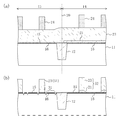
しかしながら、前述のハイブリッドメタルゲート電極の形成方法においては、フォトリソグラフィ及びドライエッチングを用いてゲート電極材料膜をパターニングしてゲート電極を形成する際に、pMIS構造とnMOS構造との違いであるpMIS構造用のメタル材料を所定の領域以外ではエッチングによって完全に除去する必要があると共に、当該エッチングを下地のゲート絶縁膜でストップさせる必要がある。この場合、pMIS構造とnMOS構造との違いであるメタル材料をエッチングして完全に除去するために必要なオーバーエッチングにより、膜厚が1〜3nm程度の薄膜であるゲート絶縁膜の突き抜けが発生し、下地の半導体基板(シリコン基板)がむき出しとなってシリコン基板が掘れ下がり、それによってシリコン基板削れ(例えば図24(b)に示す基板削れ31)が発生するという問題がある。特に、素子分離と活性領域との境界に段差が生じている場合には、当該段差部においてメタル材料膜が厚くなり、このメタル材料膜を完全に除去するために、nMOS側のゲート絶縁膜に対するオーバーエッチング量が大きくなる結果、ゲート絶縁膜の突き抜け及びそれに伴う基板削れに起因する問題、例えばトランジスタ特性劣化やパーティクル増加等がより顕在化する。図25は、前述の従来のハイブリッドメタルゲート電極構造を用いたCMOSFETの形成方法における図23(a)に示す工程で、素子分離12と活性領域との境界に段差が生じ、当該段差部においてメタル材料膜であるゲート電極材料膜21が厚膜化(厚膜化した厚さを両矢印50で示している)した様子を示している。
However, in the hybrid metal gate electrode formation method described above, the pMIS structure is the difference between the pMIS structure and the nMOS structure when the gate electrode material film is patterned by photolithography and dry etching to form the gate electrode. It is necessary to completely remove the metal material for etching outside the predetermined region by etching, and it is necessary to stop the etching with the underlying gate insulating film. In this case, the over-etching required to completely remove the metal material, which is the difference between the pMIS structure and the nMOS structure, causes a penetration of the gate insulating film, which is a thin film having a thickness of about 1 to 3 nm. There is a problem that the underlying semiconductor substrate (silicon substrate) is exposed and the silicon substrate is dug down, thereby causing silicon substrate scraping (for example,
前記に鑑み、本願発明は、ハイブリッドメタルゲート電極においてゲート絶縁膜の突き抜けが発生しない半導体装置及びその製造方法を提供することを目的とする。 In view of the above, an object of the present invention is to provide a semiconductor device in which a gate insulating film does not penetrate in a hybrid metal gate electrode and a method for manufacturing the same.
前記の目的を達成するために、本願第1発明に係る半導体装置は、半導体基板上に形成されたnチャネル型電界効果トランジスタ及びpチャネル型電界効果トランジスタを有する半導体装置であって、前記nチャネル型電界効果トランジスタ及び前記pチャネル型電界効果トランジスタのうちの一方のトランジスタのゲート電極は、ゲート絶縁膜と接する金属含有層と、前記金属含有層の上に形成された第1のシリコン含有層とを含み、前記nチャネル型電界効果トランジスタ及び前記pチャネル型電界効果トランジスタのうちの他方のトランジスタのゲート電極は、ゲート絶縁膜と接する第2のシリコン含有層と、前記第2のシリコン含有層の上に形成された第3のシリコン含有層とを含み、前記第1のシリコン含有層と前記第3のシリコン含有層とは同一のシリコン含有材料膜から形成されている。 In order to achieve the above object, a semiconductor device according to the first invention of the present application is a semiconductor device having an n-channel field effect transistor and a p-channel field effect transistor formed on a semiconductor substrate, wherein the n-channel field effect transistor is provided. The gate electrode of one of the p-type field effect transistor and the p-channel field effect transistor has a metal-containing layer in contact with the gate insulating film, a first silicon-containing layer formed on the metal-containing layer, A gate electrode of the other of the n-channel field effect transistor and the p-channel field effect transistor includes: a second silicon-containing layer in contact with a gate insulating film; and the second silicon-containing layer. A third silicon-containing layer formed thereon, the first silicon-containing layer and the third silicon It is formed of the same silicon-containing material film and the containing layer.
また、本願第1発明の半導体装置を製造するための本願第2発明に係る半導体装置の製造方法は、第1のトランジスタ領域と第2のトランジスタ領域とを有する半導体基板上にゲート絶縁膜を形成する工程(a)と、前記ゲート絶縁膜の上に第1のシリコン含有材料膜を形成する工程(b)と、前記第1のトランジスタ領域上に位置する部分の前記第1のシリコン含有材料膜を除去する工程(c)と、前記工程(c)の後に、前記第1のトランジスタ領域上に位置する部分の前記ゲート絶縁膜の上、及び前記第2のトランジスタ領域上に位置する部分の前記第1のシリコン含有材料膜の上に金属含有材料膜を形成する工程(d)と、前記第2のトランジスタ領域上に位置する部分の前記金属含有材料膜を除去する工程(e)と、前記工程(e)の後に、前記第1のトランジスタ領域上に位置する部分の前記金属含有材料膜の上、及び前記第2のトランジスタ領域上に位置する部分の前記第1のシリコン含有材料膜の上に第2のシリコン含有材料膜を形成する工程(f)と、前記第1のトランジスタ領域上において前記金属含有材料膜及び前記第2のシリコン含有材料膜をパターニングすることによって第1のゲート電極を形成すると共に、前記第2のトランジスタ領域上において前記第1のシリコン含有材料膜及び前記第2のシリコン含有材料膜をパターニングすることによって第2のゲート電極を形成する工程(g)とを備えている。 In addition, a method of manufacturing a semiconductor device according to the second invention of the present application for manufacturing a semiconductor device of the first invention of the present application forms a gate insulating film on a semiconductor substrate having a first transistor region and a second transistor region. A step (a), a step (b) of forming a first silicon-containing material film on the gate insulating film, and a portion of the first silicon-containing material film located on the first transistor region (C), and after the step (c), the portion of the gate insulating film located on the first transistor region and the portion of the second transistor region located on the second transistor region A step (d) of forming a metal-containing material film on the first silicon-containing material film; a step (e) of removing the portion of the metal-containing material film located on the second transistor region; Process (e After the second over the portion of the metal-containing material film located on the first transistor region and over the portion of the first silicon-containing material film located over the second transistor region. Forming a first gate electrode by patterning the metal-containing material film and the second silicon-containing material film in the step (f) of forming a silicon-containing material film, and on the first transistor region; And (g) forming a second gate electrode by patterning the first silicon-containing material film and the second silicon-containing material film on the second transistor region.
また、前記の目的を達成するために、本願第3発明に係る半導体装置は、半導体基板上に形成されたnチャネル型電界効果トランジスタ及びpチャネル型電界効果トランジスタを有する半導体装置であって、前記nチャネル型電界効果トランジスタ及び前記pチャネル型電界効果トランジスタのうちの一方のトランジスタのゲート電極は、ゲート絶縁膜と接する金属含有層と、前記金属含有層の上に形成された第1の導電性酸化物層と、前記第1の導電性酸化物層の上に形成された第1のシリコン含有層とを含み、前記nチャネル型電界効果トランジスタ及び前記pチャネル型電界効果トランジスタのうちの他方のトランジスタのゲート電極は、ゲート絶縁膜と接する第2のシリコン含有層と、前記第2のシリコン含有層の上に形成された第2の導電性酸化物層と、前記第2の導電性酸化物層の上に形成された第3のシリコン含有層とを含み、前記第1のシリコン含有層と前記第3のシリコン含有層とは同一のシリコン含有材料膜から形成されている。 In order to achieve the above object, a semiconductor device according to the third invention of the present application is a semiconductor device having an n-channel field effect transistor and a p-channel field effect transistor formed on a semiconductor substrate, The gate electrode of one of the n-channel field effect transistor and the p-channel field effect transistor has a metal-containing layer in contact with a gate insulating film, and a first conductivity formed on the metal-containing layer. An oxide layer and a first silicon-containing layer formed on the first conductive oxide layer, the other of the n-channel field effect transistor and the p-channel field effect transistor A gate electrode of the transistor includes a second silicon-containing layer in contact with the gate insulating film, and a second silicon-containing layer formed on the second silicon-containing layer. And a third silicon-containing layer formed on the second conductive oxide layer, wherein the first silicon-containing layer and the third silicon-containing layer are The same silicon-containing material film is formed.
また、本願第3発明の半導体装置を製造するための本願第4発明に係る半導体装置の製造方法は、第1のトランジスタ領域と第2のトランジスタ領域とを有する半導体基板上にゲート絶縁膜を形成する工程(a)と、前記ゲート絶縁膜の上に第1のシリコン含有材料膜及び第1の導電性酸化物膜を順次形成する工程(b)と、前記第1のトランジスタ領域上に位置する部分の前記第1の導電性酸化物膜及び前記第1のシリコン含有材料膜を除去する工程(c)と、前記工程(c)の後に、前記第1のトランジスタ領域上に位置する部分の前記ゲート絶縁膜の上、及び前記第2のトランジスタ領域上に位置する部分の前記第1の導電性酸化物膜の上に金属含有材料膜及び第2の導電性酸化物膜を順次形成する工程(d)と、前記第2のトランジスタ領域上に位置する部分の前記第2の導電性酸化物膜及び前記金属含有材料膜を除去する工程(e)と、前記工程(e)の後に、前記第1のトランジスタ領域上に位置する部分の前記第2の導電性酸化物膜の上、及び前記第2のトランジスタ領域上に位置する部分の前記第1の導電性酸化物膜の上に第2のシリコン含有材料膜を形成する工程(f)と、前記第1のトランジスタ領域上において前記金属含有材料膜、前記第2の導電性酸化物膜及び前記第2のシリコン含有材料膜をパターニングすることによって第1のゲート電極を形成すると共に、前記第2のトランジスタ領域上において前記第1のシリコン含有材料膜、前記第1の導電性酸化物膜及び前記第2のシリコン含有材料膜をパターニングすることによって第2のゲート電極を形成する工程(g)とを備えている。 A method of manufacturing a semiconductor device according to the fourth invention of the present application for manufacturing a semiconductor device of the third invention of the present application forms a gate insulating film on a semiconductor substrate having a first transistor region and a second transistor region. A step (a), a step (b) of sequentially forming a first silicon-containing material film and a first conductive oxide film on the gate insulating film, and a position on the first transistor region. Removing the portion of the first conductive oxide film and the first silicon-containing material film, and after the step (c), the portion of the portion located on the first transistor region; A step of sequentially forming a metal-containing material film and a second conductive oxide film on the gate insulating film and on the first conductive oxide film in a portion located on the second transistor region ( d) and the second transition A step (e) of removing the second conductive oxide film and the metal-containing material film in a portion located on the first transistor region, and a step located on the first transistor region after the step (e). Forming a second silicon-containing material film on a portion of the second conductive oxide film and on a portion of the first conductive oxide film located on the second transistor region; (F) and forming the first gate electrode by patterning the metal-containing material film, the second conductive oxide film, and the second silicon-containing material film on the first transistor region. And forming a second gate electrode by patterning the first silicon-containing material film, the first conductive oxide film, and the second silicon-containing material film on the second transistor region. And a step (g) to.
本願第1〜第4発明によると、ゲート絶縁膜と接する金属含有材料膜(金属含有層)がゲート電極の一部として形成されない第2のトランジスタ領域(他方のトランジスタ領域)上には、金属含有材料膜のエッチング時にオーバーエッチング吸収層として機能する第1のシリコン含有材料膜(第2のシリコン含有層)を予め形成している。このため、金属含有材料膜のエッチング時にゲート絶縁膜に対するオーバーエッチング量が各トランジスタ領域で実質的に同等となるように第1のシリコン含有材料膜の膜厚等を設定することにより、各トランジスタ領域間でのゲート絶縁膜に対するオーバーエッチング量の不均一性を低減できる。従って、ゲート絶縁膜の突き抜け及びそれに伴う基板削れ等を防止できるため、トランジスタ特性劣化やパーティクル増加等に起因する歩留まり低下の危険を回避でき、それによって高性能な半導体装置を安価で提供することができる。 According to the first to fourth inventions of the present application, the metal-containing material film (metal-containing layer) that is in contact with the gate insulating film is not formed as a part of the gate electrode on the second transistor region (the other transistor region). A first silicon-containing material film (second silicon-containing layer) that functions as an overetching absorption layer when the material film is etched is formed in advance. Therefore, by setting the thickness of the first silicon-containing material film and the like so that the amount of overetching with respect to the gate insulating film is substantially equal in each transistor region when the metal-containing material film is etched, It is possible to reduce the non-uniformity of the overetching amount for the gate insulating film. Therefore, it is possible to prevent the gate insulating film from penetrating and the accompanying substrate scraping, etc., so that it is possible to avoid the risk of yield reduction due to transistor characteristic deterioration, particle increase, etc., thereby providing a high-performance semiconductor device at low cost. it can.
また、本願第1〜第4発明によると、ゲート電極加工時のエッチングにおけるオーバーエッチング量が各トランジスタ領域において実質的に同等となるため、オーバーエッチングに伴うゲート寸法変化を各トランジスタ領域で揃えることができる。このため、各トランジスタ、具体的にはnチャネル型電界効果トランジスタ及びpチャネル型電界効果トランジスタのそれぞれにおけるゲート寸法のばらつきを低減することが可能となり、トランジスタ特性がより安定した半導体装置を提供することができる。 In addition, according to the first to fourth inventions of the present application, the amount of over-etching during gate electrode processing is substantially the same in each transistor region, so that the gate dimension change due to over-etching can be made uniform in each transistor region. it can. Therefore, it is possible to reduce variations in gate dimensions of each transistor, specifically, an n-channel field effect transistor and a p-channel field effect transistor, and provide a semiconductor device with more stable transistor characteristics. Can do.
尚、本願第1発明の半導体装置において、前記第2のシリコン含有層及び第3のシリコン含有層の全体がシリサイド層であってもよい。 In the semiconductor device according to the first aspect of the present invention, the second silicon-containing layer and the third silicon-containing layer may be entirely silicide layers.
また、本願第2発明の半導体装置の製造方法において、前記工程(c)は、前記第2のトランジスタ領域上に位置する部分の前記第1のシリコン含有材料膜を覆うエッチングカバー膜を用いて、前記第1のトランジスタ領域上に位置する部分の前記第1のシリコン含有材料膜を除去する工程を含み、前記工程(f)の前に、前記エッチングカバー膜を除去する工程をさらに備えていてもよい。この場合、前記工程(e)は、前記第1のトランジスタ領域上に位置する部分の前記金属含有材料膜を覆う他のエッチングカバー膜を用いて、前記第2のトランジスタ領域上に位置する部分の前記金属含有材料膜を除去する工程を含み、前記工程(f)の前に、前記他のエッチングカバー膜を除去する工程をさらに備えていてもよい。 In the method for manufacturing a semiconductor device according to the second invention of the present application, the step (c) uses an etching cover film that covers the first silicon-containing material film in a portion located on the second transistor region. A step of removing the portion of the first silicon-containing material film located on the first transistor region, and further comprising a step of removing the etching cover film before the step (f). Good. In this case, in the step (e), another etching cover film that covers the metal-containing material film in the portion located on the first transistor region is used to form the portion located on the second transistor region. It may include a step of removing the metal-containing material film, and further comprising a step of removing the other etching cover film before the step (f).
また、本願第3発明の半導体装置において、前記第1の導電性酸化物層及び前記第2の導電性酸化物層は、Ir及びRuのうちの少なくとも1つを含む酸化物から構成されていてもよい。 In the semiconductor device of the third invention of the present application, the first conductive oxide layer and the second conductive oxide layer are made of an oxide containing at least one of Ir and Ru. Also good.
前記の目的を達成するために、本願第5発明に係る半導体装置は、半導体基板上に形成されたnチャネル型電界効果トランジスタ及びpチャネル型電界効果トランジスタを有する半導体装置であって、前記nチャネル型電界効果トランジスタ及び前記pチャネル型電界効果トランジスタのうちの一方のトランジスタのゲート電極は、ゲート絶縁膜と接する金属含有層と、前記金属含有層の上に形成された第1のシリコン含有層とを含み、前記nチャネル型電界効果トランジスタ及び前記pチャネル型電界効果トランジスタのうちの他方のトランジスタのゲート電極は、ゲート絶縁膜と接する第2のシリコン含有層と、前記第2のシリコン含有層の上に形成された導電性酸化物層と、前記導電性酸化物層の上に形成された他の金属含有層と、前記他の金属含有層の上に形成された第3のシリコン含有層とを含み、前記金属含有層と前記他の金属含有層とは同一の金属含有膜から形成されており、前記第1のシリコン含有層と前記第3のシリコン含有層とは同一のシリコン含有材料膜から形成されている。 In order to achieve the above object, a semiconductor device according to a fifth aspect of the present invention is a semiconductor device having an n-channel field effect transistor and a p-channel field effect transistor formed on a semiconductor substrate, wherein the n-channel field effect transistor is provided. The gate electrode of one of the p-type field effect transistor and the p-channel field effect transistor includes a metal-containing layer in contact with a gate insulating film, a first silicon-containing layer formed on the metal-containing layer, A gate electrode of the other of the n-channel field effect transistor and the p-channel field effect transistor includes: a second silicon-containing layer in contact with a gate insulating film; and the second silicon-containing layer. A conductive oxide layer formed thereon; another metal-containing layer formed on said conductive oxide layer; and A third silicon-containing layer formed on another metal-containing layer, wherein the metal-containing layer and the other metal-containing layer are formed of the same metal-containing film, and the first silicon The containing layer and the third silicon-containing layer are formed from the same silicon-containing material film.
また、本願第5発明の半導体装置を製造するための本願第6発明に係る半導体装置の製造方法は、第1のトランジスタ領域と第2のトランジスタ領域とを有する半導体基板上にゲート絶縁膜を形成する工程(a)と、前記ゲート絶縁膜の上に第1のシリコン含有材料膜及び導電性酸化物膜を順次形成する工程(b)と、前記第1のトランジスタ領域上に位置する部分の前記導電性酸化物膜及び前記第1のシリコン含有材料膜を除去する工程(c)と、前記工程(c)の後に、前記第1のトランジスタ領域上に位置する部分の前記ゲート絶縁膜の上、及び前記第2のトランジスタ領域上に位置する部分の前記導電性酸化物膜の上に金属含有材料膜及び第2のシリコン含有材料膜を順次形成する工程(d)と、前記第1のトランジスタ領域上において前記第2のシリコン含有材料膜及び前記金属含有材料膜をパターニングすることによって第1のゲート電極を形成すると共に、前記第2のトランジスタ領域上において前記第2のシリコン含有材料膜及び前記金属含有材料膜をゲート電極形状にパターニングする工程(e)と、前記工程(e)の後に、前記第1のトランジスタ領域及び前記第2のトランジスタ領域を覆う絶縁膜を形成する工程(f)と、前記第1のトランジスタ領域をレジストによって保護しながら、前記第2のトランジスタ領域上において前記絶縁膜及び前記導電性酸化物膜をエッチバックした後、前記レジストを除去し、その後、前記第1のトランジスタ領域を前記絶縁膜によって保護しながら、前記第2のトランジスタ領域上において前記第1のシリコン含有材料膜をゲート電極形状にパターニングすることによって第2のゲート電極を形成する工程(g)と、前記工程(g)の後に、前記第1のトランジスタ領域上に残存する前記絶縁膜を除去する工程(h)とを備えている。 A method for manufacturing a semiconductor device according to a sixth invention for manufacturing a semiconductor device according to a fifth invention of the present application includes forming a gate insulating film on a semiconductor substrate having a first transistor region and a second transistor region. A step (a), a step (b) of sequentially forming a first silicon-containing material film and a conductive oxide film on the gate insulating film, and a portion of the portion located on the first transistor region. A step (c) of removing a conductive oxide film and the first silicon-containing material film, and after the step (c), on a portion of the gate insulating film located on the first transistor region; And (d) sequentially forming a metal-containing material film and a second silicon-containing material film on a portion of the conductive oxide film located on the second transistor region, and the first transistor region On top Forming the first gate electrode by patterning the second silicon-containing material film and the metal-containing material film, and forming the second silicon-containing material film and the metal-containing material on the second transistor region. A step (e) of patterning a material film into a gate electrode shape; a step (f) of forming an insulating film covering the first transistor region and the second transistor region after the step (e); The insulating film and the conductive oxide film are etched back on the second transistor region while the first transistor region is protected by a resist, and then the resist is removed, and then the first transistor region The first silicon-containing material is formed on the second transistor region while protecting the substrate with the insulating film. Forming a second gate electrode by patterning the gate electrode into a gate electrode shape, and removing the insulating film remaining on the first transistor region after the step (g) (h) ).
また、前記の目的を達成するために、本願第7発明に係る半導体装置は、半導体基板上に形成されたnチャネル型電界効果トランジスタ及びpチャネル型電界効果トランジスタを有する半導体装置であって、前記nチャネル型電界効果トランジスタ及び前記pチャネル型電界効果トランジスタのうちの一方のトランジスタのゲート電極は、ゲート絶縁膜と接する金属含有層と、前記金属含有層の上に形成された導電性酸化物層と、前記導電性酸化物層の上に形成されたシリコン含有層とを含み、前記nチャネル型電界効果トランジスタ及び前記pチャネル型電界効果トランジスタのうちの他方のトランジスタのゲート電極は、ゲート絶縁膜と接する他のシリコン含有層を含み、前記シリコン含有層と前記他のシリコン含有層とは同一のシリコン含有材料膜から形成されている。 In order to achieve the above object, a semiconductor device according to a seventh aspect of the present invention is a semiconductor device having an n-channel field effect transistor and a p-channel field effect transistor formed on a semiconductor substrate, The gate electrode of one of the n-channel field effect transistor and the p-channel field effect transistor has a metal-containing layer in contact with a gate insulating film, and a conductive oxide layer formed on the metal-containing layer And a silicon-containing layer formed on the conductive oxide layer, and the gate electrode of the other of the n-channel field effect transistor and the p-channel field effect transistor is a gate insulating film The silicon-containing layer and the other silicon-containing layer are the same silicon. It formed from containing material film.
また、本願第7発明の半導体装置を製造するための本願第8発明に係る半導体装置の製造方法は、第1のトランジスタ領域と第2のトランジスタ領域とを有する半導体基板上にゲート絶縁膜を形成する工程(a)と、前記ゲート絶縁膜の上に金属含有材料膜及び導電性酸化物膜を形成する工程(b)と、前記第2のトランジスタ領域上に位置する部分の前記導電性酸化物膜及び前記金属含有材料膜を除去する工程(c)と、前記工程(c)の後に、前記第1のトランジスタ領域上に位置する部分の前記導電性酸化物膜の上、及び前記第2のトランジスタ領域上に位置する部分の前記ゲート絶縁膜の上にシリコン含有材料膜を形成する工程(d)と、前記第1のトランジスタ領域上において前記シリコン含有材料膜をゲート電極形状にパターニングすると共に、前記第2のトランジスタ領域上において前記シリコン含有材料膜をパターニングすることによって第2のゲート電極を形成する工程(e)と、前記工程(e)の後に、前記第1のトランジスタ領域及び前記第2のトランジスタ領域を覆う絶縁膜を形成する工程(f)と、前記第2のトランジスタ領域をレジストによって保護しながら、前記第1のトランジスタ領域上において前記絶縁膜及び前記導電性酸化物膜をエッチバックした後、前記レジストを除去し、その後、前記第2のトランジスタ領域を前記絶縁膜によって保護しながら、前記第1のトランジスタ領域上において前記金属含有材料膜をゲート電極形状にパターニングすることによって第1のゲート電極を形成する工程(g)と、前記工程(g)の後に、前記第2のトランジスタ領域上に残存する前記絶縁膜を除去する工程(h)とを備えている。 A method for manufacturing a semiconductor device according to the eighth invention of the present application for manufacturing the semiconductor device of the seventh invention of the present application includes forming a gate insulating film on a semiconductor substrate having a first transistor region and a second transistor region. Step (a), forming (b) a metal-containing material film and a conductive oxide film on the gate insulating film, and a portion of the conductive oxide located on the second transistor region (C) removing the film and the metal-containing material film, and after the step (c), on the conductive oxide film in a portion located on the first transistor region, and the second A step (d) of forming a silicon-containing material film on a portion of the gate insulating film located on the transistor region; and patterning the silicon-containing material film into a gate electrode shape on the first transistor region. And (e) forming a second gate electrode by patterning the silicon-containing material film on the second transistor region, and after the step (e), the first transistor region And (f) forming an insulating film covering the second transistor region, and protecting the second transistor region with a resist while the insulating film and the conductive oxide are formed on the first transistor region. After etching back the film, the resist is removed, and then the metal-containing material film is patterned into a gate electrode shape on the first transistor region while protecting the second transistor region with the insulating film. After the step (g) for forming the first gate electrode and the step (g), the second gate electrode is formed. And a step (h) of removing the insulating film remaining on the transistor region.
本願第5〜第8発明によると、ゲート電極加工時のエッチングにおいてオーバーエッチングの実施前に、オーバーエッチング量が大きくなるトランジスタ領域を覆うように、エッチングストッパー膜として機能する絶縁膜を予め形成している。このため、ゲート絶縁膜の突き抜け及びそれに伴う基板削れ等を防止できるため、トランジスタ特性劣化やパーティクル増加等に起因する歩留まり低下の危険を回避でき、それによって高性能な半導体装置を安価で提供することができる。 According to the fifth to eighth inventions of the present application, an insulating film functioning as an etching stopper film is formed in advance so as to cover a transistor region in which the amount of over-etching becomes large before performing over-etching in etching during gate electrode processing. Yes. For this reason, it is possible to prevent the gate insulating film from penetrating and the accompanying substrate scraping, etc., thereby avoiding the risk of yield reduction due to transistor characteristics deterioration, particle increase, etc., thereby providing a high-performance semiconductor device at low cost. Can do.
また、本願第5〜第8発明によると、ゲート電極加工時のエッチングにおけるオーバーエッチング量が各トランジスタ領域において過剰とならないため、オーバーエッチングに伴うゲート寸法変化を各トランジスタ領域で揃えることができる。このため、各トランジスタ、具体的にはnチャネル型電界効果トランジスタ及びpチャネル型電界効果トランジスタのそれぞれにおけるゲート寸法のばらつきを低減することが可能となり、トランジスタ特性がより安定した半導体装置を提供することができる。 In addition, according to the fifth to eighth inventions of the present application, since the overetching amount in the etching at the time of processing the gate electrode does not become excessive in each transistor region, the gate dimension change accompanying the overetching can be made uniform in each transistor region. Therefore, it is possible to reduce variations in gate dimensions of each transistor, specifically, an n-channel field effect transistor and a p-channel field effect transistor, and provide a semiconductor device with more stable transistor characteristics. Can do.
尚、本願第5発明の半導体装置において、前記金属含有層と前記第1のシリコン含有層との積層構造の側面には第1のオフセットスペーサが形成されており、前記第2のシリコン含有層と前記導電性酸化物層との積層構造の側面には第2のオフセットスペーサが形成されており、前記第1のオフセットスペーサは第1のオフセット膜及びその外側に形成された第2のオフセット膜の積層膜から構成されており、前記第2のオフセットスペーサは前記第2のオフセット膜の単層膜から構成されていてもよい。この場合、前記第2のオフセットスペーサは、前記他の金属含有層と前記第3のシリコン含有層との積層構造の側面においては前記第1のオフセット膜及び前記第2のオフセット膜の積層膜から構成されていてもよい。すなわち、前記第2のシリコン含有層と前記導電性酸化物層との積層構造の幅は、前記他の金属含有層と前記第3のシリコン含有層との積層構造の幅よりも大きく、前記第2のシリコン含有層と前記導電性酸化物層との積層構造の側面における前記第2のオフセットスペーサの幅は、前記他の金属含有層と前記第3のシリコン含有層との積層構造の側面における前記第2のオフセットスペーサの幅よりも小さくてもよい。 In the semiconductor device of the fifth invention of the present application, a first offset spacer is formed on a side surface of the laminated structure of the metal-containing layer and the first silicon-containing layer, and the second silicon-containing layer and A second offset spacer is formed on a side surface of the stacked structure with the conductive oxide layer, and the first offset spacer includes a first offset film and a second offset film formed outside the first offset film. The second offset spacer may be composed of a single layer film of the second offset film. In this case, the second offset spacer is formed from the laminated film of the first offset film and the second offset film on the side surface of the laminated structure of the other metal-containing layer and the third silicon-containing layer. It may be configured. That is, the width of the stacked structure of the second silicon-containing layer and the conductive oxide layer is larger than the width of the stacked structure of the other metal-containing layer and the third silicon-containing layer. The width of the second offset spacer on the side surface of the stacked structure of the silicon-containing layer of 2 and the conductive oxide layer is the width of the side surface of the stacked structure of the other metal-containing layer and the third silicon-containing layer. The width may be smaller than the width of the second offset spacer.
また、本願第1、第3、第5発明の半導体装置において、前記第1のシリコン含有層及び前記第3のシリコン含有層のそれぞれの少なくとも上部は、Ni、Co、Ti、W及びPtのうちの少なくとも1つを含むシリサイド層であってもよい。 In the semiconductor device of the first, third, and fifth inventions of the present application, at least an upper portion of each of the first silicon-containing layer and the third silicon-containing layer is made of Ni, Co, Ti, W, and Pt. A silicide layer including at least one of the above may be used.
また、本願第1、第3、第5発明の半導体装置において、前記第2のシリコン含有層は、ポリシリコン、アモルファスシリコン又はシリコンゲルマニウムに、P(燐)、As(砒素)、B(ホウ素)、In(インジウム)、N(窒素)、C(炭素)及びF(フッ素)のうちから選ばれた少なくとも1つの不純物をドーピングした材料から構成されていてもよい。 In the first, third, and fifth inventions of the present application, the second silicon-containing layer may be polysilicon, amorphous silicon, or silicon germanium, P (phosphorus), As (arsenic), B (boron). , In (indium), N (nitrogen), C (carbon), and F (fluorine), and may be made of a material doped with at least one impurity.
また、本願第6発明の半導体装置の製造方法において、前記工程(f)は、前記第2のトランジスタ領域上においてパターニングされた前記第2のシリコン含有材料膜及び前記金属含有材料膜のそれぞれの側面を覆うように前記絶縁膜を形成する工程を含み、前記工程(h)は、前記半導体基板上の全面に他の絶縁膜を形成した後、当該他の絶縁膜及び前記絶縁膜に対してエッチバックを行って、前記第1のゲート電極の側面に前記絶縁膜及び前記他の絶縁膜の積層膜からなる第1のオフセットスペーサを形成すると共に、前記第2のゲート電極のうちの前記第2のシリコン含有材料膜及び前記金属含有材料膜のそれぞれの側面を覆う前記絶縁膜と当該絶縁膜並びに前記第2のゲート電極のうちの前記導電性酸化物膜及び前記第1のシリコン含有材料膜のそれぞれの側面を覆う前記他の絶縁膜とからなる第2のオフセットスペーサを形成する形成する工程を含んでいてもよい。 Further, in the method of manufacturing a semiconductor device according to the sixth aspect of the present invention, the step (f) includes side surfaces of the second silicon-containing material film and the metal-containing material film patterned on the second transistor region. The step (h) includes forming another insulating film on the entire surface of the semiconductor substrate, and then etching the other insulating film and the insulating film. Backing is performed to form a first offset spacer comprising a laminated film of the insulating film and the other insulating film on the side surface of the first gate electrode, and the second of the second gate electrodes. The silicon-containing material film and the insulating film covering the side surfaces of the metal-containing material film, the insulating film, and the conductive oxide film and the first silicon of the second gate electrode Each side may comprise the step of forming forms a second offset spacer consisting of said other insulating film covering the perforated material film.
また、本願第7発明の半導体装置において、前記他のシリコン含有層の全体がシリサイド層であってもよい。 In the semiconductor device of the seventh invention of the present application, the entire other silicon-containing layer may be a silicide layer.
また、本願第7発明の半導体装置において、前記シリコン含有層及び前記他のシリコン含有層のそれぞれの少なくとも上部は、Ni、Co、Ti、W及びPtのうちの少なくとも1つを含むシリサイド層であってもよい。 In the semiconductor device of the seventh invention of the present application, at least the upper portions of the silicon-containing layer and the other silicon-containing layer are silicide layers containing at least one of Ni, Co, Ti, W, and Pt. May be.
また、本願第7発明の半導体装置において、前記金属含有層と前記導電性酸化物層との積層構造の側面には第1のオフセットスペーサが形成されており、前記他のシリコン含有層の側面には第2のオフセットスペーサが形成されており、前記第2のオフセットスペーサは第1のオフセット膜及びその外側に形成された第2のオフセット膜の積層膜から構成されており、前記第1のオフセットスペーサは前記第2のオフセット膜の単層膜から構成されていてもよい。この場合、前記第1のオフセットスペーサは、前記シリコン含有層の側面においては前記第1のオフセット膜及び前記第2のオフセット膜の積層膜から構成されていてもよい。すなわち、前記金属含有層と前記導電性酸化物層との積層構造の幅は、前記シリコン含有層の幅よりも大きく、前記金属含有層と前記導電性酸化物層との積層構造の側面における前記第1のオフセットスペーサの幅は、前記シリコン含有層の側面における前記第2のオフセットスペーサの幅よりも小さくてもよい。 In the semiconductor device of the seventh invention of the present application, a first offset spacer is formed on a side surface of the stacked structure of the metal-containing layer and the conductive oxide layer, and on the side surface of the other silicon-containing layer. Has a second offset spacer, and the second offset spacer includes a first offset film and a laminated film of a second offset film formed outside the first offset film, and the first offset spacer is formed. The spacer may be composed of a single layer film of the second offset film. In this case, the first offset spacer may be formed of a laminated film of the first offset film and the second offset film on the side surface of the silicon-containing layer. That is, the width of the stacked structure of the metal-containing layer and the conductive oxide layer is larger than the width of the silicon-containing layer, and the side surface of the stacked structure of the metal-containing layer and the conductive oxide layer is The width of the first offset spacer may be smaller than the width of the second offset spacer on the side surface of the silicon-containing layer.
また、本願第5、第7発明の半導体装置において、第1及び第2のオフセットスペーサが形成されている場合、前記第1のオフセット膜及び前記第2のオフセット膜はそれぞれ、シリコン酸化膜、シリコン窒化膜、シリコン炭化膜、シリコン酸化窒化膜又はシリコン酸化炭化膜であってもよい。 In the semiconductor devices of the fifth and seventh inventions of the present application, when the first and second offset spacers are formed, the first offset film and the second offset film are a silicon oxide film and a silicon oxide film, respectively. A nitride film, a silicon carbide film, a silicon oxynitride film, or a silicon oxycarbide film may be used.
また、本願第5、第7発明の半導体装置において、前記導電性酸化物層は、Ir及びRuのうちの少なくとも1つを含む酸化物から構成されていてもよい。 In the semiconductor devices of the fifth and seventh inventions of the present application, the conductive oxide layer may be made of an oxide containing at least one of Ir and Ru.
また、本願第1、第3、第5、第7発明の半導体装置において、前記金属含有層は、Ni、Pd、Pt、Co、Rh、Ru、Cu、Ag及びAuからなる金属群から選ばれた少なくとも1つの金属よりなる金属膜、又は前記金属群から選ばれた少なくとも1つの金属の珪化物若しくは炭化物からなる膜であってもよい。 In the first, third, fifth, and seventh inventions of the present application, the metal-containing layer is selected from a metal group consisting of Ni, Pd, Pt, Co, Rh, Ru, Cu, Ag, and Au. Alternatively, it may be a metal film made of at least one metal, or a film made of silicide or carbide of at least one metal selected from the metal group.
また、本願第1、第3、第5、第7発明の半導体装置において、前記金属含有層は、Ti、Zr、Hf、V、Nb、Ta、Cr、Mo及びWからなる金属群から選ばれた少なくとも1つの金属よりなる金属膜、又は前記金属群から選ばれた少なくとも1つの金属の窒化物、珪化物若しくは炭化物からなる膜であってもよい。 In the first, third, fifth, and seventh inventions of the present application, the metal-containing layer is selected from a metal group consisting of Ti, Zr, Hf, V, Nb, Ta, Cr, Mo, and W. Alternatively, it may be a metal film made of at least one metal, or a film made of nitride, silicide or carbide of at least one metal selected from the metal group.
また、本願第1、第3、第5、第7発明の半導体装置において、前記ゲート絶縁膜は、SiO2 膜、HfO2 膜、HfAlx Oy 膜、HfSix Oy 膜若しくはこれらの膜に窒素を添加した膜からなる絶縁膜群から選ばれた1つの絶縁膜からなる単層膜、又は前記絶縁膜群から選ばれた少なくとも1つの絶縁膜を含む積層絶縁膜であってもよい。 In the semiconductor device of the first, third, fifth, and seventh inventions of the present application, the gate insulating film may be an SiO 2 film, an HfO 2 film, an HfAl x O y film, an HfSi x O y film, or a film thereof. It may be a single-layer film made of one insulating film selected from an insulating film group made of a film to which nitrogen is added, or a laminated insulating film including at least one insulating film selected from the insulating film group.
また、本願第8発明の半導体装置の製造方法において、前記工程(f)は、前記第1のトランジスタ領域上においてパターニングされた前記シリコン含有材料膜の側面を覆うように前記絶縁膜を形成する工程を含み、前記工程(h)は、前記半導体基板上の全面に他の絶縁膜を形成した後、当該他の絶縁膜及び前記絶縁膜に対してエッチバックを行って、前記第1のゲート電極のうちの前記シリコン含有材料膜の側面を覆う前記絶縁膜と当該絶縁膜並びに前記第1のゲート電極のうちの前記導電性酸化物膜及び前記金属含有材料膜のそれぞれの側面を覆う前記他の絶縁膜とからなる第1のオフセットスペーサを形成すると共に、前記第2のゲート電極の側面に前記絶縁膜及び前記他の絶縁膜の積層膜からなる第2のオフセットスペーサを形成する形成する工程を含んでいてもよい。 Further, in the method of manufacturing a semiconductor device according to the eighth invention of the present application, the step (f) includes a step of forming the insulating film so as to cover a side surface of the silicon-containing material film patterned on the first transistor region. In the step (h), after forming another insulating film on the entire surface of the semiconductor substrate, the other gate insulating film and the insulating film are etched back to form the first gate electrode. The insulating film covering the side surface of the silicon-containing material film, the insulating film, and the other covering the respective side surfaces of the conductive oxide film and the metal-containing material film of the first gate electrode. A first offset spacer made of an insulating film is formed, and a second offset spacer made of a laminated film of the insulating film and the other insulating film is formed on a side surface of the second gate electrode. It may include the step of forming that.
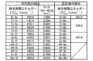
また、本願第1、第3発明の半導体装置において、前記金属含有層の厚さ及び前記第2のシリコン含有層の厚さは、前記金属含有層における金属M1と当該金属M1と同一又は異なる元素M2との間の結合を切断するためのエネルギーである結合解離エネルギーD(M1−M2)と、前記第2のシリコン含有層におけるシリコン結合を切断するためのエネルギーである結合解離エネルギーD(Si−Si)とに基づいて決定されていてもよい。この場合、前記結合解離エネルギーD(M1−M2)が前記結合解離エネルギーD(Si−Si)よりも大きい場合には、前記第2のシリコン含有層の厚さが前記金属含有層の厚さよりも大きく設定されており、前記結合解離エネルギーD(M1−M2)が前記結合解離エネルギーD(Si−Si)よりも小さい場合には、前記第2のシリコン含有層の厚さが前記金属含有層の厚さよりも小さく設定されていてもよい。また、前記金属含有層はTi又はTaからなり、前記第2のシリコン含有層はポリシリコンからなり、前記第2のシリコン含有層の厚さは前記金属含有層の厚さよりも小さく設定されていてもよい。また、前記金属含有層はTiN、TiC、TiO、TaN、TaC又はTaOからなり、前記第2のシリコン含有層はポリシリコンからなり、前記第2のシリコン含有層の厚さは前記金属含有層の厚さよりも大きく設定されていてもよい。 In the semiconductor devices of the first and third inventions of the present application, the thickness of the metal-containing layer and the thickness of the second silicon-containing layer are the same or different from the metal M1 and the metal M1 in the metal-containing layer. Bond dissociation energy D (M1-M2), which is energy for breaking the bond with M2, and bond dissociation energy D (Si-, which is energy for breaking the silicon bond in the second silicon-containing layer) And Si). In this case, when the bond dissociation energy D (M1-M2) is larger than the bond dissociation energy D (Si-Si), the thickness of the second silicon-containing layer is larger than the thickness of the metal-containing layer. When the bond dissociation energy D (M1-M2) is smaller than the bond dissociation energy D (Si-Si), the second silicon-containing layer has a thickness of the metal-containing layer. It may be set smaller than the thickness. The metal-containing layer is made of Ti or Ta, the second silicon-containing layer is made of polysilicon, and the thickness of the second silicon-containing layer is set smaller than the thickness of the metal-containing layer. Also good. The metal-containing layer is made of TiN, TiC, TiO, TaN, TaC or TaO, the second silicon-containing layer is made of polysilicon, and the thickness of the second silicon-containing layer is the same as that of the metal-containing layer. It may be set larger than the thickness.
また、本願第2、第4発明の半導体装置の製造方法において、前記第1のシリコン含有材料膜の厚さは、前記金属含有材料膜の厚さ、及び前記工程(g)における前記第1のシリコン含有材料膜と前記金属含有材料膜とのエッチングレート比に応じて、前記第1のシリコン含有材料膜及び前記金属含有材料膜のそれぞれのエッチングが完了する時間が実質的に同じになるように設定されていてもよい。この場合、前記第1のシリコン含有材料膜の厚さは、
TIME1 = TH1/ER1 ・・・ (式1)
TIME2 = TH2/ER2 ・・・ (式2)
TIME2×1.2>TIME1>TIME2×0.8 ・・・ (式3)
に従って設定されていてもよい(但し、TIME1は前記第1のシリコン含有材料膜のエッチングが完了するのに要する時間であり、TIME2は前記金属含有材料膜のエッチングが完了するのに要する時間であり、TH1は前記第1のシリコン含有材料膜の厚さであり、TH2は前記金属含有材料膜の厚さであり、ER1は前記工程(g)における前記第1のシリコン含有材料膜のエッチングレートであり、ER2は前記工程(g)における前記金属含有材料膜のエッチングレートである)。
Moreover, in the manufacturing method of the semiconductor device according to the second and fourth inventions of the present application, the thickness of the first silicon-containing material film is the thickness of the metal-containing material film, and the first in the step (g). Depending on the etching rate ratio between the silicon-containing material film and the metal-containing material film, the time for completing the etching of the first silicon-containing material film and the metal-containing material film is substantially the same. It may be set. In this case, the thickness of the first silicon-containing material film is
TIME1 = TH1 / ER1 (Formula 1)
TIME2 = TH2 / ER2 (Formula 2)
TIME2 × 1.2>TIME1> TIME2 × 0.8 (Formula 3)
(Where TIME1 is the time required to complete the etching of the first silicon-containing material film, and TIME2 is the time required to complete the etching of the metal-containing material film) , TH1 is the thickness of the first silicon-containing material film, TH2 is the thickness of the metal-containing material film, and ER1 is the etching rate of the first silicon-containing material film in the step (g). Yes, ER2 is the etching rate of the metal-containing material film in the step (g)).
尚、本願第1〜第8発明において、各トランジスタ領域毎にゲート絶縁膜を作り分けても良い。 In the first to eighth inventions of the present application, a gate insulating film may be formed separately for each transistor region.
本願発明によると、ゲート絶縁膜の突き抜け及びそれに伴う基板削れ等を防止できるため、トランジスタ特性劣化やパーティクル増加等に起因する歩留まり低下の危険を回避でき、それによって高性能な半導体装置を安価で提供することができる。 According to the present invention, it is possible to prevent the gate insulating film from penetrating and the accompanying substrate scraping, etc., so that it is possible to avoid the risk of yield reduction due to transistor characteristic degradation or particle increase, thereby providing a high-performance semiconductor device at a low cost. can do.
また、本願発明によると、ゲート電極加工時のエッチングにおけるオーバーエッチング量が各トランジスタ領域において実質的に同等となるため、オーバーエッチングに伴うゲート寸法変化を各トランジスタ領域で揃えることができる。このため、各トランジスタ、具体的にはnチャネル型電界効果トランジスタ及びpチャネル型電界効果トランジスタのそれぞれにおけるゲート寸法のばらつきを低減することが可能となり、トランジスタ特性がより安定した半導体装置を提供することができる。 In addition, according to the present invention, the amount of overetching in the etching at the time of processing the gate electrode is substantially equal in each transistor region, so that the gate dimension change due to overetching can be made uniform in each transistor region. Therefore, it is possible to reduce variations in gate dimensions of each transistor, specifically, an n-channel field effect transistor and a p-channel field effect transistor, and provide a semiconductor device with more stable transistor characteristics. Can do.
(第1の実施形態)
以下、本発明の第1の実施形態に係る半導体装置及びその製造方法について、図面を参照しながら説明する。
(First embodiment)
Hereinafter, a semiconductor device and a manufacturing method thereof according to a first embodiment of the present invention will be described with reference to the drawings.
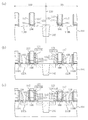
図1(a)〜(c)、図2(a)〜(c)及び図3(a)〜(c)は、本発明の第1の実施形態に係る半導体装置の製造方法の各工程を示す断面図である。尚、図1(a)〜(c)、図2(a)〜(c)及び図3(a)〜(c)において、np境界を符号110の破線で示している。
1A to 1C, FIGS. 2A to 2C, and FIGS. 3A to 3C illustrate respective steps of the method for manufacturing the semiconductor device according to the first embodiment of the present invention. It is sectional drawing shown. In FIGS. 1A to 1C, FIGS. 2A to 2C, and FIGS. 3A to 3C, the np boundary is indicated by a
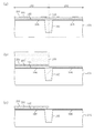
まず、図1(a)に示すように、半導体基板101に例えばSTI(Shallow Trench Isolation)からなる素子分離102を形成し、nチャネル領域103及びpチャネル領域104を区画した後、nチャネル領域103及びpチャネル領域104のそれぞれに対してウェル形成用イオン注入を実施する。次に、nチャネル領域103及びpチャネル領域104のそれぞれに対して、トランジスタの閾値を調整するためのイオン注入を実施する。次に、例えばロジックトランジスタ、SRAM(static random access memory )トランジスタ、及び入出力I/Oトランジスタ等の各トランジスタの機能に応じた膜厚及び膜質を持つゲート絶縁膜の作りこみを実施する。図1(a)は、nチャネル領域103及びpチャネル領域104のそれぞれの上に、例えばロジックトランジスタ用のゲート絶縁膜105を形成している場合を示している。具体的には、ゲート絶縁膜105は、半導体基板101の表面に形成された、シリコン酸化膜と比較して比誘電率の十分に高い高誘電率膜、例えばハフニウムシリコン酸化膜(HfSix Oy 膜)である。ここで、HfSix Oy 膜のEOT(シリコン酸化膜換算膜厚)は約2.0nmである。尚、ゲート絶縁膜105と半導体基板101との界面には、半導体基板101が酸化されてなる例えば厚さ1nm程度の極薄シリコン酸化膜が界面層106として形成されている。
First, as shown in FIG. 1A, an
次に、図1(a)に示すように、ゲート絶縁膜105の直上に、nチャネル領域103のトランジスタの閾値制御を行うための第1ゲート電極材料膜107として、例えばP(燐)をドーピングした厚さ5〜20nm程度のポリシリコン膜を堆積する。この第1ゲート電極材料膜107はオーバーエッチング吸収層として機能するものであり、後の工程で実施されるゲート電極加工時のドライエッチングにおいて、ゲート絶縁膜105へのオーバーエッチング量がnチャネル領域103及びpチャネル領域104で実質的に同等となるように、膜厚等が設定されている。
Next, as shown in FIG. 1A, for example, P (phosphorus) is doped immediately above the
次に、図1(b)に示すように、第1ゲート電極材料膜107の上に、pチャネル領域104を開口したレジストパターン109を形成した後、レジストパターン109をマスクとしてエッチングを行うことにより、pチャネル領域104上に位置する部分の第1ゲート電極材料膜107を除去する。ここで、第1ゲート電極材料膜107であるポリシリコン膜のエッチングには、例えば65℃に加熱した水酸化カリウム溶液(KOH/H2 O=0.3g/150cc)を用いる。これにより、ゲート絶縁膜105の膜減り等のダメージを防止しながらエッチングを行うことができる。或いは、例えば80℃に加熱した希釈APM(ammonia-hydrogen peroxide mixture )溶液(NH3 :H2 O2 :H2 O=3〜10:1:200〜1000)又は低ダメージのリモートプラズマを用いたケミカルドライエッチングによって第1ゲート電極材料膜107を除去することも可能である。さらには、例えばRIE(reative ion etching )によるドライエッチングによって第1ゲート電極材料膜107を途中まで除去した後に、前記の希釈APM溶液、水酸化カリウム溶液又は低ダメージのリモートプラズマを用いたケミカルドライエッチングを追加的に実施することによって第1ゲート電極材料膜107を除去することも可能である。この場合、np境界110におけるレジストパターン109の側面からnチャネル領域103上の第1ゲート電極材料膜107が後退する量を低減することができる。尚、第1ゲート電極材料膜107のエッチングの実施後、例えばSPM(sulfuric acid-hydrogen peroxide mixture )溶液又はシンナー溶液等を用いてレジストパターン109を除去する。
Next, as shown in FIG. 1B, a resist
次に、図1(c)に示すように、pチャネル領域104のトランジスタの閾値制御を行うための第2ゲート電極材料膜111として、例えば厚さ5〜20nm程度のTiN膜をnチャネル領域103上及びpチャネル領域104上のそれぞれの全面に堆積する。
Next, as shown in FIG. 1C, as the second gate
このとき、前述のオーバーエッチング吸収層となる第1ゲート電極材料膜107の膜厚は、pチャネル領域104のトランジスタの閾値制御を行うための第2ゲート電極材料111の膜厚、及びゲート加工での各ゲート電極材料膜のエッチングレート比に応じて、第1ゲート電極材料膜107及び第2ゲート電極材料膜111のそれぞれのエッチングが完了する時間が実質的に同じになるように予め設定されている。
At this time, the film thickness of the first gate
具体的には、オーバーエッチング吸収層となる第1ゲート電極材料膜107の膜厚の決定は下記(式1)〜(式3)に従って行われる。
Specifically, the thickness of the first gate
TIME1 = TH1/ER1 ・・・ (式1)
TIME2 = TH2/ER2 ・・・ (式2)
TIME2×1.2>TIME1>TIME2×0.8 ・・・ (式3)
尚、TIME1は第1ゲート電極材料膜107のエッチングが完了するのに要する時間であり、TIME2は第2ゲート電極材料膜111のエッチングが完了するのに要する時間であり、TH1は第1ゲート電極材料膜107の膜厚であり、TH2は第2ゲート電極材料膜111の膜厚であり、ER1はゲート加工時の第1ゲート電極材料膜107のエッチングレートであり、ER2はゲート加工時の第2ゲート電極材料膜111のエッチングレートである。
TIME1 = TH1 / ER1 (Formula 1)
TIME2 = TH2 / ER2 (Formula 2)
TIME2 × 1.2>TIME1> TIME2 × 0.8 (Formula 3)
Note that TIME1 is a time required for completing the etching of the first gate
上記(式1)〜(式3)によれば、例えば第2ゲート電極材料膜111の膜厚つまりTiN膜厚(TH2)が10nmであり、TiNのエッチングレート(ER2)が30nm/minであり、第1ゲート電極材料膜107のエッチングレートつまりポリシリコンのエッチングレート(ER1)が35nm/minであるとした場合、TIME2は20secとなるから、TIME1については16〜24secに設定すればよい。従って、第1ゲート電極材料膜107の膜厚(TH1)は9.3〜14nmに設定すればよいことになる。また、第1ゲート電極材料107の膜厚(TH1)を11.7nmとすれば、TIME1=TIME2となり、第1ゲート電極材料膜107及び第2ゲート電極材料膜111のそれぞれのエッチングが同時に完了するため、nチャネル領域103及びpチャネル領域104のそれぞれにおけるゲート絶縁膜105に対するオーバーエッチング量を揃えることが可能となる。
According to the above (Formula 1) to (Formula 3), for example, the film thickness of the second gate
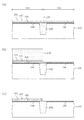
次に、図2(a)に示すように、nチャネル領域103の第1ゲート電極材料膜107を覆うように堆積された第2ゲート電極膜111の上に、nチャネル領域103を開口したレジストパターン112を形成した後、レジストパターン112をマスクとして、第2ゲート電極材料膜111つまりTiN膜に対してエッチングを行い、nチャネル領域103上に位置する部分の第2ゲート電極材料膜111を除去する。第2ゲート電極材料膜111であるTiN膜は、例えばSPM溶液、希釈塩酸若しくは過酸化水素水等の薬液、又は低ダメージのリモートプラズマを用いたケミカルドライエッチングによって除去することが可能である。或いは、例えばRIEによるドライエッチングを用いてnチャネル領域103の第2ゲート電極材料膜111を選択的に除去し、当該エッチングを第1ゲート電極材料膜107の表面でストップさせてもよい。このRIEによるドライエッチングを用いた場合には、np境界110におけるレジストパターン112の側面からpチャネル領域104上の第2ゲート電極材料膜111が後退する量を低減することができる。尚、第2ゲート電極材料膜111のエッチングの実施後、例えばSPM溶液又はシンナー溶液等を用いてレジストパターン112を除去する。
Next, as shown in FIG. 2A, a resist in which the n-
次に、図2(b)に示すように、半導体基板101上の全面に第3ゲート電極材料膜113として、例えばP(燐)をドーピングした厚さ80nm〜150nm程度のポリシリコン膜を堆積した後、第3ゲート電極材料膜113の上に、nチャネル領域103及びpチャネル領域104のそれぞれのゲート電極形成領域を覆うレジストパターン114をフォトリソグラフィにより形成する。このとき、オーバーエッチング吸収層となる第1ゲート電極材料膜107の存在により、nチャネル領域103におけるnチャネルゲート電極高さ115とpチャネル領域104におけるpチャネルゲート電極高さ116との差が小さくなっているため、レジストパターン114を形成する際のフォーカスマージンが拡大するので、レジストパターン114として、より微細なパターンを形成することが可能となる。
Next, as shown in FIG. 2B, a polysilicon film having a thickness of about 80 nm to 150 nm doped with, for example, P (phosphorus) is deposited as a third gate
次に、レジストパターン114をマスクとして、nチャネル領域103上における第3ゲート電極材料膜113と第1ゲート電極材料膜107との積層膜、及びpチャネル領域104における第3ゲート電極材料膜113と第2ゲート電極材料膜111との積層膜に対して同時に、例えばハロゲン系のエッチングガスを用いた異方性ドライエッチングを行い、その後、レジストパターン114を除去する。これにより、図2(c)に示すように、nチャネル領域103上には、ゲート絶縁膜と接する第1ゲート電極材料膜(ポリシリコン膜)107と、その上に形成された第3ゲート電極材料膜(ポリシリコン膜)113とからなるゲート電極151が形成されると共に、pチャネル領域104上には、ゲート絶縁膜と接する第2ゲート電極材料膜(TiN膜)111と、その上に形成された第3ゲート電極材料膜(ポリシリコン膜)113とからなるゲート電極152が形成される。このとき、nチャネル領域103及びpチャネル領域104に共通に形成されている第3ゲート電極材料膜113についてはnチャネル領域103及びpチャネル領域104のそれぞれにおいて同時にエッチングが完了する。また、第3ゲート電極材料膜113のエッチングに引き続き、nチャネル領域103の第1ゲート電極材料膜107とpチャネル領域104の第2ゲート電極材料膜111とに対して同時にエッチングが実施される。ここで、前述したように、オーバーエッチング吸収層となる第1ゲート電極材料膜107の膜厚は、pチャネル領域104のトランジスタの閾値制御を行うための第2ゲート電極材料111の膜厚、及びゲート加工での各ゲート電極材料膜のエッチングレート比に応じて、第1ゲート電極材料膜107及び第2ゲート電極材料膜111のそれぞれのエッチングが完了する時間が実質的に同じとなるように予め設定されている。従って、nチャネル領域103及びpチャネル領域104のそれぞれにおいて第1ゲート電極材料膜107のエッチングと第2ゲート電極材料膜111のエッチングとは同時に完了する。これにより、nチャネル領域103及びpチャネル領域104のそれぞれにおいてゲート絶縁膜105に対するオーバーエッチング量を揃えることが可能となるため、ゲート絶縁膜105に対する過剰なオーバーエッチングは発生しない。従って、ゲート絶縁膜105の突き抜けやそれに伴う半導体基板101の削れ等の問題は発生しない。
Next, using the resist
次に、図3(a)に示すように、nチャネル領域103上及びpチャネル領域104上の全面に、例えばLP−CVD(low pressure-chemical vapor deposition)法によりTEOS(tetraethylorthosilicate )膜又はSiN膜などの絶縁膜を厚さ5〜20nm程度堆積した後、当該絶縁膜に対して異方性ドライエッチングによるエッチバックを行って、ゲート電極151及び152のそれぞれの側面にオフセットスペーサ117を形成する。次に、ゲート電極151及び152並びにオフセットスペーサ117をマスクとして、nチャネル領域103及びpチャネル領域104のそれぞれに対してイオン注入を行うことにより、nチャネル領域103におけるゲート電極151の両側にエクステンション注入層118Aを形成すると共にpチャネル領域104におけるゲート電極152の両側にエクステンション注入層118Bを形成する。
Next, as shown in FIG. 3A, a TEOS (tetraethylorthosilicate) film or a SiN film is formed on the entire surface of the n-
次に、図3(b)に示すように、nチャネル領域103上及びpチャネル領域104上の全面に、例えばSA−CVD(sub atmospheric-chemical vapor deposiition)法によりNSG(nondoped silicate glass )膜を厚さ5〜10nm程度堆積した後、例えばALD(atomic layer deposition )法によりSiN膜を厚さ20〜40nm程度堆積する。次に、NSG膜とSiN膜との積層膜に対して異方性ドライエッチングによるエッチバックを行って、ゲート電極151及び152のそれぞれの側面にオフセットスペーサ117を介して、サイドウォール下層膜119及びサイドウォール上層膜120からなるサイドウォールスペーサ121を形成する。尚、サイドウォール下層膜119として、NSG膜に代えて、例えばLP−CVD法によりTEOS膜を形成してもよい。次に、ゲート電極151、オフセットスペーサ117及びサイドウォールスペーサ121をマスクとして、nチャネル領域103に対してAs(砒素)及びP(燐)のイオン注入を行うことにより、nチャネル領域103におけるゲート電極151から見てエクステンション注入層118Aの外側にソース・ドレイン注入層122Aを形成する。また、ゲート電極152、オフセットスペーサ117及びサイドウォールスペーサ121をマスクとして、pチャネル領域104に対してB(ホウ素)のイオン注入を行うことにより、pチャネル領域104におけるゲート電極152から見てエクステンション注入層118Bの外側にソース・ドレイン注入層122Bを形成する。その後、活性化熱処理を行い、イオン注入によって半導体基板101中に導入した各不純物を活性化する。
Next, as shown in FIG. 3B, an NSG (nondoped silicate glass) film is formed on the entire surface of the n-
次に、nチャネル領域103上及びpチャネル領域104上の全面に、高融点金属膜として例えばNi膜をスパッタ法などによって堆積した後、シリサイド化熱処理を実施し、その後、シリサイド未反応領域のNi膜を例えばウェットエッチングにより除去する。これにより、図3(c)に示すように、ソース・ドレイン注入層122A及び122Bのそれぞれの表面並びにゲート電極151及び152のそれぞれの表面にNiシリサイド層124が形成される。
Next, after depositing, for example, a Ni film as a refractory metal film on the entire surface of the n-
以上に説明した第1の実施形態によると、ゲート絶縁膜105と接する第2ゲート電極材料膜(TiN膜)111がゲート電極151の一部として形成されないnチャネル領域103上に、第2ゲート電極材料膜(TiN膜)111のエッチング時にオーバーエッチング吸収層として機能する第1ゲート電極材料膜(ポリシリコン膜)107を予め形成している。このため、第2ゲート電極材料膜(TiN膜)111のエッチング時にゲート絶縁膜105に対するオーバーエッチング量が各トランジスタ領域で実質的に同等となるように第1ゲート電極材料膜(ポリシリコン膜)107の膜厚等を設定することにより、各トランジスタ領域間でのゲート絶縁膜105に対するオーバーエッチング量の不均一性を低減できる。従って、ゲート絶縁膜105の突き抜け及びそれに伴う基板削れ等を防止できるため、トランジスタ特性劣化やパーティクル増加等に起因する歩留まり低下の危険を回避でき、それによって高性能な半導体装置を安価で提供することができる。
According to the first embodiment described above, the second gate electrode is formed on the n-
また、第1の実施形態によると、ゲート電極加工時のエッチングにおけるオーバーエッチング量が各トランジスタ領域において実質的に同等となるため、オーバーエッチングに伴うゲート寸法変化を各トランジスタ領域で揃えることができる。このため、各トランジスタ、具体的にはnチャネル型電界効果トランジスタ及びpチャネル型電界効果トランジスタのそれぞれにおけるゲート寸法のばらつきを低減することが可能となり、トランジスタ特性がより安定した半導体装置を提供することができる。 In addition, according to the first embodiment, the amount of overetching in the etching at the time of processing the gate electrode is substantially equal in each transistor region, so that the gate dimension change due to overetching can be made uniform in each transistor region. Therefore, it is possible to reduce variations in gate dimensions of each transistor, specifically, an n-channel field effect transistor and a p-channel field effect transistor, and provide a semiconductor device with more stable transistor characteristics. Can do.
(第1の実施形態の第1変形例)
以下、本発明の第1の実施形態の第1変形例に係る半導体装置及びその製造方法について、図面を参照しながら説明する。
(First modification of the first embodiment)
Hereinafter, a semiconductor device and a manufacturing method thereof according to a first modification of the first embodiment of the present invention will be described with reference to the drawings.
図4(a)〜(c)及び図5(a)〜(c)は、本発明の第1の実施形態の第1変形例に係る半導体装置の製造方法の各工程を示す断面図である。尚、図4(a)〜(c)及び図5(a)〜(c)において、図1(a)〜(c)、図2(a)〜(c)及び図3(a)〜(c)に示す第1の実施形態と同一の構成要素には同一の符号を付すことにより、重複する説明を省略する。 FIGS. 4A to 4C and FIGS. 5A to 5C are cross-sectional views showing respective steps of the method for manufacturing a semiconductor device according to the first modification of the first embodiment of the present invention. . 4A to 4C and FIGS. 5A to 5C, FIGS. 1A to 1C, FIGS. 2A to 2C, and FIGS. The same components as those in the first embodiment shown in c) are denoted by the same reference numerals, and redundant description is omitted.
まず、図4(a)に示すように、半導体基板101に例えばSTIからなる素子分離102を形成し、nチャネル領域103及びpチャネル領域104を区画した後、nチャネル領域103及びpチャネル領域104のそれぞれに対してウェル形成用イオン注入を実施する。次に、nチャネル領域103及びpチャネル領域104のそれぞれに対して、トランジスタの閾値を調整するためのイオン注入を実施する。次に、例えばロジックトランジスタ、SRAMトランジスタ、及び入出力I/Oトランジスタ等の各トランジスタの機能に応じた膜厚及び膜質を持つゲート絶縁膜の作りこみを実施する。図4(a)は、nチャネル領域103及びpチャネル領域104のそれぞれの上に、例えばロジックトランジスタ用のゲート絶縁膜105を形成している場合を示している。具体的には、ゲート絶縁膜105は、半導体基板101の表面に形成された、シリコン酸化膜と比較して比誘電率の十分に高い高誘電率膜、例えばハフニウムシリコン酸化膜(HfSix Oy 膜)である。ここで、HfSix Oy 膜のEOTは約2.0nmである。尚、ゲート絶縁膜105と半導体基板101との界面には、半導体基板101が酸化されてなる例えば厚さ1nm程度の極薄シリコン酸化膜が界面層106として形成されている。
First, as shown in FIG. 4A, an
次に、図4(a)に示すように、ゲート絶縁膜105の直上に、nチャネル領域103のトランジスタの閾値制御を行うための第1ゲート電極材料膜107として、例えばP(燐)をドーピングした厚さ5〜20nm程度のポリシリコン膜を堆積する。この第1ゲート電極材料膜107はオーバーエッチング吸収層として機能するものであり、後の工程で実施されるゲート電極加工時のドライエッチングにおいて、ゲート絶縁膜105へのオーバーエッチング量がnチャネル領域103及びpチャネル領域104で実質的に同等となるように、膜厚等が設定されている。
Next, as shown in FIG. 4A, for example, P (phosphorus) is doped immediately above the
次に、図4(a)に示すように、第1ゲート電極材料膜107の上に、例えばHDP−NSG(high density plasma-nondoped silicate glass )からなる第1エッチングカバー膜201を形成する。
Next, as shown in FIG. 4A, a first
次に、図4(b)に示すように、第1エッチングカバー膜201の上に、pチャネル領域104を開口したレジストパターン109を形成した後、レジストパターン109をマスクとして異方性ドライエッチングを行うことにより、pチャネル領域104上に位置する部分の第1エッチングカバー膜201を除去すると共にpチャネル領域104上に位置する部分の第1ゲート電極材料膜107を途中まで除去する。その後、レジストパターン109を除去する。
Next, as shown in FIG. 4B, a resist
次に、図4(c)に示すように、nチャネル領域103を覆う第1エッチングカバー膜201をマスクとして、pチャネル領域104上に残存する第1ゲート電極材料膜107を除去する。ここで、第1ゲート電極材料膜107であるポリシリコン膜のエッチングには、例えば65℃に加熱した水酸化カリウム溶液(KOH/H2 O=0.3g/150cc)を用いる。これにより、ゲート絶縁膜105の膜減り等のダメージを防止しながらエッチングを行うことができる。或いは、例えば80℃に加熱した希釈APM溶液(NH3 :H2 O2 :H2 O=3〜10:1:200〜1000)又は低ダメージのリモートプラズマを用いたケミカルドライエッチングによって第1ゲート電極材料膜107を除去することも可能である。
Next, as shown in FIG. 4C, the first gate
本変形例においては、第1エッチングカバー膜201をマスクとして、第1ゲート電極材料膜107のエッチングを行うため、エッチングを実施した後に基板表面がその他の薬液などに曝されることがないので、ゲート絶縁膜105の表面にダメージ等が生じることはない。
In this modification, since the first gate
次に、図5(a)に示すように、pチャネル領域104のトランジスタの閾値制御を行うための第2ゲート電極材料膜111として、例えば厚さ5〜20nm程度のTiN膜をnチャネル領域103上及びpチャネル領域104上のそれぞれの全面に堆積する。
Next, as shown in FIG. 5A, as the second gate
このとき、前述のオーバーエッチング吸収層となる第1ゲート電極材料膜107の膜厚は、pチャネル領域104のトランジスタの閾値制御を行うための第2ゲート電極材料111の膜厚、及びゲート加工での各ゲート電極材料膜のエッチングレート比に応じて、第1ゲート電極材料膜107及び第2ゲート電極材料膜111のそれぞれのエッチングが完了する時間が実質的に同じになるように予め設定されている。オーバーエッチング吸収層となる第1ゲート電極材料膜107の膜厚の具体的な決定は、第1の実施形態で説明した(式1)〜(式3)に従って行われる。
At this time, the film thickness of the first gate
次に、図5(b)に示すように、第2ゲート電極膜111の上に、nチャネル領域103を開口したレジストパターン112を形成した後、nチャネル領域103の第1エッチングカバー膜201、及びレジストパターン112をマスクとして、第2ゲート電極材料膜111つまりTiN膜に対してエッチングを行い、nチャネル領域103上に位置する部分の第2ゲート電極材料膜111を除去する。このとき、第2ゲート電極材料膜111であるTiN膜を、例えばRIEによるドライエッチングを用いて除去することが可能である。或いは、例えばSPM溶液、希釈塩酸若しくは過酸化水素水等の薬液、又は低ダメージのリモートプラズマを用いたケミカルドライエッチングによって、第2ゲート電極材料膜111であるTiN膜を除去することも可能である。第2ゲート電極材料膜111のエッチングの実施後、例えばSPM溶液又はシンナー溶液等を用いてレジストパターン112を除去する。続いて、第1エッチングカバー膜201であるHDP−NSG膜を、例えば異方性ドライエッチング、又はHF薬液(フッ酸)等を用いたウェットエッチングにより除去する。
Next, as shown in FIG. 5B, after forming a resist
本変形例においては、第2ゲート電極材料膜111をエッチングする際に、nチャネル領域103上においては第1エッチングカバー膜201がストッパーとなるため、その下側に存在する第1ゲート電極材料膜107の表面はエッチングされることがない。
In the present modification, when the second gate
次に、図5(c)に示すように、半導体基板101上の全面に第3ゲート電極材料膜113として、例えばP(燐)をドーピングした厚さ80nm〜150nm程度のポリシリコン膜を堆積した後、第3ゲート電極材料膜113の上に、nチャネル領域103及びpチャネル領域104のそれぞれのゲート電極形成領域を覆うレジストパターン114をフォトリソグラフィにより形成する。このとき、オーバーエッチング吸収層となる第1ゲート電極材料膜107の存在により、nチャネル領域103におけるnチャネルゲート電極高さ115とpチャネル領域104におけるpチャネルゲート電極高さ116との差が小さくなっているため、レジストパターン114を形成する際のフォーカスマージンが拡大するので、レジストパターン114として、より微細なパターンを形成することが可能となる。
Next, as shown in FIG. 5C, a polysilicon film having a thickness of about 80 nm to 150 nm doped with P (phosphorus), for example, is deposited as the third gate
その後、第1の実施形態の図2(c)及び図3(a)〜(c)に示す各工程と同様の工程を実施することにより、第1の実施形態と同様の構造を持つ半導体装置を得ることができる。 Thereafter, by performing the same steps as the steps shown in FIG. 2C and FIGS. 3A to 3C of the first embodiment, a semiconductor device having the same structure as that of the first embodiment Can be obtained.
以上に説明した第1の実施形態の第1変形例によると、第1の実施形態と同様に、ゲート絶縁膜105と接する第2ゲート電極材料膜(TiN膜)111がゲート電極151の一部として形成されないnチャネル領域103上に、第2ゲート電極材料膜(TiN膜)111のエッチング時にオーバーエッチング吸収層として機能する第1ゲート電極材料膜(ポリシリコン膜)107を予め形成している。このため、第2ゲート電極材料膜(TiN膜)111のエッチング時にゲート絶縁膜105に対するオーバーエッチング量が各トランジスタ領域で実質的に同等となるように第1ゲート電極材料膜(ポリシリコン膜)107の膜厚等を設定することにより、各トランジスタ領域間でのゲート絶縁膜105に対するオーバーエッチング量の不均一性を低減できる。従って、ゲート絶縁膜105の突き抜け及びそれに伴う基板削れ等を防止できるため、トランジスタ特性劣化やパーティクル増加等に起因する歩留まり低下の危険を回避でき、それによって高性能な半導体装置を安価で提供することができる。
According to the first modification of the first embodiment described above, the second gate electrode material film (TiN film) 111 in contact with the
また、第1の実施形態の第1変形例によると、ゲート電極加工時のエッチングにおけるオーバーエッチング量が各トランジスタ領域において実質的に同等となるため、オーバーエッチングに伴うゲート寸法変化を各トランジスタ領域で揃えることができる。このため、各トランジスタ、具体的にはnチャネル型電界効果トランジスタ及びpチャネル型電界効果トランジスタのそれぞれにおけるゲート寸法のばらつきを低減することが可能となり、トランジスタ特性がより安定した半導体装置を提供することができる。 Further, according to the first modification of the first embodiment, the overetching amount in the etching at the time of processing the gate electrode is substantially equal in each transistor region. Can be aligned. Therefore, it is possible to reduce variations in gate dimensions of each transistor, specifically, an n-channel field effect transistor and a p-channel field effect transistor, and provide a semiconductor device with more stable transistor characteristics. Can do.
さらに、第1の実施形態の第1変形例によると、第1エッチングカバー膜201をハードマスクとして第1ゲート電極材料107であるポリシリコン膜のエッチングを実施するため、エッチングを実施した後に基板表面がその他の薬液などに曝されることがないので、ゲート絶縁膜105の表面にダメージ等が生じる危険を回避することができる。
Furthermore, according to the first modification of the first embodiment, the polysilicon film that is the first
また、第1の実施形態の第1変形例によると、nチャネル領域103上に形成された第2ゲート電極材料膜111であるTiN膜をエッチングにより除去する際に、第1エッチングカバー膜201がエッチングストッパーとして機能するため、第1エッチングカバー膜201の下側に存在する第1ゲート電極材料膜107の表面がエッチングされることがないので、nチャネル領域103上における膜減り等の発生を防止することができる。
Further, according to the first modification of the first embodiment, when the TiN film, which is the second gate
(第1の実施形態の第2変形例)
以下、本発明の第1の実施形態の第2変形例に係る半導体装置及びその製造方法について、図面を参照しながら説明する。
(Second modification of the first embodiment)
Hereinafter, a semiconductor device and a manufacturing method thereof according to a second modification of the first embodiment of the present invention will be described with reference to the drawings.
図6(a)、(b)及び図7(a)、(b)は、本発明の第1の実施形態の第2変形例に係る半導体装置の製造方法の各工程を示す断面図である。尚、図6(a)、(b)及び図7(a)、(b)において、図1(a)〜(c)、図2(a)〜(c)及び図3(a)〜(c)に示す第1の実施形態、又は図4(a)〜(c)及び図5(a)〜(c)に示す第1の実施形態の第1変形例と同一の構成要素には同一の符号を付すことにより、重複する説明を省略する。 6 (a), 6 (b), 7 (a), and 7 (b) are cross-sectional views showing respective steps of a method for manufacturing a semiconductor device according to a second modification of the first embodiment of the present invention. . 6A, 6B, 7A, and 7B, FIGS. 1A to 1C, 2A to 2C, and 3A to 3B. The same components as those of the first embodiment shown in c) or the first modification of the first embodiment shown in FIGS. 4 (a) to 4 (c) and FIGS. 5 (a) to 5 (c) are the same. The description which overlaps is abbreviate | omitted.
まず、本変形例においては、図4(a)〜(c)に示す第1の実施形態の第1変形例の各工程と同様の工程を順次実施する。 First, in this modification, the same processes as those in the first modification of the first embodiment shown in FIGS. 4A to 4C are sequentially performed.
次に、図6(a)に示すように、pチャネル領域104のトランジスタの閾値制御を行うための第2ゲート電極材料膜111として、例えば厚さ5〜20nm程度のTiN膜をnチャネル領域103上及びpチャネル領域104上のそれぞれの全面に堆積する。
Next, as shown in FIG. 6A, for example, a TiN film having a thickness of about 5 to 20 nm is formed as the second gate
このとき、前述のオーバーエッチング吸収層となる第1ゲート電極材料膜107の膜厚は、pチャネル領域104のトランジスタの閾値制御を行うための第2ゲート電極材料111の膜厚、及びゲート加工での各ゲート電極材料膜のエッチングレート比に応じて、第1ゲート電極材料膜107及び第2ゲート電極材料膜111のそれぞれのエッチングが完了する時間が実質的に同じになるように予め設定されている。オーバーエッチング吸収層となる第1ゲート電極材料膜107の膜厚の具体的な決定は、第1の実施形態で説明した(式1)〜(式3)に従って行われる。
At this time, the film thickness of the first gate
次に、図6(a)に示すように、第2ゲート電極材料膜111の上に、例えばHDP−NSGからなる第2エッチングカバー膜301を形成する。
Next, as shown in FIG. 6A, a second
次に、図6(b)に示すように、第2エッチングカバー膜301の上に、nチャネル領域103を開口したレジストパターン112を形成した後、nチャネル領域103上に位置する部分の第2エッチングカバー膜301及び第2ゲート電極材料膜111つまりTiN膜を順次エッチングにより除去する。このとき、第2エッチングカバー膜301であるHDP−NSG膜及び第2ゲート電極材料膜111であるTiN膜を、例えばRIEによるドライエッチングを用いて除去することが可能である。或いは、例えばHF薬液(フッ酸)を用いて第2エッチングカバー膜301であるHDP−NSG膜をエッチング除去した後に、例えばSPM溶液、希釈塩酸若しくは過酸化水素水等の薬液、又は低ダメージのリモートプラズマを用いたケミカルドライエッチングによって、第2ゲート電極材料膜111であるTiN膜を除去することも可能である。第2エッチングカバー膜301及び第2ゲート電極材料膜111のエッチングの実施後、例えばSPM溶液又はシンナー溶液等を用いてレジストパターン112を除去する。
Next, as shown in FIG. 6B, a resist
本変形例においては、第2エッチングカバー膜301及び第2ゲート電極材料膜111をエッチングする際に、nチャネル領域103上においては第1エッチングカバー膜201がストッパーとなるため、その下側に存在する第1ゲート電極材料膜107の表面はエッチングされることがない。
In this modification, when the second
続いて、図7(a)に示すように、nチャネル領域103上に残存する第1エッチングカバー膜201であるHDP−NSG膜、及びpチャネル領域104上に残存する第2エッチングカバー膜301であるHDP−NSG膜を、例えば異方性ドライエッチング、又はHF薬液(フッ酸)等を用いたウェットエッチングにより除去する。
Subsequently, as shown in FIG. 7A, the HDP-NSG film which is the first
次に、図7(b)に示すように、半導体基板101上の全面に第3ゲート電極材料膜113として、例えばP(燐)をドーピングした厚さ80nm〜150nm程度のポリシリコン膜を堆積した後、第3ゲート電極材料膜113の上に、nチャネル領域103及びpチャネル領域104のそれぞれのゲート電極形成領域を覆うレジストパターン114をフォトリソグラフィにより形成する。このとき、オーバーエッチング吸収層となる第1ゲート電極材料膜107の存在により、nチャネル領域103におけるnチャネルゲート電極高さ115とpチャネル領域104におけるpチャネルゲート電極高さ116との差が小さくなっているため、レジストパターン114を形成する際のフォーカスマージンが拡大するので、レジストパターン114として、より微細なパターンを形成することが可能となる。
Next, as shown in FIG. 7B, a polysilicon film having a thickness of about 80 nm to 150 nm doped with P (phosphorus), for example, is deposited on the entire surface of the
その後、第1の実施形態の図2(c)及び図3(a)〜(c)に示す各工程と同様の工程を実施することにより、第1の実施形態と同様の構造を持つ半導体装置を得ることができる。 Thereafter, by performing the same steps as the steps shown in FIG. 2C and FIGS. 3A to 3C of the first embodiment, a semiconductor device having the same structure as that of the first embodiment Can be obtained.
以上に説明した第1の実施形態の第2変形例によると、第1の実施形態と同様に、ゲート絶縁膜105と接する第2ゲート電極材料膜(TiN膜)111がゲート電極151の一部として形成されないnチャネル領域103上に、第2ゲート電極材料膜(TiN膜)111のエッチング時にオーバーエッチング吸収層として機能する第1ゲート電極材料膜(ポリシリコン膜)107を予め形成している。このため、第2ゲート電極材料膜(TiN膜)111のエッチング時にゲート絶縁膜105に対するオーバーエッチング量が各トランジスタ領域で実質的に同等となるように第1ゲート電極材料膜(ポリシリコン膜)107の膜厚等を設定することにより、各トランジスタ領域間でのゲート絶縁膜105に対するオーバーエッチング量の不均一性を低減できる。従って、ゲート絶縁膜105の突き抜け及びそれに伴う基板削れ等を防止できるため、トランジスタ特性劣化やパーティクル増加等に起因する歩留まり低下の危険を回避でき、それによって高性能な半導体装置を安価で提供することができる。
According to the second modification of the first embodiment described above, the second gate electrode material film (TiN film) 111 in contact with the
また、第1の実施形態の第2変形例によると、ゲート電極加工時のエッチングにおけるオーバーエッチング量が各トランジスタ領域において実質的に同等となるため、オーバーエッチングに伴うゲート寸法変化を各トランジスタ領域で揃えることができる。このため、各トランジスタ、具体的にはnチャネル型電界効果トランジスタ及びpチャネル型電界効果トランジスタのそれぞれにおけるゲート寸法のばらつきを低減することが可能となり、トランジスタ特性がより安定した半導体装置を提供することができる。 In addition, according to the second modification of the first embodiment, the amount of overetching in etching at the time of gate electrode processing is substantially equal in each transistor region. Can be aligned. Therefore, it is possible to reduce variations in gate dimensions of each transistor, specifically, an n-channel field effect transistor and a p-channel field effect transistor, and provide a semiconductor device with more stable transistor characteristics. Can do.
さらに、第1の実施形態の第2変形例によると、第1エッチングカバー膜201をハードマスクとして第1ゲート電極材料107であるポリシリコン膜のエッチングを実施するため、エッチングを実施した後に基板表面がその他の薬液などに曝されることがないので、ゲート絶縁膜105の表面にダメージ等が生じる危険を回避することができる。
Furthermore, according to the second modification of the first embodiment, since the polysilicon film as the first
また、第1の実施形態の第2変形例によると、nチャネル領域103上に形成された第2ゲート電極材料膜111であるTiN膜をエッチングにより除去する際に、第1エッチングカバー膜201がエッチングストッパーとして機能するため、第1エッチングカバー膜201の下側に存在する第1ゲート電極材料膜107の表面がエッチングされることがないので、nチャネル領域103上における膜減り等の発生を防止することができる。
Further, according to the second modification of the first embodiment, when the TiN film, which is the second gate
また、第1の実施形態の第2変形例によると、第2ゲート電極材料膜111上にレジストパターン112をパターニング形成する際に、第2エッチングカバー膜301が第2ゲート電極材料膜111とレジストパターン112との間に存在している。このため、第2ゲート電極材料膜111の直上にレジストパターン112をパターニング形成する場合のように、第2ゲート電極材料膜111が金属含有材料からなることに起因してレジスト失活等が起こり、その影響を受けてレジスト裾引きが発生する等の危険を回避することができる。
Further, according to the second modification of the first embodiment, when the resist
(第1の実施形態の第3変形例)
以下、本発明の第1の実施形態の第3変形例に係る半導体装置及びその製造方法について、図面を参照しながら説明する。
(Third Modification of First Embodiment)
Hereinafter, a semiconductor device and a manufacturing method thereof according to a third modification of the first embodiment of the present invention will be described with reference to the drawings.
図26(a)〜(c)、図27(a)〜(c)及び図28(a)〜(c)は、本発明の第1の実施形態の第3変形例に係る半導体装置の製造方法の各工程を示す断面図である。尚、図26(a)〜(c)、図27(a)〜(c)及び図28(a)〜(c)において、図1(a)〜(c)、図2(a)〜(c)及び図3(a)〜(c)に示す第1の実施形態と同一の構成要素には同一の符号を付すことにより、重複する説明を省略する。 FIGS. 26A to 26C, FIGS. 27A to 27C, and FIGS. 28A to 28C illustrate the manufacture of the semiconductor device according to the third modification of the first embodiment of the present invention. It is sectional drawing which shows each process of a method. 26 (a) to (c), FIGS. 27 (a) to (c) and FIGS. 28 (a) to (c), FIGS. 1 (a) to (c) and FIGS. The same components as those in the first embodiment shown in c) and FIGS. 3A to 3C are denoted by the same reference numerals, and redundant description is omitted.
まず、第1の実施形態の図1(a)に示す工程と同様に、図26(a)に示す工程を実施する。ここで、本変形例が第1の実施形態と異なっている点は、第1ゲート電極材料膜107として堆積するポリシリコン膜の厚さが10〜40nm程度であり、後述する図26(c)に示す工程(第1の実施形態の図1(c)に示す工程に相当)で第2ゲート電極材料膜111として堆積される金属膜の厚さ(5〜20nm程度)よりも2倍程度大きいことである。尚、本変形例では、この金属膜として、例えば、Ta系金属膜であるTaN膜若しくはTaCN膜、又は酸素含有金属膜であるTiON膜、TiCNO膜、TaCO膜若しくはTaCNO膜等を用いる。
First, similarly to the step shown in FIG. 1A of the first embodiment, the step shown in FIG. Here, this modification is different from the first embodiment in that the thickness of the polysilicon film deposited as the first gate
続いて、第1の実施形態の図1(b)、(c)、図2(a)〜(c)及び図3(a)〜(c)に示す工程と同様に、図26(b)、(c)、図27(a)〜(c)及び図28(a)〜(c)に示す工程を順次実施する。ここで、前述のように、第1の実施形態と比べて第1ゲート電極材料膜107の厚さが大きい点を除いて、各工程の内容は第1の実施形態の対応する工程と同じである。
Subsequently, similarly to the steps shown in FIGS. 1B and 1C, FIGS. 2A to 2C and FIGS. 3A to 3C of the first embodiment, FIG. , (C), steps (a) to (c) and steps (a) to (c) shown in FIG. Here, as described above, the contents of each step are the same as the corresponding steps of the first embodiment except that the thickness of the first gate
以上に説明した第1の実施形態の第3変形例においても、第1の実施形態と同様の効果を得ることができる。 Also in the third modified example of the first embodiment described above, the same effect as in the first embodiment can be obtained.
また、本変形例のように、第2ゲート電極材料膜111として、前述のようなTa系金属膜や酸素含有金属膜を用いた場合、これらの金属膜の構成元素間の結合解離エネルギーが、シリコン結合を切断するための結合解離エネルギーよりも大きいため、これらの金属膜のエッチングレートはポリシリコン膜のエッチングレートよりも小さくなる。従って、本変形例のように、第1ゲート電極材料膜107として堆積するポリシリコン膜の厚さを、第2ゲート電極材料膜111として堆積する金属膜の厚さよりも大きくすることが、本発明の効果を得る上で特に有効である。
In addition, when the Ta-based metal film or the oxygen-containing metal film as described above is used as the second gate
(第2の実施形態)
以下、本発明の第2の実施形態に係る半導体装置及びその製造方法について、図面を参照しながら説明する。
(Second Embodiment)
Hereinafter, a semiconductor device and a manufacturing method thereof according to a second embodiment of the present invention will be described with reference to the drawings.
図8(a)〜(c)、図9(a)〜(c)、図10(a)〜(c)及び図11(a)〜(c)は、本発明の第2の実施形態に係る半導体装置の製造方法の各工程を示す断面図である。尚、図8(a)〜(c)、図9(a)〜(c)、図10(a)〜(c)及び図11(a)〜(c)において、図1(a)〜(c)、図2(a)〜(c)及び図3(a)〜(c)に示す第1の実施形態と同一の構成要素には同一の符号を付すことにより、重複する説明を省略する。 8 (a) to (c), FIG. 9 (a) to (c), FIG. 10 (a) to (c) and FIG. 11 (a) to (c) are shown in the second embodiment of the present invention. It is sectional drawing which shows each process of the manufacturing method of the semiconductor device which concerns. 8 (a) to (c), FIGS. 9 (a) to (c), FIGS. 10 (a) to (c) and FIGS. 11 (a) to 11 (c), FIGS. c) The same components as those in the first embodiment shown in FIGS. 2A to 2C and FIGS. 3A to 3C are denoted by the same reference numerals, and redundant description is omitted. .
まず、図8(a)に示すように、半導体基板101に例えばSTIからなる素子分離102を形成し、nチャネル領域103及びpチャネル領域104を区画した後、nチャネル領域103及びpチャネル領域104のそれぞれに対してウェル形成用イオン注入を実施する。次に、nチャネル領域103及びpチャネル領域104のそれぞれに対して、トランジスタの閾値を調整するためのイオン注入を実施する。次に、例えばロジックトランジスタ、SRAMトランジスタ、及び入出力I/Oトランジスタ等の各トランジスタの機能に応じた膜厚及び膜質を持つゲート絶縁膜の作りこみを実施する。図8(a)は、nチャネル領域103及びpチャネル領域104のそれぞれの上に、例えばロジックトランジスタ用のゲート絶縁膜105を形成している場合を示している。具体的には、ゲート絶縁膜105は、半導体基板101の表面に形成された、シリコン酸化膜と比較して比誘電率の十分に高い高誘電率膜、例えばハフニウムシリコン酸化膜(HfSix Oy 膜)である。ここで、HfSix Oy 膜のEOTは約2.0nmである。尚、ゲート絶縁膜105と半導体基板101との界面には、半導体基板101が酸化されてなる例えば厚さ1nm程度の極薄シリコン酸化膜が界面層106として形成されている。
First, as shown in FIG. 8A, an
次に、図8(a)に示すように、ゲート絶縁膜105の直上に、nチャネル領域103のトランジスタの閾値制御を行うための第1ゲート電極材料膜107として、例えばP(燐)をドーピングした厚さ5〜20nm程度のポリシリコン膜を堆積する。この第1ゲート電極材料膜107はオーバーエッチング吸収層として機能するものであり、後の工程で実施されるゲート電極加工時のドライエッチングにおいて、ゲート絶縁膜105へのオーバーエッチング量がnチャネル領域103及びpチャネル領域104で実質的に同等となるように、膜厚等が設定されている。
Next, as shown in FIG. 8A, for example, P (phosphorus) is doped directly on the
次に、図8(a)に示すように、第1ゲート電極材料膜107の上に、例えば、導電性酸化物であるRu(ルテニウム)酸化物又はIr(イリジウム)酸化物などからなる第1エッチングストッパー膜401を形成する。
Next, as shown in FIG. 8A, on the first gate
次に、図8(b)に示すように、第1エッチングストッパー膜401の上に、pチャネル領域104を開口したレジストパターン109を形成した後、レジストパターン109をマスクとして異方性ドライエッチングを行うことにより、pチャネル領域104上に位置する部分の第1エッチングストッパー膜401を除去すると共にpチャネル領域104上に位置する部分の第1ゲート電極材料膜107を途中まで除去する。その後、レジストパターン109を除去する。
Next, as shown in FIG. 8B, a resist
次に、図8(c)に示すように、nチャネル領域103を覆う第1エッチングストッパー膜401をマスクとして、pチャネル領域104上に残存する第1ゲート電極材料膜107を除去する。ここで、第1ゲート電極材料膜107であるポリシリコン膜のエッチングには、例えば65℃に加熱した水酸化カリウム溶液(KOH/H2 O=0.3g/150cc)を用いる。これにより、ゲート絶縁膜105の膜減り等のダメージを防止しながらエッチングを行うことができる。或いは、例えば80℃に加熱した希釈APM溶液(NH3 :H2 O2 :H2 O=3〜10:1:200〜1000)又は低ダメージのリモートプラズマを用いたケミカルドライエッチングによって第1ゲート電極材料膜107を除去することも可能である。
Next, as shown in FIG. 8C, the first gate
本実施形態においては、第1エッチングストッパー膜401をマスクとして、第1ゲート電極材料膜107のエッチングを行うため、エッチングを実施した後に基板表面がその他の薬液などに曝されることがないので、ゲート絶縁膜105の表面にダメージ等が生じることはない。
In this embodiment, since the first gate
次に、図9(a)に示すように、pチャネル領域104のトランジスタの閾値制御を行うための第2ゲート電極材料膜111として、例えば厚さ5〜20nm程度のTiN膜をnチャネル領域103上及びpチャネル領域104上のそれぞれの全面に堆積する。
Next, as shown in FIG. 9A, for example, a TiN film having a thickness of about 5 to 20 nm is used as the second gate
このとき、前述のオーバーエッチング吸収層となる第1ゲート電極材料膜107の膜厚は、pチャネル領域104のトランジスタの閾値制御を行うための第2ゲート電極材料111の膜厚、及びゲート加工での各ゲート電極材料膜のエッチングレート比に応じて、第1ゲート電極材料膜107及び第2ゲート電極材料膜111のそれぞれのエッチングが完了する時間が実質的に同じになるように予め設定されている。オーバーエッチング吸収層となる第1ゲート電極材料膜107の膜厚の具体的な決定は、第1の実施形態で説明した(式1)〜(式3)に従って行われる。
At this time, the film thickness of the first gate
次に、図9(a)に示すように、第2ゲート電極材料111の上に、例えば導電性酸化物であるRu(ルテニウム)酸化物又はIr(イリジウム)酸化物などからなる第2エッチストッパー膜402を形成する。
Next, as shown in FIG. 9A, a second etch stopper made of, for example, Ru (ruthenium) oxide or Ir (iridium) oxide, which is a conductive oxide, is formed on the second
次に、図9(b)に示すように、第2エッチストッパー膜402の上に、nチャネル領域103を開口したレジストパターン112を形成した後、nチャネル領域103上に位置する部分の第2エッチストッパー膜402及び第2ゲート電極材料膜111つまりTiN膜を順次エッチングにより除去する。このとき、第2エッチストッパー膜402である導電性酸化物膜及び第2ゲート電極材料膜111であるTiN膜を、例えばRIEによるドライエッチングを用いて除去することが可能である。或いは、例えばHF薬液(フッ酸)を用いて第2エッチストッパー膜402である導電性酸化物膜をエッチング除去した後に、例えばSPM溶液、希釈塩酸若しくは過酸化水素水等の薬液、又は低ダメージのリモートプラズマを用いたケミカルドライエッチングによって、第2ゲート電極材料膜111であるTiN膜を除去することも可能である。第2エッチストッパー膜402及び第2ゲート電極材料膜111のエッチングの実施後、例えばSPM溶液又はシンナー溶液等を用いてレジストパターン112を除去する。
Next, as illustrated in FIG. 9B, a resist
本実施形態においては、第2エッチストッパー膜402及び第2ゲート電極材料膜111をエッチングする際に、nチャネル領域103上においては第1エッチストッパー膜401がストッパーとなるため、その下側に存在する第1ゲート電極材料膜107の表面はエッチングされることがない。
In the present embodiment, when the second
次に、図9(c)に示すように、半導体基板101上の全面に、具体的には、nチャネル領域103の第1エッチストッパー膜401上及びpチャネル領域104の第2エッチストッパー膜402上に、第3ゲート電極材料膜113として、例えばP(燐)をドーピングした厚さ80nm〜150nm程度のポリシリコン膜を堆積した後、第3ゲート電極材料膜113の上に、nチャネル領域103及びpチャネル領域104のそれぞれのゲート電極形成領域を覆うレジストパターン114をフォトリソグラフィにより形成する。このとき、オーバーエッチング吸収層となる第1ゲート電極材料膜107の存在により、nチャネル領域103におけるnチャネルゲート電極高さ115とpチャネル領域104におけるpチャネルゲート電極高さ116との差が小さくなっているため、レジストパターン114を形成する際のフォーカスマージンが拡大するので、レジストパターン114として、より微細なパターンを形成することが可能となる。
Next, as shown in FIG. 9C, specifically on the entire surface of the
次に、図10(a)に示すように、レジストパターン114をマスクとして、第3ゲート電極材料膜113に対して、例えばハロゲン系のエッチングガスを用いた異方性ドライエッチングを行う。このとき、nチャネル領域103及びpチャネル領域104に共通に形成されている第3ゲート電極材料113のエッチングはnチャネル領域103及びpチャネル領域104のそれぞれにおいて同時に完了する。また、第1エッチングストッパー膜401及び第2エッチングストッパー膜402により、第3ゲート電極材料膜113の膜厚ばらつき(素子分離102とそれに隣接する活性領域との間の段差に起因する膜厚ばらつきを含む)の影響は吸収され、第3ゲート電極材料膜113のエッチングが完了した時点で第1エッチングストッパー膜401及び第2エッチングストッパー膜402のそれぞれの表面が露出する。
Next, as shown in FIG. 10A, anisotropic dry etching using, for example, a halogen-based etching gas is performed on the third gate
次に、図10(b)に示すように、レジストパターン114をマスクとして、第1エッチングストッパー膜401及び第2エッチングストッパー膜402に対して、例えばフルオロカーボンガスに代表されるフッ素系のエッチングガスを用いた異方性ドライエッチングを行う。第1エッチングストッパー膜401及び第2エッチングストッパー膜402に対するエッチングは、レジストパターン114の外側の第1ゲート電極材料膜107及び第2ゲート電極材料膜111のそれぞれの表面が露出するまで行う。ここで、導電性酸化物である第1エッチングストッパー膜401とポリシリコンである第1ゲート電極材料膜107との間、及び導電性酸化物である第2エッチングストッパー膜402とTiNである第2ゲート電極材料膜111との間では高いエッチング選択比が得られるので、下地である第1ゲート電極材料膜107及び第2ゲート電極材料膜111をほとんど削ることなく、第1エッチングストッパー膜401及び第2エッチングストッパー膜402のエッチングを行うことができる。
Next, as shown in FIG. 10B, a fluorine-based etching gas typified by, for example, a fluorocarbon gas is applied to the first
次に、レジストパターン114をマスクとして、nチャネル領域103上の第1ゲート電極材料膜107、及びpチャネル領域104上の第2ゲート電極材料膜111に対して同時に、例えばハロゲン系のエッチングガスを用いた異方性ドライエッチングを行い、その後、レジストパターン114を除去する。これにより、図10(c)に示すように、nチャネル領域103上には、ゲート絶縁膜と接する第1ゲート電極材料膜(ポリシリコン膜)107と、その上に形成された第1エッチングストッパー膜(導電性酸化物膜)401と、その上に形成された第3ゲート電極材料膜(ポリシリコン膜)113とからなるゲート電極161が形成されると共に、pチャネル領域104上には、ゲート絶縁膜と接する第2ゲート電極材料膜(TiN膜)111と、その上に形成された第2エッチングストッパー膜(導電性酸化物膜)402と、その上に形成された第3ゲート電極材料膜(ポリシリコン膜)113とからなるゲート電極162が形成される。ここで、前述したように、オーバーエッチング吸収層となる第1ゲート電極材料107の膜厚は、pチャネル領域104のトランジスタの閾値制御を行うための第2ゲート電極材料111の膜厚、及びゲート加工での各ゲート電極材料膜のエッチングレート比に応じて、第1ゲート電極材料膜107及び第2ゲート電極材料膜111のそれぞれのエッチングが完了する時間が実質的に同じとなるように予め設定されている。従って、nチャネル領域103及びpチャネル領域104のそれぞれにおいて第1ゲート電極材料膜107のエッチングと第2ゲート電極材料膜111のエッチングとは同時に完了する。これにより、nチャネル領域103及びpチャネル領域104のそれぞれにおいてゲート絶縁膜105に対するオーバーエッチング量を揃えることが可能となるため、ゲート絶縁膜105に対する過剰なオーバーエッチングは発生しない。従って、ゲート絶縁膜105の突き抜けやそれに伴う半導体基板101の削れ等の問題は発生しない。
Next, using the resist
尚、本実施形態において、ゲート電極161及び162の形成後にレジストパターン114を除去したが、これに代えて、図10(a)に示す第3ゲート電極材料膜113のエッチングが完了した後に、レジストパターン114を除去しても良い。すなわち、図10(b)に示す第1エッチングストッパー膜401及び第2エッチングストッパー膜402のエッチング、並びに図10(c)に示す第1ゲート電極材料膜107及び第2ゲート電極材料膜111のエッチングにおいては、パターニングされた第3ゲート電極材料膜113をマスクとして用いてもよい。
In this embodiment, the resist
次に、図11(a)に示すように、nチャネル領域103上及びpチャネル領域104上の全面に、例えばLP−CVD法によりTEOS膜又はSiN膜などの絶縁膜を厚さ5〜20nm程度堆積した後、当該絶縁膜に対して異方性ドライエッチングによるエッチバックを行って、ゲート電極161及び162のそれぞれの側面にオフセットスペーサ117を形成する。次に、ゲート電極161及び162並びにオフセットスペーサ117をマスクとして、nチャネル領域103及びpチャネル領域104のそれぞれに対してイオン注入を行うことにより、nチャネル領域103におけるゲート電極161の両側にエクステンション注入層118Aを形成すると共にpチャネル領域104におけるゲート電極162の両側にエクステンション注入層118Bを形成する。
Next, as shown in FIG. 11A, an insulating film such as a TEOS film or SiN film is formed on the entire surface of the n-
次に、図11(b)に示すように、nチャネル領域103上及びpチャネル領域104上の全面に、例えばSA−CVD法によりNSG膜を厚さ5〜10nm程度堆積した後、例えばALD法によりSiN膜を厚さ20〜40nm程度堆積する。次に、NSG膜とSiN膜との積層膜に対して異方性ドライエッチングによるエッチバックを行って、ゲート電極161及び162のそれぞれの側面にオフセットスペーサ117を介して、サイドウォール下層膜119及びサイドウォール上層膜120からなるサイドウォールスペーサ121を形成する。尚、サイドウォール下層膜119として、NSG膜に代えて、例えばLP−CVD法によりTEOS膜を形成してもよい。次に、ゲート電極161、オフセットスペーサ117及びサイドウォールスペーサ121をマスクとして、nチャネル領域103に対してAs(砒素)及びP(燐)のイオン注入を行うことにより、nチャネル領域103におけるゲート電極161から見てエクステンション注入層118Aの外側にソース・ドレイン注入層122Aを形成する。また、ゲート電極162、オフセットスペーサ117及びサイドウォールスペーサ121をマスクとして、pチャネル領域104に対してB(ホウ素)のイオン注入を行うことにより、pチャネル領域104におけるゲート電極162から見てエクステンション注入層118Bの外側にソース・ドレイン注入層122Bを形成する。その後、活性化熱処理を行い、イオン注入によって半導体基板101中に導入した各不純物を活性化する。
Next, as shown in FIG. 11B, an NSG film having a thickness of about 5 to 10 nm is deposited on the entire surface of the
次に、nチャネル領域103上及びpチャネル領域104上の全面に、高融点金属膜として例えばNi膜をスパッタ法などによって堆積した後、シリサイド化熱処理を実施し、その後、シリサイド未反応領域のNi膜を例えばウェットエッチングにより除去する。これにより、図11(c)に示すように、ソース・ドレイン注入層122A及び122Bのそれぞれの表面並びにゲート電極161及び162のそれぞれの表面にNiシリサイド層124が形成される。
Next, after depositing, for example, a Ni film as a refractory metal film on the entire surface of the n-
以上に説明した第2の実施形態によると、ゲート絶縁膜105と接する第2ゲート電極材料膜(TiN膜)111がゲート電極161の一部として形成されないnチャネル領域103上に、第2ゲート電極材料膜(TiN膜)111のエッチング時にオーバーエッチング吸収層として機能する第1ゲート電極材料膜(ポリシリコン膜)107を予め形成している。このため、第2ゲート電極材料膜(TiN膜)111のエッチング時にゲート絶縁膜105に対するオーバーエッチング量が各トランジスタ領域で実質的に同等となるように第1ゲート電極材料膜(ポリシリコン膜)107の膜厚等を設定することにより、各トランジスタ領域間でのゲート絶縁膜105に対するオーバーエッチング量の不均一性を低減できる。また、第1ゲート電極材料膜(ポリシリコン膜)107上の第3ゲート電極材料膜(ポリシリコン膜)113のエッチング時にエッチングストッパーとして機能する第1エッチングストッパー膜401を形成しているので、膜厚等が所定値に設定された第1ゲート電極材料膜(ポリシリコン膜)107に膜減り等が生じることもない。従って、ゲート絶縁膜105の突き抜け及びそれに伴う基板削れ等を防止できるため、トランジスタ特性劣化やパーティクル増加等に起因する歩留まり低下の危険を回避でき、それによって高性能な半導体装置を安価で提供することができる。
According to the second embodiment described above, the second gate electrode is formed on the n-
また、第2の実施形態によると、ゲート電極加工時のエッチングにおけるオーバーエッチング量が各トランジスタ領域において実質的に同等となるため、オーバーエッチングに伴うゲート寸法変化を各トランジスタ領域で揃えることができる。このため、各トランジスタ、具体的にはnチャネル型電界効果トランジスタ及びpチャネル型電界効果トランジスタのそれぞれにおけるゲート寸法のばらつきを低減することが可能となり、トランジスタ特性がより安定した半導体装置を提供することができる。 Further, according to the second embodiment, the amount of overetching in the etching at the time of processing the gate electrode is substantially equal in each transistor region, so that the gate dimension change due to overetching can be made uniform in each transistor region. Therefore, it is possible to reduce variations in gate dimensions of each transistor, specifically, an n-channel field effect transistor and a p-channel field effect transistor, and provide a semiconductor device with more stable transistor characteristics. Can do.
(第3の実施形態)
以下、本発明の第3の実施形態に係る半導体装置及びその製造方法について、図面を参照しながら説明する。
(Third embodiment)
Hereinafter, a semiconductor device and a manufacturing method thereof according to a third embodiment of the present invention will be described with reference to the drawings.
図12(a)〜(c)、図13(a)〜(c)、図14(a)〜(c)、図15(a)〜(c)及び図16(a)、(b)は、本発明の第3の実施形態に係る半導体装置の製造方法の各工程を示す断面図である。尚、図12(a)〜(c)、図13(a)〜(c)、図14(a)〜(c)、図15(a)〜(c)及び図16(a)、(b)において、図1(a)〜(c)、図2(a)〜(c)及び図3(a)〜(c)に示す第1の実施形態と同一の構成要素には同一の符号を付すことにより、重複する説明を省略する。 FIGS. 12 (a) to (c), FIGS. 13 (a) to (c), FIGS. 14 (a) to (c), FIGS. 15 (a) to (c) and FIGS. 16 (a) and 16 (b) FIG. 10 is a cross-sectional view showing each step of a semiconductor device manufacturing method according to the third embodiment of the present invention. FIGS. 12A to 12C, 13A to 13C, 14A to 14C, 15A to 15C, and 16A to 16B. ), The same constituent elements as those in the first embodiment shown in FIGS. 1A to 1C, 2A to 2C, and 3A to 3C are designated by the same reference numerals. By omitting them, redundant explanations are omitted.
まず、図12(a)に示すように、半導体基板101に例えばSTIからなる素子分離102を形成し、nチャネル領域103及びpチャネル領域104を区画した後、nチャネル領域103及びpチャネル領域104のそれぞれに対してウェル形成用イオン注入を実施する。次に、nチャネル領域103及びpチャネル領域104のそれぞれに対して、トランジスタの閾値を調整するためのイオン注入を実施する。次に、例えばロジックトランジスタ、SRAMトランジスタ、及び入出力I/Oトランジスタ等の各トランジスタの機能に応じた膜厚及び膜質を持つゲート絶縁膜の作りこみを実施する。図12(a)は、nチャネル領域103及びpチャネル領域104のそれぞれの上に、例えばロジックトランジスタ用のゲート絶縁膜105を形成している場合を示している。具体的には、ゲート絶縁膜105は、半導体基板101の表面に形成された、シリコン酸化膜と比較して比誘電率の十分に高い高誘電率膜、例えばハフニウムシリコン酸化膜(HfSix Oy 膜)である。ここで、HfSix Oy 膜のEOTは約2.0nmである。尚、ゲート絶縁膜105と半導体基板101との界面には、半導体基板101が酸化されてなる例えば厚さ1nm程度の極薄シリコン酸化膜が界面層106として形成されている。
First, as shown in FIG. 12A, an
次に、図12(a)に示すように、ゲート絶縁膜105の直上に、nチャネル領域103のトランジスタの閾値制御を行うための第1ゲート電極材料膜107として、例えばP(燐)をドーピングした厚さ5〜20nm程度のポリシリコン膜を堆積する。
Next, as shown in FIG. 12A, for example, P (phosphorus) is doped immediately above the
次に、図12(a)に示すように、第1ゲート電極材料膜107の上に、例えば、導電性酸化物であるRu(ルテニウム)酸化物又はIr(イリジウム)酸化物などからなるエッチングストッパー膜401を形成する。
Next, as shown in FIG. 12A, an etching stopper made of, for example, Ru (ruthenium) oxide or Ir (iridium) oxide, which is a conductive oxide, is formed on the first gate
次に、図12(b)に示すように、エッチングストッパー膜401の上に、pチャネル領域104を開口したレジストパターン109を形成した後、レジストパターン109をマスクとして異方性ドライエッチングを行うことにより、pチャネル領域104上に位置する部分のエッチングストッパー膜401を除去すると共にpチャネル領域104上に位置する部分の第1ゲート電極材料膜107を途中まで除去する。その後、レジストパターン109を除去する。
Next, as shown in FIG. 12B, after forming a resist
次に、図12(c)に示すように、nチャネル領域103を覆うエッチングストッパー膜401をマスクとして、pチャネル領域104上に残存する第1ゲート電極材料膜107を除去する。ここで、第1ゲート電極材料膜107であるポリシリコン膜のエッチングには、例えば65℃に加熱した水酸化カリウム溶液(KOH/H2 O=0.3g/150cc)を用いる。これにより、ゲート絶縁膜105の膜減り等のダメージを防止しながらエッチングを行うことができる。或いは、例えば80℃に加熱した希釈APM溶液(NH3 :H2 O2 :H2 O=3〜10:1:200〜1000)又は低ダメージのリモートプラズマを用いたケミカルドライエッチングによって第1ゲート電極材料膜107を除去することも可能である。
Next, as shown in FIG. 12C, the first gate
本実施形態においては、エッチングストッパー膜401をマスクとして、第1ゲート電極材料膜107のエッチングを行うため、エッチングを実施した後に基板表面がその他の薬液などに曝されることがないので、ゲート絶縁膜105の表面にダメージ等が生じることはない。
In this embodiment, since the first gate
次に、図13(a)に示すように、pチャネル領域104のトランジスタの閾値制御を行うための第2ゲート電極材料膜111として、例えば厚さ5〜20nm程度のTiN膜をnチャネル領域103上及びpチャネル領域104上のそれぞれの全面に堆積する。
Next, as shown in FIG. 13A, as the second gate
次に、図13(b)に示すように、第2ゲート電極材料膜111上の全面に、第3ゲート電極材料膜113として、例えばP(燐)をドーピングした厚さ80nm〜150nm程度のポリシリコン膜を堆積した後、第3ゲート電極材料膜113の上に、nチャネル領域103及びpチャネル領域104のそれぞれのゲート電極形成領域を覆うレジストパターン114をフォトリソグラフィにより形成する。
Next, as shown in FIG. 13B, a third gate
次に、図13(c)に示すように、レジストパターン114をマスクとして、第3ゲート電極材料膜113に対して、例えばハロゲン系のエッチングガスを用いた異方性ドライエッチングを行う。このとき、nチャネル領域103及びpチャネル領域104に共通に形成されている第3ゲート電極材料膜113のエッチングはnチャネル領域103及びpチャネル領域104のそれぞれにおいて同時に完了し、レジストパターン114の外側に位置する部分の第2ゲート電極材料膜111の表面が露出する。
Next, as shown in FIG. 13C, anisotropic dry etching using, for example, a halogen-based etching gas is performed on the third gate
次に、図14(a)に示すように、引き続きレジストパターン114をマスクとして、nチャネル領域103及びpチャネル領域104に共通に形成されている第2ゲート電極材料111に対してエッチングを行う。これにより、pチャネル領域104上においては、ゲート絶縁膜と接する第2ゲート電極材料膜(TiN膜)111と、その上に形成された第3ゲート電極材料膜(ポリシリコン膜)113とからなるゲート電極172が形成される。このとき、nチャネル領域103においては第2ゲート電極材料111の下地であるエッチングストッパー膜(導電性酸化物膜)401でエッチングストップさせる。また、同時に、pチャネル領域104においては第2ゲート電極材料111の下地であるゲート絶縁膜105でエッチングストップさせる。ここで、エッチング対象の膜の種類及び膜厚のそれぞれがnチャネル領域103及びpチャネル領域104で同じであるため、pチャネル領域104のゲート絶縁膜105に対するオーバーエッチング量が過剰となることはないので、pチャネル領域104のゲート絶縁膜105に突き抜けの問題は発生しない。
Next, as shown in FIG. 14A, the second
次に、図14(b)に示すように、レジストパターン114を除去した後、図14(c)に示すように、nチャネル領域103上及びpチャネル領域104上の全面に、例えばLP−CVD法によりTEOS膜からなる厚さ5nm程度の第1オフセットカバー膜501を堆積した後、第1オフセットカバー膜501の上に、nチャネル領域103を開口したレジストパターン502を形成する。
Next, as shown in FIG. 14B, after removing the resist
次に、レジストパターン502をマスクとして、nチャネル領域103を覆う第1オフセットカバー膜501及びエッチングストッパー膜401に対してエッチバックを行って、図15(a)に示すように、nチャネル領域103を覆う第1オフセットカバー膜501及びエッチングストッパー膜401を除去する。これにより、エッチングストッパー膜401がnチャネル領域103のゲート電極171(図15(b)参照)の形状にパターニングされる。また、nチャネル領域103のゲート電極171の一部となる第2ゲート電極材料膜(TiN膜)111と第3ゲート電極材料膜(ポリシリコン膜)113との積層構造の側面に第1オフセットカバー膜501が残存する。すなわち、第1オフセットカバー膜501によって、nチャネル領域103及びpチャネル領域104のそれぞれの第2ゲート電極材料膜111の側壁が露出することを防止できると共に、後の工程で実施される、nチャネル領域103の第1ゲート電極材料膜107のエッチングの際に、pチャネル領域104の半導体基板101表面におけるエッチングストッパー膜の膜厚を厚くすることができる。その後、レジストパターン502を例えばアッシング又はSPM溶液などを用いて除去する。このとき、前述のように、第2ゲート電極材料膜111の側壁の露出が防止されているので、第2ゲート電極材料膜111つまりTiN膜の酸化や異常反応などを抑制できる。
Next, using the resist
次に、図15(b)に示すように、pチャネル領域104を第1オフセットカバー膜501によって覆いながら、nチャネル領域103の第3ゲート電極材料膜113及び第1オフセットカバー膜501をマスクとして、nチャネル領域103の第1ゲート電極材料107に対してエッチバックを行い、nチャネル領域103のゲート絶縁膜105の表面を露出させる。これにより、nチャネル領域103上において、ゲート絶縁膜と接する第1ゲート電極材料膜(ポリシリコン膜)107と、その上に形成されたエッチングストッパー膜(導電性酸化物膜)401と、その上に形成された第2ゲート電極材料膜(TiN膜)111と、その上に形成された第3ゲート電極材料膜(ポリシリコン膜)113とからなるゲート電極171が形成される。このとき、pチャネル領域104の半導体基板101及びゲート電極172のそれぞれの表面は第1オフセットカバー膜501によって保護されているため、エッチングされることはなく形状が損われることもない。また、nチャネル領域103のエッチングストッパー膜401及び第1ゲート電極材料107のエッチバックに際して、nチャネル領域103の第3ゲート電極材料膜113の上面が露出しているため、第3ゲート電極材料膜113も同時にエッチバックされるが、これによって、nチャネル領域103のゲート電極171のゲート高さ115は、pチャネル領域104のゲート電極172のゲート高さ116に近づくことになる。
Next, as shown in FIG. 15B, the third gate
次に、nチャネル領域103上及びpチャネル領域104上の全面に、例えばLP−CVD法により厚さ5nm程度のTEOS膜からなる第2オフセットカバー膜504を堆積した後、当該第2オフセットカバー膜504及びpチャネル領域104の第1オフセットカバー膜501に対して異方性ドライエッチングによるエッチバックを行う。これにより、図15(c)に示すように、ゲート電極171の側面に、第2ゲート電極材料膜(TiN膜)111及び第3ゲート電極材料膜(ポリシリコン膜)113の積層構造の側面を覆う第1オフセットカバー膜501と、当該第1オフセットカバー膜501並びに第1ゲート電極材料膜(ポリシリコン膜)107及びエッチングストッパー膜(導電性酸化物膜)401の積層構造の側面を覆う第2オフセットカバー膜504とからなるオフセットスペーサ117Aが形成される。また、ゲート電極172の側面の全体に、第1オフセットカバー膜501と第2オフセットカバー膜504とからなるオフセットスペーサ117Bが形成される。
Next, a second offset
尚、本実施形態においては、ゲート電極171のうち第1ゲート電極材料膜(ポリシリコン膜)107及びエッチングストッパー膜(導電性酸化物膜)401の積層構造の幅は、ゲート電極171のうち第2ゲート電極材料膜(TiN膜)111及び第3ゲート電極材料膜(ポリシリコン膜)113の積層構造の幅よりも大きい。また、ゲート電極171のうち第1ゲート電極材料膜(ポリシリコン膜)107及びエッチングストッパー膜(導電性酸化物膜)401の積層構造の側面に形成されているオフセットスペーサ117Aの幅は、ゲート電極171のうち第2ゲート電極材料膜(TiN膜)111及び第3ゲート電極材料膜(ポリシリコン膜)113の積層構造の側面に形成されているオフセットスペーサ117Aの幅よりも小さい。
In the present embodiment, the width of the stacked structure of the first gate electrode material film (polysilicon film) 107 and the etching stopper film (conductive oxide film) 401 in the
次に、図15(c)に示すように、ゲート電極171及び172並びにオフセットスペーサ117A及び117Bをマスクとして、nチャネル領域103及びpチャネル領域104のそれぞれに対してイオン注入を行うことにより、nチャネル領域103におけるゲート電極171の両側にエクステンション注入層118Aを形成すると共に、pチャネル領域104におけるゲート電極172の両側にエクステンション注入層118Bを形成する。
Next, as shown in FIG. 15C, ion implantation is performed on each of the n-
本実施形態においては、nチャネル領域103における実質的なオフセットスペーサ幅505は、オフセットスペーサ117Aのうちの第2オフセットカバー膜504の厚さとなり、pチャネル領域104におけるオフセットスペーサ幅506は、第1オフセットカバー膜501の厚さと第2オフセットカバー膜504の厚さとを合わせたものとなる。これにより、nチャネル領域103のオフセットスペーサ幅505とpチャネル領域104のオフセットスペーサ幅506とを個別に設定することが可能となる。また、各チャネル領域におけるゲート電極幅についても前述のオフセットスペーサ幅と連動するため、nチャネル領域103の実質的なゲート電極幅(つまり最下層の第1ゲート電極材料膜107の幅)507と、pチャネル領域104のゲート電極幅508とを個別に設定することも可能となっている。
In the present embodiment, the substantial offset
次に、図16(a)に示すように、nチャネル領域103上及びpチャネル領域104上の全面に、例えばSA−CVD法によりNSG膜を厚さ5〜10nm程度堆積した後、例えばALD法によりSiN膜を厚さ20〜40nm程度堆積する。次に、NSG膜とSiN膜との積層膜に対して異方性ドライエッチングによるエッチバックを行って、ゲート電極171及び172のそれぞれの側面にオフセットスペーサ117A及び117Bを介して、サイドウォール下層膜119及びサイドウォール上層膜120からなるサイドウォールスペーサ121を形成する。尚、サイドウォール下層膜119として、NSG膜に代えて、例えばLP−CVD法によりTEOS膜を形成してもよい。次に、ゲート電極171、オフセットスペーサ117A及びサイドウォールスペーサ121をマスクとして、nチャネル領域103に対してAs(砒素)及びP(燐)のイオン注入を行うことにより、nチャネル領域103におけるゲート電極171から見てエクステンション注入層118Aの外側にソース・ドレイン注入層122Aを形成する。また、ゲート電極172、オフセットスペーサ117B及びサイドウォールスペーサ121をマスクとして、pチャネル領域104に対してB(ホウ素)のイオン注入を行うことにより、pチャネル領域104におけるゲート電極172から見てエクステンション注入層118Bの外側にソース・ドレイン注入層122Bを形成する。その後、活性化熱処理を行い、イオン注入によって半導体基板101中に導入した各不純物を活性化する。
Next, as shown in FIG. 16A, an NSG film having a thickness of about 5 to 10 nm is deposited on the entire surface of the
次に、nチャネル領域103上及びpチャネル領域104上の全面に、高融点金属膜として例えばNi膜をスパッタ法などによって堆積した後、シリサイド化熱処理を実施し、その後、シリサイド未反応領域のNi膜を例えばウェットエッチングにより除去する。これにより、図16(b)に示すように、ソース・ドレイン注入層122A及び122Bのそれぞれの表面並びにゲート電極171及び172のそれぞれの表面にNiシリサイド層124が形成される。
Next, after depositing, for example, a Ni film as a refractory metal film on the entire surface of the n-
以上に説明した第3の実施形態によると、ゲート電極加工時のエッチング、具体的には、nチャネル領域103のエッチングストッパー膜401及び第1ゲート電極材料107に対してエッチングを行う前に、オーバーエッチング量が大きくなるpチャネル領域104を覆うように、エッチングストッパー膜として機能する第1オフセットカバー膜501を予め形成している。言い換えると、ゲート電極加工時のオーバーエッチング量が過剰となるpチャネル領域104におけるエッチングストッパー膜の膜厚を、オーバーエッチング実施前に増大させている。従って、ゲート絶縁膜105の突き抜け及びそれに伴う基板削れ等を防止できるため、トランジスタ特性劣化やパーティクル増加等に起因する歩留まり低下の危険を回避でき、それによって高性能な半導体装置を安価で提供することができる。
According to the third embodiment described above, the etching at the time of processing the gate electrode, specifically, before performing the etching on the
また、第3の実施形態によると、ゲート電極加工時のエッチングにおけるオーバーエッチング量が各トランジスタ領域において過剰とならないため、オーバーエッチングに伴うゲート寸法変化を各トランジスタ領域で揃えることができる。このため、各トランジスタ、具体的にはnチャネル型電界効果トランジスタ及びpチャネル型電界効果トランジスタのそれぞれにおけるゲート寸法のばらつきを低減することが可能となり、トランジスタ特性がより安定した半導体装置を提供することができる。 In addition, according to the third embodiment, since the amount of overetching in the etching at the time of processing the gate electrode does not become excessive in each transistor region, the change in the gate dimension due to overetching can be made uniform in each transistor region. Therefore, it is possible to reduce variations in gate dimensions of each transistor, specifically, an n-channel field effect transistor and a p-channel field effect transistor, and provide a semiconductor device with more stable transistor characteristics. Can do.
(第4の実施形態)
以下、本発明の第4の実施形態に係る半導体装置及びその製造方法について、図面を参照しながら説明する。
(Fourth embodiment)
Hereinafter, a semiconductor device and a manufacturing method thereof according to a fourth embodiment of the present invention will be described with reference to the drawings.
図17(a)〜(c)、図18(a)〜(c)、図19(a)〜(c)及び図20(a)〜(c)は、本発明の第4の実施形態に係る半導体装置の製造方法の各工程を示す断面図である。尚、図17(a)〜(c)、図18(a)〜(c)、図19(a)〜(c)及び図20(a)〜(c)において、図1(a)〜(c)、図2(a)〜(c)及び図3(a)〜(c)に示す第1の実施形態と同一の構成要素には同一の符号を付すことにより、重複する説明を省略する。 17 (a) to (c), FIG. 18 (a) to (c), FIG. 19 (a) to (c), and FIG. 20 (a) to (c) are the fourth embodiment of the present invention. It is sectional drawing which shows each process of the manufacturing method of the semiconductor device which concerns. 17 (a) to (c), FIGS. 18 (a) to (c), FIGS. 19 (a) to (c) and FIGS. 20 (a) to (c), FIGS. c) The same components as those in the first embodiment shown in FIGS. 2A to 2C and FIGS. 3A to 3C are denoted by the same reference numerals, and redundant description is omitted. .
まず、図17(a)に示すように、半導体基板101に例えばSTIからなる素子分離102を形成し、nチャネル領域103及びpチャネル領域104を区画した後、nチャネル領域103及びpチャネル領域104のそれぞれに対してウェル形成用イオン注入を実施する。次に、nチャネル領域103及びpチャネル領域104のそれぞれに対して、トランジスタの閾値を調整するためのイオン注入を実施する。次に、例えばロジックトランジスタ、SRAMトランジスタ、及び入出力I/Oトランジスタ等の各トランジスタの機能に応じた膜厚及び膜質を持つゲート絶縁膜の作りこみを実施する。図17(a)は、nチャネル領域103及びpチャネル領域104のそれぞれの上に、例えばロジックトランジスタ用のゲート絶縁膜105を形成している場合を示している。具体的には、ゲート絶縁膜105は、半導体基板101の表面に形成された、シリコン酸化膜と比較して比誘電率の十分に高い高誘電率膜、例えばハフニウムシリコン酸化膜(HfSix Oy 膜)である。ここで、HfSix Oy 膜のEOTは約2.0nmである。尚、ゲート絶縁膜105と半導体基板101との界面には、半導体基板101が酸化されてなる例えば厚さ1nm程度の極薄シリコン酸化膜が界面層106として形成されている。
First, as shown in FIG. 17A, an
次に、図17(a)に示すように、ゲート絶縁膜105の直上に、pチャネル領域104のトランジスタの閾値制御を行うためのゲート電極材料膜111として、例えば厚さ5〜20nm程度のTiN膜を堆積する。
Next, as shown in FIG. 17A, as a gate
次に、図17(a)に示すように、ゲート電極材料膜111の上に、例えば、導電性酸化物であるRu(ルテニウム)酸化物又はIr(イリジウム)酸化物などからなるエッチングストッパー膜402を形成する。
Next, as shown in FIG. 17A, an
次に、図17(b)に示すように、エッチングストッパー膜402の上に、nチャネル領域103を開口したレジストパターン112を形成した後、レジストパターン112をマスクとして異方性ドライエッチングを行うことにより、nチャネル領域103上に位置する部分のエッチングストッパー膜402を除去すると共にnチャネル領域103上に位置する部分のゲート電極材料膜111を途中まで除去する。その後、レジストパターン112を除去する。
Next, as shown in FIG. 17B, after forming a resist
次に、図17(c)に示すように、pチャネル領域104を覆うエッチングストッパー膜402をマスクとして、nチャネル領域103上に残存するゲート電極材料膜111を除去する。ここで、ゲート電極材料膜111であるTiN膜の除去は、例えばSPM溶液、希釈塩酸若しくは過酸化水素水などの薬液又は低ダメージのリモートプラズマを用いたケミカルドライエッチングによって行う。
Next, as shown in FIG. 17C, the gate
本実施形態においては、エッチングストッパー膜402をマスクとして、ゲート電極材料膜111のエッチングを行うため、エッチングを実施した後に基板表面がその他の薬液などに曝されることがないので、ゲート絶縁膜105の表面にダメージ等が生じることはない。
In this embodiment, since the gate
次に、図18(a)に示すように、半導体基板101上の全面に、つまり、nチャネル領域103のゲート絶縁膜105上及びpチャネル領域104のエッチングストッパー膜402上に、ゲート電極材料膜113として、例えばP(燐)をドーピングした厚さ80nm〜150nm程度のポリシリコン膜を堆積した後、ゲート電極材料膜113の上に、nチャネル領域103及びpチャネル領域104のそれぞれのゲート電極形成領域を覆うレジストパターン114をフォトリソグラフィにより形成する。
Next, as shown in FIG. 18A, the gate electrode material film is formed on the entire surface of the
次に、図18(b)に示すように、レジストパターン114をマスクとして、ゲート電極材料膜113に対して、例えばハロゲン系のエッチングガスを用いた異方性ドライエッチングを行う。これにより、nチャネル領域103上においては、ゲート絶縁膜と接するゲート電極材料膜(ポリシリコン膜)113からなるゲート電極181が形成される。このとき、nチャネル領域103及びpチャネル領域104に共通に形成されているゲート電極材料膜113のエッチングはnチャネル領域103及びpチャネル領域104のそれぞれにおいて同時に完了する。すなわち、pチャネル領域104では下地の導電性酸化物膜であるエッチングストッパー膜402によってエッチングがストップすると同時に、nチャネル領域103では下地のゲート絶縁膜105によってエッチングがストップする。
Next, as shown in FIG. 18B, anisotropic dry etching using, for example, a halogen-based etching gas is performed on the gate
図18(b)に示すエッチング工程では、エッチング対象の膜の種類及び厚さがnチャネル領域103及びpチャネル領域104で同じであるため、nチャネル領域103のゲート絶縁膜105に対するオーバーエッチング量が過剰となることはないので、nチャネル領域103のゲート絶縁膜105において突き抜けの問題が発生することはない。
In the etching process shown in FIG. 18B, since the type and thickness of the film to be etched are the same in the n-
次に、図18(c)に示すように、レジストパターン114を除去した後、図19(a)に示すように、nチャネル領域103上及びpチャネル領域104上の全面に、例えばLP−CVD法によりTEOS膜からなる厚さ5nm程度の第1オフセットカバー膜501を堆積した後、第1オフセットカバー膜501の上に、pチャネル領域104を開口したレジストパターン601を形成する。
Next, as shown in FIG. 18C, after removing the resist
次に、レジストパターン601をマスクとして、pチャネル領域104を覆う第1オフセットカバー膜501及びエッチングストッパー膜402に対してエッチバックを行って、図19(b)に示すように、pチャネル領域104を覆う第1オフセットカバー膜501及びエッチングストッパー膜402を除去する。これにより、エッチングストッパー膜402がpチャネル領域104のゲート電極182(図19(c)参照)の形状にパターニングされる。また、pチャネル領域104のゲート電極182の一部となるゲート電極材料膜(ポリシリコン膜)113の側面に第1オフセットカバー膜501が残存する。すなわち、第1オフセットカバー膜501によって、後の工程で実施される、pチャネル領域104のゲート電極材料膜111のエッチングの際に、nチャネル領域103の半導体基板101表面におけるエッチングストッパー膜の膜厚を厚くすることができる。その後、レジストパターン601を例えばアッシング又はSPM溶液などを用いて除去する。
Next, using the resist
次に、図19(c)に示すように、nチャネル領域103を第1オフセットカバー膜501によって覆いながら、pチャネル領域104の第3ゲート電極材料膜113及び第1オフセットカバー膜501をマスクとして、pチャネル領域104のゲート電極材料111に対してエッチバックを行い、pチャネル領域104のゲート絶縁膜105の表面を露出させる。これにより、pチャネル領域104上において、ゲート絶縁膜と接するゲート電極材料膜(TiN膜)111と、その上に形成されたエッチングストッパー膜(導電性酸化物膜)402と、その上に形成されたゲート電極材料膜(ポリシリコン膜)113とからなるゲート電極182が形成される。このとき、nチャネル領域103の半導体基板101及びゲート電極181のそれぞれの表面は第1オフセットカバー膜501によって保護されているため、エッチングされることはなく形状が損われることもない。また、pチャネル領域104のエッチングストッパー膜402及びゲート電極材料111のエッチバックに際して、pチャネル領域104のゲート電極材料膜113の上面が露出しているため、ゲート電極材料膜113も同時にエッチバックされるが、これによって、pチャネル領域104のゲート電極182のゲート高さ116は、nチャネル領域103のゲート電極181のゲート高さ115に近づくことになる。
Next, as shown in FIG. 19C, the third gate
次に、nチャネル領域103上及びpチャネル領域104上の全面に、例えばLP−CVD法により厚さ5nm程度のTEOS膜からなる第2オフセットカバー膜504を堆積した後、当該第2オフセットカバー膜504及びnチャネル領域103の第1オフセットカバー膜501に対して異方性ドライエッチングによるエッチバックを行う。これにより、図20(a)に示すように、ゲート電極181の側面の全体に、第1オフセットカバー膜501と第2オフセットカバー膜504とからなるオフセットスペーサ117Aが形成される。また、ゲート電極182の側面に、ゲート電極材料膜(ポリシリコン膜)113の側面を覆う第1オフセットカバー膜501と、当該第1オフセットカバー膜501並びにゲート電極材料膜(TiN膜)111及びエッチングストッパー膜(導電性酸化物膜)402の積層構造の側面を覆う第2オフセットカバー膜504とからなるオフセットスペーサ117Bが形成される。
Next, a second offset
尚、本実施形態においては、ゲート電極182のうちゲート電極材料膜(TiN膜)111及びエッチングストッパー膜(導電性酸化物膜)402の積層構造の幅は、ゲート電極182のうちゲート電極材料膜(ポリシリコン膜)113の幅よりも大きい。また、ゲート電極182のうちゲート電極材料膜(TiN膜)111及びエッチングストッパー膜(導電性酸化物膜)402の積層構造の側面に形成されているオフセットスペーサ117Bの幅は、ゲート電極182のうちゲート電極材料膜(ポリシリコン膜)113の側面に形成されているオフセットスペーサ117Bの幅よりも小さい。
In the present embodiment, the width of the stacked structure of the gate electrode material film (TiN film) 111 and the etching stopper film (conductive oxide film) 402 in the gate electrode 182 is equal to the gate electrode material film in the gate electrode 182. It is larger than the width of (polysilicon film) 113. The width of the offset
次に、図20(a)に示すように、ゲート電極181及び182並びにオフセットスペーサ117A及び117Bをマスクとして、nチャネル領域103及びpチャネル領域104のそれぞれに対してイオン注入を行うことにより、nチャネル領域103におけるゲート電極181の両側にエクステンション注入層118Aを形成すると共に、pチャネル領域104におけるゲート電極182の両側にエクステンション注入層118Bを形成する。
Next, as shown in FIG. 20 (a), ion implantation is performed on each of the n-
本実施形態においては、nチャネル領域103におけるオフセットスペーサ幅505は、第1オフセットカバー膜501の厚さと第2オフセットカバー膜504の厚さとを合わせたものとなり、pチャネル領域104における実質的なオフセットスペーサ幅506は、オフセットスペーサ117Bのうちの第2オフセットカバー膜504の厚さとなる。これにより、nチャネル領域103のオフセットスペーサ幅505とpチャネル領域104のオフセットスペーサ幅506とを個別に設定することが可能となる。また、各チャネル領域におけるゲート電極幅についても前述のオフセットスペーサ幅と連動するため、nチャネル領域103の実質的なゲート電極幅(つまりゲート電極材料膜113の幅)507と、pチャネル領域104のゲート電極幅(つまり最下層のゲート電極材料膜111の幅)508とを個別に設定することも可能となっている。
In this embodiment, the offset
次に、図20(b)に示すように、nチャネル領域103上及びpチャネル領域104上の全面に、例えばSA−CVD法によりNSG膜を厚さ5〜10nm程度堆積した後、例えばALD法によりSiN膜を厚さ20〜40nm程度堆積する。次に、NSG膜とSiN膜との積層膜に対して異方性ドライエッチングによるエッチバックを行って、ゲート電極181及び182のそれぞれの側面にオフセットスペーサ117A及び117Bを介して、サイドウォール下層膜119及びサイドウォール上層膜120からなるサイドウォールスペーサ121を形成する。尚、サイドウォール下層膜119として、NSG膜に代えて、例えばLP−CVD法によりTEOS膜を形成してもよい。次に、ゲート電極181、オフセットスペーサ117A及びサイドウォールスペーサ121をマスクとして、nチャネル領域103に対してAs(砒素)及びP(燐)のイオン注入を行うことにより、nチャネル領域103におけるゲート電極181から見てエクステンション注入層118Aの外側にソース・ドレイン注入層122Aを形成する。また、ゲート電極182、オフセットスペーサ117B及びサイドウォールスペーサ121をマスクとして、pチャネル領域104に対してB(ホウ素)のイオン注入を行うことにより、pチャネル領域104におけるゲート電極182から見てエクステンション注入層118Bの外側にソース・ドレイン注入層122Bを形成する。その後、活性化熱処理を行い、イオン注入によって半導体基板101中に導入した各不純物を活性化する。
Next, as shown in FIG. 20B, an NSG film having a thickness of about 5 to 10 nm is deposited on the entire surface of the
次に、nチャネル領域103上及びpチャネル領域104上の全面に、高融点金属膜として例えばNi膜をスパッタ法などによって堆積した後、シリサイド化熱処理を実施し、その後、シリサイド未反応領域のNi膜を例えばウェットエッチングにより除去する。これにより、図20(c)に示すように、ソース・ドレイン注入層122A及び122Bのそれぞれの表面並びにゲート電極181及び182のそれぞれの表面にNiシリサイド層124が形成される。
Next, after depositing, for example, a Ni film as a refractory metal film on the entire surface of the n-
以上に説明した第4の実施形態によると、ゲート電極加工時のエッチング、具体的には、pチャネル領域104のエッチングストッパー膜402及びゲート電極材料111に対してエッチングを行う前に、オーバーエッチング量が大きくなるnチャネル領域103を覆うように、エッチングストッパー膜として機能する第1オフセットカバー膜501を予め形成している。言い換えると、ゲート電極加工時のオーバーエッチング量が過剰となるnチャネル領域103におけるエッチングストッパー膜の膜厚を、オーバーエッチング実施前に増大させている。従って、ゲート絶縁膜105の突き抜け及びそれに伴う基板削れ等を防止できるため、トランジスタ特性劣化やパーティクル増加等に起因する歩留まり低下の危険を回避でき、それによって高性能な半導体装置を安価で提供することができる。
According to the fourth embodiment described above, the amount of overetching before etching the gate electrode, specifically, etching the
また、第4の実施形態によると、ゲート電極加工時のエッチングにおけるオーバーエッチング量が各トランジスタ領域において過剰とならないため、オーバーエッチングに伴うゲート寸法変化を各トランジスタ領域で揃えることができる。このため、各トランジスタ、具体的にはnチャネル型電界効果トランジスタ及びpチャネル型電界効果トランジスタのそれぞれにおけるゲート寸法のばらつきを低減することが可能となり、トランジスタ特性がより安定した半導体装置を提供することができる。 Further, according to the fourth embodiment, since the amount of overetching in the etching at the time of processing the gate electrode does not become excessive in each transistor region, it is possible to make the gate dimension change accompanying overetching uniform in each transistor region. Therefore, it is possible to reduce variations in gate dimensions of each transistor, specifically, an n-channel field effect transistor and a p-channel field effect transistor, and provide a semiconductor device with more stable transistor characteristics. Can do.
尚、第1の実施形態(第1〜第3変形例を含む)、第2の実施形態、第3の実施形態及び第4の実施形態において、ゲート絶縁膜105として、EOTが約2.0nmのハフニウムシリコン酸化膜(HfSix Oy 膜)を用いたが、ゲート絶縁膜105の材料や膜厚は、これに限るものではない。ゲート絶縁膜105としては、例えば、HfO2 膜、HfSix Oy 膜若しくはHfAlx Oy 等のHigh-k膜若しくはSiO2 膜又はこれらの膜に窒素を添加した膜からなる絶縁膜群から選ばれた1つの絶縁膜からなる単層膜、又は前記絶縁膜群から選ばれた少なくとも1つの絶縁膜を含む積層絶縁膜であってもよい。また、ゲート絶縁膜105の膜厚は、ゲート長、EOTの許容値及びリーク電流の許容値等を考慮して適宜決定すればよい。さらに、各トランジスタ領域毎にゲート絶縁膜を作り分けても良い。
In the first embodiment (including the first to third modifications), the second embodiment, the third embodiment, and the fourth embodiment, the
また、第1の実施形態(第1〜第3変形例を含む)、第2の実施形態、第3の実施形態及び第4の実施形態において、界面層106として、半導体基板101を酸化したシリコン酸化膜を用いたが、これに代えて、シリコン酸化膜を窒化したSiON膜、又は半導体基板101を酸化したシリコン酸化膜若しくはSiON膜とALD法により形成されたSiN膜との積層膜を用いてもよい。
In the first embodiment (including the first to third modifications), the second embodiment, the third embodiment, and the fourth embodiment, silicon obtained by oxidizing the
また、第1の実施形態(第1〜第3変形例を含む)、第2の実施形態、第3の実施形態及び第4の実施形態において、第1ゲート電極材料膜107(第4の実施形態ではゲート電極材料膜113)として、P(燐)をドーピングしたポリシリコン膜を用いたが、これに限らず、アモルファスシリコン膜、ノンドープポリシリコン膜又はシリコンゲルマニウム膜等にP(燐)、As(砒素)、B(ホウ素)、In(インジウム)、N(窒素)、C(炭素)及びF(フッ素)のうちから選ばれた少なくとも1つの不純物等を例えばイオン注入でドーピングしたSi含有材料膜を用いてもよい。ここで、具体的な材料膜の選定に際しては、後工程でのエッチング除去性やトランジスタの閾値制御などの観点を適宜考慮すればよい。 In the first embodiment (including the first to third modifications), the second embodiment, the third embodiment, and the fourth embodiment, the first gate electrode material film 107 (fourth embodiment) In the embodiment, a polysilicon film doped with P (phosphorus) is used as the gate electrode material film 113). However, the present invention is not limited to this, and an amorphous silicon film, a non-doped polysilicon film, a silicon germanium film, or the like is used. Si-containing material film doped with, for example, ion implantation of at least one impurity selected from (arsenic), B (boron), In (indium), N (nitrogen), C (carbon), and F (fluorine) May be used. Here, when selecting a specific material film, viewpoints such as etching removability in a later process and threshold control of a transistor may be appropriately taken into consideration.
また、第1の実施形態(第1〜第3変形例を含む)、第2の実施形態、第3の実施形態及び第4の実施形態において、第2ゲート電極材料膜111(第4の実施形態ではゲート電極材料膜111)の材料としては、pチャネル領域104のトランジスタの閾値電圧を低くするために、p+ 型のポリシリコンの仕事関数に近い仕事関数を持つ材料を選択すればよい。このような材料としては、各実施形態で用いたTiNの他、例えば、Ni、Pd、Pt、Co、Rh、Ru、Cu、Ag、Au等からなる金属群から選ばれた少なくとも1つの金属よりなる金属膜、又は前記金属群から選ばれた少なくとも1つの金属の窒化物、珪化物、炭化物若しくは酸化物その他の化合物からなる導電膜を用いてもよい。このような金属の酸化物としては、例えば金属Ru酸化物又はIr酸化物等が考えられる。また、第2ゲート電極材料膜111(第4の実施形態ではゲート電極材料膜111)の材料として、例えば、Ti、Zr、Hf、V、Nb、Ta、Cr、Mo、W等からなる金属群から選ばれた少なくとも1つの金属よりなる金属膜、又は前記金属群から選ばれた少なくとも1つの金属の窒化物、珪化物、炭化物若しくは酸化物その他の化合物からなる導電膜を用いてもよい。このような金属の窒化物としては、例えば、正規組成のTiN、TaN、ZrN、HfN、NbN等が考えられる。
In the first embodiment (including the first to third modifications), the second embodiment, the third embodiment, and the fourth embodiment, the second gate electrode material film 111 (fourth embodiment) As a material of the gate electrode material film 111), a material having a work function close to that of p + type polysilicon may be selected in order to lower the threshold voltage of the transistor in the p-
また、第1の実施形態(第1〜第3変形例を含む)、第2の実施形態及び第3の実施形態において、第3ゲート電極材料膜113として、P(燐)をドーピングしたポリシリコン膜を用いたが、これに限らず、アモルファスシリコン膜、ノンドープポリシリコン膜又はシリコンゲルマニウム膜等にP(燐)、As(砒素)、B(ホウ素)、In(インジウム)、N(窒素)、C(炭素)及びF(フッ素)のうちから選ばれた少なくとも1つの不純物等を例えばイオン注入でドーピングしたSi含有材料膜を用いてもよい。ここで、第3ゲート電極材料膜113がSi含有材料から構成されていた場合でも第3ゲート電極材料膜113はトランジスタの閾値制御用の材料膜としては機能しないため、後工程でのシリサイド化が容易な材料を選ぶことが可能となるので、シリサイド断線などに起因する歩留まり低下や特性劣化などの問題が発生しにくくなる。また、第3ゲート電極材料膜113となるSi含有材料膜とその下地となる閾値制御用の電極材料膜との界面に、低抵抗化金属としてAu、Ag、Pt、Al、Ni、Ti、Ta、Wなどを挿入することによって、界面抵抗を低減することが容易となり、それによって界面抵抗によるトランジスタゲートへの信号遅延に起因する回路動作の不具合などが発生しにくくなる。また、第3ゲート電極材料膜113は、必ずしもSi含有材料膜である必要はなく、ゲート電極の低抵抗化が可能なAu、Ag、Pt、Al、Ni、Ti、Ta、Wなどの金属材料からなる膜を用いてもよい。
In the first embodiment (including the first to third modifications), the second embodiment, and the third embodiment, polysilicon doped with P (phosphorus) is used as the third gate
また、第1の実施形態(第1〜第3変形例を含む)、第2の実施形態及び第3の実施形態において、nチャネル領域103の第1ゲート電極材料膜107をpチャネル領域104の第2ゲート電極材料膜111よりも先に形成したが、これらのゲート電極材料膜の形成順を逆にしてもよい。
Further, in the first embodiment (including the first to third modifications), the second embodiment, and the third embodiment, the first gate
また、第1の実施形態(第1〜第3変形例を含む)、第2の実施形態及び第3の実施形態において、第1ゲート電極材料膜107を金属含有材料膜とし、第2ゲート電極材料膜111をSi含有材料膜としてもよい。この場合、第1ゲート電極材料膜107は、nチャネル領域103のトランジスタの閾値電圧を低くするために、n+ 型のポリシリコンの仕事関数に近い仕事関数を持つ材料を選択すればよい。このような材料としては、例えば、Ti、Zr、Hf、V、Nb、Ta、Cr、Mo、W等からなる金属群から選ばれた少なくとも1つの金属よりなる金属膜、又は前記金属群から選ばれた少なくとも1つの金属の窒化物、珪化物、炭化物若しくは酸化物その他の化合物からなる導電膜を用いてもよい。但し、Ti、Ta、Zr、Hf、Nbの窒化物については、正規組成のものよりもNの量が少ないものが第1ゲート電極材料膜107の材料として好適である。一方、第2ゲート電極材料膜111としては、アモルファスシリコン膜、ノンドープポリシリコン膜又はシリコンゲルマニウム膜等にP(燐)、As(砒素)、B(ホウ素)、In(インジウム)、N(窒素)、C(炭素)及びF(フッ素)のうちから選ばれた少なくとも1つの不純物等を例えばイオン注入でドーピングしたSi含有材料膜を用いてもよい。
In the first embodiment (including the first to third modifications), the second embodiment, and the third embodiment, the first gate
但し、第1の実施形態(第1〜第3変形例を含む)、第2の実施形態及び第3の実施形態においては、ゲート絶縁膜105の直上に堆積された金属含有材料膜(第2ゲート電極材料膜111)をエッチングにより除去する工程が必要ないため、ゲート絶縁膜105と金属含有材料とのミキシングにより生じた層をエッチングすることがない。このため、ゲート絶縁膜105に対する金属ダメージの発生を回避することが可能である。
However, in the first embodiment (including the first to third modifications), the second embodiment, and the third embodiment, the metal-containing material film (second film) deposited immediately above the
また、第1の実施形態(第1〜第3変形例を含む)、第2の実施形態、第3の実施形態及び第4の実施形態において、ソース・ドレイン注入層やゲート電極の上部にシリサイド層としてNiシリサイド層124を形成したが、これに限らず、Ni、Co、Ti、W及びPtのうちの少なくとも1つを含むシリサイド層を形成してもよい。尚、各実施形態で説明したように、本発明によれば、シリサイド形成前において、nチャネル領域103におけるnチャネルゲート電極高さ115とpチャネル領域104におけるpチャネルゲート電極高さ116との差が小さくなるため、nチャネル領域103とpチャネル領域104のnp境界部におけるゲート電極段差を小さくすることが可能となるので、当該np境界部でのゲート電極シリサイド断線の危険性を低減することが可能となる。一方、第1の実施形態(第1及び第2変形例を含む)及び第2の実施形態においては、ゲート電極を加工するためのフォトリソグラフィを行う時点で、nチャネル領域103におけるnチャネルゲート電極高さ115とpチャネル領域104におけるpチャネルゲート電極高さ116とを揃えることが可能である。このため、フォトリソグラフィでのフォーカスマージンを拡大することが可能となるので、より微細化したゲート電極形成に対してもゲート寸法を安定化させることが可能となり、その結果、よりトランジスタ特性が安定で高性能な半導体装置を形成することができる。
In the first embodiment (including the first to third modifications), the second embodiment, the third embodiment, and the fourth embodiment, silicide is formed on the source / drain injection layer and the gate electrode. Although the
また、第1の実施形態(第1〜第3変形例を含む)及び第2の実施形態において、オフセットスペーサ117として、TEOS膜又はSiN膜などの絶縁膜を用いたが、ゲート電極や半導体基板101の酸化などを抑制するために、例えば、低温で成膜可能なSA−CVD法により形成したNSG膜、低温LP−CVD法により形成したTEOS膜、低温ALD法により形成したSiN膜、又は低温で形成したSiC膜、SiON膜若しくはSiOC膜などを用いてもよい。特に、オフセットスペーサ117として、酸素を含有しない膜を用いると、ゲート電極や半導体基板101の酸化抑制に効果的である。
In the first embodiment (including the first to third modifications) and the second embodiment, an insulating film such as a TEOS film or a SiN film is used as the offset
また、第1の実施形態の第1〜第3変形例において、第1エッチングカバー膜201として、HDP−NSG膜を用いたが、これに代えて、例えば、SA−CVD法により形成したNSG膜、LP−CVD法等のCVD法により形成したTEOS膜等の酸化膜、又はALD法により形成したSiN膜等の窒化膜を用いても良い。
In the first to third modifications of the first embodiment, an HDP-NSG film is used as the first
また、第1の実施形態の第2変形例において、第2エッチングカバー膜301として、HDP−NSG膜を用いたが、これに代えて、例えば、SA−CVD法により形成したNSG膜、LP−CVD法等のCVD法により形成したTEOS膜等の酸化膜、又はALD法により形成したSiN膜等の窒化膜を用いても良い。尚、第1の実施形態の第2変形例において、第1エッチングカバー膜201及び第2エッチングカバー膜301を同じ材料及び同じ膜厚で構成することによって、後工程で第1エッチングカバー膜201及び第2エッチングカバー膜301を共に除去する際にエッチング量が等しくなるというメリットが得られる。
In the second modification of the first embodiment, an HDP-NSG film is used as the second
また、第2〜第4の実施形態において、エッチングストッパー膜401又は402を構成する導電性酸化物として、Ir酸化物又はRu酸化物を例示したが、その他の導電性酸化物であっても同じ効果を得ることができる。尚、第2の実施形態においては、第1エッチングストッパー膜401及び第2エッチングストッパー膜402を共にエッチングする必要があるため、各エッチングストッパー膜の膜厚を各エッチングストッパー膜のエッチング量が等しくなるように設定することが好ましい。例えば、第1エッチングストッパー膜401及び第2エッチングストッパー膜402を同じ材料から構成するのであれば、各エッチングストッパー膜の膜厚を同じに設定することが好ましい。
In the second to fourth embodiments, Ir oxide or Ru oxide is exemplified as the conductive oxide constituting the
また、第3の実施形態及び第4の実施形態において、第1オフセットカバー膜501として、LP−CVD法により形成したTEOS膜を用いたが、ゲート電極や半導体基板101の酸化などを抑制するために、例えば、低温で成膜可能なSA−CVD法により形成したNSG膜、低温LP−CVD法により形成したTEOS膜、低温ALD法により形成したSiN膜、又は低温で形成したSiC膜、SiON膜若しくはSiOC膜などを用いてもよい。特に、第1オフセットカバー膜501として、酸素を含有しない膜を用いると、ゲート電極や半導体基板101の酸化抑制に効果的である。
In the third and fourth embodiments, the TEOS film formed by the LP-CVD method is used as the first offset
また、第3の実施形態及び第4の実施形態において、第2オフセットカバー膜504として、LP−CVD法により形成したTEOS膜を用いたが、ゲート電極や半導体基板101の酸化などを抑制するために、例えば、低温で成膜可能なSA−CVD法により形成したNSG膜、低温LP−CVD法により形成したTEOS膜、低温ALD法により形成したSiN膜、又は低温で形成したSiC膜、SiON膜若しくはSiOC膜などを用いてもよい。特に、第2オフセットカバー膜504として、酸素を含有しない膜を用いると、ゲート電極や半導体基板101の酸化抑制に効果的である。
In the third and fourth embodiments, the TEOS film formed by the LP-CVD method is used as the second offset
また、第1の実施形態(第1〜第3変形例を含む)及び第4の実施形態において、ゲート電極上にハードマスクを形成した状態で活性領域(ソース・ドレイン注入層122A及び122B)のシリサイド形成を行った後、ゲート電極のシリサイド形成を行うことにより、ゲート電極(第1の実施形態(第1〜第3変形例を含む)のゲート電極151又は第4の実施形態のゲート電極181)をフルシリサイド化してもよい。すなわち、第1の実施形態(第1〜第3変形例を含む)のゲート電極151又は第4の実施形態のゲート電極181をFUSI構造としてもよい。この場合、nチャネル領域103のトランジスタの閾値は、フルシリサイド化されたゲート電極材料によって決まることになるため、ゲート形成(ゲートパターニング)工程以降に閾値を変化させること、つまりEOTを小さくすることが可能となる。
In the first embodiment (including the first to third modifications) and the fourth embodiment, the active region (source /
また、第1の実施形態(第1〜第3変形例を含む)及び第2の実施形態において、(式1)〜(式3)における異方性ドライエッチングのエッチングレートER1及びER2は膜厚TH1及びTH2それぞれに反比例するため、TH1>TH2の場合にはER2>ER1となるようにエッチングガスを選定することが望ましい。また、逆に、ER1>ER2の場合にはTH2>TH1となるように膜厚を設定することが望ましい。 In the first embodiment (including the first to third modifications) and the second embodiment, the etching rates ER1 and ER2 of anisotropic dry etching in (Expression 1) to (Expression 3) are the film thicknesses. Since it is inversely proportional to TH1 and TH2, it is desirable to select an etching gas so that ER2> ER1 when TH1> TH2. Conversely, when ER1> ER2, it is desirable to set the film thickness so that TH2> TH1.
以下、エッチングレートER1及びER2並びに膜厚TH1及びTH2の設定内容について詳細を説明する。まず、エッチングレートER1及びER2並びに膜厚TH1及びTH2の設定において、エッチング反応前及びエッチング反応後のそれぞれの被エッチング膜の結合解離エネルギーに着目する。図21及び図22はそれぞれ、塩素系のエッチングガス及び臭素系のエッチングガスのそれぞれを用いた場合における各種材料の結合解離エネルギーD(M1−M2)を示している。ここで、M1及びM2は、例えばTiNの場合にはM1がTi、M2がNである。また、結合解離エネルギーの値は標準状態(但し温度は298K)での値である。 Hereinafter, details of setting contents of the etching rates ER1 and ER2 and the film thicknesses TH1 and TH2 will be described. First, in setting the etching rates ER1 and ER2 and the film thicknesses TH1 and TH2, attention is paid to the bond dissociation energy of the respective films to be etched before and after the etching reaction. 21 and 22 show bond dissociation energies D (M1-M2) of various materials when chlorine-based etching gas and bromine-based etching gas are used, respectively. Here, M1 and M2 are, for example, TiN, M1 is Ti and M2 is N. The value of bond dissociation energy is a value in a standard state (however, the temperature is 298K).
エッチング反応前の被エッチング膜の結合解離エネルギーについて、被エッチング膜がポリシリコン膜及びTiN膜である場合、ポリシリコン内のSi−Si結合解離エネルギーD(Si−Si)と、TiN内のTi−N結合解離エネルギーD(Ti−N)とによってエッチングレートER1及びER2が影響される。図21及び図22に示すように、D(Ti−N)はD(Si−Si)よりも大きく、Ti−N結合の方が強いことが分かるが、D(Ti−N)はD(Si−Si)と同様に比較的低い値である。 Regarding the bond dissociation energy of the film to be etched before the etching reaction, when the film to be etched is a polysilicon film and a TiN film, Si—Si bond dissociation energy D (Si—Si) in the polysilicon and Ti— in TiN The etching rates ER1 and ER2 are influenced by the N bond dissociation energy D (Ti-N). As shown in FIGS. 21 and 22, D (Ti—N) is larger than D (Si—Si) and the Ti—N bond is stronger, but D (Ti—N) is D (Si—Si). It is a relatively low value like -Si).
一方、エッチング反応後の被エッチング膜の結合解離エネルギーに着目すると、被エッチング膜がポリシリコン膜及びTiN膜である場合において塩素系のエッチングガスを用いる場合、図21に示すように、Si−Cl結合解離エネルギーD(Si−Cl)とTi−Cl結合解離エネルギーD(Ti−Cl)とはほぼ同等の値である。すなわち、エッチング反応が進むためには、D(Ti−N)及びD(Si−Si)よりも高いエネルギーが必要となるが、十分なエネルギーを与えてやれば、D(Si−Cl)及びD(Ti−Cl)はほぼ同等であるため、TiN膜の方が若干エッチングレートが小さいものの、ポリシリコン膜及びTiN膜のそれぞれのエッチングレートはほぼ同程度である。従って、被エッチング膜がポリシリコン膜及びTiN膜である場合において塩素系のエッチングガスを用いる場合、ER1及びER2はほぼ等しくなるため、TH1=TH2に設定することが好ましい。 On the other hand, paying attention to the bond dissociation energy of the film to be etched after the etching reaction, when the film to be etched is a polysilicon film and a TiN film, when a chlorine-based etching gas is used, as shown in FIG. The bond dissociation energy D (Si—Cl) and the Ti—Cl bond dissociation energy D (Ti—Cl) are substantially equivalent values. That is, in order for the etching reaction to proceed, energy higher than that of D (Ti—N) and D (Si—Si) is required, but if sufficient energy is given, D (Si—Cl) and D Since (Ti—Cl) is substantially the same, the etching rate of the TiN film is slightly lower, but the etching rates of the polysilicon film and the TiN film are substantially the same. Therefore, when the etching target film is a polysilicon film and a TiN film, when a chlorine-based etching gas is used, ER1 and ER2 are almost equal, so it is preferable to set TH1 = TH2.
また、被エッチング膜がポリシリコン膜及びTaN膜である場合、エッチング反応前の被エッチング膜の結合解離エネルギーについて、図21及び図22に示すように、ポリシリコン内のSi−Si結合解離エネルギーD(Si−Si)よりもTaN内のTa−N結合解離エネルギーD(Ta−N)の方が大きく、Ta−N結合の方が強いことが分かる。また、D(Ta−N)はD(Si−Si)と比べて2倍程度の大きさであるので、エッチングレートER1とエッチングレートER2との間には差が発生する。このとき、エッチング反応が進むためには、D(Ta−N)及びD(Si−Si)よりも高いエネルギーが必要となる結果、比較的高いエネルギーが必要となるため、下地との選択比を考慮して膜厚を決定する。この場合、ポリシリコン膜の膜厚を例えばTaN膜の膜厚の1.2倍程度から3倍程度までの膜厚に設定する場合もある。尚、被エッチング膜がポリシリコン膜及びTaN膜である場合、エッチング前の結合解離エネルギーが大きいため、エッチング反応後の被エッチング膜の結合解離エネルギーの影響は小さくなっている。 When the film to be etched is a polysilicon film and a TaN film, the bond dissociation energy of the film to be etched before the etching reaction is shown in FIGS. 21 and 22, as shown in FIGS. 21 and 22. It can be seen that Ta-N bond dissociation energy D (Ta-N) in TaN is larger than (Si-Si), and Ta-N bond is stronger. Further, since D (Ta-N) is about twice as large as D (Si-Si), a difference is generated between the etching rate ER1 and the etching rate ER2. At this time, in order for the etching reaction to proceed, energy higher than D (Ta—N) and D (Si—Si) is required. As a result, relatively high energy is required. The film thickness is determined in consideration. In this case, the thickness of the polysilicon film may be set to about 1.2 to 3 times the thickness of the TaN film, for example. When the film to be etched is a polysilicon film and a TaN film, since the bond dissociation energy before etching is large, the influence of the bond dissociation energy of the film to be etched after the etching reaction is small.
すなわち、第1の実施形態(第1〜第3変形例を含む)及び第2の実施形態において、第1ゲート電極材料膜107つまりシリコン含有層の厚さ及び第2ゲート電極材料膜111つまり金属含有層の厚さは、金属含有層における金属M1と当該金属M1と同一又は異なる元素M2との間の結合を切断するためのエネルギーである結合解離エネルギーD(M1−M2)と、シリコン含有層におけるシリコン結合を切断するためのエネルギーである結合解離エネルギーD(Si−Si)とに基づいて決定される。具体的には、結合解離エネルギーD(M1−M2)が結合解離エネルギーD(Si−Si)よりも大きい場合には、シリコン含有層の厚さが金属含有層の厚さよりも大きく設定され、結合解離エネルギーD(M1−M2)が結合解離エネルギーD(Si−Si)よりも小さい場合には、シリコン含有層の厚さが金属含有層の厚さよりも小さく設定される。また、金属含有層がTi又はTa等からなり、シリコン含有層がポリシリコンからなる場合には、シリコン含有層の厚さは金属含有層の厚さよりも小さく設定される。一方、金属含有層がTiN、TiC、TiO、TaN、TaC又はTaO等からなり、シリコン含有層がポリシリコンからなる場合には、シリコン含有層の厚さは金属含有層の厚さよりも大きく設定される。
That is, in the first embodiment (including the first to third modifications) and the second embodiment, the thickness of the first gate
以下、第1の実施形態の第1及び第2変形例並びに第2〜第4の実施形態におけるエッチングストッパー膜(第1の実施形態の第1及び第2変形例ではエッチングカバー膜)のエッチングレート及び膜厚の設定について説明する。上記各実施形態では、エッチングストッパー膜として、ゲート絶縁膜と同様のSiO2 膜若しくはHfO2 膜、TEOS膜、SA−CVD法により形成したNSG膜、若しくはHDP−NSG膜などの絶縁性酸化膜、又はIr若しくはRuの酸化物等からなる導電性酸化物膜を用いている。これらのエッチングストッパー膜についても、前述の被エッチング膜と同様に、図21及び図22に示しているようなエッチング反応前及びエッチング反応後の結合解離エネルギー、又はエッチングガスとエッチングストッパー膜との結合による副生成物の形成及び気化等の影響を受ける。ここで、ゲート絶縁膜と同様のSiO2 膜又はHfO2 膜については、SiO2 やHfO2 の結合解離エネルギーD(Si−O)及びD(Hf−O)は非常に高い値を示しており、また、エッチングガス中のClやBrとの反応も進まないため、2nm程度の薄いエッチングストッパー膜の材料として最適である。 Hereinafter, the etching rate of the etching stopper film (the etching cover film in the first and second modifications of the first embodiment) in the first and second modifications of the first embodiment and the second to fourth embodiments. The setting of the film thickness will be described. In each of the above embodiments, as an etching stopper film, an insulating oxide film such as an SiO 2 film or an HfO 2 film, a TEOS film, an NSG film formed by an SA-CVD method, or an HDP-NSG film, similar to the gate insulating film, Alternatively, a conductive oxide film made of an oxide of Ir or Ru is used. For these etching stopper films as well, the bond dissociation energy before and after the etching reaction as shown in FIGS. 21 and 22, or the bonding between the etching gas and the etching stopper film, as shown in FIGS. It is affected by the formation and vaporization of by-products. Here, as for the SiO 2 film or HfO 2 film similar to the gate insulating film, the bond dissociation energy D (Si—O) and D (Hf—O) of SiO 2 and HfO 2 show very high values. Also, since the reaction with Cl or Br in the etching gas does not proceed, it is optimal as a material for a thin etching stopper film of about 2 nm.
また、TEOS膜、SA−CVD法により形成したNSG膜、又はHDP−NSG膜などについても、それらの結合解離エネルギーD(Si−O)が非常に高い値を示しており、また、エッチングガス中のCl及びBrとの反応も進まないため、薄膜のエッチングストッパー膜の材料として最適である。 Further, the TEOS film, the NSG film formed by the SA-CVD method, the HDP-NSG film, etc. also show a very high value of their bond dissociation energy D (Si-O), and in the etching gas. Since the reaction with Cl and Br does not proceed, it is optimal as a material for a thin etching stopper film.
また、Ir又はRuの酸化物からなる導電性酸化物膜については、それらの結合解離エネルギーD(Ir−O)及びD(Ru−O)は比較的低いものの、エッチングガス中のCl及びBrとの反応が進まないため、厚さ5〜20nm程度のエッチングストッパー膜として用いることが可能である。 For conductive oxide films made of oxides of Ir or Ru, although their bond dissociation energies D (Ir-O) and D (Ru-O) are relatively low, Cl and Br in the etching gas Therefore, it can be used as an etching stopper film having a thickness of about 5 to 20 nm.
尚、以上に説明したエッチングレートは結合解離エネルギーのみによって決まるものではなく、例えば、エッチングガスと被エッチング膜との結合による副生成物の形成及び気化等の影響を受けることは言うまでもない。 Note that the etching rate described above is not determined only by the bond dissociation energy, but it goes without saying that it is affected by the formation and vaporization of by-products due to the bonding between the etching gas and the film to be etched.
以上に説明したように、本発明は、nチャネル型電界効果トランジスタ及びpチャネル型電界効果トランジスタが同一チップ内に存在したCMOSデバイスのロジック素子やSRAMなどのメモリ素子を有する半導体装置及びその製造方法として有用である。 As described above, the present invention relates to a semiconductor device having a logic element of a CMOS device and a memory element such as SRAM in which an n-channel field effect transistor and a p-channel field effect transistor are present in the same chip, and a method for manufacturing the same. Useful as.
101 半導体基板
102 素子分離
103 nチャネル領域
104 pチャネル領域
105 ゲート絶縁膜
106 界面層
107 第1ゲート電極材料膜
109 レジストパターン
110 np境界
111 第2ゲート電極材料膜
112 レジストパターン
113 第3ゲート電極材料膜
114 レジストパターン
115 nチャネルゲート電極高さ
116 pチャネルゲート電極高さ
117、117A、117B オフセットスペーサ
118A、118B エクステンション注入層
119 サイドウォール下層膜
120 サイドウォール上層膜
121 サイドウォールスペーサ
122A、122B ソース・ドレイン注入層
124 Niシリサイド層
151、152、161、162、171、172、181、182 ゲート電極
201 第1エッチングカバー膜
301 第2エッチングカバー膜
401 第1エッチングストッパー膜
402 第2エッチングストッパー膜
501 第1オフセットカバー膜
502 レジストパターン
504 第2オフセットカバー膜
505 nチャネル領域のオフセットスペーサ幅
506 pチャネル領域のオフセットスペーサ幅
507 nチャネル領域のゲート電極幅
508 pチャネル領域のゲート電極幅
601 レジストパターン
DESCRIPTION OF
Claims (35)
前記nチャネル型電界効果トランジスタ及び前記pチャネル型電界効果トランジスタのうちの一方のトランジスタのゲート電極は、ゲート絶縁膜と接する金属含有層と、前記金属含有層の上に形成された第1のシリコン含有層とを含み、
前記nチャネル型電界効果トランジスタ及び前記pチャネル型電界効果トランジスタのうちの他方のトランジスタのゲート電極は、ゲート絶縁膜と接する第2のシリコン含有層と、前記第2のシリコン含有層の上に形成された第3のシリコン含有層とを含み、
前記第1のシリコン含有層と前記第3のシリコン含有層とは同一のシリコン含有材料膜から形成されていることを特徴とする半導体装置。 A semiconductor device having an n-channel field effect transistor and a p-channel field effect transistor formed on a semiconductor substrate,
The gate electrode of one of the n-channel field effect transistor and the p-channel field effect transistor has a metal-containing layer in contact with a gate insulating film, and a first silicon formed on the metal-containing layer Containing layer,
The gate electrode of the other of the n-channel field effect transistor and the p-channel field effect transistor is formed on the second silicon-containing layer in contact with the gate insulating film and the second silicon-containing layer. A third silicon-containing layer formed,
The semiconductor device, wherein the first silicon-containing layer and the third silicon-containing layer are formed of the same silicon-containing material film.
前記第2のシリコン含有層及び第3のシリコン含有層の全体がシリサイド層であることを特徴とする半導体装置。 The semiconductor device according to claim 1,
The semiconductor device, wherein the second silicon-containing layer and the third silicon-containing layer are all silicide layers.
前記nチャネル型電界効果トランジスタ及び前記pチャネル型電界効果トランジスタのうちの一方のトランジスタのゲート電極は、ゲート絶縁膜と接する金属含有層と、前記金属含有層の上に形成された第1の導電性酸化物層と、前記第1の導電性酸化物層の上に形成された第1のシリコン含有層とを含み、
前記nチャネル型電界効果トランジスタ及び前記pチャネル型電界効果トランジスタのうちの他方のトランジスタのゲート電極は、ゲート絶縁膜と接する第2のシリコン含有層と、前記第2のシリコン含有層の上に形成された第2の導電性酸化物層と、前記第2の導電性酸化物層の上に形成された第3のシリコン含有層とを含み、
前記第1のシリコン含有層と前記第3のシリコン含有層とは同一のシリコン含有材料膜から形成されていることを特徴とする半導体装置。 A semiconductor device having an n-channel field effect transistor and a p-channel field effect transistor formed on a semiconductor substrate,
The gate electrode of one of the n-channel field effect transistor and the p-channel field effect transistor has a metal-containing layer in contact with a gate insulating film and a first conductive layer formed on the metal-containing layer. A conductive oxide layer and a first silicon-containing layer formed on the first conductive oxide layer,
The gate electrode of the other of the n-channel field effect transistor and the p-channel field effect transistor is formed on the second silicon-containing layer in contact with the gate insulating film and the second silicon-containing layer. A second conductive oxide layer formed, and a third silicon-containing layer formed on the second conductive oxide layer,
The semiconductor device, wherein the first silicon-containing layer and the third silicon-containing layer are formed of the same silicon-containing material film.
前記第1の導電性酸化物層及び前記第2の導電性酸化物層は、Ir及びRuのうちの少なくとも1つを含む酸化物からなることを特徴とする半導体装置。 The semiconductor device according to claim 3.
The semiconductor device according to claim 1, wherein the first conductive oxide layer and the second conductive oxide layer are made of an oxide containing at least one of Ir and Ru.
前記nチャネル型電界効果トランジスタ及び前記pチャネル型電界効果トランジスタのうちの一方のトランジスタのゲート電極は、ゲート絶縁膜と接する金属含有層と、前記金属含有層の上に形成された第1のシリコン含有層とを含み、
前記nチャネル型電界効果トランジスタ及び前記pチャネル型電界効果トランジスタのうちの他方のトランジスタのゲート電極は、ゲート絶縁膜と接する第2のシリコン含有層と、前記第2のシリコン含有層の上に形成された導電性酸化物層と、前記導電性酸化物層の上に形成された他の金属含有層と、前記他の金属含有層の上に形成された第3のシリコン含有層とを含み、
前記金属含有層と前記他の金属含有層とは同一の金属含有膜から形成されており、
前記第1のシリコン含有層と前記第3のシリコン含有層とは同一のシリコン含有材料膜から形成されていることを特徴とする半導体装置。 A semiconductor device having an n-channel field effect transistor and a p-channel field effect transistor formed on a semiconductor substrate,
The gate electrode of one of the n-channel field effect transistor and the p-channel field effect transistor has a metal-containing layer in contact with a gate insulating film, and a first silicon formed on the metal-containing layer Containing layer,
The gate electrode of the other of the n-channel field effect transistor and the p-channel field effect transistor is formed on the second silicon-containing layer in contact with the gate insulating film and the second silicon-containing layer. A conductive oxide layer formed on the conductive oxide layer, another metal-containing layer formed on the conductive oxide layer, and a third silicon-containing layer formed on the other metal-containing layer.
The metal-containing layer and the other metal-containing layer are formed from the same metal-containing film,
The semiconductor device, wherein the first silicon-containing layer and the third silicon-containing layer are formed of the same silicon-containing material film.
前記金属含有層と前記第1のシリコン含有層との積層構造の側面には第1のオフセットスペーサが形成されており、
前記第2のシリコン含有層と前記導電性酸化物層との積層構造の側面には第2のオフセットスペーサが形成されており、
前記第1のオフセットスペーサは第1のオフセット膜及びその外側に形成された第2のオフセット膜の積層膜からなり、
前記第2のオフセットスペーサは前記第2のオフセット膜の単層膜からなることを特徴とする半導体装置。 The semiconductor device according to claim 5,
A first offset spacer is formed on a side surface of the laminated structure of the metal-containing layer and the first silicon-containing layer,
A second offset spacer is formed on a side surface of the stacked structure of the second silicon-containing layer and the conductive oxide layer;
The first offset spacer includes a laminated film of a first offset film and a second offset film formed outside the first offset film,
The semiconductor device according to claim 2, wherein the second offset spacer is formed of a single layer film of the second offset film.
前記第2のオフセットスペーサは、前記他の金属含有層と前記第3のシリコン含有層との積層構造の側面においては前記第1のオフセット膜及び前記第2のオフセット膜の積層膜からなることを特徴とする半導体装置。 The semiconductor device according to claim 6.
The second offset spacer is formed of a laminated film of the first offset film and the second offset film on the side surface of the laminated structure of the other metal-containing layer and the third silicon-containing layer. A featured semiconductor device.
前記第2のシリコン含有層と前記導電性酸化物層との積層構造の幅は、前記他の金属含有層と前記第3のシリコン含有層との積層構造の幅よりも大きく、
前記第2のシリコン含有層と前記導電性酸化物層との積層構造の側面における前記第2のオフセットスペーサの幅は、前記他の金属含有層と前記第3のシリコン含有層との積層構造の側面における前記第2のオフセットスペーサの幅よりも小さいことを特徴とする半導体装置。 The semiconductor device according to claim 7,
The width of the stacked structure of the second silicon-containing layer and the conductive oxide layer is larger than the width of the stacked structure of the other metal-containing layer and the third silicon-containing layer,
The width of the second offset spacer on the side surface of the laminated structure of the second silicon-containing layer and the conductive oxide layer is the same as that of the laminated structure of the other metal-containing layer and the third silicon-containing layer. A semiconductor device having a width smaller than the width of the second offset spacer on the side surface.
前記第1のシリコン含有層及び前記第3のシリコン含有層のそれぞれの少なくとも上部は、Ni、Co、Ti、W及びPtのうちの少なくとも1つを含むシリサイド層であることを特徴とする半導体装置。 The semiconductor device according to claim 1, wherein:
At least an upper part of each of the first silicon-containing layer and the third silicon-containing layer is a silicide layer containing at least one of Ni, Co, Ti, W, and Pt. .
前記第2のシリコン含有層は、ポリシリコン、アモルファスシリコン又はシリコンゲルマニウムに、P(燐)、As(砒素)、B(ホウ素)、In(インジウム)、N(窒素)、C(炭素)及びF(フッ素)のうちから選ばれた少なくとも1つの不純物をドーピングした材料からなることを特徴とする半導体装置。 The semiconductor device according to claim 1, wherein:
The second silicon-containing layer is made of polysilicon, amorphous silicon, or silicon germanium, P (phosphorus), As (arsenic), B (boron), In (indium), N (nitrogen), C (carbon), and F. A semiconductor device comprising a material doped with at least one impurity selected from (fluorine).
前記nチャネル型電界効果トランジスタ及び前記pチャネル型電界効果トランジスタのうちの一方のトランジスタのゲート電極は、ゲート絶縁膜と接する金属含有層と、前記金属含有層の上に形成された導電性酸化物層と、前記導電性酸化物層の上に形成されたシリコン含有層とを含み、
前記nチャネル型電界効果トランジスタ及び前記pチャネル型電界効果トランジスタのうちの他方のトランジスタのゲート電極は、ゲート絶縁膜と接する他のシリコン含有層を含み、
前記シリコン含有層と前記他のシリコン含有層とは同一のシリコン含有材料膜から形成されていることを特徴とする半導体装置。 A semiconductor device having an n-channel field effect transistor and a p-channel field effect transistor formed on a semiconductor substrate,
The gate electrode of one of the n-channel field effect transistor and the p-channel field effect transistor includes a metal-containing layer in contact with a gate insulating film, and a conductive oxide formed on the metal-containing layer A layer and a silicon-containing layer formed on the conductive oxide layer,
The gate electrode of the other of the n-channel field effect transistor and the p-channel field effect transistor includes another silicon-containing layer in contact with the gate insulating film,
The semiconductor device, wherein the silicon-containing layer and the other silicon-containing layer are formed of the same silicon-containing material film.
前記他のシリコン含有層の全体がシリサイド層であることを特徴とする半導体装置。 The semiconductor device according to claim 11,
2. The semiconductor device according to claim 1, wherein the entire other silicon-containing layer is a silicide layer.
前記シリコン含有層及び前記他のシリコン含有層のそれぞれの少なくとも上部は、Ni、Co、Ti、W及びPtのうちの少なくとも1つを含むシリサイド層であることを特徴とする半導体装置。 The semiconductor device according to claim 11,
At least an upper part of each of the silicon-containing layer and the other silicon-containing layer is a silicide layer containing at least one of Ni, Co, Ti, W, and Pt.
前記金属含有層と前記導電性酸化物層との積層構造の側面には第1のオフセットスペーサが形成されており、
前記他のシリコン含有層の側面には第2のオフセットスペーサが形成されており、
前記第2のオフセットスペーサは第1のオフセット膜及びその外側に形成された第2のオフセット膜の積層膜からなり、
前記第1のオフセットスペーサは前記第2のオフセット膜の単層膜からなることを特徴とする半導体装置。 The semiconductor device according to any one of claims 11 to 13,
A first offset spacer is formed on the side surface of the laminated structure of the metal-containing layer and the conductive oxide layer,
A second offset spacer is formed on the side surface of the other silicon-containing layer,
The second offset spacer is composed of a laminated film of a first offset film and a second offset film formed outside the first offset film,
The semiconductor device according to claim 1, wherein the first offset spacer is formed of a single layer film of the second offset film.
前記第1のオフセットスペーサは、前記シリコン含有層の側面においては前記第1のオフセット膜及び前記第2のオフセット膜の積層膜からなることを特徴とする半導体装置。 The semiconductor device according to claim 14.
The semiconductor device according to claim 1, wherein the first offset spacer includes a stacked film of the first offset film and the second offset film on a side surface of the silicon-containing layer.
前記金属含有層と前記導電性酸化物層との積層構造の幅は、前記シリコン含有層の幅よりも大きく、
前記金属含有層と前記導電性酸化物層との積層構造の側面における前記第1のオフセットスペーサの幅は、前記シリコン含有層の側面における前記第2のオフセットスペーサの幅よりも小さいことを特徴とする半導体装置。 The semiconductor device according to claim 15,
The width of the stacked structure of the metal-containing layer and the conductive oxide layer is larger than the width of the silicon-containing layer,
The width of the first offset spacer on the side surface of the stacked structure of the metal-containing layer and the conductive oxide layer is smaller than the width of the second offset spacer on the side surface of the silicon-containing layer. Semiconductor device.
前記第1のオフセット膜及び前記第2のオフセット膜はそれぞれ、シリコン酸化膜、シリコン窒化膜、シリコン炭化膜、シリコン酸化窒化膜又はシリコン酸化炭化膜であることを特徴とする半導体装置。 The semiconductor device of any one of Claims 6-8 and 14-16,
The first offset film and the second offset film are each a silicon oxide film, a silicon nitride film, a silicon carbide film, a silicon oxynitride film, or a silicon oxycarbide film.
前記導電性酸化物層は、Ir及びRuのうちの少なくとも1つを含む酸化物からなることを特徴とする半導体装置。 The semiconductor device according to any one of claims 5 to 17,
The semiconductor device is characterized in that the conductive oxide layer is made of an oxide containing at least one of Ir and Ru.
前記金属含有層は、Ni、Pd、Pt、Co、Rh、Ru、Cu、Ag及びAuからなる金属群から選ばれた少なくとも1つの金属よりなる金属膜、又は前記金属群から選ばれた少なくとも1つの金属の珪化物若しくは炭化物からなる膜であることを特徴とする半導体装置。 The semiconductor device according to claim 1,
The metal-containing layer is a metal film made of at least one metal selected from a metal group consisting of Ni, Pd, Pt, Co, Rh, Ru, Cu, Ag, and Au, or at least one selected from the metal group A semiconductor device comprising a film made of two metal silicides or carbides.
前記金属含有層は、Ti、Zr、Hf、V、Nb、Ta、Cr、Mo及びWからなる金属群から選ばれた少なくとも1つの金属よりなる金属膜、又は前記金属群から選ばれた少なくとも1つの金属の窒化物、珪化物若しくは炭化物からなる膜であることを特徴とする半導体装置。 The semiconductor device according to claim 1,
The metal-containing layer is a metal film made of at least one metal selected from the metal group consisting of Ti, Zr, Hf, V, Nb, Ta, Cr, Mo and W, or at least one selected from the metal group A semiconductor device characterized in that it is a film made of a nitride, silicide or carbide of two metals.
前記ゲート絶縁膜は、SiO2 膜、HfO2 膜、HfAlx Oy 膜、HfSix Oy 膜若しくはこれらの膜に窒素を添加した膜からなる絶縁膜群から選ばれた1つの絶縁膜からなる単層膜、又は前記絶縁膜群から選ばれた少なくとも1つの絶縁膜を含む積層絶縁膜であることを特徴とする半導体装置。 The semiconductor device according to claim 1,
The gate insulating film is made of one insulating film selected from an SiO 2 film, an HfO 2 film, an HfAl x O y film, an HfSi x O y film, or an insulating film group formed by adding nitrogen to these films. A semiconductor device comprising a single-layer film or a laminated insulating film including at least one insulating film selected from the insulating film group.
前記ゲート絶縁膜の上に第1のシリコン含有材料膜を形成する工程(b)と、
前記第1のトランジスタ領域上に位置する部分の前記第1のシリコン含有材料膜を除去する工程(c)と、
前記工程(c)の後に、前記第1のトランジスタ領域上に位置する部分の前記ゲート絶縁膜の上、及び前記第2のトランジスタ領域上に位置する部分の前記第1のシリコン含有材料膜の上に金属含有材料膜を形成する工程(d)と、
前記第2のトランジスタ領域上に位置する部分の前記金属含有材料膜を除去する工程(e)と、
前記工程(e)の後に、前記第1のトランジスタ領域上に位置する部分の前記金属含有材料膜の上、及び前記第2のトランジスタ領域上に位置する部分の前記第1のシリコン含有材料膜の上に第2のシリコン含有材料膜を形成する工程(f)と、
前記第1のトランジスタ領域上において前記金属含有材料膜及び前記第2のシリコン含有材料膜をパターニングすることによって第1のゲート電極を形成すると共に、前記第2のトランジスタ領域上において前記第1のシリコン含有材料膜及び前記第2のシリコン含有材料膜をパターニングすることによって第2のゲート電極を形成する工程(g)とを備えていることを特徴とする半導体装置の製造方法。 Forming a gate insulating film on a semiconductor substrate having a first transistor region and a second transistor region;
Forming a first silicon-containing material film on the gate insulating film (b);
Removing the portion of the first silicon-containing material film located on the first transistor region (c);
After the step (c), on the portion of the gate insulating film located on the first transistor region and on the portion of the first silicon-containing material film located on the second transistor region. Forming a metal-containing material film on (d),
Removing the portion of the metal-containing material film located on the second transistor region (e);
After the step (e), the portion of the first silicon-containing material film on the metal-containing material film in the portion located on the first transistor region and the portion of the first silicon-containing material film in the portion located on the second transistor region. Forming a second silicon-containing material film thereon (f);
A first gate electrode is formed by patterning the metal-containing material film and the second silicon-containing material film on the first transistor region, and the first silicon is formed on the second transistor region. And a step (g) of forming a second gate electrode by patterning the containing material film and the second silicon-containing material film.
前記工程(c)は、前記第2のトランジスタ領域上に位置する部分の前記第1のシリコン含有材料膜を覆うエッチングカバー膜を用いて、前記第1のトランジスタ領域上に位置する部分の前記第1のシリコン含有材料膜を除去する工程を含み、
前記工程(f)の前に、前記エッチングカバー膜を除去する工程をさらに備えていることを特徴とする半導体装置の製造方法。 In the manufacturing method of the semiconductor device according to claim 22,
The step (c) uses an etching cover film that covers the first silicon-containing material film in a portion located on the second transistor region, and uses the etching cover film that covers the first transistor region. Removing the silicon-containing material film of 1;
The method of manufacturing a semiconductor device, further comprising a step of removing the etching cover film before the step (f).
前記工程(e)は、前記第1のトランジスタ領域上に位置する部分の前記金属含有材料膜を覆う他のエッチングカバー膜を用いて、前記第2のトランジスタ領域上に位置する部分の前記金属含有材料膜を除去する工程を含み、
前記工程(f)の前に、前記他のエッチングカバー膜を除去する工程をさらに備えていることを特徴とする半導体装置の製造方法。 24. The method of manufacturing a semiconductor device according to claim 23,
In the step (e), the metal-containing portion in the portion located on the second transistor region is formed using another etching cover film that covers the metal-containing material film in the portion located on the first transistor region. Including a step of removing the material film,
The method of manufacturing a semiconductor device, further comprising a step of removing the other etching cover film before the step (f).
前記ゲート絶縁膜の上に第1のシリコン含有材料膜及び第1の導電性酸化物膜を順次形成する工程(b)と、
前記第1のトランジスタ領域上に位置する部分の前記第1の導電性酸化物膜及び前記第1のシリコン含有材料膜を除去する工程(c)と、
前記工程(c)の後に、前記第1のトランジスタ領域上に位置する部分の前記ゲート絶縁膜の上、及び前記第2のトランジスタ領域上に位置する部分の前記第1の導電性酸化物膜の上に金属含有材料膜及び第2の導電性酸化物膜を順次形成する工程(d)と、
前記第2のトランジスタ領域上に位置する部分の前記第2の導電性酸化物膜及び前記金属含有材料膜を除去する工程(e)と、
前記工程(e)の後に、前記第1のトランジスタ領域上に位置する部分の前記第2の導電性酸化物膜の上、及び前記第2のトランジスタ領域上に位置する部分の前記第1の導電性酸化物膜の上に第2のシリコン含有材料膜を形成する工程(f)と、
前記第1のトランジスタ領域上において前記金属含有材料膜、前記第2の導電性酸化物膜及び前記第2のシリコン含有材料膜をパターニングすることによって第1のゲート電極を形成すると共に、前記第2のトランジスタ領域上において前記第1のシリコン含有材料膜、前記第1の導電性酸化物膜及び前記第2のシリコン含有材料膜をパターニングすることによって第2のゲート電極を形成する工程(g)とを備えていることを特徴とする半導体装置の製造方法。 Forming a gate insulating film on a semiconductor substrate having a first transistor region and a second transistor region;
A step (b) of sequentially forming a first silicon-containing material film and a first conductive oxide film on the gate insulating film;
Removing the first conductive oxide film and the first silicon-containing material film in a portion located on the first transistor region;
After the step (c), the portion of the first conductive oxide film on the portion of the gate insulating film located on the first transistor region and the portion of the first conductive oxide film located on the second transistor region. A step (d) of sequentially forming a metal-containing material film and a second conductive oxide film thereon;
Removing the second conductive oxide film and the metal-containing material film in a portion located on the second transistor region; and
After the step (e), a portion of the first conductive region on the second conductive oxide film and a portion of the first transistor region located on the second transistor region are located on the first transistor region. Forming a second silicon-containing material film on the conductive oxide film (f);
A first gate electrode is formed by patterning the metal-containing material film, the second conductive oxide film, and the second silicon-containing material film on the first transistor region, and the second transistor (G) forming a second gate electrode by patterning the first silicon-containing material film, the first conductive oxide film, and the second silicon-containing material film on the transistor region; A method for manufacturing a semiconductor device, comprising:
前記ゲート絶縁膜の上に第1のシリコン含有材料膜及び導電性酸化物膜を順次形成する工程(b)と、
前記第1のトランジスタ領域上に位置する部分の前記導電性酸化物膜及び前記第1のシリコン含有材料膜を除去する工程(c)と、
前記工程(c)の後に、前記第1のトランジスタ領域上に位置する部分の前記ゲート絶縁膜の上、及び前記第2のトランジスタ領域上に位置する部分の前記導電性酸化物膜の上に金属含有材料膜及び第2のシリコン含有材料膜を順次形成する工程(d)と、
前記第1のトランジスタ領域上において前記第2のシリコン含有材料膜及び前記金属含有材料膜をパターニングすることによって第1のゲート電極を形成すると共に、前記第2のトランジスタ領域上において前記第2のシリコン含有材料膜及び前記金属含有材料膜をゲート電極形状にパターニングする工程(e)と、
前記工程(e)の後に、前記第1のトランジスタ領域及び前記第2のトランジスタ領域を覆う絶縁膜を形成する工程(f)と、
前記第1のトランジスタ領域をレジストによって保護しながら、前記第2のトランジスタ領域上において前記絶縁膜及び前記導電性酸化物膜をエッチバックした後、前記レジストを除去し、その後、前記第1のトランジスタ領域を前記絶縁膜によって保護しながら、前記第2のトランジスタ領域上において前記第1のシリコン含有材料膜をゲート電極形状にパターニングすることによって第2のゲート電極を形成する工程(g)と、
前記工程(g)の後に、前記第1のトランジスタ領域上に残存する前記絶縁膜を除去する工程(h)とを備えていることを特徴とする半導体装置の製造方法。 Forming a gate insulating film on a semiconductor substrate having a first transistor region and a second transistor region;
(B) sequentially forming a first silicon-containing material film and a conductive oxide film on the gate insulating film;
Removing the portion of the conductive oxide film and the first silicon-containing material film located on the first transistor region (c);
After the step (c), a metal is formed on the portion of the gate insulating film located on the first transistor region and on the portion of the conductive oxide film located on the second transistor region. A step (d) of sequentially forming a containing material film and a second silicon-containing material film;
A first gate electrode is formed by patterning the second silicon-containing material film and the metal-containing material film on the first transistor region, and the second silicon is formed on the second transistor region. Patterning the containing material film and the metal-containing material film into a gate electrode shape (e);
After the step (e), a step (f) of forming an insulating film covering the first transistor region and the second transistor region;
The insulating film and the conductive oxide film are etched back on the second transistor region while protecting the first transistor region with a resist, and then the resist is removed, and then the first transistor Forming a second gate electrode by patterning the first silicon-containing material film into a gate electrode shape on the second transistor region while protecting the region with the insulating film;
After the step (g), a method (h) for removing the insulating film remaining on the first transistor region is provided.
前記工程(f)は、前記第2のトランジスタ領域上においてパターニングされた前記第2のシリコン含有材料膜及び前記金属含有材料膜のそれぞれの側面を覆うように前記絶縁膜を形成する工程を含み、
前記工程(h)は、前記半導体基板上の全面に他の絶縁膜を形成した後、当該他の絶縁膜及び前記絶縁膜に対してエッチバックを行って、前記第1のゲート電極の側面に前記絶縁膜及び前記他の絶縁膜の積層膜からなる第1のオフセットスペーサを形成すると共に、前記第2のゲート電極のうちの前記第2のシリコン含有材料膜及び前記金属含有材料膜のそれぞれの側面を覆う前記絶縁膜と当該絶縁膜並びに前記第2のゲート電極のうちの前記導電性酸化物膜及び前記第1のシリコン含有材料膜のそれぞれの側面を覆う前記他の絶縁膜とからなる第2のオフセットスペーサを形成する形成する工程を含むことを特徴とする半導体装置の製造方法。 27. The method of manufacturing a semiconductor device according to claim 26,
The step (f) includes a step of forming the insulating film so as to cover the side surfaces of the second silicon-containing material film and the metal-containing material film patterned on the second transistor region,
In the step (h), after another insulating film is formed on the entire surface of the semiconductor substrate, the other insulating film and the insulating film are etched back to form a side surface of the first gate electrode. Forming a first offset spacer composed of a laminated film of the insulating film and the other insulating film, and each of the second silicon-containing material film and the metal-containing material film of the second gate electrode; The insulating film covering the side surfaces and the other insulating film covering the side surfaces of the conductive oxide film and the first silicon-containing material film of the second insulating film and the second gate electrode. A method for manufacturing a semiconductor device, comprising: forming a second offset spacer.
前記ゲート絶縁膜の上に金属含有材料膜及び導電性酸化物膜を形成する工程(b)と、
前記第2のトランジスタ領域上に位置する部分の前記導電性酸化物膜及び前記金属含有材料膜を除去する工程(c)と、
前記工程(c)の後に、前記第1のトランジスタ領域上に位置する部分の前記導電性酸化物膜の上、及び前記第2のトランジスタ領域上に位置する部分の前記ゲート絶縁膜の上にシリコン含有材料膜を形成する工程(d)と、
前記第1のトランジスタ領域上において前記シリコン含有材料膜をゲート電極形状にパターニングすると共に、前記第2のトランジスタ領域上において前記シリコン含有材料膜をパターニングすることによって第2のゲート電極を形成する工程(e)と、
前記工程(e)の後に、前記第1のトランジスタ領域及び前記第2のトランジスタ領域を覆う絶縁膜を形成する工程(f)と、
前記第2のトランジスタ領域をレジストによって保護しながら、前記第1のトランジスタ領域上において前記絶縁膜及び前記導電性酸化物膜をエッチバックした後、前記レジストを除去し、その後、前記第2のトランジスタ領域を前記絶縁膜によって保護しながら、前記第1のトランジスタ領域上において前記金属含有材料膜をゲート電極形状にパターニングすることによって第1のゲート電極を形成する工程(g)と、
前記工程(g)の後に、前記第2のトランジスタ領域上に残存する前記絶縁膜を除去する工程(h)とを備えていることを特徴とする半導体装置の製造方法。 Forming a gate insulating film on a semiconductor substrate having a first transistor region and a second transistor region;
Forming a metal-containing material film and a conductive oxide film on the gate insulating film (b);
Removing the portion of the conductive oxide film and the metal-containing material film located on the second transistor region (c);
After the step (c), silicon is formed on the portion of the conductive oxide film located on the first transistor region and on the portion of the gate insulating film located on the second transistor region. A step (d) of forming a containing material film;
Patterning the silicon-containing material film into a gate electrode shape on the first transistor region, and forming a second gate electrode by patterning the silicon-containing material film on the second transistor region; e) and
After the step (e), a step (f) of forming an insulating film covering the first transistor region and the second transistor region;
The insulating film and the conductive oxide film are etched back on the first transistor region while the second transistor region is protected by a resist, and then the resist is removed, and then the second transistor Forming a first gate electrode by patterning the metal-containing material film into a gate electrode shape on the first transistor region while protecting the region with the insulating film; and
After the step (g), a method (h) for removing the insulating film remaining on the second transistor region is provided.
前記工程(f)は、前記第1のトランジスタ領域上においてパターニングされた前記シリコン含有材料膜の側面を覆うように前記絶縁膜を形成する工程を含み、
前記工程(h)は、前記半導体基板上の全面に他の絶縁膜を形成した後、当該他の絶縁膜及び前記絶縁膜に対してエッチバックを行って、前記第1のゲート電極のうちの前記シリコン含有材料膜の側面を覆う前記絶縁膜と当該絶縁膜並びに前記第1のゲート電極のうちの前記導電性酸化物膜及び前記金属含有材料膜のそれぞれの側面を覆う前記他の絶縁膜とからなる第1のオフセットスペーサを形成すると共に、前記第2のゲート電極の側面に前記絶縁膜及び前記他の絶縁膜の積層膜からなる第2のオフセットスペーサを形成する形成する工程を含むことを特徴とする半導体装置の製造方法。 The method of manufacturing a semiconductor device according to claim 28.
The step (f) includes a step of forming the insulating film so as to cover a side surface of the silicon-containing material film patterned on the first transistor region,
In the step (h), after another insulating film is formed on the entire surface of the semiconductor substrate, the other insulating film and the insulating film are etched back to form the first gate electrode. The insulating film covering the side surface of the silicon-containing material film, the insulating film, and the other insulating film covering the side surfaces of the conductive oxide film and the metal-containing material film of the first gate electrode; And forming a second offset spacer made of a laminated film of the insulating film and the other insulating film on a side surface of the second gate electrode. A method of manufacturing a semiconductor device.
前記金属含有層の厚さ及び前記第2のシリコン含有層の厚さは、前記金属含有層における金属M1と当該金属M1と同一又は異なる元素M2との間の結合を切断するためのエネルギーである結合解離エネルギーD(M1−M2)と、前記第2のシリコン含有層におけるシリコン結合を切断するためのエネルギーである結合解離エネルギーD(Si−Si)とに基づいて決定されていることを特徴とする半導体装置。 The semiconductor device according to any one of claims 1 to 4,
The thickness of the metal-containing layer and the thickness of the second silicon-containing layer are energy for cutting the bond between the metal M1 and the element M2 that is the same as or different from the metal M1 in the metal-containing layer. It is determined based on bond dissociation energy D (M1-M2) and bond dissociation energy D (Si-Si), which is energy for breaking silicon bonds in the second silicon-containing layer. Semiconductor device.
前記結合解離エネルギーD(M1−M2)が前記結合解離エネルギーD(Si−Si)よりも大きい場合には、前記第2のシリコン含有層の厚さが前記金属含有層の厚さよりも大きく設定されており、
前記結合解離エネルギーD(M1−M2)が前記結合解離エネルギーD(Si−Si)よりも小さい場合には、前記第2のシリコン含有層の厚さが前記金属含有層の厚さよりも小さく設定されていることを特徴とする半導体装置。 The semiconductor device according to claim 30, wherein
When the bond dissociation energy D (M1-M2) is larger than the bond dissociation energy D (Si-Si), the thickness of the second silicon-containing layer is set larger than the thickness of the metal-containing layer. And
When the bond dissociation energy D (M1-M2) is smaller than the bond dissociation energy D (Si-Si), the thickness of the second silicon-containing layer is set smaller than the thickness of the metal-containing layer. A semiconductor device characterized by that.
前記金属含有層はTi又はTaからなり、
前記第2のシリコン含有層はポリシリコンからなり、
前記第2のシリコン含有層の厚さは前記金属含有層の厚さよりも小さく設定されていることを特徴とする半導体装置。 The semiconductor device according to claim 30, wherein
The metal-containing layer is made of Ti or Ta,
The second silicon-containing layer is made of polysilicon;
The thickness of the second silicon-containing layer is set to be smaller than the thickness of the metal-containing layer.
前記金属含有層はTiN、TiC、TiO、TaN、TaC又はTaOからなり、
前記第2のシリコン含有層はポリシリコンからなり、
前記第2のシリコン含有層の厚さは前記金属含有層の厚さよりも大きく設定されていることを特徴とする半導体装置。 The semiconductor device according to claim 30, wherein
The metal-containing layer is made of TiN, TiC, TiO, TaN, TaC or TaO,
The second silicon-containing layer is made of polysilicon;
The thickness of the second silicon-containing layer is set larger than the thickness of the metal-containing layer.
前記第1のシリコン含有材料膜の厚さは、前記金属含有材料膜の厚さ、及び前記工程(g)における前記第1のシリコン含有材料膜と前記金属含有材料膜とのエッチングレート比に応じて、前記第1のシリコン含有材料膜及び前記金属含有材料膜のそれぞれのエッチングが完了する時間が実質的に同じになるように設定されていることを特徴とする半導体装置の製造方法。 In the manufacturing method of the semiconductor device of Claims 22-25,
The thickness of the first silicon-containing material film depends on the thickness of the metal-containing material film and the etching rate ratio between the first silicon-containing material film and the metal-containing material film in the step (g). A method of manufacturing a semiconductor device, wherein the first silicon-containing material film and the metal-containing material film are set to have substantially the same time for etching.
前記第1のシリコン含有材料膜の厚さは、
TIME1 = TH1/ER1 ・・・ (式1)
TIME2 = TH2/ER2 ・・・ (式2)
TIME2×1.2>TIME1>TIME2×0.8 ・・・ (式3)
に従って設定されている(但し、TIME1は前記第1のシリコン含有材料膜のエッチングが完了するのに要する時間であり、TIME2は前記金属含有材料膜のエッチングが完了するのに要する時間であり、TH1は前記第1のシリコン含有材料膜の厚さであり、TH2は前記金属含有材料膜の厚さであり、ER1は前記工程(g)における前記第1のシリコン含有材料膜のエッチングレートであり、ER2は前記工程(g)における前記金属含有材料膜のエッチングレートである)ことを特徴とする半導体装置の製造方法。 The method of manufacturing a semiconductor device according to claim 34,
The thickness of the first silicon-containing material film is
TIME1 = TH1 / ER1 (Formula 1)
TIME2 = TH2 / ER2 (Formula 2)
TIME2 × 1.2>TIME1> TIME2 × 0.8 (Formula 3)
(Where TIME1 is the time required to complete the etching of the first silicon-containing material film, TIME2 is the time required to complete the etching of the metal-containing material film, and TH1 Is the thickness of the first silicon-containing material film, TH2 is the thickness of the metal-containing material film, ER1 is the etching rate of the first silicon-containing material film in the step (g), ER2 is an etching rate of the metal-containing material film in the step (g)).
Priority Applications (1)
| Application Number | Priority Date | Filing Date | Title |
|---|---|---|---|
| JP2008219523A JP2009135419A (en) | 2007-10-31 | 2008-08-28 | Semiconductor apparatus and method of manufacturing the same |
Applications Claiming Priority (2)
| Application Number | Priority Date | Filing Date | Title |
|---|---|---|---|
| JP2007282846 | 2007-10-31 | ||
| JP2008219523A JP2009135419A (en) | 2007-10-31 | 2008-08-28 | Semiconductor apparatus and method of manufacturing the same |
Publications (2)
| Publication Number | Publication Date |
|---|---|
| JP2009135419A true JP2009135419A (en) | 2009-06-18 |
| JP2009135419A5 JP2009135419A5 (en) | 2011-05-26 |
Family
ID=40581740
Family Applications (1)
| Application Number | Title | Priority Date | Filing Date |
|---|---|---|---|
| JP2008219523A Pending JP2009135419A (en) | 2007-10-31 | 2008-08-28 | Semiconductor apparatus and method of manufacturing the same |
Country Status (2)
| Country | Link |
|---|---|
| US (1) | US7964918B2 (en) |
| JP (1) | JP2009135419A (en) |
Cited By (1)
| Publication number | Priority date | Publication date | Assignee | Title |
|---|---|---|---|---|
| JP2011014782A (en) * | 2009-07-03 | 2011-01-20 | Renesas Electronics Corp | Method of manufacturing semiconductor device |
Families Citing this family (18)
| Publication number | Priority date | Publication date | Assignee | Title |
|---|---|---|---|---|
| US8680629B2 (en) * | 2009-06-03 | 2014-03-25 | International Business Machines Corporation | Control of flatband voltages and threshold voltages in high-k metal gate stacks and structures for CMOS devices |
| US8481396B2 (en) * | 2009-10-23 | 2013-07-09 | Sandisk 3D Llc | Memory cell that includes a carbon-based reversible resistance switching element compatible with a steering element, and methods of forming the same |
| US8551855B2 (en) * | 2009-10-23 | 2013-10-08 | Sandisk 3D Llc | Memory cell that includes a carbon-based reversible resistance switching element compatible with a steering element, and methods of forming the same |
| US8274116B2 (en) | 2009-11-16 | 2012-09-25 | International Business Machines Corporation | Control of threshold voltages in high-k metal gate stack and structures for CMOS devices |
| US8551850B2 (en) * | 2009-12-07 | 2013-10-08 | Sandisk 3D Llc | Methods of forming a reversible resistance-switching metal-insulator-metal structure |
| US20110210306A1 (en) * | 2010-02-26 | 2011-09-01 | Yubao Li | Memory cell that includes a carbon-based memory element and methods of forming the same |
| US8471360B2 (en) | 2010-04-14 | 2013-06-25 | Sandisk 3D Llc | Memory cell with carbon switching material having a reduced cross-sectional area and methods for forming the same |
| KR101194973B1 (en) * | 2010-04-27 | 2012-10-25 | 에스케이하이닉스 주식회사 | Transistor of semiconductor device and method of forming the same |
| US8343839B2 (en) | 2010-05-27 | 2013-01-01 | International Business Machines Corporation | Scaled equivalent oxide thickness for field effect transistor devices |
| TWI565079B (en) | 2010-10-20 | 2017-01-01 | 半導體能源研究所股份有限公司 | Semiconductor device and method for manufacturing semiconductor device |
| US8569754B2 (en) | 2010-11-05 | 2013-10-29 | Semiconductor Energy Laboratory Co., Ltd. | Semiconductor device and manufacturing method thereof |
| US8894825B2 (en) | 2010-12-17 | 2014-11-25 | Semiconductor Energy Laboratory Co., Ltd. | Sputtering target, method for manufacturing the same, manufacturing semiconductor device |
| CN102655168A (en) * | 2011-03-04 | 2012-09-05 | 中国科学院微电子研究所 | Gate structure and manufacturing method thereof |
| CN102332397A (en) * | 2011-10-25 | 2012-01-25 | 上海华力微电子有限公司 | Method for manufacturing two high-K gate dielectric/metal gate structures |
| KR101923946B1 (en) | 2012-08-31 | 2018-11-30 | 삼성전자 주식회사 | Semiconductor device and method for fabricating the same |
| KR20140140194A (en) * | 2013-05-28 | 2014-12-09 | 삼성전자주식회사 | Method of fabricating semiconductor device |
| EP3832710B1 (en) * | 2013-09-27 | 2024-01-10 | INTEL Corporation | Non-planar i/o and logic semiconductor devices having different workfunction on common substrate |
| TWI649875B (en) * | 2015-08-28 | 2019-02-01 | 聯華電子股份有限公司 | Semiconductor device and method of manufacturing the same |
Citations (4)
| Publication number | Priority date | Publication date | Assignee | Title |
|---|---|---|---|---|
| JP2006518547A (en) * | 2003-02-03 | 2006-08-10 | コーニンクレッカ フィリップス エレクトロニクス エヌ ヴィ | Manufacturing method of semiconductor device and semiconductor device obtained by such method |
| JP2006339210A (en) * | 2005-05-31 | 2006-12-14 | Sanyo Electric Co Ltd | Process for fabricating semiconductor device and semiconductor device |
| WO2007031930A2 (en) * | 2005-09-15 | 2007-03-22 | Nxp B.V. | Method of manufacturing semiconductor device with different metallic gates |
| JP2009509324A (en) * | 2005-09-15 | 2009-03-05 | エヌエックスピー ビー ヴィ | Semiconductor device and manufacturing method thereof |
Family Cites Families (12)
| Publication number | Priority date | Publication date | Assignee | Title |
|---|---|---|---|---|
| JP3395263B2 (en) * | 1992-07-31 | 2003-04-07 | セイコーエプソン株式会社 | Semiconductor device and manufacturing method thereof |
| JP3287403B2 (en) * | 1999-02-19 | 2002-06-04 | 日本電気株式会社 | MIS field-effect transistor and method of manufacturing the same |
| KR100502426B1 (en) * | 2003-09-18 | 2005-07-20 | 삼성전자주식회사 | Semiconductor devices having dual gates and methods of forming the same |
| US7297588B2 (en) * | 2005-01-28 | 2007-11-20 | Freescale Semiconductor, Inc. | Electronic device comprising a gate electrode including a metal-containing layer having one or more impurities and a process for forming the same |
| US7074664B1 (en) * | 2005-03-29 | 2006-07-11 | Freescale Semiconductor, Inc. | Dual metal gate electrode semiconductor fabrication process and structure thereof |
| US7361538B2 (en) * | 2005-04-14 | 2008-04-22 | Infineon Technologies Ag | Transistors and methods of manufacture thereof |
| JP2007019396A (en) * | 2005-07-11 | 2007-01-25 | Renesas Technology Corp | Semiconductor having mos structure and method for manufacturing the same |
| DE102005057073B4 (en) * | 2005-11-30 | 2011-02-03 | Advanced Micro Devices, Inc., Sunnyvale | Manufacturing method for improving the mechanical voltage transfer in channel regions of NMOS and PMOS transistors and corresponding semiconductor device |
| KR100663375B1 (en) * | 2006-01-18 | 2007-01-02 | 삼성전자주식회사 | Method of forming a semiconductor device employing a metal nitride layer as a gate electrode |
| US20070228480A1 (en) * | 2006-04-03 | 2007-10-04 | Taiwan Semiconductor Manufacturing Co., Ltd. | CMOS device having PMOS and NMOS transistors with different gate structures |
| KR100753558B1 (en) * | 2006-08-21 | 2007-08-30 | 삼성전자주식회사 | Cmos transistor of semiconductor device and method of manufacturing the same |
| US7435652B1 (en) * | 2007-03-30 | 2008-10-14 | International Business Machines Corporation | Integration schemes for fabricating polysilicon gate MOSFET and high-K dielectric metal gate MOSFET |
-
2008
- 2008-08-28 JP JP2008219523A patent/JP2009135419A/en active Pending
- 2008-10-09 US US12/248,156 patent/US7964918B2/en active Active
Patent Citations (4)
| Publication number | Priority date | Publication date | Assignee | Title |
|---|---|---|---|---|
| JP2006518547A (en) * | 2003-02-03 | 2006-08-10 | コーニンクレッカ フィリップス エレクトロニクス エヌ ヴィ | Manufacturing method of semiconductor device and semiconductor device obtained by such method |
| JP2006339210A (en) * | 2005-05-31 | 2006-12-14 | Sanyo Electric Co Ltd | Process for fabricating semiconductor device and semiconductor device |
| WO2007031930A2 (en) * | 2005-09-15 | 2007-03-22 | Nxp B.V. | Method of manufacturing semiconductor device with different metallic gates |
| JP2009509324A (en) * | 2005-09-15 | 2009-03-05 | エヌエックスピー ビー ヴィ | Semiconductor device and manufacturing method thereof |
Cited By (1)
| Publication number | Priority date | Publication date | Assignee | Title |
|---|---|---|---|---|
| JP2011014782A (en) * | 2009-07-03 | 2011-01-20 | Renesas Electronics Corp | Method of manufacturing semiconductor device |
Also Published As
| Publication number | Publication date |
|---|---|
| US7964918B2 (en) | 2011-06-21 |
| US20090108368A1 (en) | 2009-04-30 |
Similar Documents
| Publication | Publication Date | Title |
|---|---|---|
| US7964918B2 (en) | Semiconductor device and method for manufacturing the same | |
| US6894353B2 (en) | Capped dual metal gate transistors for CMOS process and method for making the same | |
| JP4459257B2 (en) | Semiconductor device | |
| TWI396286B (en) | Method for manufacturing semiconductor device | |
| US20070057331A1 (en) | Semiconductor device and method for fabricating the same | |
| US20070228480A1 (en) | CMOS device having PMOS and NMOS transistors with different gate structures | |
| JP2008529274A (en) | Metal gate transistor for CMOS process and manufacturing method thereof | |
| JP5559567B2 (en) | Semiconductor device | |
| JP4723975B2 (en) | Semiconductor device and manufacturing method thereof | |
| US7883983B2 (en) | Semiconductor device and method of manufacturing the same | |
| JP2009043944A (en) | Semiconductor device, and manufacturing method thereof | |
| JP2007019396A (en) | Semiconductor having mos structure and method for manufacturing the same | |
| JP2009026997A (en) | Semiconductor device, and manufacturing method thereof | |
| JP2007288096A (en) | Semiconductor device, and its manufacturing method | |
| JP2008288465A (en) | Semiconductor device and manufacturing method thereof | |
| JP2008140853A (en) | Semiconductor device and method of manufacturing the same | |
| US8350332B2 (en) | Semiconductor device and method of manufacturing the same | |
| JP2009267180A (en) | Semiconductor device | |
| JP2006156807A (en) | Semiconductor device and its manufacturing method | |
| JP2009267118A (en) | Method for manufacturing semiconductor device, and semiconductor device | |
| JP2006108355A (en) | Semiconductor device and manufacturing method thereof | |
| JP2010062499A (en) | Semiconductor device and method of manufacturing semiconductor device | |
| JP2008103613A (en) | Semiconductor device and manufacturing method thereof | |
| JP2009277961A (en) | Method of manufacturing cmis transistor | |
| JP5407645B2 (en) | Semiconductor device and manufacturing method thereof |
Legal Events
| Date | Code | Title | Description |
|---|---|---|---|
| A521 | Written amendment |
Free format text: JAPANESE INTERMEDIATE CODE: A523 Effective date: 20110411 |
|
| A621 | Written request for application examination |
Free format text: JAPANESE INTERMEDIATE CODE: A621 Effective date: 20110411 |
|
| RD02 | Notification of acceptance of power of attorney |
Free format text: JAPANESE INTERMEDIATE CODE: A7422 Effective date: 20120202 |
|
| A131 | Notification of reasons for refusal |
Free format text: JAPANESE INTERMEDIATE CODE: A131 Effective date: 20130219 |
|
| A02 | Decision of refusal |
Free format text: JAPANESE INTERMEDIATE CODE: A02 Effective date: 20130618 |