WO2009104708A1 - 高分子化合物およびこれを用いた有機エレクトロルミネッセンス素子 - Google Patents
高分子化合物およびこれを用いた有機エレクトロルミネッセンス素子 Download PDFInfo
- Publication number
- WO2009104708A1 WO2009104708A1 PCT/JP2009/052955 JP2009052955W WO2009104708A1 WO 2009104708 A1 WO2009104708 A1 WO 2009104708A1 JP 2009052955 W JP2009052955 W JP 2009052955W WO 2009104708 A1 WO2009104708 A1 WO 2009104708A1
- Authority
- WO
- WIPO (PCT)
- Prior art keywords
- group
- atom
- polymer compound
- carbon atoms
- organic
- Prior art date
Links
- 150000001875 compounds Chemical class 0.000 title claims abstract description 384
- 229920000642 polymer Polymers 0.000 title claims abstract description 189
- 125000004429 atom Chemical group 0.000 claims abstract description 69
- 125000001424 substituent group Chemical group 0.000 claims abstract description 61
- 125000000524 functional group Chemical group 0.000 claims abstract description 49
- 125000005842 heteroatom Chemical group 0.000 claims abstract description 43
- 125000003118 aryl group Chemical group 0.000 claims abstract description 41
- 239000000178 monomer Substances 0.000 claims abstract description 37
- 229910052757 nitrogen Inorganic materials 0.000 claims abstract description 28
- 125000004433 nitrogen atom Chemical group N* 0.000 claims abstract description 18
- 125000004432 carbon atom Chemical group C* 0.000 claims description 99
- 239000010410 layer Substances 0.000 claims description 94
- 125000000609 carbazolyl group Chemical group C1(=CC=CC=2C3=CC=CC=C3NC12)* 0.000 claims description 46
- 125000004435 hydrogen atom Chemical group [H]* 0.000 claims description 42
- 125000000217 alkyl group Chemical group 0.000 claims description 41
- 230000005525 hole transport Effects 0.000 claims description 35
- 125000003545 alkoxy group Chemical group 0.000 claims description 30
- 125000005843 halogen group Chemical group 0.000 claims description 28
- 125000003277 amino group Chemical group 0.000 claims description 25
- 125000004104 aryloxy group Chemical group 0.000 claims description 22
- 229910052799 carbon Inorganic materials 0.000 claims description 21
- 239000012044 organic layer Substances 0.000 claims description 20
- 239000000470 constituent Substances 0.000 claims description 19
- 238000004519 manufacturing process Methods 0.000 claims description 19
- 150000001721 carbon Chemical group 0.000 claims description 17
- 238000005401 electroluminescence Methods 0.000 claims description 15
- 229910052741 iridium Inorganic materials 0.000 claims description 6
- GKOZUEZYRPOHIO-UHFFFAOYSA-N iridium atom Chemical group [Ir] GKOZUEZYRPOHIO-UHFFFAOYSA-N 0.000 claims description 6
- 125000006617 triphenylamine group Chemical group 0.000 claims description 6
- 229910052723 transition metal Inorganic materials 0.000 claims description 5
- 150000003624 transition metals Chemical class 0.000 claims description 5
- OKTJSMMVPCPJKN-UHFFFAOYSA-N Carbon Chemical compound [C] OKTJSMMVPCPJKN-UHFFFAOYSA-N 0.000 claims description 4
- 230000003287 optical effect Effects 0.000 claims description 4
- 238000004891 communication Methods 0.000 claims description 3
- 238000005286 illumination Methods 0.000 claims description 3
- 125000006413 ring segment Chemical group 0.000 claims description 3
- ZOXJGFHDIHLPTG-UHFFFAOYSA-N Boron Chemical group [B] ZOXJGFHDIHLPTG-UHFFFAOYSA-N 0.000 claims 1
- 239000002861 polymer material Substances 0.000 abstract description 4
- 230000015572 biosynthetic process Effects 0.000 description 52
- YXFVVABEGXRONW-UHFFFAOYSA-N Toluene Chemical compound CC1=CC=CC=C1 YXFVVABEGXRONW-UHFFFAOYSA-N 0.000 description 42
- 235000019557 luminance Nutrition 0.000 description 42
- 238000003786 synthesis reaction Methods 0.000 description 40
- -1 perfluorophenylene Chemical class 0.000 description 38
- 238000000034 method Methods 0.000 description 36
- 239000000243 solution Substances 0.000 description 36
- XEKOWRVHYACXOJ-UHFFFAOYSA-N Ethyl acetate Chemical compound CCOC(C)=O XEKOWRVHYACXOJ-UHFFFAOYSA-N 0.000 description 30
- HEDRZPFGACZZDS-UHFFFAOYSA-N Chloroform Chemical compound ClC(Cl)Cl HEDRZPFGACZZDS-UHFFFAOYSA-N 0.000 description 24
- 239000010408 film Substances 0.000 description 21
- 150000003918 triazines Chemical class 0.000 description 20
- 238000006243 chemical reaction Methods 0.000 description 19
- 239000000758 substrate Substances 0.000 description 19
- 238000004440 column chromatography Methods 0.000 description 17
- 229920002554 vinyl polymer Polymers 0.000 description 17
- UJOBWOGCFQCDNV-UHFFFAOYSA-N 9H-carbazole Chemical compound C1=CC=C2C3=CC=CC=C3NC2=C1 UJOBWOGCFQCDNV-UHFFFAOYSA-N 0.000 description 16
- 239000002904 solvent Substances 0.000 description 16
- 238000005259 measurement Methods 0.000 description 15
- 239000000203 mixture Substances 0.000 description 15
- 238000000746 purification Methods 0.000 description 13
- CSCPPACGZOOCGX-UHFFFAOYSA-N Acetone Chemical compound CC(C)=O CSCPPACGZOOCGX-UHFFFAOYSA-N 0.000 description 12
- 125000002947 alkylene group Chemical group 0.000 description 12
- 238000010539 anionic addition polymerization reaction Methods 0.000 description 12
- 238000000576 coating method Methods 0.000 description 12
- 238000002360 preparation method Methods 0.000 description 12
- 150000003222 pyridines Chemical class 0.000 description 12
- 238000010526 radical polymerization reaction Methods 0.000 description 12
- 125000000999 tert-butyl group Chemical group [H]C([H])([H])C(*)(C([H])([H])[H])C([H])([H])[H] 0.000 description 12
- JUJWROOIHBZHMG-UHFFFAOYSA-N Pyridine Chemical group C1=CC=NC=C1 JUJWROOIHBZHMG-UHFFFAOYSA-N 0.000 description 11
- 239000010406 cathode material Substances 0.000 description 11
- 238000000605 extraction Methods 0.000 description 11
- 239000010405 anode material Substances 0.000 description 10
- 229910052731 fluorine Inorganic materials 0.000 description 10
- 125000001153 fluoro group Chemical group F* 0.000 description 10
- 125000002496 methyl group Chemical group [H]C([H])([H])* 0.000 description 10
- 238000010992 reflux Methods 0.000 description 10
- QTBSBXVTEAMEQO-UHFFFAOYSA-N Acetic acid Chemical compound CC(O)=O QTBSBXVTEAMEQO-UHFFFAOYSA-N 0.000 description 9
- 239000003960 organic solvent Substances 0.000 description 9
- 238000004528 spin coating Methods 0.000 description 9
- VEXZGXHMUGYJMC-UHFFFAOYSA-N Hydrochloric acid Chemical compound Cl VEXZGXHMUGYJMC-UHFFFAOYSA-N 0.000 description 8
- WYURNTSHIVDZCO-UHFFFAOYSA-N Tetrahydrofuran Chemical compound C1CCOC1 WYURNTSHIVDZCO-UHFFFAOYSA-N 0.000 description 8
- 239000011248 coating agent Substances 0.000 description 8
- 229920001940 conductive polymer Polymers 0.000 description 8
- 238000006116 polymerization reaction Methods 0.000 description 8
- 238000001644 13C nuclear magnetic resonance spectroscopy Methods 0.000 description 7
- 239000000872 buffer Substances 0.000 description 7
- 238000003618 dip coating Methods 0.000 description 7
- 238000000921 elemental analysis Methods 0.000 description 7
- 238000010438 heat treatment Methods 0.000 description 7
- 239000000463 material Substances 0.000 description 7
- 229910052751 metal Inorganic materials 0.000 description 7
- 239000002184 metal Substances 0.000 description 7
- 125000001997 phenyl group Chemical group [H]C1=C([H])C([H])=C(*)C([H])=C1[H] 0.000 description 7
- UMJSCPRVCHMLSP-UHFFFAOYSA-N pyridine Natural products COC1=CC=CN=C1 UMJSCPRVCHMLSP-UHFFFAOYSA-N 0.000 description 7
- JYEUMXHLPRZUAT-UHFFFAOYSA-N 1,2,3-triazine Chemical group C1=CN=NN=C1 JYEUMXHLPRZUAT-UHFFFAOYSA-N 0.000 description 6
- NLXLAEXVIDQMFP-UHFFFAOYSA-N Ammonia chloride Chemical compound [NH4+].[Cl-] NLXLAEXVIDQMFP-UHFFFAOYSA-N 0.000 description 6
- VSCWAEJMTAWNJL-UHFFFAOYSA-K aluminium trichloride Chemical compound Cl[Al](Cl)Cl VSCWAEJMTAWNJL-UHFFFAOYSA-K 0.000 description 6
- 125000004106 butoxy group Chemical group [*]OC([H])([H])C([H])([H])C(C([H])([H])[H])([H])[H] 0.000 description 6
- 238000010538 cationic polymerization reaction Methods 0.000 description 6
- 229910052801 chlorine Inorganic materials 0.000 description 6
- 238000001816 cooling Methods 0.000 description 6
- 125000004093 cyano group Chemical group *C#N 0.000 description 6
- 125000001495 ethyl group Chemical group [H]C([H])([H])C([H])([H])* 0.000 description 6
- 239000011368 organic material Substances 0.000 description 6
- 125000000951 phenoxy group Chemical group [H]C1=C([H])C([H])=C(O*)C([H])=C1[H] 0.000 description 6
- 125000000843 phenylene group Chemical group C1(=C(C=CC=C1)*)* 0.000 description 6
- 230000000379 polymerizing effect Effects 0.000 description 6
- 238000006467 substitution reaction Methods 0.000 description 6
- 239000007877 V-601 Substances 0.000 description 5
- 125000001309 chloro group Chemical group Cl* 0.000 description 5
- 238000009826 distribution Methods 0.000 description 5
- 238000001035 drying Methods 0.000 description 5
- HHRKFGMMAHZWIM-UHFFFAOYSA-N ethenoxyboronic acid Chemical compound OB(O)OC=C HHRKFGMMAHZWIM-UHFFFAOYSA-N 0.000 description 5
- 238000002347 injection Methods 0.000 description 5
- 239000007924 injection Substances 0.000 description 5
- 125000001449 isopropyl group Chemical group [H]C([H])([H])C([H])(*)C([H])([H])[H] 0.000 description 5
- 125000000956 methoxy group Chemical group [H]C([H])([H])O* 0.000 description 5
- 125000002347 octyl group Chemical group [H]C([*])([H])C([H])([H])C([H])([H])C([H])([H])C([H])([H])C([H])([H])C([H])([H])C([H])([H])[H] 0.000 description 5
- 239000002244 precipitate Substances 0.000 description 5
- XYKIUTSFQGXHOW-UHFFFAOYSA-N propan-2-one;toluene Chemical compound CC(C)=O.CC1=CC=CC=C1 XYKIUTSFQGXHOW-UHFFFAOYSA-N 0.000 description 5
- 238000001226 reprecipitation Methods 0.000 description 5
- 239000000126 substance Substances 0.000 description 5
- 150000003613 toluenes Chemical class 0.000 description 5
- KWOLFJPFCHCOCG-UHFFFAOYSA-N Acetophenone Chemical compound CC(=O)C1=CC=CC=C1 KWOLFJPFCHCOCG-UHFFFAOYSA-N 0.000 description 4
- IAZDPXIOMUYVGZ-UHFFFAOYSA-N Dimethylsulphoxide Chemical compound CS(C)=O IAZDPXIOMUYVGZ-UHFFFAOYSA-N 0.000 description 4
- 229920005603 alternating copolymer Polymers 0.000 description 4
- 125000000051 benzyloxy group Chemical group [H]C1=C([H])C([H])=C(C([H])=C1[H])C([H])([H])O* 0.000 description 4
- 229920001400 block copolymer Polymers 0.000 description 4
- 125000000484 butyl group Chemical group [H]C([*])([H])C([H])([H])C([H])([H])C([H])([H])[H] 0.000 description 4
- 125000002704 decyl group Chemical group [H]C([H])([H])C([H])([H])C([H])([H])C([H])([H])C([H])([H])C([H])([H])C([H])([H])C([H])([H])C([H])([H])C([H])([H])* 0.000 description 4
- 125000002147 dimethylamino group Chemical group [H]C([H])([H])N(*)C([H])([H])[H] 0.000 description 4
- 238000005227 gel permeation chromatography Methods 0.000 description 4
- 125000004051 hexyl group Chemical group [H]C([H])([H])C([H])([H])C([H])([H])C([H])([H])C([H])([H])C([H])([H])* 0.000 description 4
- 239000003112 inhibitor Substances 0.000 description 4
- 125000000959 isobutyl group Chemical group [H]C([H])([H])C([H])(C([H])([H])[H])C([H])([H])* 0.000 description 4
- 125000000740 n-pentyl group Chemical group [H]C([H])([H])C([H])([H])C([H])([H])C([H])([H])C([H])([H])* 0.000 description 4
- BWHMMNNQKKPAPP-UHFFFAOYSA-L potassium carbonate Chemical compound [K+].[K+].[O-]C([O-])=O BWHMMNNQKKPAPP-UHFFFAOYSA-L 0.000 description 4
- 125000001436 propyl group Chemical group [H]C([*])([H])C([H])([H])C([H])([H])[H] 0.000 description 4
- 125000000714 pyrimidinyl group Chemical group 0.000 description 4
- 229920005604 random copolymer Polymers 0.000 description 4
- 125000003808 silyl group Chemical group [H][Si]([H])([H])[*] 0.000 description 4
- YLQBMQCUIZJEEH-UHFFFAOYSA-N tetrahydrofuran Natural products C=1C=COC=1 YLQBMQCUIZJEEH-UHFFFAOYSA-N 0.000 description 4
- 238000007740 vapor deposition Methods 0.000 description 4
- 125000000391 vinyl group Chemical group [H]C([*])=C([H])[H] 0.000 description 4
- ZWEHNKRNPOVVGH-UHFFFAOYSA-N 2-Butanone Chemical compound CCC(C)=O ZWEHNKRNPOVVGH-UHFFFAOYSA-N 0.000 description 3
- ZCYVEMRRCGMTRW-UHFFFAOYSA-N 7553-56-2 Chemical group [I] ZCYVEMRRCGMTRW-UHFFFAOYSA-N 0.000 description 3
- LTUJKAYZIMMJEP-UHFFFAOYSA-N 9-[4-(4-carbazol-9-yl-2-methylphenyl)-3-methylphenyl]carbazole Chemical compound C12=CC=CC=C2C2=CC=CC=C2N1C1=CC=C(C=2C(=CC(=CC=2)N2C3=CC=CC=C3C3=CC=CC=C32)C)C(C)=C1 LTUJKAYZIMMJEP-UHFFFAOYSA-N 0.000 description 3
- PLAZXGNBGZYJSA-UHFFFAOYSA-N 9-ethylcarbazole Chemical compound C1=CC=C2N(CC)C3=CC=CC=C3C2=C1 PLAZXGNBGZYJSA-UHFFFAOYSA-N 0.000 description 3
- USFZMSVCRYTOJT-UHFFFAOYSA-N Ammonium acetate Chemical compound N.CC(O)=O USFZMSVCRYTOJT-UHFFFAOYSA-N 0.000 description 3
- 239000005695 Ammonium acetate Substances 0.000 description 3
- WKBOTKDWSSQWDR-UHFFFAOYSA-N Bromine atom Chemical group [Br] WKBOTKDWSSQWDR-UHFFFAOYSA-N 0.000 description 3
- YMWUJEATGCHHMB-UHFFFAOYSA-N Dichloromethane Chemical compound ClCCl YMWUJEATGCHHMB-UHFFFAOYSA-N 0.000 description 3
- 238000006069 Suzuki reaction reaction Methods 0.000 description 3
- 229910052783 alkali metal Inorganic materials 0.000 description 3
- 150000001340 alkali metals Chemical class 0.000 description 3
- 229910052784 alkaline earth metal Inorganic materials 0.000 description 3
- 150000001342 alkaline earth metals Chemical class 0.000 description 3
- 235000019257 ammonium acetate Nutrition 0.000 description 3
- 229940043376 ammonium acetate Drugs 0.000 description 3
- 235000019270 ammonium chloride Nutrition 0.000 description 3
- 230000000903 blocking effect Effects 0.000 description 3
- 230000000052 comparative effect Effects 0.000 description 3
- 125000006612 decyloxy group Chemical group 0.000 description 3
- 125000003438 dodecyl group Chemical group [H]C([H])([H])C([H])([H])C([H])([H])C([H])([H])C([H])([H])C([H])([H])C([H])([H])C([H])([H])C([H])([H])C([H])([H])C([H])([H])C([H])([H])* 0.000 description 3
- 125000001301 ethoxy group Chemical group [H]C([H])([H])C([H])([H])O* 0.000 description 3
- 239000011521 glass Substances 0.000 description 3
- 238000007756 gravure coating Methods 0.000 description 3
- 125000000623 heterocyclic group Chemical group 0.000 description 3
- 125000003707 hexyloxy group Chemical group [H]C([H])([H])C([H])([H])C([H])([H])C([H])([H])C([H])([H])C([H])([H])O* 0.000 description 3
- 125000001041 indolyl group Chemical group 0.000 description 3
- 229910052740 iodine Inorganic materials 0.000 description 3
- 125000002510 isobutoxy group Chemical group [H]C([H])([H])C([H])(C([H])([H])[H])C([H])([H])O* 0.000 description 3
- 125000003253 isopropoxy group Chemical group [H]C([H])([H])C([H])(O*)C([H])([H])[H] 0.000 description 3
- YJVFFLUZDVXJQI-UHFFFAOYSA-L palladium(ii) acetate Chemical compound [Pd+2].CC([O-])=O.CC([O-])=O YJVFFLUZDVXJQI-UHFFFAOYSA-L 0.000 description 3
- NFHFRUOZVGFOOS-UHFFFAOYSA-N palladium;triphenylphosphane Chemical compound [Pd].C1=CC=CC=C1P(C=1C=CC=CC=1)C1=CC=CC=C1.C1=CC=CC=C1P(C=1C=CC=CC=1)C1=CC=CC=C1.C1=CC=CC=C1P(C=1C=CC=CC=1)C1=CC=CC=C1.C1=CC=CC=C1P(C=1C=CC=CC=1)C1=CC=CC=C1 NFHFRUOZVGFOOS-UHFFFAOYSA-N 0.000 description 3
- 125000002572 propoxy group Chemical group [*]OC([H])([H])C(C([H])([H])[H])([H])[H] 0.000 description 3
- 125000004076 pyridyl group Chemical group 0.000 description 3
- 150000003384 small molecules Chemical class 0.000 description 3
- MFRIHAYPQRLWNB-UHFFFAOYSA-N sodium tert-butoxide Chemical compound [Na+].CC(C)(C)[O-] MFRIHAYPQRLWNB-UHFFFAOYSA-N 0.000 description 3
- 238000004544 sputter deposition Methods 0.000 description 3
- 238000003756 stirring Methods 0.000 description 3
- JRMUNVKIHCOMHV-UHFFFAOYSA-M tetrabutylammonium bromide Chemical compound [Br-].CCCC[N+](CCCC)(CCCC)CCCC JRMUNVKIHCOMHV-UHFFFAOYSA-M 0.000 description 3
- 239000010409 thin film Substances 0.000 description 3
- BWHDROKFUHTORW-UHFFFAOYSA-N tritert-butylphosphane Chemical compound CC(C)(C)P(C(C)(C)C)C(C)(C)C BWHDROKFUHTORW-UHFFFAOYSA-N 0.000 description 3
- XLYOFNOQVPJJNP-UHFFFAOYSA-N water Substances O XLYOFNOQVPJJNP-UHFFFAOYSA-N 0.000 description 3
- SCYULBFZEHDVBN-UHFFFAOYSA-N 1,1-Dichloroethane Chemical compound CC(Cl)Cl SCYULBFZEHDVBN-UHFFFAOYSA-N 0.000 description 2
- PBOOZQFGWNZNQE-UHFFFAOYSA-N 3-bromobenzoyl chloride Chemical compound ClC(=O)C1=CC=CC(Br)=C1 PBOOZQFGWNZNQE-UHFFFAOYSA-N 0.000 description 2
- RGHHSNMVTDWUBI-UHFFFAOYSA-N 4-hydroxybenzaldehyde Chemical compound OC1=CC=C(C=O)C=C1 RGHHSNMVTDWUBI-UHFFFAOYSA-N 0.000 description 2
- DIVZFUBWFAOMCW-UHFFFAOYSA-N 4-n-(3-methylphenyl)-1-n,1-n-bis[4-(n-(3-methylphenyl)anilino)phenyl]-4-n-phenylbenzene-1,4-diamine Chemical compound CC1=CC=CC(N(C=2C=CC=CC=2)C=2C=CC(=CC=2)N(C=2C=CC(=CC=2)N(C=2C=CC=CC=2)C=2C=C(C)C=CC=2)C=2C=CC(=CC=2)N(C=2C=CC=CC=2)C=2C=C(C)C=CC=2)=C1 DIVZFUBWFAOMCW-UHFFFAOYSA-N 0.000 description 2
- IIZURLNRIMKEDL-UHFFFAOYSA-N 4-tert-butylbenzonitrile Chemical compound CC(C)(C)C1=CC=C(C#N)C=C1 IIZURLNRIMKEDL-UHFFFAOYSA-N 0.000 description 2
- VFUDMQLBKNMONU-UHFFFAOYSA-N 9-[4-(4-carbazol-9-ylphenyl)phenyl]carbazole Chemical compound C12=CC=CC=C2C2=CC=CC=C2N1C1=CC=C(C=2C=CC(=CC=2)N2C3=CC=CC=C3C3=CC=CC=C32)C=C1 VFUDMQLBKNMONU-UHFFFAOYSA-N 0.000 description 2
- IJGRMHOSHXDMSA-UHFFFAOYSA-N Atomic nitrogen Chemical compound N#N IJGRMHOSHXDMSA-UHFFFAOYSA-N 0.000 description 2
- BAPJBEWLBFYGME-UHFFFAOYSA-N Methyl acrylate Chemical compound COC(=O)C=C BAPJBEWLBFYGME-UHFFFAOYSA-N 0.000 description 2
- 229920001609 Poly(3,4-ethylenedioxythiophene) Polymers 0.000 description 2
- VYPSYNLAJGMNEJ-UHFFFAOYSA-N Silicium dioxide Chemical compound O=[Si]=O VYPSYNLAJGMNEJ-UHFFFAOYSA-N 0.000 description 2
- PPBRXRYQALVLMV-UHFFFAOYSA-N Styrene Chemical compound C=CC1=CC=CC=C1 PPBRXRYQALVLMV-UHFFFAOYSA-N 0.000 description 2
- XLOMVQKBTHCTTD-UHFFFAOYSA-N Zinc monoxide Chemical compound [Zn]=O XLOMVQKBTHCTTD-UHFFFAOYSA-N 0.000 description 2
- NIXOWILDQLNWCW-UHFFFAOYSA-M acrylate group Chemical group C(C=C)(=O)[O-] NIXOWILDQLNWCW-UHFFFAOYSA-M 0.000 description 2
- 239000000956 alloy Substances 0.000 description 2
- 229910045601 alloy Inorganic materials 0.000 description 2
- 229910052782 aluminium Inorganic materials 0.000 description 2
- 150000008064 anhydrides Chemical class 0.000 description 2
- RDOXTESZEPMUJZ-UHFFFAOYSA-N anisole Chemical compound COC1=CC=CC=C1 RDOXTESZEPMUJZ-UHFFFAOYSA-N 0.000 description 2
- 150000001502 aryl halides Chemical class 0.000 description 2
- 125000005334 azaindolyl group Chemical group N1N=C(C2=CC=CC=C12)* 0.000 description 2
- 238000007611 bar coating method Methods 0.000 description 2
- 229910052788 barium Inorganic materials 0.000 description 2
- 230000008901 benefit Effects 0.000 description 2
- 239000004020 conductor Substances 0.000 description 2
- 229920000547 conjugated polymer Polymers 0.000 description 2
- GBRBMTNGQBKBQE-UHFFFAOYSA-L copper;diiodide Chemical compound I[Cu]I GBRBMTNGQBKBQE-UHFFFAOYSA-L 0.000 description 2
- 238000010168 coupling process Methods 0.000 description 2
- 125000005266 diarylamine group Chemical group 0.000 description 2
- 238000005566 electron beam evaporation Methods 0.000 description 2
- AMGQUBHHOARCQH-UHFFFAOYSA-N indium;oxotin Chemical compound [In].[Sn]=O AMGQUBHHOARCQH-UHFFFAOYSA-N 0.000 description 2
- 238000007641 inkjet printing Methods 0.000 description 2
- 239000003446 ligand Substances 0.000 description 2
- PQXKHYXIUOZZFA-UHFFFAOYSA-M lithium fluoride Chemical compound [Li+].[F-] PQXKHYXIUOZZFA-UHFFFAOYSA-M 0.000 description 2
- 238000002156 mixing Methods 0.000 description 2
- IBHBKWKFFTZAHE-UHFFFAOYSA-N n-[4-[4-(n-naphthalen-1-ylanilino)phenyl]phenyl]-n-phenylnaphthalen-1-amine Chemical compound C1=CC=CC=C1N(C=1C2=CC=CC=C2C=CC=1)C1=CC=C(C=2C=CC(=CC=2)N(C=2C=CC=CC=2)C=2C3=CC=CC=C3C=CC=2)C=C1 IBHBKWKFFTZAHE-UHFFFAOYSA-N 0.000 description 2
- KKFHAJHLJHVUDM-UHFFFAOYSA-N n-vinylcarbazole Chemical compound C1=CC=C2N(C=C)C3=CC=CC=C3C2=C1 KKFHAJHLJHVUDM-UHFFFAOYSA-N 0.000 description 2
- 125000001624 naphthyl group Chemical group 0.000 description 2
- 238000007645 offset printing Methods 0.000 description 2
- 150000004866 oxadiazoles Chemical class 0.000 description 2
- 125000001129 phenylbutoxy group Chemical group [*]OC([H])([H])C([H])([H])C([H])([H])C([H])([H])C1=C([H])C([H])=C([H])C([H])=C1[H] 0.000 description 2
- 229920000172 poly(styrenesulfonic acid) Polymers 0.000 description 2
- 239000004417 polycarbonate Substances 0.000 description 2
- 229920000515 polycarbonate Polymers 0.000 description 2
- 229920000139 polyethylene terephthalate Polymers 0.000 description 2
- 239000005020 polyethylene terephthalate Substances 0.000 description 2
- 229940005642 polystyrene sulfonic acid Drugs 0.000 description 2
- 229910000027 potassium carbonate Inorganic materials 0.000 description 2
- TYJJADVDDVDEDZ-UHFFFAOYSA-M potassium hydrogencarbonate Chemical compound [K+].OC([O-])=O TYJJADVDDVDEDZ-UHFFFAOYSA-M 0.000 description 2
- 238000007639 printing Methods 0.000 description 2
- 125000004805 propylene group Chemical group [H]C([H])([H])C([H])([*:1])C([H])([H])[*:2] 0.000 description 2
- 150000003254 radicals Chemical class 0.000 description 2
- 238000007650 screen-printing Methods 0.000 description 2
- PUZPDOWCWNUUKD-UHFFFAOYSA-M sodium fluoride Chemical compound [F-].[Na+] PUZPDOWCWNUUKD-UHFFFAOYSA-M 0.000 description 2
- 238000005507 spraying Methods 0.000 description 2
- FPGGTKZVZWFYPV-UHFFFAOYSA-M tetrabutylammonium fluoride Chemical compound [F-].CCCC[N+](CCCC)(CCCC)CCCC FPGGTKZVZWFYPV-UHFFFAOYSA-M 0.000 description 2
- FYSNRJHAOHDILO-UHFFFAOYSA-N thionyl chloride Chemical compound ClS(Cl)=O FYSNRJHAOHDILO-UHFFFAOYSA-N 0.000 description 2
- JSRLURSZEMLAFO-UHFFFAOYSA-N 1,3-dibromobenzene Chemical class BrC1=CC=CC(Br)=C1 JSRLURSZEMLAFO-UHFFFAOYSA-N 0.000 description 1
- JYAQYXOVOHJRCS-UHFFFAOYSA-N 1-(3-bromophenyl)ethanone Chemical compound CC(=O)C1=CC=CC(Br)=C1 JYAQYXOVOHJRCS-UHFFFAOYSA-N 0.000 description 1
- DBDOZRBRAYSLFX-UHFFFAOYSA-N 1-[4-[4-(9h-carbazol-1-yl)-2-methylphenyl]-3-methylphenyl]-9h-carbazole Chemical group N1C2=CC=CC=C2C2=C1C(C=1C=C(C(=CC=1)C=1C(=CC(=CC=1)C=1C3=C(C4=CC=CC=C4N3)C=CC=1)C)C)=CC=C2 DBDOZRBRAYSLFX-UHFFFAOYSA-N 0.000 description 1
- KWKAKUADMBZCLK-UHFFFAOYSA-N 1-octene Chemical group CCCCCCC=C KWKAKUADMBZCLK-UHFFFAOYSA-N 0.000 description 1
- HIXDQWDOVZUNNA-UHFFFAOYSA-N 2-(3,4-dimethoxyphenyl)-5-hydroxy-7-methoxychromen-4-one Chemical compound C=1C(OC)=CC(O)=C(C(C=2)=O)C=1OC=2C1=CC=C(OC)C(OC)=C1 HIXDQWDOVZUNNA-UHFFFAOYSA-N 0.000 description 1
- GZEXHGDBYMTBCP-UHFFFAOYSA-N 2-carbamoyloxyethyl 2-methylprop-2-enoate Chemical group CC(=C)C(=O)OCCOC(N)=O GZEXHGDBYMTBCP-UHFFFAOYSA-N 0.000 description 1
- SVONRAPFKPVNKG-UHFFFAOYSA-N 2-ethoxyethyl acetate Chemical compound CCOCCOC(C)=O SVONRAPFKPVNKG-UHFFFAOYSA-N 0.000 description 1
- BKOOMYPCSUNDGP-UHFFFAOYSA-N 2-methylbut-2-ene Chemical group CC=C(C)C BKOOMYPCSUNDGP-UHFFFAOYSA-N 0.000 description 1
- NSMJMUQZRGZMQC-UHFFFAOYSA-N 2-naphthalen-1-yl-1H-imidazo[4,5-f][1,10]phenanthroline Chemical compound C12=CC=CN=C2C2=NC=CC=C2C2=C1NC(C=1C3=CC=CC=C3C=CC=1)=N2 NSMJMUQZRGZMQC-UHFFFAOYSA-N 0.000 description 1
- 125000003903 2-propenyl group Chemical group [H]C([*])([H])C([H])=C([H])[H] 0.000 description 1
- ZLDMZIXUGCGKMB-UHFFFAOYSA-N 3,5-dibromobenzaldehyde Chemical compound BrC1=CC(Br)=CC(C=O)=C1 ZLDMZIXUGCGKMB-UHFFFAOYSA-N 0.000 description 1
- MKJBJYCBKXPQSY-UHFFFAOYSA-N 3-bromo-5-iodobenzoic acid Chemical compound OC(=O)C1=CC(Br)=CC(I)=C1 MKJBJYCBKXPQSY-UHFFFAOYSA-N 0.000 description 1
- CURASYMMNYLBQN-UHFFFAOYSA-N 3-bromo-5-iodobenzoyl chloride Chemical compound ClC(=O)C1=CC(Br)=CC(I)=C1 CURASYMMNYLBQN-UHFFFAOYSA-N 0.000 description 1
- SUISZCALMBHJQX-UHFFFAOYSA-N 3-bromobenzaldehyde Chemical compound BrC1=CC=CC(C=O)=C1 SUISZCALMBHJQX-UHFFFAOYSA-N 0.000 description 1
- STXAVEHFKAXGOX-UHFFFAOYSA-N 3-bromobenzonitrile Chemical compound BrC1=CC=CC(C#N)=C1 STXAVEHFKAXGOX-UHFFFAOYSA-N 0.000 description 1
- HHVGZHHLRBNWAD-UHFFFAOYSA-N 4,6-diphenyltriazine Chemical group C1=CC=CC=C1C1=CC(C=2C=CC=CC=2)=NN=N1 HHVGZHHLRBNWAD-UHFFFAOYSA-N 0.000 description 1
- DENKGPBHLYFNGK-UHFFFAOYSA-N 4-bromobenzoyl chloride Chemical compound ClC(=O)C1=CC=C(Br)C=C1 DENKGPBHLYFNGK-UHFFFAOYSA-N 0.000 description 1
- NJAKCIUOTIPYED-UHFFFAOYSA-N 4-iodobenzoyl chloride Chemical compound ClC(=O)C1=CC=C(I)C=C1 NJAKCIUOTIPYED-UHFFFAOYSA-N 0.000 description 1
- 229910017073 AlLi Inorganic materials 0.000 description 1
- 241001136782 Alca Species 0.000 description 1
- DKPFZGUDAPQIHT-UHFFFAOYSA-N Butyl acetate Natural products CCCCOC(C)=O DKPFZGUDAPQIHT-UHFFFAOYSA-N 0.000 description 1
- RTLBWDBZMKHPPN-UHFFFAOYSA-N CC[n]1c2ccc(C=C)cc2c2ccccc12 Chemical compound CC[n]1c2ccc(C=C)cc2c2ccccc12 RTLBWDBZMKHPPN-UHFFFAOYSA-N 0.000 description 1
- ZAMOUSCENKQFHK-UHFFFAOYSA-N Chlorine atom Chemical compound [Cl] ZAMOUSCENKQFHK-UHFFFAOYSA-N 0.000 description 1
- JOYRKODLDBILNP-UHFFFAOYSA-N Ethyl urethane Chemical compound CCOC(N)=O JOYRKODLDBILNP-UHFFFAOYSA-N 0.000 description 1
- VQTUBCCKSQIDNK-UHFFFAOYSA-N Isobutene Chemical group CC(C)=C VQTUBCCKSQIDNK-UHFFFAOYSA-N 0.000 description 1
- ONIBWKKTOPOVIA-BYPYZUCNSA-N L-Proline Chemical compound OC(=O)[C@@H]1CCCN1 ONIBWKKTOPOVIA-BYPYZUCNSA-N 0.000 description 1
- 229930182821 L-proline Natural products 0.000 description 1
- 239000002841 Lewis acid Substances 0.000 description 1
- VVQNEPGJFQJSBK-UHFFFAOYSA-N Methyl methacrylate Chemical compound COC(=O)C(C)=C VVQNEPGJFQJSBK-UHFFFAOYSA-N 0.000 description 1
- CTQNGGLPUBDAKN-UHFFFAOYSA-N O-Xylene Chemical compound CC1=CC=CC=C1C CTQNGGLPUBDAKN-UHFFFAOYSA-N 0.000 description 1
- 229920000144 PEDOT:PSS Polymers 0.000 description 1
- 239000004721 Polyphenylene oxide Substances 0.000 description 1
- 239000007983 Tris buffer Substances 0.000 description 1
- 125000003342 alkenyl group Chemical group 0.000 description 1
- XAGFODPZIPBFFR-UHFFFAOYSA-N aluminium Chemical compound [Al] XAGFODPZIPBFFR-UHFFFAOYSA-N 0.000 description 1
- PNEYBMLMFCGWSK-UHFFFAOYSA-N aluminium oxide Inorganic materials [O-2].[O-2].[O-2].[Al+3].[Al+3] PNEYBMLMFCGWSK-UHFFFAOYSA-N 0.000 description 1
- VNJGVUDVNNPPAG-UHFFFAOYSA-K aluminum;quinolin-2-olate Chemical compound [Al+3].C1=CC=CC2=NC([O-])=CC=C21.C1=CC=CC2=NC([O-])=CC=C21.C1=CC=CC2=NC([O-])=CC=C21 VNJGVUDVNNPPAG-UHFFFAOYSA-K 0.000 description 1
- 150000001412 amines Chemical class 0.000 description 1
- 125000000129 anionic group Chemical group 0.000 description 1
- 125000002178 anthracenyl group Chemical group C1(=CC=CC2=CC3=CC=CC=C3C=C12)* 0.000 description 1
- 239000007864 aqueous solution Substances 0.000 description 1
- 239000012300 argon atmosphere Substances 0.000 description 1
- 125000006615 aromatic heterocyclic group Chemical group 0.000 description 1
- 150000004945 aromatic hydrocarbons Chemical class 0.000 description 1
- 239000012298 atmosphere Substances 0.000 description 1
- 238000000889 atomisation Methods 0.000 description 1
- DSAJWYNOEDNPEQ-UHFFFAOYSA-N barium atom Chemical compound [Ba] DSAJWYNOEDNPEQ-UHFFFAOYSA-N 0.000 description 1
- 230000004888 barrier function Effects 0.000 description 1
- RPHKINMPYFJSCF-UHFFFAOYSA-N benzene-1,3,5-triamine Chemical compound NC1=CC(N)=CC(N)=C1 RPHKINMPYFJSCF-UHFFFAOYSA-N 0.000 description 1
- 150000001555 benzenes Chemical class 0.000 description 1
- HFACYLZERDEVSX-UHFFFAOYSA-N benzidine Chemical compound C1=CC(N)=CC=C1C1=CC=C(N)C=C1 HFACYLZERDEVSX-UHFFFAOYSA-N 0.000 description 1
- 150000008359 benzonitriles Chemical class 0.000 description 1
- 125000001164 benzothiazolyl group Chemical group S1C(=NC2=C1C=CC=C2)* 0.000 description 1
- 125000004196 benzothienyl group Chemical group S1C(=CC2=C1C=CC=C2)* 0.000 description 1
- 125000004541 benzoxazolyl group Chemical group O1C(=NC2=C1C=CC=C2)* 0.000 description 1
- 239000011230 binding agent Substances 0.000 description 1
- KGBXLFKZBHKPEV-UHFFFAOYSA-N boric acid Chemical compound OB(O)O KGBXLFKZBHKPEV-UHFFFAOYSA-N 0.000 description 1
- 239000004327 boric acid Substances 0.000 description 1
- 229910052792 caesium Inorganic materials 0.000 description 1
- FJDQFPXHSGXQBY-UHFFFAOYSA-L caesium carbonate Chemical compound [Cs+].[Cs+].[O-]C([O-])=O FJDQFPXHSGXQBY-UHFFFAOYSA-L 0.000 description 1
- 229910000024 caesium carbonate Inorganic materials 0.000 description 1
- 229910052791 calcium Inorganic materials 0.000 description 1
- 238000005266 casting Methods 0.000 description 1
- 125000002091 cationic group Chemical group 0.000 description 1
- 239000000460 chlorine Substances 0.000 description 1
- 229910052804 chromium Inorganic materials 0.000 description 1
- 238000009833 condensation Methods 0.000 description 1
- 230000005494 condensation Effects 0.000 description 1
- 230000001268 conjugating effect Effects 0.000 description 1
- 229910052802 copper Inorganic materials 0.000 description 1
- 239000010949 copper Substances 0.000 description 1
- 230000008878 coupling Effects 0.000 description 1
- 238000005859 coupling reaction Methods 0.000 description 1
- 239000013078 crystal Substances 0.000 description 1
- YMHQVDAATAEZLO-UHFFFAOYSA-N cyclohexane-1,1-diamine Chemical compound NC1(N)CCCCC1 YMHQVDAATAEZLO-UHFFFAOYSA-N 0.000 description 1
- 238000007872 degassing Methods 0.000 description 1
- 125000005509 dibenzothiophenyl group Chemical group 0.000 description 1
- 125000004915 dibutylamino group Chemical group C(CCC)N(CCCC)* 0.000 description 1
- 125000001664 diethylamino group Chemical group [H]C([H])([H])C([H])([H])N(*)C([H])([H])C([H])([H])[H] 0.000 description 1
- 238000010894 electron beam technology Methods 0.000 description 1
- 238000006056 electrooxidation reaction Methods 0.000 description 1
- 239000003759 ester based solvent Substances 0.000 description 1
- UYMKPFRHYYNDTL-UHFFFAOYSA-N ethenamine Chemical group NC=C UYMKPFRHYYNDTL-UHFFFAOYSA-N 0.000 description 1
- RTZKZFJDLAIYFH-UHFFFAOYSA-N ether Substances CCOCC RTZKZFJDLAIYFH-UHFFFAOYSA-N 0.000 description 1
- 125000000816 ethylene group Chemical group [H]C([H])([*:1])C([H])([H])[*:2] 0.000 description 1
- 238000011156 evaluation Methods 0.000 description 1
- 238000001704 evaporation Methods 0.000 description 1
- 230000005284 excitation Effects 0.000 description 1
- 230000005669 field effect Effects 0.000 description 1
- 125000003983 fluorenyl group Chemical group C1(=CC=CC=2C3=CC=CC=C3CC12)* 0.000 description 1
- 239000003205 fragrance Substances 0.000 description 1
- 230000009477 glass transition Effects 0.000 description 1
- 229910052737 gold Inorganic materials 0.000 description 1
- RBTKNAXYKSUFRK-UHFFFAOYSA-N heliogen blue Chemical compound [Cu].[N-]1C2=C(C=CC=C3)C3=C1N=C([N-]1)C3=CC=CC=C3C1=NC([N-]1)=C(C=CC=C3)C3=C1N=C([N-]1)C3=CC=CC=C3C1=N2 RBTKNAXYKSUFRK-UHFFFAOYSA-N 0.000 description 1
- 125000004836 hexamethylene group Chemical group [H]C([H])([*:2])C([H])([H])C([H])([H])C([H])([H])C([H])([H])C([H])([H])[*:1] 0.000 description 1
- FUZZWVXGSFPDMH-UHFFFAOYSA-N hexanoic acid Chemical compound CCCCCC(O)=O FUZZWVXGSFPDMH-UHFFFAOYSA-N 0.000 description 1
- 125000002887 hydroxy group Chemical group [H]O* 0.000 description 1
- 150000002460 imidazoles Chemical class 0.000 description 1
- 230000006872 improvement Effects 0.000 description 1
- 238000009434 installation Methods 0.000 description 1
- 229940079865 intestinal antiinfectives imidazole derivative Drugs 0.000 description 1
- 238000007733 ion plating Methods 0.000 description 1
- 150000002503 iridium Chemical class 0.000 description 1
- 239000005453 ketone based solvent Substances 0.000 description 1
- 238000010030 laminating Methods 0.000 description 1
- 150000002605 large molecules Chemical class 0.000 description 1
- 150000007517 lewis acids Chemical class 0.000 description 1
- 239000004973 liquid crystal related substance Substances 0.000 description 1
- 229910052744 lithium Inorganic materials 0.000 description 1
- 150000004988 m-phenylenediamines Chemical class 0.000 description 1
- 125000000040 m-tolyl group Chemical group [H]C1=C([H])C(*)=C([H])C(=C1[H])C([H])([H])[H] 0.000 description 1
- 229910052749 magnesium Inorganic materials 0.000 description 1
- 239000011777 magnesium Substances 0.000 description 1
- ORUIBWPALBXDOA-UHFFFAOYSA-L magnesium fluoride Chemical compound [F-].[F-].[Mg+2] ORUIBWPALBXDOA-UHFFFAOYSA-L 0.000 description 1
- 229910001635 magnesium fluoride Inorganic materials 0.000 description 1
- 239000000395 magnesium oxide Substances 0.000 description 1
- CPLXHLVBOLITMK-UHFFFAOYSA-N magnesium oxide Inorganic materials [Mg]=O CPLXHLVBOLITMK-UHFFFAOYSA-N 0.000 description 1
- AXZKOIWUVFPNLO-UHFFFAOYSA-N magnesium;oxygen(2-) Chemical compound [O-2].[Mg+2] AXZKOIWUVFPNLO-UHFFFAOYSA-N 0.000 description 1
- 239000011159 matrix material Substances 0.000 description 1
- CERQOIWHTDAKMF-UHFFFAOYSA-M methacrylate group Chemical group C(C(=C)C)(=O)[O-] CERQOIWHTDAKMF-UHFFFAOYSA-M 0.000 description 1
- UZKWTJUDCOPSNM-UHFFFAOYSA-N methoxybenzene Substances CCCCOC=C UZKWTJUDCOPSNM-UHFFFAOYSA-N 0.000 description 1
- 125000001570 methylene group Chemical group [H]C([H])([*:1])[*:2] 0.000 description 1
- QZXNDEONRUSYFB-UHFFFAOYSA-N n-[4-(4-aminophenyl)phenyl]-3-methylaniline Chemical compound CC1=CC=CC(NC=2C=CC(=CC=2)C=2C=CC(N)=CC=2)=C1 QZXNDEONRUSYFB-UHFFFAOYSA-N 0.000 description 1
- 125000004108 n-butyl group Chemical group [H]C([H])([H])C([H])([H])C([H])([H])C([H])([H])* 0.000 description 1
- 229910052759 nickel Inorganic materials 0.000 description 1
- AHLBNYSZXLDEJQ-FWEHEUNISA-N orlistat Chemical compound CCCCCCCCCCC[C@H](OC(=O)[C@H](CC(C)C)NC=O)C[C@@H]1OC(=O)[C@H]1CCCCCC AHLBNYSZXLDEJQ-FWEHEUNISA-N 0.000 description 1
- 230000003647 oxidation Effects 0.000 description 1
- 238000007254 oxidation reaction Methods 0.000 description 1
- 125000003933 pentacenyl group Chemical group C1(=CC=CC2=CC3=CC4=CC5=CC=CC=C5C=C4C=C3C=C12)* 0.000 description 1
- 125000002080 perylenyl group Chemical group C1(=CC=C2C=CC=C3C4=CC=CC5=CC=CC(C1=C23)=C45)* 0.000 description 1
- 125000001792 phenanthrenyl group Chemical group C1(=CC=CC=2C3=CC=CC=C3C=CC12)* 0.000 description 1
- 150000005359 phenylpyridines Chemical class 0.000 description 1
- 229920003023 plastic Polymers 0.000 description 1
- 229910052697 platinum Inorganic materials 0.000 description 1
- 230000010287 polarization Effects 0.000 description 1
- 229920003227 poly(N-vinyl carbazole) Chemical class 0.000 description 1
- 229920003229 poly(methyl methacrylate) Polymers 0.000 description 1
- 229920002492 poly(sulfone) Polymers 0.000 description 1
- 229920000767 polyaniline Polymers 0.000 description 1
- 229920000728 polyester Polymers 0.000 description 1
- 239000004926 polymethyl methacrylate Substances 0.000 description 1
- 229920006380 polyphenylene oxide Polymers 0.000 description 1
- 229920000128 polypyrrole Polymers 0.000 description 1
- 229920000123 polythiophene Polymers 0.000 description 1
- 229910052700 potassium Inorganic materials 0.000 description 1
- 229960002429 proline Drugs 0.000 description 1
- 125000001725 pyrenyl group Chemical group 0.000 description 1
- 125000005551 pyridylene group Chemical group 0.000 description 1
- 238000010791 quenching Methods 0.000 description 1
- 230000000171 quenching effect Effects 0.000 description 1
- 150000004322 quinolinols Chemical class 0.000 description 1
- 125000002943 quinolinyl group Chemical group N1=C(C=CC2=CC=CC=C12)* 0.000 description 1
- 239000007870 radical polymerization initiator Substances 0.000 description 1
- 230000009257 reactivity Effects 0.000 description 1
- 230000009467 reduction Effects 0.000 description 1
- 229910052709 silver Inorganic materials 0.000 description 1
- 229910052708 sodium Inorganic materials 0.000 description 1
- 239000011734 sodium Substances 0.000 description 1
- 239000011775 sodium fluoride Substances 0.000 description 1
- 235000013024 sodium fluoride Nutrition 0.000 description 1
- 229940042055 systemic antimycotics triazole derivative Drugs 0.000 description 1
- 125000001935 tetracenyl group Chemical group C1(=CC=CC2=CC3=CC4=CC=CC=C4C=C3C=C12)* 0.000 description 1
- 125000000383 tetramethylene group Chemical group [H]C([H])([*:1])C([H])([H])C([H])([H])C([H])([H])[*:2] 0.000 description 1
- XOLBLPGZBRYERU-UHFFFAOYSA-N tin dioxide Chemical compound O=[Sn]=O XOLBLPGZBRYERU-UHFFFAOYSA-N 0.000 description 1
- 229910001887 tin oxide Inorganic materials 0.000 description 1
- 125000003944 tolyl group Chemical group 0.000 description 1
- TVIVIEFSHFOWTE-UHFFFAOYSA-K tri(quinolin-8-yloxy)alumane Chemical compound [Al+3].C1=CN=C2C([O-])=CC=CC2=C1.C1=CN=C2C([O-])=CC=CC2=C1.C1=CN=C2C([O-])=CC=CC2=C1 TVIVIEFSHFOWTE-UHFFFAOYSA-K 0.000 description 1
- 150000003852 triazoles Chemical class 0.000 description 1
- DANYXEHCMQHDNX-UHFFFAOYSA-K trichloroiridium Chemical compound Cl[Ir](Cl)Cl DANYXEHCMQHDNX-UHFFFAOYSA-K 0.000 description 1
- 125000000026 trimethylsilyl group Chemical group [H]C([H])([H])[Si]([*])(C([H])([H])[H])C([H])([H])[H] 0.000 description 1
- ODHXBMXNKOYIBV-UHFFFAOYSA-N triphenylamine Chemical compound C1=CC=CC=C1N(C=1C=CC=CC=1)C1=CC=CC=C1 ODHXBMXNKOYIBV-UHFFFAOYSA-N 0.000 description 1
- 150000001651 triphenylamine derivatives Chemical class 0.000 description 1
- 125000003960 triphenylenyl group Chemical group C1(=CC=CC=2C3=CC=CC=C3C3=CC=CC=C3C12)* 0.000 description 1
- 238000001771 vacuum deposition Methods 0.000 description 1
- 239000008096 xylene Substances 0.000 description 1
- 125000005023 xylyl group Chemical group 0.000 description 1
- 239000011787 zinc oxide Substances 0.000 description 1
Images

Classifications
-
- C—CHEMISTRY; METALLURGY
- C09—DYES; PAINTS; POLISHES; NATURAL RESINS; ADHESIVES; COMPOSITIONS NOT OTHERWISE PROVIDED FOR; APPLICATIONS OF MATERIALS NOT OTHERWISE PROVIDED FOR
- C09K—MATERIALS FOR MISCELLANEOUS APPLICATIONS, NOT PROVIDED FOR ELSEWHERE
- C09K11/00—Luminescent, e.g. electroluminescent, chemiluminescent materials
- C09K11/06—Luminescent, e.g. electroluminescent, chemiluminescent materials containing organic luminescent materials
-
- H—ELECTRICITY
- H10—SEMICONDUCTOR DEVICES; ELECTRIC SOLID-STATE DEVICES NOT OTHERWISE PROVIDED FOR
- H10K—ORGANIC ELECTRIC SOLID-STATE DEVICES
- H10K85/00—Organic materials used in the body or electrodes of devices covered by this subclass
- H10K85/10—Organic polymers or oligomers
- H10K85/151—Copolymers
-
- C—CHEMISTRY; METALLURGY
- C07—ORGANIC CHEMISTRY
- C07D—HETEROCYCLIC COMPOUNDS
- C07D401/00—Heterocyclic compounds containing two or more hetero rings, having nitrogen atoms as the only ring hetero atoms, at least one ring being a six-membered ring with only one nitrogen atom
- C07D401/02—Heterocyclic compounds containing two or more hetero rings, having nitrogen atoms as the only ring hetero atoms, at least one ring being a six-membered ring with only one nitrogen atom containing two hetero rings
- C07D401/10—Heterocyclic compounds containing two or more hetero rings, having nitrogen atoms as the only ring hetero atoms, at least one ring being a six-membered ring with only one nitrogen atom containing two hetero rings linked by a carbon chain containing aromatic rings
-
- C—CHEMISTRY; METALLURGY
- C07—ORGANIC CHEMISTRY
- C07D—HETEROCYCLIC COMPOUNDS
- C07D401/00—Heterocyclic compounds containing two or more hetero rings, having nitrogen atoms as the only ring hetero atoms, at least one ring being a six-membered ring with only one nitrogen atom
- C07D401/14—Heterocyclic compounds containing two or more hetero rings, having nitrogen atoms as the only ring hetero atoms, at least one ring being a six-membered ring with only one nitrogen atom containing three or more hetero rings
-
- C—CHEMISTRY; METALLURGY
- C07—ORGANIC CHEMISTRY
- C07D—HETEROCYCLIC COMPOUNDS
- C07D403/00—Heterocyclic compounds containing two or more hetero rings, having nitrogen atoms as the only ring hetero atoms, not provided for by group C07D401/00
- C07D403/02—Heterocyclic compounds containing two or more hetero rings, having nitrogen atoms as the only ring hetero atoms, not provided for by group C07D401/00 containing two hetero rings
- C07D403/10—Heterocyclic compounds containing two or more hetero rings, having nitrogen atoms as the only ring hetero atoms, not provided for by group C07D401/00 containing two hetero rings linked by a carbon chain containing aromatic rings
-
- C—CHEMISTRY; METALLURGY
- C07—ORGANIC CHEMISTRY
- C07D—HETEROCYCLIC COMPOUNDS
- C07D403/00—Heterocyclic compounds containing two or more hetero rings, having nitrogen atoms as the only ring hetero atoms, not provided for by group C07D401/00
- C07D403/14—Heterocyclic compounds containing two or more hetero rings, having nitrogen atoms as the only ring hetero atoms, not provided for by group C07D401/00 containing three or more hetero rings
-
- C—CHEMISTRY; METALLURGY
- C09—DYES; PAINTS; POLISHES; NATURAL RESINS; ADHESIVES; COMPOSITIONS NOT OTHERWISE PROVIDED FOR; APPLICATIONS OF MATERIALS NOT OTHERWISE PROVIDED FOR
- C09B—ORGANIC DYES OR CLOSELY-RELATED COMPOUNDS FOR PRODUCING DYES, e.g. PIGMENTS; MORDANTS; LAKES
- C09B23/00—Methine or polymethine dyes, e.g. cyanine dyes
- C09B23/10—The polymethine chain containing an even number of >CH- groups
- C09B23/105—The polymethine chain containing an even number of >CH- groups two >CH- groups
-
- C—CHEMISTRY; METALLURGY
- C09—DYES; PAINTS; POLISHES; NATURAL RESINS; ADHESIVES; COMPOSITIONS NOT OTHERWISE PROVIDED FOR; APPLICATIONS OF MATERIALS NOT OTHERWISE PROVIDED FOR
- C09B—ORGANIC DYES OR CLOSELY-RELATED COMPOUNDS FOR PRODUCING DYES, e.g. PIGMENTS; MORDANTS; LAKES
- C09B57/00—Other synthetic dyes of known constitution
-
- H—ELECTRICITY
- H10—SEMICONDUCTOR DEVICES; ELECTRIC SOLID-STATE DEVICES NOT OTHERWISE PROVIDED FOR
- H10K—ORGANIC ELECTRIC SOLID-STATE DEVICES
- H10K50/00—Organic light-emitting devices
- H10K50/10—OLEDs or polymer light-emitting diodes [PLED]
- H10K50/11—OLEDs or polymer light-emitting diodes [PLED] characterised by the electroluminescent [EL] layers
- H10K50/125—OLEDs or polymer light-emitting diodes [PLED] characterised by the electroluminescent [EL] layers specially adapted for multicolour light emission, e.g. for emitting white light
-
- H—ELECTRICITY
- H10—SEMICONDUCTOR DEVICES; ELECTRIC SOLID-STATE DEVICES NOT OTHERWISE PROVIDED FOR
- H10K—ORGANIC ELECTRIC SOLID-STATE DEVICES
- H10K85/00—Organic materials used in the body or electrodes of devices covered by this subclass
- H10K85/10—Organic polymers or oligomers
- H10K85/141—Organic polymers or oligomers comprising aliphatic or olefinic chains, e.g. poly N-vinylcarbazol, PVC or PTFE
-
- H—ELECTRICITY
- H10—SEMICONDUCTOR DEVICES; ELECTRIC SOLID-STATE DEVICES NOT OTHERWISE PROVIDED FOR
- H10K—ORGANIC ELECTRIC SOLID-STATE DEVICES
- H10K85/00—Organic materials used in the body or electrodes of devices covered by this subclass
- H10K85/30—Coordination compounds
- H10K85/341—Transition metal complexes, e.g. Ru(II)polypyridine complexes
- H10K85/342—Transition metal complexes, e.g. Ru(II)polypyridine complexes comprising iridium
-
- H—ELECTRICITY
- H10—SEMICONDUCTOR DEVICES; ELECTRIC SOLID-STATE DEVICES NOT OTHERWISE PROVIDED FOR
- H10K—ORGANIC ELECTRIC SOLID-STATE DEVICES
- H10K85/00—Organic materials used in the body or electrodes of devices covered by this subclass
- H10K85/60—Organic compounds having low molecular weight
- H10K85/631—Amine compounds having at least two aryl rest on at least one amine-nitrogen atom, e.g. triphenylamine
-
- H—ELECTRICITY
- H10—SEMICONDUCTOR DEVICES; ELECTRIC SOLID-STATE DEVICES NOT OTHERWISE PROVIDED FOR
- H10K—ORGANIC ELECTRIC SOLID-STATE DEVICES
- H10K85/00—Organic materials used in the body or electrodes of devices covered by this subclass
- H10K85/60—Organic compounds having low molecular weight
- H10K85/649—Aromatic compounds comprising a hetero atom
- H10K85/654—Aromatic compounds comprising a hetero atom comprising only nitrogen as heteroatom
-
- H—ELECTRICITY
- H10—SEMICONDUCTOR DEVICES; ELECTRIC SOLID-STATE DEVICES NOT OTHERWISE PROVIDED FOR
- H10K—ORGANIC ELECTRIC SOLID-STATE DEVICES
- H10K85/00—Organic materials used in the body or electrodes of devices covered by this subclass
- H10K85/60—Organic compounds having low molecular weight
- H10K85/649—Aromatic compounds comprising a hetero atom
- H10K85/657—Polycyclic condensed heteroaromatic hydrocarbons
- H10K85/6572—Polycyclic condensed heteroaromatic hydrocarbons comprising only nitrogen in the heteroaromatic polycondensed ring system, e.g. phenanthroline or carbazole
-
- C—CHEMISTRY; METALLURGY
- C09—DYES; PAINTS; POLISHES; NATURAL RESINS; ADHESIVES; COMPOSITIONS NOT OTHERWISE PROVIDED FOR; APPLICATIONS OF MATERIALS NOT OTHERWISE PROVIDED FOR
- C09K—MATERIALS FOR MISCELLANEOUS APPLICATIONS, NOT PROVIDED FOR ELSEWHERE
- C09K2211/00—Chemical nature of organic luminescent or tenebrescent compounds
- C09K2211/10—Non-macromolecular compounds
- C09K2211/1018—Heterocyclic compounds
- C09K2211/1025—Heterocyclic compounds characterised by ligands
- C09K2211/1029—Heterocyclic compounds characterised by ligands containing one nitrogen atom as the heteroatom
-
- C—CHEMISTRY; METALLURGY
- C09—DYES; PAINTS; POLISHES; NATURAL RESINS; ADHESIVES; COMPOSITIONS NOT OTHERWISE PROVIDED FOR; APPLICATIONS OF MATERIALS NOT OTHERWISE PROVIDED FOR
- C09K—MATERIALS FOR MISCELLANEOUS APPLICATIONS, NOT PROVIDED FOR ELSEWHERE
- C09K2211/00—Chemical nature of organic luminescent or tenebrescent compounds
- C09K2211/10—Non-macromolecular compounds
- C09K2211/1018—Heterocyclic compounds
- C09K2211/1025—Heterocyclic compounds characterised by ligands
- C09K2211/1044—Heterocyclic compounds characterised by ligands containing two nitrogen atoms as heteroatoms
-
- C—CHEMISTRY; METALLURGY
- C09—DYES; PAINTS; POLISHES; NATURAL RESINS; ADHESIVES; COMPOSITIONS NOT OTHERWISE PROVIDED FOR; APPLICATIONS OF MATERIALS NOT OTHERWISE PROVIDED FOR
- C09K—MATERIALS FOR MISCELLANEOUS APPLICATIONS, NOT PROVIDED FOR ELSEWHERE
- C09K2211/00—Chemical nature of organic luminescent or tenebrescent compounds
- C09K2211/10—Non-macromolecular compounds
- C09K2211/1018—Heterocyclic compounds
- C09K2211/1025—Heterocyclic compounds characterised by ligands
- C09K2211/1059—Heterocyclic compounds characterised by ligands containing three nitrogen atoms as heteroatoms
-
- H—ELECTRICITY
- H10—SEMICONDUCTOR DEVICES; ELECTRIC SOLID-STATE DEVICES NOT OTHERWISE PROVIDED FOR
- H10K—ORGANIC ELECTRIC SOLID-STATE DEVICES
- H10K2101/00—Properties of the organic materials covered by group H10K85/00
- H10K2101/10—Triplet emission
Definitions
- the present invention relates to a polymer compound containing an aromatic heterocycle. More specifically, the present invention relates to a polymer compound containing an aromatic heterocycle having an electron transporting property and a hole transporting property, which is suitable for an organic electroluminescence device (hereinafter also referred to as “organic EL device”).
- organic EL device an organic electroluminescence device
- An electroluminescence (electroluminescence) element using an organic thin film that is, an organic EL element, usually has an organic layer including an anode, a cathode, and at least a light emitting layer provided between both electrodes on a substrate.
- an organic layer including an anode, a cathode, and at least a light emitting layer provided between both electrodes on a substrate.
- a hole injection layer anode buffer layer
- a hole transport layer a hole blocking layer
- an electron transport layer an electron injection layer, and the like
- an organic EL element is constituted by laminating these layers between an anode and a cathode.
- Non-Patent Document 1 discloses a synthesis example of a non-conjugated polymer having a triazine skeleton represented by the following formula (i), which is potentially applicable to an organic EL element and a field effect transistor. Yes.
- each R 1 independently represents a hydrogen atom, a methyl group or an n-butyl group
- each R 2 independently represents a hydrogen atom, a methyl group, an ethyl group, an isopropyl group, a t-butyl group, Represents an octyl group or a methoxy group
- x and y each independently represents an integer of 1 or more.
- Patent Document 1 discloses an organic EL device using a triazine derivative having a perfluorophenylene derivative as a substituent. When manufacturing the organic layer of an organic EL element with such a low molecular compound, a vacuum evaporation method is generally used. Thereby, there existed problems, such as requiring a vacuum installation and the film thickness of the organic layer formed easily becoming non-uniform
- Patent Document 2 discloses an organic EL element using an azomethine fluorescent light-emitting material having a triazine ring
- Non-Patent Document 2 discloses an organic EL element using a non-conjugated polymer having a triazine skeleton. Manufacturing examples are disclosed.
- Patent Documents 4 and 5 disclose compounds represented by the following formula (iii) and the following formula (iv) as charge transport materials used in phosphorescent organic EL devices.
- JP 2006-173569 A JP 2002-129155 A Japanese Patent Laid-Open No. 2003-22893 International Publication WO03 / 080760 Pamphlet JP 2006-188493 A Macromolecular Chemistry and Physics, 2004, 205, 1633-1643 Molecular Crystals and Liquid Crystals, 2006, 458, 227-23
- an object of the present invention is to provide a polymer compound from which an organic EL device having a low driving voltage and high durability can be obtained, and an organic EL device using the same.
- the present inventor has a specific fragrance as an electron transport site and a hole transport site of an organic EL element (hereinafter, also referred to as “carrier transport”).
- carrier transport an organic EL element
- the organic EL device using a polymer compound having a heterocyclic group structure has been found to have low driving voltage and high durability, and has completed the present invention.
- the present invention relates to the following [1] to [20], for example.
- a polymer compound comprising a structural unit derived from a monomer represented by the following formula (1).
- a plurality of A 1 are each independently an aromatic group, a hydrogen atom, a halogen atom, an amino group, or a carbon atom number of 1 to 12 which may have a hetero atom as a ring constituent atom.
- At least one of the plurality of A 1 represents a condensed polycyclic aromatic group which may have a hetero atom as a ring constituent atom
- the position of the bond of the condensed polycyclic aromatic group to A 2 is
- Meta position relative to the bond position of Three A 2 s each independently represent a 6-membered aromatic group optionally having a hetero atom as a ring-constituting atom;
- the hydrogen atom directly bonded to the ring member atom independently represents an aromatic group, a halogen atom, an amino group, or a carbon atom number that may have a hetero atom as the ring member atom.
- a 1 and A 2 May be substituted with an alkyl group of 1 to 12, an alkoxy group of 1 to 12 carbon atoms or an aryloxy group of 6 to 10 carbon atoms, At least one of A 1 and A 2 has a substituent having a polymerizable functional group, Three X's each independently represent a carbon atom or a nitrogen atom to which one hydrogen atom is bonded; at least one of the three X's represents a nitrogen atom; Two n's independently represent 1 or 2. ) [2] The polymer compound according to [1], wherein the monomer represented by the formula (1) is represented by the following formula (1-i).
- each of the three A 1 's independently represents an aromatic group, a hydrogen atom, a halogen atom, an amino group, or a carbon atom number that may have a hetero atom as a ring-constituting atom.
- 12 represents an alkyl group, an alkoxy group having 1 to 12 carbon atoms or an aryloxy group having 6 to 10 carbon atoms,
- At least one of the three A 1 represents a condensed polycyclic aromatic group that may have a hetero atom as a ring-constituting atom
- the position of the bond of the condensed polycyclic aromatic group to A 2 is
- Meta position relative to the bond position of Three A 2 s each independently represent a 6-membered aromatic group optionally having a hetero atom as a ring-constituting atom;
- the hydrogen atom directly bonded to the ring member atom independently represents an aromatic group, a halogen atom, an amino group, or a carbon atom number that may have a hetero atom as the ring member atom.
- a 1 and A 2 May be substituted with an alkyl group of 1 to 12, an alkoxy group of 1 to 12 carbon atoms or an aryloxy group of 6 to 10 carbon atoms, At least one of A 1 and A 2 has a substituent having a polymerizable functional group, Three Xs each independently represent a carbon atom or a nitrogen atom to which one hydrogen atom is bonded, and at least one of the three Xs represents a nitrogen atom. ) [3] In the above formula (1-i), one A 1 has a substituent having a polymerizable functional group, and at least one of the three A 1 has a substituent having a polymerizable functional group.
- the monomer represented by the formula (1) is represented by the following formulas (A1), (A13), (A14), (A15), (A31), (A35), (A40), (A42). , (A60), (A71), (A73), (A78), (A79), (A80), (A88), (A89), (A107) or (A108).
- a 1 represents an aromatic group optionally having a hetero atom as a ring atom, a hydrogen atom, a halogen atom, an amino group, an alkyl group having 1 to 12 carbon atoms, carbon Represents an alkoxy group having 1 to 12 atoms or an aryloxy group having 6 to 10 carbon atoms
- Each of four A 3 independently represents a condensed polycyclic aromatic group optionally having a hetero atom as a ring-constituting atom; The position of the bond of A 1 to A 2 and the position of the bond of A 3 to A 4 are respectively
- Meta position relative to the bond position of A 2 and two A 4 s each independently represent a 6-membered aromatic group optionally having a hetero atom as a ring-constituting atom
- the hydrogen atom directly bonded to the ring member atom is independently an aromatic group, halogen atom, amino group, or carbon atom number that may have a hetero atom as the ring member atom.
- a 1 to A 4 May be substituted with an alkyl group of 1 to 12, an alkoxy group of 1 to 12 carbon atoms or an aryloxy group of 6 to 10 carbon atoms, At least one of A 1 to A 4 has a substituent having a polymerizable functional group, Three Xs each independently represent a carbon atom or a nitrogen atom to which one hydrogen atom is bonded, and at least one of the three Xs represents a nitrogen atom. ) [6] In the above formula (1-ii), one A 1 has a substituent having a polymerizable functional group, and at least one of the four A 3 has a substituent having a polymerizable functional group.
- the monomer represented by the above formula (1-ii) is represented by the following formula (A92), (A94), (A96), (A100), (A102) or (A104).
- a light-emitting layer for an organic electroluminescence device comprising the polymer compound according to any one of [1] to [16].
- An organic electroluminescence device including one or more organic layers between an anode and a cathode, wherein at least one of the light emitting layers included in the organic layer is any one of [1] to [16] An organic electroluminescence device comprising the polymer compound described above.
- An organic electroluminescence device comprising: a step of forming an organic layer including at least one light emitting layer according to [17] on an anode; and a step of forming a cathode on the organic layer. Production method.
- the direction from the anode toward the organic layer is referred to as “upper” for convenience.
- an organic EL device having a low driving voltage and high durability is provided.
- FIG. 1 is a cross-sectional view of an example of an organic EL element according to the present invention.
- the polymer compound (I) (Embodiment 1) of the present invention is a carrier transportable polymerizable compound represented by the above formula (1), preferably the above formula (1-i) or (1-ii). It is obtained by polymerizing a carrier transportable polymerizable compound containing the derived structural unit and represented by the above formula (1), preferably the above formula (1-i) or (1-ii). When such a polymer compound (I) is used, both electrons and holes are transported, so that the driving voltage is lowered and an organic EL element having high durability can be obtained.
- each A 1 independently represents an aromatic group, a hydrogen atom, a halogen atom, an amino group, or an alkyl group having 1 to 12 carbon atoms, which may have a hetero atom as a ring constituent atom.
- the aromatic group examples include a condensed polycyclic aromatic group that may have a hetero atom as a ring constituent atom, a phenyl group, a pyridyl group, and a pyrimidyl group.
- a substituent other than the condensed polycyclic aromatic group which may have a hetero atom as a ring constituent atom a phenyl group is preferable.
- the halogen atom includes a fluorine atom, a chlorine atom, a bromine atom or an iodine atom. Of these, preferred are a fluorine atom and a chlorine atom, and more preferred is a fluorine atom.
- alkyl group having 1 to 12 carbon atoms examples include methyl, ethyl, propyl, isopropyl, butyl, isobutyl, t-butyl, amyl, hexyl, octyl, decyl, Examples thereof include 2-ethylhexyl group and dodecyl group. Of these, an alkyl group having 2 to 8 carbon atoms is preferable, and an alkyl group having 3 to 6 carbon atoms is more preferable.
- alkoxy group having 1 to 12 carbon atoms examples include methoxy group, ethoxy group, propoxy group, isopropoxy group, butoxy group, isobutoxy group, t-butoxy group, hexyloxy group, 2-ethylhexyloxy group, decyloxy Group, dodecyloxy group and the like. Of these, an alkoxy group having 2 to 8 carbon atoms is preferable, and an alkoxy group having 3 to 6 carbon atoms is more preferable.
- aryloxy group having 6 to 10 carbon atoms examples include phenoxy group, benzyloxy group, phenethyloxy group, phenylpropoxy group, and phenylbutoxy group. Of these, a phenoxy group, a benzyloxy group and a phenethyloxy group are preferable, and a phenoxy group is more preferable.
- At least one of A 1 represents a condensed polycyclic aromatic group which may have a hetero atom as a ring constituent atom.
- condensed polycyclic aromatic group examples include naphthyl group, anthracenyl group, phenanthrenyl group, pyrenyl group, tetracenyl group, pentacenyl group, fluorenyl group, triphenylenyl group, perylenyl group, indolyl group, carbazolyl group, benzoxazolyl group Benzothiazolyl group, benzothiophenyl group, dibenzofuranyl group, dibenzothiophenyl group, azaindolyl group, quinolinyl group, pyridoindolyl group, benzothiadizolyl group and the like.
- carbazolyl group indolyl group, azaindolyl group and pyridoindolyl group are preferable, carbazolyl group and indolyl group are more preferable, and carbazolyl group is particularly preferable.
- three A 2 each independently represents an aromatic group optionally having a hetero atom as a ring atom.
- aromatic group examples include a phenylene group, a pyridylene group, and a pyrimidylene group. Of these, a phenylene group is preferred.
- the hydrogen atom directly bonded to the ring constituent atom independently represents an aromatic group or halogen atom that may have a hetero atom as the ring constituent atom.
- aromatic group examples include a phenyl group, a pyridyl group, and a pyrimidyl group. Of these, a phenyl group and a pyridyl group are preferable, and a phenyl group is more preferable.
- the halogen atom includes a fluorine atom, a chlorine atom, a bromine atom or an iodine atom. Of these, preferred are a fluorine atom and a chlorine atom, and more preferred is a fluorine atom.
- alkyl group having 1 to 12 carbon atoms examples include methyl, ethyl, propyl, isopropyl, butyl, isobutyl, t-butyl, amyl, hexyl, octyl, decyl, Examples thereof include 2-ethylhexyl group and dodecyl group. Of these, an alkyl group having 2 to 8 carbon atoms is preferable, and an alkyl group having 3 to 6 carbon atoms is more preferable.
- alkoxy group having 1 to 12 carbon atoms examples include methoxy group, ethoxy group, propoxy group, isopropoxy group, butoxy group, isobutoxy group, t-butoxy group, hexyloxy group, 2-ethylhexyloxy group, decyloxy Group, dodecyloxy group and the like. Of these, an alkoxy group having 2 to 8 carbon atoms is preferable, and an alkoxy group having 3 to 6 carbon atoms is more preferable.
- aryloxy group having 6 to 10 carbon atoms examples include phenoxy group, benzyloxy group, phenethyloxy group, phenylpropoxy group, and phenylbutoxy group. Of these, a phenoxy group, a benzyloxy group and a phenethyloxy group are preferable, and a phenoxy group is more preferable.
- At least one of A 1 represents a condensed polycyclic aromatic group which may have a hetero atom as a ring constituent atom, and the condensed polycyclic aromatic group to A 2
- the positions of all A 1 bonds representing the aromatic group are
- a pyridine ring, a pyrimidine ring or a triazine ring is a meta position with respect to the bonding position, for example, when A 2 represents a 6-membered aromatic group having only a carbon atom as a ring constituent atom. Is a binding position as shown in the following formula (i) or (ii).
- Such a monomer represented by the above formula (1) is preferable because it has excellent resistance to electrical oxidation and it is difficult to form an excimer.
- At least one of A 1 and A 2 has a substituent having a polymerizable functional group.
- at least one A 1 has a substituent having a polymerizable functional group because an organic EL device having higher luminous efficiency can be obtained.
- the substituent having the polymerizable functional group includes the polymerizable functional group itself.
- the polymerizable functional group may be any of radical polymerizable, cationic polymerizable, anionic polymerizable, addition polymerizable, and condensation polymerizable functional groups. Of these, the radical polymerizable functional group is preferable because the production of the polymer is easy.
- polymerizable functional group examples include an allyl group; an alkenyl group; an acrylate group; a methacrylate group; a urethane (meth) acrylate group such as a methacryloyloxyethyl carbamate group; a vinylamide group; and derivatives thereof.
- the substituent having the polymerizable functional group is preferably a substituent represented by the following general formula (7).
- R 701 represents a hydrogen atom or an alkyl group having 1 to 12 carbon atoms.
- alkyl group having 1 to 12 carbon atoms examples include methyl, ethyl, propyl, isopropyl, butyl, isobutyl, t-butyl, amyl, hexyl, octyl, decyl, Examples thereof include 2-ethylhexyl group and dodecyl group.
- R 701 is preferably a hydrogen atom because of its excellent carrier transport ability.
- X 7 represents a single bond or a group represented by the following formulas (X71) to (X74).
- R X71 represents a single bond or an alkylene group having 1 to 12 carbon atoms
- R X72 represents a single bond, an alkylene group having 1 to 12 carbon atoms, or a phenylene group.
- R X71 is preferably bonded to A 1 and R X72 is preferably bonded to a vinyl group. According to such X 7 , an organic EL element having a low driving voltage and high durability can be obtained.
- alkylene group having 1 to 12 carbon atoms examples include methylene group, ethylene group, propylene group, isopropylene group, butylene group, isobutylene group, t-butylene group, amylene group, hexylene group, octylene group, decylene group, 2- Examples thereof include an ethylhexylene group and a dodecylene group.
- an alkylene group having 1 to 6 carbon atoms is preferable, and an alkylene group having 1 to 3 carbon atoms is more preferable.
- X 7 is preferably a single bond or an alkylene group having 1 to 7 carbon atoms, and more preferably a single bond.
- one A 1 has a substituent having a polymerizable functional group represented by the formula (7), and at least one of the plurality of A 1 is a halogen atom or an amino group.
- the monomer represented by the above formula (1) is excellent in solubility and carrier transport ability, so that one A 1 is represented by the above formula (7).
- three Xs represent carbon atoms or nitrogen atoms to which one hydrogen atom is bonded, and at least one of the three Xs represents a nitrogen atom. That is, the monomer represented by the formula (1) has any one of a pyridine ring skeleton, a pyrimidine ring skeleton, and a triazine ring skeleton.
- the monomer represented by the above formula (1) is excellent in resistance to electrochemical oxidation and is difficult to form an excimer, the mode in which both two n represent 1 (that is, the above formula (1-i And an embodiment in which two n's both represent 2 (that is, represented by the above formula (1-ii)) are preferable.
- a 3 in the above formula (1-ii) each independently represents a condensed polycyclic aromatic group that may have a hetero atom as a ring constituent atom. This is the same as A 1 in the above formula (1).
- a 4 in the above formula (1-ii) each independently represents a 6-membered aromatic group optionally having a hetero atom as a ring constituent atom.
- Such an aromatic group is represented by the above formula ( It is the same as A 2 in 1).
- the hydrogen atom directly bonded to the ring constituent atom is independently an aromatic group optionally having a hetero atom as the ring constituent atom,
- the substituent may be substituted with a halogen atom, an amino group, an alkyl group having 1 to 12 carbon atoms, an alkoxy group having 1 to 12 carbon atoms, or an aryloxy group having 6 to 10 carbon atoms.
- a 1 and A 2 in the above formula (1) is the same as A 1 and A 2 in the above formula (1).
- At least one of A 1 to A 4 has a substituent having a polymerizable functional group.
- the substituent having the polymerizable functional group includes the polymerizable functional group itself.
- Such a polymerizable functional group and a substituent having the functional group are the same as described above.
- Specific examples of the monomer represented by the above formula (1-i) include monomers represented by the following formulas (A1) to (A90), (A107) or (A108).
- Specific examples of the monomer represented by the formula (i-ii) include monomers represented by any one of the following formulas (A91) to (A106). It is not limited.
- the carrier transportable polymerizable compounds may be used singly or in combination of two or more.
- Such a carrier transportable polymerizable compound is obtained by, for example, cyclizing a benzonitrile derivative and 3-bromo-5-iodobenzoyl chloride using a Lewis acid, and then using a vinyl coupling method by a Suzuki coupling method. It can be produced by sequentially coupling boric acid and carbazole.
- other polymerizable compounds may be used.
- the other polymerizable compounds include compounds having no carrier transport properties such as (meth) acrylic acid alkyl esters such as methyl acrylate and methyl methacrylate, and styrene and derivatives thereof. It is not limited.
- the content of structural units derived from other polymerizable compounds is preferably 0 to 50 mol% in 100 mol% of all structural units.
- Production of the polymer compound (I) may be carried out by radical polymerization, cationic polymerization, anionic polymerization or addition polymerization using the above-mentioned polymerizable compound, but is preferably carried out by radical polymerization.
- the weight average molecular weight of the polymer compound (I) is usually 1,000 to 2,000,000, preferably 5,000 to 500,000. When the weight average molecular weight is in this range, the polymer compound (I) is preferable because it is soluble in an organic solvent and a uniform thin film can be obtained.
- the weight average molecular weight is a value measured at 40 ° C. using tetrahydrofuran as a solvent by gel permeation chromatography (GPC).
- solubility of the polymer compound (I) in an organic solvent such as toluene and chloroform it is preferable that 1 part by mass of the polymer compound (I) is dissolved in an amount of 1 to 200 parts by mass of the organic solvent. It is more preferable to dissolve in an amount of parts by mass. It is preferable for the solubility to be in this range because an organic EL element can be easily produced by a coating method.
- the polymer compound (II) (Embodiment 2) of the present invention is derived from a hole transportable polymerizable compound together with a structural unit derived from the carrier transportable polymerizable compound represented by the above formula (1). It is obtained by polymerizing a carrier transportable polymerizable compound represented by the above formula (1) and a hole transportable polymerizable compound further containing units.
- the carrier transportable polymerizable compound represented by the above formula (1) is synonymous with the carrier transportable polymerizable compound used in Embodiment 1, and the preferred range and the reason thereof are also the same.
- the hole transport polymerizable compound preferably includes a carbazole structure or a triphenylamine structure including a substituent having the polymerizable functional group described above, and more preferably includes a carbazole structure.
- Examples of the polymerizable compound containing a carbazole structure or a triphenylamine structure include N, N′-diphenyl-N, N ′-(3-methylphenyl) -1, which contains a substituent having a polymerizable functional group.
- 1′-biphenyl-4,4′diamine TPD
- 4,4', 4 "-tris (3-methylphenylphenylamino) triphenylamine m-MTDATA
- 9-vinylcarbazole, 9-ethylcarbazole, 4,4'-biscarba Zolylbiphenyl (CBP), 4,4′-biscarbazolyl-2,2′-dimethylbiphenyl (CDBP) and the like can be mentioned.
- 9-vinylcarbazole, 9-ethylcarbazole, CBP and CDBP are preferable, and 9-ethylcarbazole and CDBP are more preferable.
- the hole transport polymerizable compounds may be used singly or in combination of two or more.
- hole transport polymerizable compounds represented by the following general formulas (5) and (6) are also suitable for the present invention because of their excellent carrier transport ability and optical properties.
- R 501 to R 524 represents a substituent having a polymerizable functional group
- R 501 to R 524 that are not substituents having the polymerizable functional group are each independently ,
- the carbazolyl group may have a substituent such as a methyl group, an ethyl group, a t-butyl group, or a methoxy group.
- R 501 to R 505 R 506 to R 510 , R 511 to R 515 , R 516 to R 520 and R 521 to R 523 , two groups adjacent to each other via two carbon atoms constituting the ring are They may combine with each other to form a condensed ring.
- R 601 to R 633 represents a substituent having a polymerizable functional group
- R 601 to R 633 that are not substituents having the polymerizable functional group are each independently ,
- R 601 to R 605 R 606 to R 610 , R 611 to R 615 , R 616 to R 620 , R 621 to R 625 , and R 626 to R 630 , adjacent to each other through two carbon atoms constituting the ring
- Two matching groups may be bonded to each other to form a condensed ring.
- R 501 to R 505 at least one of each of R 501 to R 505 , R 506 to R 510 , R 511 to R 515 , and R 516 to R 520 is The above atoms or substituents other than hydrogen atoms are preferred.
- R 501 to R 524 that are not a polymerizable functional group or the above atom or substituent are a hydrogen atom.
- R 601 to R 605 , R 606 to R 610 , R 611 to R 615 , R 616 to R 620 , R 621 to R 625 , R 626 to R are used.
- each of 630 at least one is preferably the above atom or substituent other than a hydrogen atom.
- R 601 to R 633 that are not a polymerizable functional group or the above atom or substituent are a hydrogen atom.
- R 701 represents a hydrogen atom or an alkyl group having 1 to 12 carbon atoms.
- the preferred range of R 701 and the reason thereof are the same as those in the case of the electron transport polymerizable compound described in Embodiment 1.
- X 7 represents a single bond or a group represented by the above formulas (X71) to (X74).
- the preferable range and reason for X 7 are the same as those in the case of the electron transport polymerizable compound described in Embodiment 1.
- examples of the hole transport polymerizable compound include compounds represented by the following formulas (8-1) to (8-11).
- the hole transport polymerizable compounds may be used singly or in combination of two or more.
- the compound represented by the above formula (5) can be produced, for example, by a palladium-catalyzed substitution reaction between an m-phenylenediamine derivative and an aryl halide or a palladium-catalyzed substitution reaction between a diarylamine and an m-dibromobenzene derivative. Specific methods for the substitution reaction are described in, for example, Tetrahedron Letters, 1998, Vol. 39, page 2367.
- the compound represented by the above formula (6) is, for example, a palladium-catalyzed substitution reaction of 1,3,5-triaminobenzene and an aryl halide or a diarylamine and 1,3,5-trihalogenated benzene.
- At least one A 1 out of three A 1 represents a condensed polycyclic aromatic group (preferably a carbazolyl group) which may have a hetero atom as a ring constituent atom. It is preferable that the hole transport polymerizable compound has a carbazole structure because a difference in polymerization reactivity between the carrier transport polymerizable compound and the hole transport polymerizable compound is reduced.
- Production of the polymer compound (II) may be carried out by radical polymerization, cationic polymerization, anionic polymerization or addition polymerization using the above-mentioned polymerizable compound, but it is preferably carried out by radical polymerization.
- the weight average molecular weight of the polymer compound (II) is the same as in the first embodiment. Further, the solubility of the polymer compound (II) in the organic solvent is the same as that in the first embodiment.
- the number of structural units derived from the hole transport polymerizable compound is m
- the number of structural units derived from the carrier transport polymerizable compound represented by the formula (1) is n.
- M and n are integers of 1 or more
- the ratio of the number of structural units derived from the hole transport polymerizable compound to the total number of structural units is 0.1.
- Is preferably in the range of -0.9, more preferably in the range of 0.2-0.9, and particularly preferably in the range of 0.4-0.9.
- the polymer compound (II) having a desired structure can be obtained by appropriately adjusting the ratio of the carrier transportable polymerizable compound and the hole transportable polymerizable compound within the above range.
- the polymer compound (II) may be any of a random copolymer, a block copolymer, and an alternating copolymer.
- the polymer compound (III) (Embodiment 3) of the present invention has a constitution derived from a structural unit derived from a carrier transportable polymerizable compound represented by the above formula (1) and a hole transportable polymerizable compound.
- a structural unit derived from a light-emitting polymerizable compound a carrier-transporting polymerizable compound represented by the above formula (1), a hole-transporting polymerizable compound, and a light-emitting polymerizable compound Obtained by polymerization.
- the carrier-transporting polymerizable compound and the hole-transporting polymerizable compound represented by the above formula (1) are synonymous with the carrier-transporting polymerizable compound used in Embodiment 2, and a preferred range and the reason thereof The same applies to.
- the luminescent polymerizable compound is preferably phosphorescent, more preferably a transition metal complex having a substituent having a polymerizable functional group, and an iridium complex having a substituent having a polymerizable functional group. More preferably.
- complexes represented by the following general formulas (2) to (4) are preferably used.
- These polymerizable compounds have a vinyl group which is a polymerizable functional group.
- R 201 to R 215 are each independently a hydrogen atom, a halogen atom, a cyano group, an alkyl group having 1 to 10 carbon atoms, an aryl group having 6 to 10 carbon atoms, or the number of carbon atoms It represents an atom or substituent selected from the group consisting of an amino group optionally substituted by 1 to 10 alkyl groups, an alkoxy group having 1 to 10 carbon atoms, and a silyl group.
- the halogen atom includes a fluorine atom, a chlorine atom, a bromine atom or an iodine atom.
- alkyl group having 1 to 10 carbon atoms examples include methyl group, ethyl group, propyl group, isopropyl group, butyl group, isobutyl group, t-butyl group, amyl group, hexyl group, octyl group, decyl group and the like. Is mentioned.
- aryl group having 6 to 10 carbon atoms examples include phenyl group, tolyl group, xylyl group, mesityl group, and naphthyl group.
- Examples of the amino group that may be substituted with the alkyl group having 1 to 10 carbon atoms include an amino group, a dimethylamino group, a diethylamino group, and a dibutylamino group.
- alkoxy group having 1 to 10 carbon atoms examples include methoxy group, ethoxy group, propoxy group, isopropoxy group, butoxy group, isobutoxy group, t-butoxy group, hexyloxy group, 2-ethylhexyloxy group, decyloxy Groups and the like.
- silyl group examples include a trimethylsilyl group, a triethylsilyl group, a t-butyldimethylsilyl group, and a trimethoxysilyl group.
- R 201 to R 215 are a hydrogen atom, a fluorine atom, a cyano group, a methyl group, a t-butyl group, a dimethylamino group, a butoxy group, and a 2-ethylhexyloxy group because of excellent phosphorescence emission characteristics.
- R 202 is a t-butyl group, and R 201 to R 215 except R 202 are more preferably a hydrogen atom.
- R 201 to R 204 Of R 201 to R 204 , R 205 to R 208 , R 209 to R 211 , and R 212 to R 215 , two groups adjacent to each other through two carbon atoms constituting the ring are bonded to each other to form a condensed ring. May be formed.
- R 216 represents a hydrogen atom or an alkyl group having 1 to 12 carbon atoms.
- alkyl group having 1 to 12 carbon atoms include the alkyl groups described above. Of these, R 216 is preferably a hydrogen atom because of its excellent carrier transport ability.
- X 2 represents a single bond or a group represented by the following formulas (X21) to (X24).
- R X21 represents a single bond or an alkylene group having 1 to 12 carbon atoms
- R X22 represents a single bond, an alkylene group having 1 to 12 carbon atoms, or a phenylene group.
- R X21 is preferably bonded to a benzene ring and R X22 is preferably bonded to a vinyl group.
- X 2 does not contain a hetero atom, an organic EL device having higher luminous efficiency can be obtained.
- R 301 to R 308 each independently represent the same atom or substituent as R 201 .
- R 309 to R 310 each independently represent the same atom or substituent as R 201 (except a halogen atom).
- R 301 to R 310 are each independently a hydrogen atom, a fluorine atom, a cyano group, a methyl group, a t-butyl group, a dimethylamino group, a butoxy group, 2- It is preferably an ethylhexyloxy group, more preferably R 302 is a t-butyl group, and R 301 to R 310 other than R 202 are hydrogen atoms.
- R 301 to R 304 and R 305 to R 308 two groups adjacent to each other via two carbon atoms constituting the ring may be bonded to each other to form a condensed ring.
- R 311 represents the same atom or substituent as R 216, and a preferred range and the reason are the same as those for R 216 .
- X 3 represents a single bond or a group represented by the following formulas (X31) to (X34).
- R X31 represents a single bond or an alkylene group having 1 to 12 carbon atoms
- R X32 represents a single bond, an alkylene group having 1 to 12 carbon atoms, or a phenylene group.
- the preferred range and the reason of X 3 are the same as those for X 2.
- R 401 to R 411 each independently represents the same atom or substituent as R 201 .
- R 401 to R 411 are each independently a hydrogen atom, a fluorine atom, a cyano group, a methyl group, a t-butyl group, a dimethylamino group, a butoxy group, 2- It is preferably an ethylhexyloxy group, more preferably R 402 is a t-butyl group, and R 401 to R 411 excluding R 402 are hydrogen atoms.
- R 401 to R 404 , R 405 to R 408 , and R 409 to R 411 two groups adjacent to each other via two carbon atoms constituting the ring may be bonded to each other to form a condensed ring. Good.
- R 412 represents the same atom or substituent as R 216, and a preferred range and the reason are the same as those for R 216 .
- X 4 represents a single bond or a group represented by the following formulas (X41) to (X44).
- R X41 represents a single bond or an alkylene group having 1 to 12 carbon atoms
- R X42 represents a single bond, an alkylene group having 1 to 12 carbon atoms, or a phenylene group.
- the preferred range and reason for X 4 are the same as those for X 2 .
- the phosphorescent polymerizable compounds may be used singly or in combination of two or more.
- Such a phosphorescent polymerizable compound is obtained, for example, by reacting iridium chloride with a phenylpyridine derivative to form a binuclear complex of iridium (Ir), and then a ligand having a polymerizable functional group (the above formula (2 ) To (4) can be produced by reacting a ligand coordinated to the right side of Ir.
- the production of the polymer compound (III) may be carried out by radical polymerization, cationic polymerization, anionic polymerization, or addition polymerization using the above-described polymerizable compound, but is preferably carried out by radical polymerization.
- the weight average molecular weight of the polymer compound (III) is the same as in the first embodiment.
- the solubility of the polymer compound (III) in the organic solvent is the same as in Embodiment 1.
- the number of structural units derived from the phosphorescent polymerizable compound is x
- the carrier transportable polymerizable compound represented by the above formula (1) and the hole transportable polymerizable compound are represented by the formula (1).
- the ratio of the number of structural units derived from the phosphorescent polymerizable compound to the total number of structural units is y (x and y represent an integer of 1 or more)
- the value of x / (x + y) is preferably in the range of 0.001 to 0.5, and more preferably in the range of 0.001 to 0.2.
- m is the number of structural units derived from the hole transport polymerizable compound
- n is the number of structural units derived from the carrier transport polymerizable compound (m and n are 1 or more).
- the ratio m / y of the number of structural units derived from the hole transporting polymerizable compound to the number of structural units derived from the charge transporting compound, and the ratio n / y of the number of structural units derived from the carrier transporting polymerizable compound The optimum value of is determined by the charge transporting ability and concentration of each structural unit.
- the values of m / y and n / y are each preferably in the range of 0.05 to 0.95. More preferably, it is in the range of 20 to 0.80.
- m / y + n / y 1 holds.
- the proportion of each structural unit in the polymer compound as described above is estimated by ICP elemental analysis and 13 C-NMR measurement.
- a polymer having a desired structure can be obtained by appropriately adjusting the ratio of the carrier transporting polymerizable compound, the hole transporting polymerizable compound and the phosphorescent polymerizable compound within the above range.
- Compound (III) is obtained.
- the polymer compound (III) may be any of a random copolymer, a block copolymer, and an alternating copolymer.
- the polymer compound (IV) (Embodiment 4) of the present invention is composed of a structural unit derived from a carrier transportable polymerizable compound represented by the above formula (1) and a hole transportable polymerizable compound.
- the polymer further contains a structural unit derived from an electron-transporting polymerizable compound, and is represented by the formula (1).
- the carrier-transporting polymerizable compound, the hole-transporting polymerizable compound, and the electron-transporting polymerizable compound Obtained by polymerizing a compound.
- the carrier-transporting polymerizable compound and the hole-transporting polymerizable compound represented by the above formula (1) are synonymous with the carrier-transporting polymerizable compound used in Embodiment 2, and a preferred range and the reason thereof The same applies to.
- the electron transporting polymerizable compound is preferably an aromatic heterocyclic structure or a triarylboron structure containing a substituent having a polymerizable functional group, and more preferably an aromatic ring structure.
- the production of the polymer compound (IV) may be carried out by radical polymerization, cationic polymerization, anionic polymerization, or addition polymerization using the above-described polymerizable compound, but is preferably carried out by radical polymerization.
- the weight average molecular weight of the polymer compound (IV) is the same as in the first embodiment.
- the solubility of the polymer compound (IV) in the organic solvent is the same as in Embodiment 1.
- the number of structural units derived from the electron transport polymerizable compound is x ′
- the number of structural units derived from the hole transport polymerizable compound is y ′
- the above formula (1) The number of structural units derived from the carrier transportable polymerizable compound is represented by z ′ (x ′, y ′ and z ′ represent an integer of 1 or more), and electron transport with respect to the total number of structural units.
- the ratio of the number of structural units derived from the polymerizable polymer is preferably in the range of 0.1 to 0.9, preferably 0.1 to 0 More preferably, it is in the range of 0.5, more preferably in the range of 0.1 to 0.3.
- the value of x ′ / (x ′ + y ′ + z ′) is within this range, an organic EL device having high carrier mobility and high durability can be obtained.
- the proportion of each structural unit in the polymer compound as described above can be estimated by ICP elemental analysis and 13 C-NMR measurement.
- a polymer having a desired structure can be obtained by appropriately adjusting the ratio of the carrier transporting polymerizable compound, the hole transporting polymerizable compound and the electron transporting polymerizable compound within the above range.
- Compound (IV) is obtained.
- the polymer compound (IV) may be any of a random copolymer, a block copolymer, and an alternating copolymer.
- the polymer compound (V) of the present invention has a constitution derived from a structural unit derived from a carrier transportable polymerizable compound represented by the above formula (1) and a hole transportable polymerizable compound.
- a carrier transportable polymerizable compound represented by the above formula (1) and a hole transportability comprising a unit and a structural unit derived from an electron transportable polymerizable compound and a structural unit derived from a light emitting polymerizable compound. It is obtained by polymerizing a polymerizable compound, an electron-transporting polymerizable compound, and a light-emitting polymerizable compound.
- the carrier-transporting polymerizable compound, the hole-transporting polymerizable compound, the electron-transporting polymerizable compound, and the light-emitting polymerizable compound represented by the above formula (1) are used in Embodiments 1 to 4. It is synonymous with each polymerizable compound, and the same applies to the preferred range and the reason.
- Production of the polymer compound (V) may be carried out by radical polymerization, cationic polymerization, anionic polymerization or addition polymerization using the above-described polymerizable compound, but it is preferably carried out by radical polymerization.
- the weight average molecular weight of the polymer compound (V) is the same as in the first embodiment.
- the solubility of the polymer compound (V) in the organic solvent is the same as in Embodiment 1.
- the number of structural units derived from the electron-transporting polymerizable compound is p
- the structural unit derived from the light-emitting polymerizable compound is q
- the hole-transporting polymerizable compound The number of structural units derived is r
- the number of structural units derived from the carrier transportable polymerizable compound represented by the formula (1) is s (p to s each represent an integer of 1 or more).
- the ratio of the number of structural units derived from the electron-transporting polymerizable compound to the total number of structural units, that is, the value of p / (p + q + r + s) is preferably in the range of 0.1 to 0.9.
- the ratio of the number of structural units derived from the light-emitting polymerizable compound to the total number of structural units is preferably in the range of 0.001 to 0.5, 0.001 More preferably in the range of ⁇ 0.2.
- the value of the number of structural units derived from the electron transporting and luminescent polymerizable compounds with respect to the total number of structural units is within this range, an organic EL device having high carrier mobility and high durability can be obtained.
- the proportion of each structural unit in the polymer compound as described above is estimated by ICP elemental analysis and 13 C-NMR measurement.
- the carrier transportable polymerizable compound, the hole transportable polymerizable compound, the electron transportable polymerizable compound, and the light emitting polymerizable compound are appropriately adjusted within the above range for polymerization.
- a polymer compound (V) having a desired structure can be obtained.
- the polymer compound (V) may be any of a random copolymer, a block copolymer, and an alternating copolymer.
- the organic EL device of the present invention (Embodiment 6), it is derived from a specific polymer compound (I), a luminescent compound described later and a hole transport polymerizable compound described later between the anode and the cathode.
- a light emitting layer including the polymer compound (I ′) having a structural unit is provided.
- the light emitting layer is preferably 0.1 to 50 parts by weight, more preferably 0.5 to 30 parts by weight of the light emitting compound with respect to 100 parts by weight of the polymer compound (I).
- the polymer compound (I ′) is preferably contained in an amount of 10 to 200 parts by mass, more preferably 50 to 150 parts by mass.
- the light emitting layer is formed from the carrier transporting polymer compound (I), the light emitting compound and the hole transporting polymer compound (I ′), even if no other organic material layer is provided.
- An organic EL element having high luminous efficiency can be produced.
- the phosphorescent compound is preferably a phosphorescent compound, and more preferably an iridium complex.
- the following complexes (E-1) to (E-39) are preferably used as the iridium complex.
- the above luminescent compounds may be used singly or in combination of two or more.
- the polymer compound (I ′) is obtained by polymerizing a polymerizable compound having a hole transport property.
- the hole-transporting polymerizable compound is synonymous with the hole-transporting polymerizable compound used in Embodiment 3, and the preferred range and the reason are the same.
- Production of the polymer compound (I ′) may be carried out by radical polymerization, cationic polymerization, anionic polymerization or addition polymerization using the above-described polymerizable compound, but is preferably carried out by radical polymerization.
- the weight average molecular weight of the polymer compound (I ′) is usually 1,000 to 2,000,000, preferably 5,000 to 500,000. When the weight average molecular weight is within this range, the polymer compound (I ′) is soluble in an organic solvent and is preferable because a uniform thin film can be obtained.
- the weight average molecular weight is a value measured at 40 ° C. using tetrahydrofuran as a solvent by gel permeation chromatography (GPC). Further, the solubility of the polymer compound (I ′) in the organic solvent is the same as that in the first embodiment.
- the light emitting layer Is usually formed on the anode provided on the substrate as follows. First, a solution in which the polymer compound (1), the luminescent compound and the polymer compound (I ′) are dissolved is prepared.
- the solvent used for the preparation of the solution is not particularly limited.
- a chlorine solvent such as chloroform, methylene chloride, dichloroethane, an ether solvent such as tetrahydrofuran and anisole, an aromatic hydrocarbon solvent such as toluene and xylene, Ketone solvents such as acetone and methyl ethyl ketone, and ester solvents such as ethyl acetate, butyl acetate and ethyl cellosolve acetate are used.
- the solution thus prepared is subjected to spin coating, casting, micro gravure coating, gravure coating, bar coating, roll coating, wire bar coating, dip coating, spray coating, and screen printing.
- the film is formed on the substrate by a wet film forming method such as a flexographic printing method, an offset printing method, or an ink jet printing method.
- a wet film forming method such as a flexographic printing method, an offset printing method, or an ink jet printing method.
- the above solution contains a light emitting compound in an amount of 0.001 part by mass with respect to 100 parts by mass of the polymer compound (I). It is preferable that the amount of the polymer compound (I ′) is 10 to 200 parts by mass and the solvent is 1000 to 20000 parts by mass in an amount of 5 to 30 parts by mass.
- the cathode is provided on the light emitting layer formed in this way, the organic EL element of Embodiment 6 can be obtained.
- substrate transparent with respect to the light emission wavelength of the said luminescent material is used suitably, Specifically, besides glass, PET (polyethylene terephthalate), a polycarbonate, etc. Transparent plastics are used.
- anode material used in Embodiment 6 for example, a known transparent conductive material such as ITO (indium tin oxide), tin oxide, zinc oxide, polythiophene, polypyrrole, polyaniline, or other conductive polymer is preferably used. Used.
- the surface resistance of the electrode formed of this transparent conductive material is preferably 1 to 50 ⁇ / ⁇ (ohm / square).
- the thickness of the anode is preferably 50 to 300 nm.
- examples of the cathode material used in Embodiment 6 include alkali metals such as Li, Na, K, and Cs; alkaline earth metals such as Mg, Ca, and Ba; Al; MgAg alloys; AlLi, AlCa, and the like.
- alkali metals such as Li, Na, K, and Cs
- alkaline earth metals such as Mg, Ca, and Ba
- Al MgAg alloys
- a known cathode material such as an alloy of Al and an alkali metal or alkaline earth metal is preferably used.
- the thickness of the cathode is preferably 10 nm to 1 ⁇ m, more preferably 50 to
- a metal layer that is stable to the atmosphere is laminated on the cathode for the purpose of protecting the cathode metal.
- the metal forming the metal layer include Al, Ag, Au, Pt, Cu, Ni, and Cr.
- the thickness of the metal layer is preferably 10 nm to 1 ⁇ m, more preferably 50 to 500 nm.
- anode material for example, an electron beam evaporation method, a sputtering method, a chemical reaction method, a coating method, or the like is used.
- a method for forming the cathode material for example, a resistance heating evaporation method, An electron beam evaporation method, a sputtering method, an ion plating method, or the like is used.
- a light emitting layer containing the specific polymer compound (II) and the light emitting compound shown in Embodiment 6 is further provided between the anode and the cathode.
- the light emitting layer preferably contains the light emitting compound in an amount of 0.1 to 50 parts by weight, more preferably 0.5 to 30 parts by weight with respect to 100 parts by weight of the polymer compound (II). It is desirable.
- the light emitting layer is formed from the polymer compound (II) having both the carrier transporting property and the hole transporting property and the light emitting compound, an organic material having high light emission efficiency even when no other organic material layer is provided.
- An EL element can be manufactured.
- the light emitting layer is usually formed on the anode provided on the substrate as follows.
- a solution in which the polymer compound (II) and the luminescent compound are dissolved is prepared.
- the solvent used for the preparation of the solution is the same as in the fifth embodiment.
- the film formation method for the prepared solution is the same as in the sixth embodiment.
- the above solution contains a luminescent compound in an amount of 0.001 part by mass with respect to 100 parts by mass of the polymer compound (II).
- the solvent is preferably contained in an amount of 5 to 30 parts by mass and 1000 to 20000 parts by mass.
- the organic EL element of Embodiment 7 can be obtained.
- the substrate, the anode material, the cathode material, and the film formation method of the anode material and the cathode material used in Embodiment 7 are the same as those in Embodiment 6.
- a light emitting layer containing a specific polymer compound (III) is provided between the anode and the cathode.
- the light emitting layer is formed using the polymer compound (III) having both carrier transporting property, phosphorescent light emitting property and hole transporting property, an organic EL device having high luminous efficiency even when no other organic material layer is provided. Can be produced.
- the eighth embodiment since the light emitting layer can be formed only from the polymer compound (III), there is an advantage that the manufacturing process can be simplified.
- the light emitting layer is usually formed on the anode provided on the substrate as follows.
- a solution in which the polymer compound (III) is dissolved is prepared.
- the solvent used for the preparation of the solution is the same as in the sixth embodiment.
- the film formation method for the prepared solution is the same as in the sixth embodiment.
- the above solution contains 1000 to 20000 parts by mass of the solvent with respect to 100 parts by mass of the polymer compound (III). It is preferable to contain in the quantity.
- the organic EL device of the eighth embodiment can be obtained.
- the substrate, anode material, cathode material, and film formation method of the anode material and cathode material used in Embodiment 8 are the same as those in Embodiment 6.
- a light emitting layer containing the specific polymer compound (IV) and the light emitting compound shown in Embodiment 6 is further provided between the anode and the cathode.
- the light emitting layer preferably contains the light emitting compound in an amount of 0.1 to 50 parts by weight, more preferably 0.5 to 30 parts by weight with respect to 100 parts by weight of the polymer compound (IV). It is desirable.
- the light emitting layer is formed from the polymer compound (IV) having a carrier transporting property, an electron transporting property and a hole transporting property and a light emitting compound, high light emission can be achieved even when no other organic material layer is provided.
- An organic EL element having efficiency can be manufactured.
- the light emitting layer is usually formed on the anode provided on the substrate as follows.
- a solution in which the polymer compound (IV) and the light-emitting compound are dissolved is prepared.
- the solvent used for the preparation of the solution is the same as in the sixth embodiment.
- the film formation method for the prepared solution is the same as in the sixth embodiment.
- the above solution has a luminescent compound concentration of 0.1% with respect to 100 parts by mass of the polymer compound (IV).
- the solvent is preferably contained in an amount of 5 to 30 parts by mass and 1000 to 20000 parts by mass.
- the cathode is provided on the light emitting layer formed in this way, the organic EL element of Embodiment 9 can be obtained.
- the substrate, anode material, cathode material, and film formation method of the anode material and cathode material used in Embodiment 9 are the same as those in Embodiment 6.
- a light emitting layer containing a specific polymer compound (V) is provided between the anode and the cathode.
- the light emitting layer is formed using the polymer compound (V) having both carrier transporting property, hole transporting property, electron transporting property and phosphorescent light emitting property, even if no other organic material layer is provided, high luminous efficiency
- the organic EL element which has can be produced.
- the light emitting layer can be formed only from the polymer compound (V), there is an advantage that the manufacturing process can be further simplified.
- the light emitting layer is usually formed on the anode provided on the substrate as follows.
- a solution in which the polymer compound (V) is dissolved is prepared.
- the solvent used for the preparation of the solution is the same as in the sixth embodiment.
- the film formation method for the prepared solution is the same as in the sixth embodiment.
- the above solution contains 1000 to 20000 parts by mass of the solvent with respect to 100 parts by mass of the polymer compound (V). It is preferable to contain in the quantity.
- the cathode is provided on the light emitting layer formed in this way, the organic EL element of Embodiment 10 can be obtained.
- the substrate, the anode material, the cathode material, and the film formation method of the anode material and the cathode material used in Embodiment 10 are the same as those in Embodiment 6.
- the organic EL device according to the present invention may be an organic EL device comprising another organic layer in addition to the light emitting layer described in Embodiments 6 to 10 between the anode and the cathode (implementation). Form 11).
- Examples of other organic layers include a hole transport layer, an electron transport layer, a hole block layer, and a buffer layer. By providing these organic layers, the luminous efficiency can be further increased.
- FIG. 1 shows an example of the configuration of an organic EL element (Embodiment 11) according to the present invention.
- Layer (5) is provided in this order.
- any of 1) hole transport layer / the light emitting layer and 2) light emitting layer / electron transport layer may be provided between the anode (2) and the cathode (6).
- Each organic layer may be formed by mixing a polymer material or the like as a binder.
- the polymer material include polymethyl methacrylate, polycarbonate, polyester, polysulfone, and polyphenylene oxide.
- the hole transporting compound and the electron transporting compound used for the hole transporting layer and the electron transporting layer may form each layer by mixing materials having different functions even if each layer is formed independently. May be.
- Examples of the hole transporting compound forming the hole transport layer include TPD (N, N′-dimethyl-N, N ′-(3-methylphenyl) -1,1′-biphenyl-4,4′diamine.
- TPD N, N′-dimethyl-N, N ′-(3-methylphenyl) -1,1′-biphenyl-4,4′diamine.
- ⁇ -NPD 4,4′-bis [N- (1-naphthyl) -N-phenylamino] biphenyl
- m-MTDATA (4,4 ′, 4 ′′ -tris (3-methylphenylphenylamino)
- Low molecular triphenylamine derivatives such as triphenylamine
- polyvinyl carbazole polymer compounds obtained by introducing a polymerizable functional group into the above triphenylamine derivative
- fluorescence emission such as polyparaphenylene vinylene and polydialkylfluorene
- the polymer compound examples include a polymer compound having a triphenylamine skeleton disclosed in JP-A-8-157575.
- the above hole transport compounds may be used singly or as a mixture of two or more kinds, or different hole transport compounds may be laminated and used.
- the thickness of the hole transport layer depends on the conductivity of the hole transport layer, etc., it is usually preferably 1 nm to 5 ⁇ m, more preferably 5 nm to 1 ⁇ m, and particularly preferably 10 nm to 500 nm.
- Examples of the electron transporting compound forming the electron transport layer include quinolinol derivative metal complexes such as Alq3 (aluminum trisquinolinolate), oxadiazole derivatives, triazole derivatives, imidazole derivatives, triazine derivatives, and triarylborane derivatives. And low molecular compounds such as: high molecular compounds obtained by polymerizing a low molecular compound by introducing a polymerizable substituent. Examples of the polymer compound include poly PBD disclosed in JP-A-10-1665.
- the above electron transporting compounds may be used singly or as a mixture of two or more kinds, or different electron transporting compounds may be laminated and used.
- the thickness of the electron transport layer depends on the conductivity of the electron transport layer, it is usually preferably 1 nm to 5 ⁇ m, more preferably 5 nm to 1 ⁇ m, and particularly preferably 10 nm to 500 nm.
- a hole blocking layer may be provided adjacent to the cathode side of the light emitting layer for the purpose of preventing holes from passing through the light emitting layer and efficiently recombining holes and electrons in the light emitting layer.
- a known material such as a triazole derivative, an oxadiazole derivative, or a phenanthroline derivative is used.
- a buffer layer may be provided between the anode and the hole transport layer or between the anode and the organic layer stacked adjacent to the anode in order to relax the injection barrier in hole injection.
- a known material such as copper phthalocyanine, a mixture of polyethylene dioxythiophene and polystyrene sulfonic acid (PEDOT: PSS) is used.
- an insulating layer having a thickness of 0.1 to 10 nm is provided between the cathode and the electron transport layer or between the cathode and the organic layer laminated adjacent to the cathode in order to improve electron injection efficiency. It may be done.
- known materials such as lithium fluoride, sodium fluoride, magnesium fluoride, magnesium oxide, and alumina are used.
- film formation methods for the hole transport layer and the electron transport layer include, for example, dry film formation methods such as resistance heating vapor deposition, electron beam vapor deposition, and sputtering, as well as spin coating, casting, and microgravure coating.
- dry film formation methods such as resistance heating vapor deposition, electron beam vapor deposition, and sputtering
- spin coating casting
- microgravure coating Using gravure coating method, bar coating method, roll coating method, wire bar coating method, dip coating method, spray coating method, screen printing method, flexographic printing method, offset printing method, inkjet printing method, etc. be able to.
- a dry film forming method is suitably used, and in the case of a polymer compound, a wet film forming method is suitably used.
- the organic EL element according to the present invention is suitable for an image display device as a pixel by a matrix method or a segment method by a known method.
- the organic EL element is also suitable as a surface light source without forming pixels.
- the organic EL device according to the present invention is specifically suitable for displays, backlights, electrophotography, illumination light sources, recording light sources, exposure light sources, reading light sources, signs, signboards, interiors, optical communication systems, and the like.
- Halogenated pyridine derivative (2a) 10 mmol, carbazole 22 mmol and tert-butoxy sodium 8 mmol were dissolved in 50 mL of toluene. After adding 0.13 mmol of palladium acetate and 0.5 mmol of tri (tertiarybutyl) phosphine, heating under reflux was performed for 2 hours. Extraction with ethyl acetate and purification by column chromatography gave carbazolyl group-introduced pyridine derivative (2b).
- Carbazolyl group-introduced triazine derivative (3d) 2.5 mmol, vinyl boric acid 3 mmol, and tetrabutylammonium bromide 1.3 mmol were dissolved in 45 mL of toluene. A small amount of a polymerization inhibitor was added thereto, and then 30 mL of a 2M aqueous potassium carbonate solution was added. Tetrakistriphenylphosphine palladium (0.13 mmol) was added, and heating under reflux was performed for 3 hours. After cooling to room temperature, the mixture was extracted with ethyl acetate and purified by column chromatography to obtain a carbazolyl group-introduced triazine vinyl monomer (3).
- a carbazolyl group-introduced pyridine vinyl monomer (4) was obtained in the same manner as in Synthesis Example 3 except that the halogenated pyridine derivative (4a) was used.
- the obtained carbazole-introduced triazine derivative was subjected to Suzuki coupling with vinyl boric acid to obtain a carbazolyl group-introduced triazine vinyl monomer (5).
- the resulting carbazole-introduced pyridine derivative (6b) was subjected to Suzuki coupling with vinyl boric acid to obtain a carbazolyl-introduced pyridine vinyl monomer (6).
- a carbazolyl group-introduced triazine vinyl monomer (9) was obtained in the same manner as in Synthesis Example 3, except that 3-bromobenzoyl chloride was used instead of 4-bromobenzoyl chloride in Synthesis Example 3.
- Example 1 Synthesis of polymer compound (I-1) 200 mg of the carbazolyl group-introduced triazine vinyl monomer (1) synthesized in Synthesis Example 1 was placed in a sealed container, and 3.2 mL of dehydrated toluene was further added. Next, a toluene solution (0.1 M, 34 ⁇ L) of V-601 (manufactured by Wako Pure Chemical Industries, Ltd.), which is a radical polymerization initiator, was added, and the freeze deaeration operation was repeated 5 times. The container was sealed under vacuum and stirred at 60 ° C. for 60 hours. After the reaction, the reaction solution was dropped into 100 mL of acetone to obtain a precipitate.
- V-601 manufactured by Wako Pure Chemical Industries, Ltd.
- Table 1 shows the weight average molecular weight (Mw) and the molecular weight distribution index (Mw / Mn) of the polymer compound (I-1).
- Example 7 Synthesis of polymer compound (II-1)
- compound (1) synthesized in Synthesis Example 1 and a hole transport polymerizable compound represented by the following formula (8-3) were added. 100 mg was added, and 2.6 mL of dehydrated toluene was further added. Subsequently, a toluene solution (0.1 M, 53 ⁇ L) of V-601 (manufactured by Wako Pure Chemical Industries, Ltd.) was added, and freeze deaeration operation was repeated 5 times. The container was sealed under vacuum and stirred at 60 ° C. for 60 hours. After the reaction, the reaction solution was dropped into 100 mL of acetone to obtain a precipitate.
- V-601 manufactured by Wako Pure Chemical Industries, Ltd.
- Example 13 Synthesis of polymer compound (III-1)
- 60 mg of compound (1) synthesized in Synthesis Example 1 120 mg of a hole-transporting polymerizable compound (8-3) and the following formula (X) 40 mg of the phosphorescent polymerizable compound represented by the above formula was added, and 3.1 mL of dehydrated toluene was further added.
- a toluene solution 0.1 M, 64 ⁇ L
- V-601 manufactured by Wako Pure Chemical Industries, Ltd.
- freeze degassing operation was repeated 5 times.
- the container was sealed under vacuum and stirred at 60 ° C. for 60 hours.
- Example 19 Synthesis of polymer compound (IV-1)
- 50 mg of compound (1) synthesized in Synthesis Example 1 200 mg of hole-transporting polymerizable compound (8-3) and the following formula (Y) 50 mg of the electron transport polymerizable compound represented by the formula (1) was added, and 5.5 mL of dehydrated toluene was further added.
- a toluene solution (0.1 M, 110 ⁇ L) of V-601 manufactured by Wako Pure Chemical Industries, Ltd. was added, and freeze deaeration operation was repeated 5 times.
- the container was sealed under vacuum and stirred at 60 ° C. for 60 hours.
- polymer compound (I ') was synthesized as follows. In a sealed container, 200 mg of the hole transport polymerizable compound (8-3) was added, and 4.5 mL of dehydrated toluene was further added. Subsequently, a toluene solution (0.1 M, 90 ⁇ L) of V-601 (manufactured by Wako Pure Chemical Industries, Ltd.) was added, and freeze deaeration operation was repeated 5 times. The container was sealed under vacuum and stirred at 60 ° C. for 60 hours. After the reaction, the reaction solution was dropped into 100 mL of acetone to obtain a precipitate. Further, the reprecipitation operation with toluene-acetone was repeated twice, followed by drying at 50 ° C. overnight to obtain a polymer compound (I ′).
- V-601 manufactured by Wako Pure Chemical Industries, Ltd.
- an organic EL element was produced by the following procedure.
- a substrate with ITO manufactured by Nippon Electric Co., Ltd.
- poly (3,4-ethylenedioxythiophene) / polystyrenesulfonic acid (trade name “BYTRON P”, manufactured by Bayer Co., Ltd.) was spun at a rotational speed of 3500 rpm and a coating time of 40 seconds. The coating method was applied. Then, it dried for 2 hours at 60 degreeC under pressure reduction with the vacuum dryer, and formed the anode buffer layer.
- the film thickness of the obtained anode buffer layer was about 50 nm.
- 40.5 mg of the polymer compound (I-1), 9 mg of the phosphorescent compound (E-38), and 40.5 mg of the polymer compound (I ′) were dissolved in 2910 mg of toluene.
- the solution was filtered through a 2 ⁇ m filter to prepare a coating solution.
- the coating solution was coated on the anode buffer layer by spin coating under the conditions of a rotation speed of 3000 rpm and a coating time of 30 seconds. After the application, it was dried at room temperature (25 ° C.) for 30 minutes to form a light emitting layer.
- the film thickness of the obtained light emitting layer was about 100 nm.
- the substrate on which the light emitting layer was formed was placed in a vapor deposition apparatus. Subsequently, barium and aluminum were co-evaporated at a weight ratio of 1:10, and two cathodes having a width of 3 mm were formed in stripes so as to be orthogonal to the extending direction of the anode.
- the film thickness of the obtained cathode was about 50 nm.
- organic EL element 1 A voltage was applied to the organic EL element 1 using a programmable DC voltage / current source (TR6143, manufactured by Advantest Corporation) to emit light.
- TR6143 programmable DC voltage / current source
- the light emission luminance was measured using a luminance meter (BM-8, manufactured by Topcon Corporation).
- Table 2 shows the half life of the organic EL device 1 produced when the device is driven at a constant current by turning on at the maximum external quantum efficiency, the maximum reached luminance, the driving voltage, and the initial luminance of 100 cd / m 2 .
- Example 26 to 30 Preparation of organic EL devices 2 to 6 and measurement of light emission luminance thereof Except for the use of polymer compounds (I-2) to (I-6) instead of polymer compound (I-1) Produced organic EL elements 2 to 6 in the same manner as in Example 25, and measured the light emission luminance.
- Table 2 shows the luminance half-life when the organic EL elements 2 to 6 are driven at a constant current with the maximum external quantum efficiency, the maximum reached luminance, the driving voltage, and the initial luminance of 100 cd / m 2 .
- Example 37 to 42 Preparation of organic EL devices 13 to 18 and measurement of light emission luminance thereof
- polymer compound (II-1) and luminescent compound (E-38) polymer compounds (III- Organic EL elements 13 to 18 were produced in the same manner as in Example 31 except that 1) to (III-6) were used, and the light emission luminance was measured.
- Table 2 shows the luminance half-life when the organic EL elements 13 to 18 are driven at a constant current by lighting at the maximum external quantum efficiency, the maximum reached luminance, the driving voltage, and the initial luminance of 100 cd / m 2 .
- Example 43 to 48 Fabrication of organic EL elements 18 to 24 and measurement of their emission luminances Polymer compounds (IV-1) to (IV-6) were used in place of polymer compound (III-1), respectively. Except that, organic EL elements 19 to 24 were produced in the same manner as in Example 37, and the light emission luminance was measured. Table 2 shows the luminance half-life when the organic EL elements 19 to 24 are driven at a constant current with the maximum external quantum efficiency, the maximum reached luminance, the driving voltage, and the initial luminance of 100 cd / m 2 .
- Organic EL element 26 was prepared in the same manner as in Example 25 except that low molecular compound 8 was used instead of polymer compound (I-1). The light emission luminance was measured.
- Table 2 shows the luminance half-life when the organic EL element 26 is driven at a constant current by being lit at the maximum external quantum efficiency, the maximum reached luminance, the driving voltage, and the initial luminance of 100 cd / m 2 .
- An organic EL device 27 was produced in the same manner as in Example 25 except that the polymer compound (I ′′) was used instead of the polymer compound (I-1), and the light emission luminance was measured.
- Table 2 shows the luminance half-life when the organic EL element 27 is driven at a constant current by being lit at the maximum external quantum efficiency, the maximum reached luminance, the driving voltage, and the initial luminance of 100 cd / m 2 .
- the luminance half life shown in Table 2 is a relative evaluation with the luminance half life of the organic EL element 26 as 1.
Landscapes
- Chemical & Material Sciences (AREA)
- Organic Chemistry (AREA)
- Engineering & Computer Science (AREA)
- Materials Engineering (AREA)
- Physics & Mathematics (AREA)
- Optics & Photonics (AREA)
- Spectroscopy & Molecular Physics (AREA)
- Crystallography & Structural Chemistry (AREA)
- Inorganic Chemistry (AREA)
- Electroluminescent Light Sources (AREA)
- Addition Polymer Or Copolymer, Post-Treatments, Or Chemical Modifications (AREA)
- Plural Heterocyclic Compounds (AREA)
Abstract
Description

また、特許文献1には、パーフルオロフェニレン誘導体を置換基として有するトリアジン誘導体を用いてなる有機EL素子が開示されている。このような低分子化合物により有機EL素子の有機層を製造する場合、一般的に真空蒸着法が用いられる。これにより、真空設備を必要とすること、形成される有機層の膜厚が不均一になりやすいことなどの問題点があった。
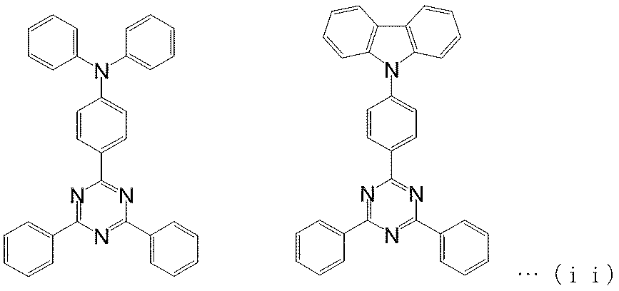

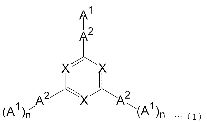
複数個あるA1のうち少なくとも1つは、ヘテロ原子を環構成原子として有していてもよい縮合多環芳香族基を表し、
A2への該縮合多環芳香族基の結合の位置は、

3つのA2は、それぞれ独立に、ヘテロ原子を環構成原子として有していてもよい6員環芳香族基を表し、
A1およびA2において、環構成原子に直接結合している水素原子は、それぞれ独立に、ヘテロ原子を環構成原子として有していてもよい芳香族基、ハロゲン原子、アミノ基、炭素原子数1~12のアルキル基、炭素原子数1~12のアルコキシ基または炭素原子数6~10のアリールオキシ基で置換されていてもよく、
A1およびA2のうち少なくとも1つは、重合性官能基を有する置換基を有し、
3つのXは、それぞれ独立に、1つの水素原子が結合した炭素原子または窒素原子を表し、3つのXのうち少なくとも1つは窒素原子を表し、
2つのnは、それぞれ独立に、1または2を表す。)
[2]上記式(1)で表される単量体が、下記式(1-i)で表されることを特徴とする[1]に記載の高分子化合物。
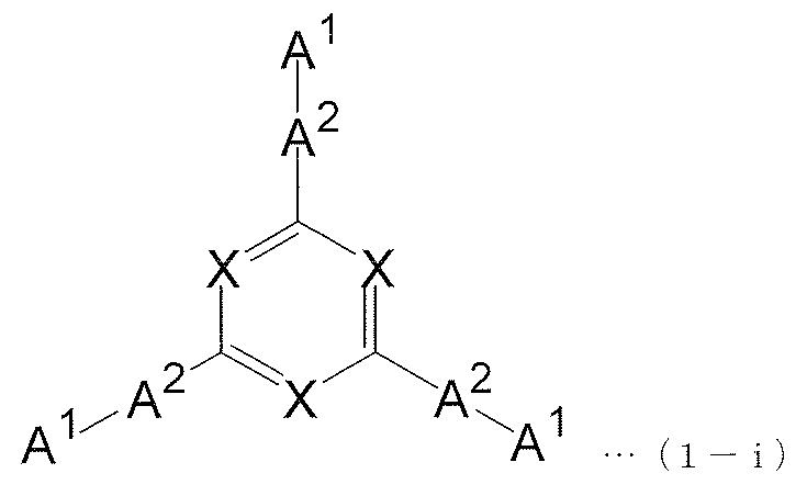
3つのA1のうち少なくとも1つは、ヘテロ原子を環構成原子として有していてもよい縮合多環芳香族基を表し、
A2への該縮合多環芳香族基の結合の位置は、
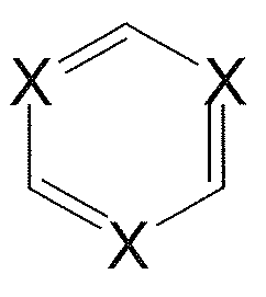
3つのA2は、それぞれ独立に、ヘテロ原子を環構成原子として有していてもよい6員環芳香族基を表し、
A1およびA2において、環構成原子に直接結合している水素原子は、それぞれ独立に、ヘテロ原子を環構成原子として有していてもよい芳香族基、ハロゲン原子、アミノ基、炭素原子数1~12のアルキル基、炭素原子数1~12のアルコキシ基または炭素原子数6~10のアリールオキシ基で置換されていてもよく、
A1およびA2のうち少なくとも1つは、重合性官能基を有する置換基を有し、
3つのXは、それぞれ独立に、1つの水素原子が結合した炭素原子または窒素原子を表し、3つのXのうち少なくとも1つは窒素原子を表す。)
[3]上記式(1-i)において、1つのA1が、重合性官能基を有する置換基を有し、3つのA1のうち少なくとも1つが、重合性官能基を有する置換基を有していてもよいカルバゾリル基あるいはハロゲン原子、アミノ基、炭素原子数1~12のアルキル基、炭素原子数1~12のアルコキシ基、炭素原子数6~10のアリールオキシ基またはヘテロ原子を環構成原子として有していてもよい芳香族基を表すことを特徴とする[2]に記載の高分子化合物。

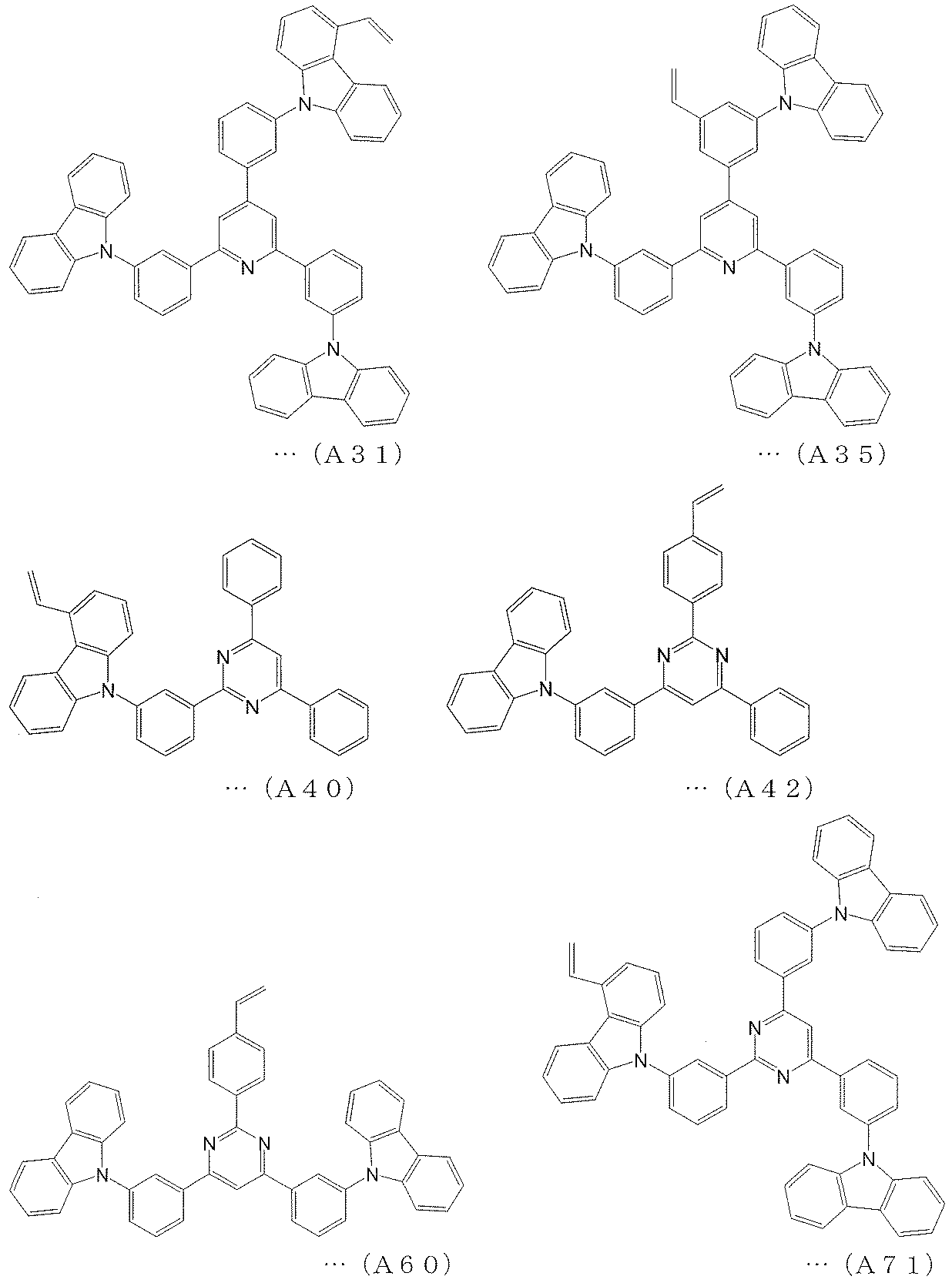


4つのA3は、それぞれ独立に、ヘテロ原子を環構成原子として有していてもよい縮合多環芳香族基を表し、
A2へのA1の結合の位置、およびA4へのA3の結合の位置は、それぞれ
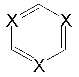
A2および2つのA4は、それぞれ独立に、ヘテロ原子を環構成原子として有していてもよい6員環芳香族基を表し、
A1~A4において、環構成原子に直接結合している水素原子は、それぞれ独立に、ヘテロ原子を環構成原子として有していてもよい芳香族基、ハロゲン原子、アミノ基、炭素原子数1~12のアルキル基、炭素原子数1~12のアルコキシ基または炭素原子数6~10のアリールオキシ基で置換されていてもよく、
A1~A4のうち少なくとも1つは、重合性官能基を有する置換基を有し、
3つのXは、それぞれ独立に、1つの水素原子が結合した炭素原子または窒素原子を表し、3つのXのうち少なくとも1つは窒素原子を表す。)
[6]上記式(1-ii)において、1つのA1が、重合性官能基を有する置換基を有し、4つのA3のうち少なくとも1つが、重合性官能基を有する置換基を有していてもよいカルバゾリル基あるいはハロゲン原子、アミノ基、炭素原子数1~12のアルキル基、炭素原子数1~12のアルコキシ基、炭素原子数6~10のアリールオキシ基またはヘテロ原子を環構成原子として有していてもよい芳香族基を表すことを特徴とする[5]に記載の高分子化合物。
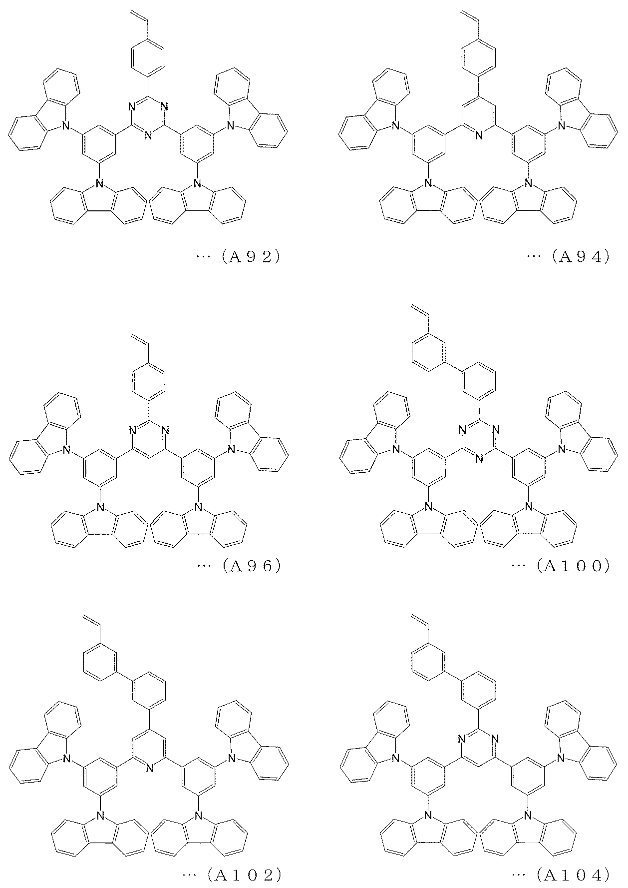
2: 陽極
3: ホール輸送層
4: 発光層
5: 電子輸送層
6: 陰極
本発明の高分子化合物(I)(実施の形態1)は、上記式(1)、好ましくは上記式(1-i)または(1-ii)で表されるキャリア輸送性の重合性化合物から導かれる構成単位を含み、上記式(1)、好ましくは上記式(1-i)または(1-ii)で表されるキャリア輸送性の重合性化合物を重合して得られる。このような高分子化合物(I)を用いると、電子とホールとがともに輸送されるため、駆動電圧が低くなり、耐久性が高い有機EL素子が得られる。
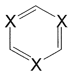

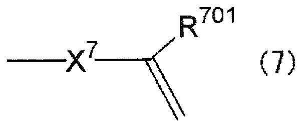


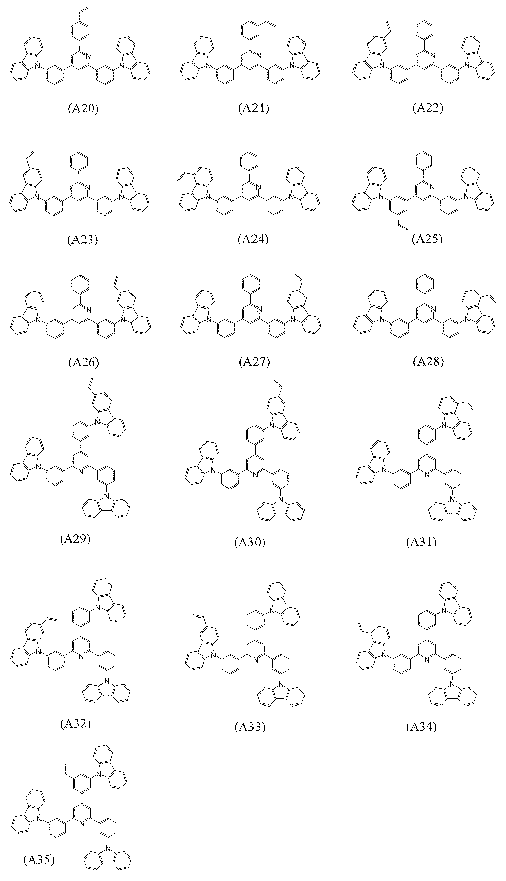

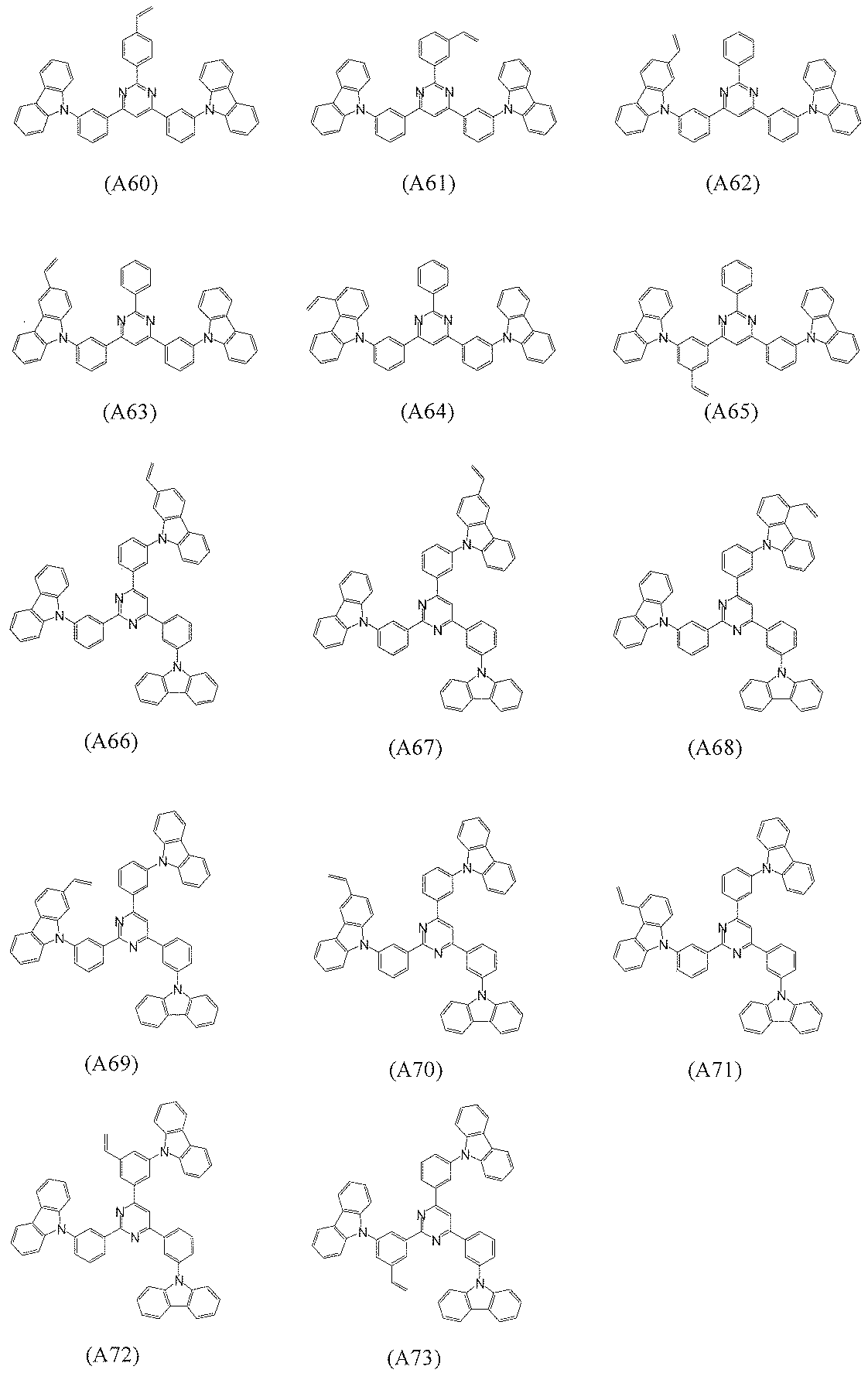

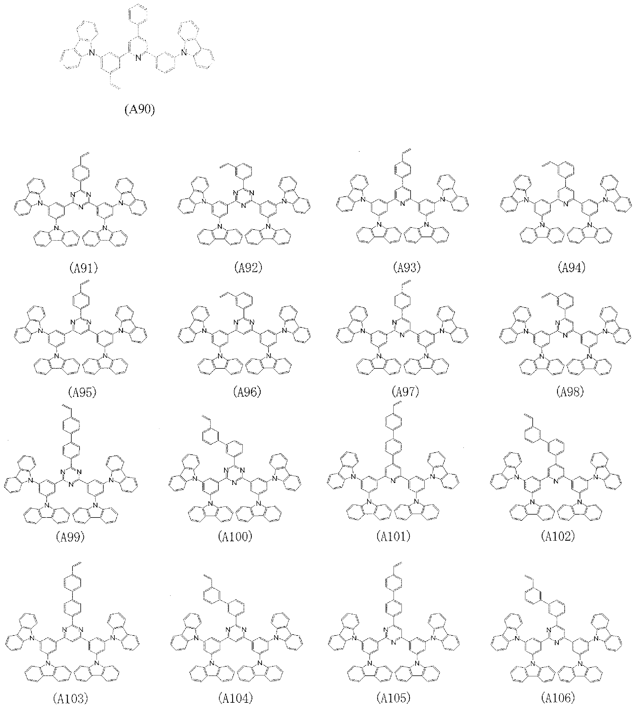
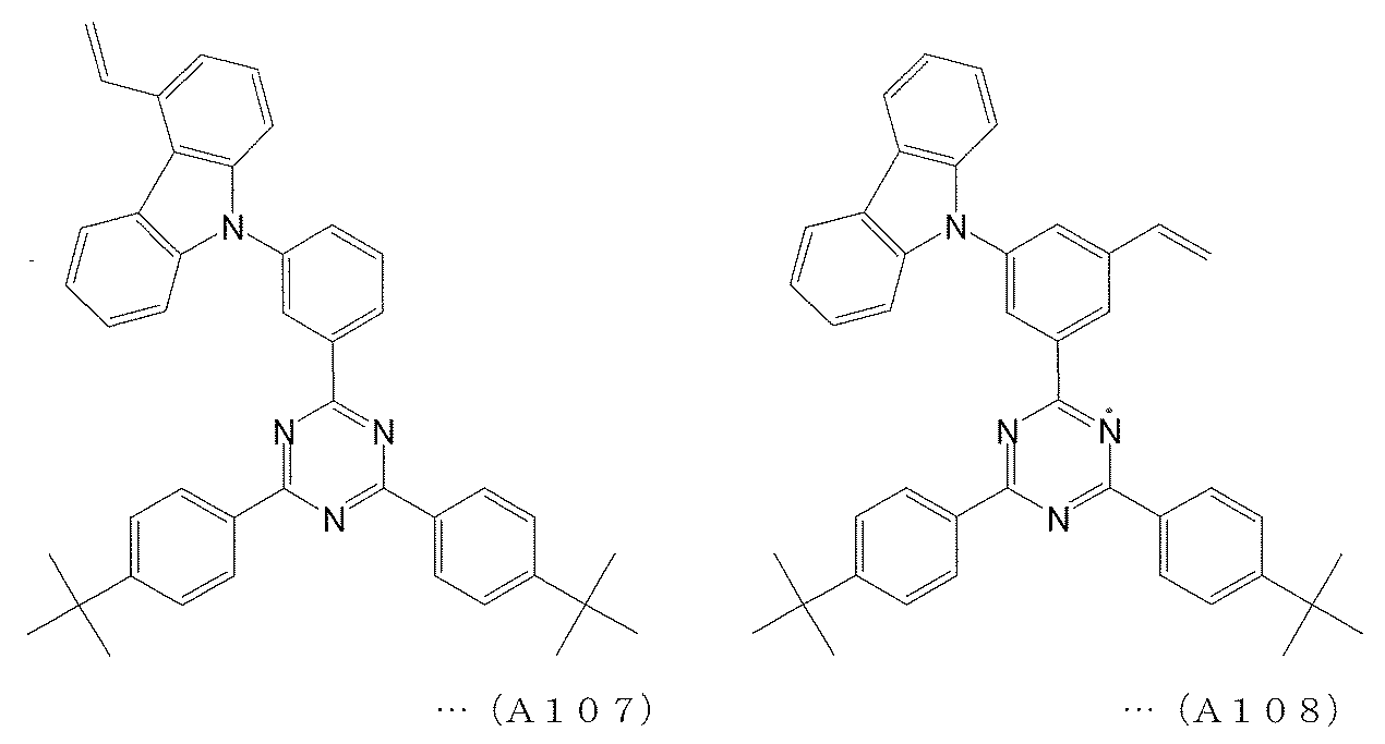
本発明の高分子化合物(II)(実施の形態2)は、上記式(1)で表されるキャリア輸送性の重合性化合物から導かれる構成単位とともに、ホール輸送性の重合性化合物から導かれる単位をさらに含み、上記式(1)で表されるキャリア輸送性の重合性化合物およびホール輸送性の重合性化合物を重合して得られる。


本発明の高分子化合物(III)(実施の形態3)は、上記式(1)で表されるキャリア輸送性の重合性化合物から導かれる構成単位およびホール輸送性の重合性化合物から導かれる構成単位とともに、発光性の重合性化合物から導かれる構成単位をさらに含み、上記式(1)で表されるキャリア輸送性の重合性化合物、ホール輸送性の重合性化合物および発光性の重合性化合物を重合して得られる。

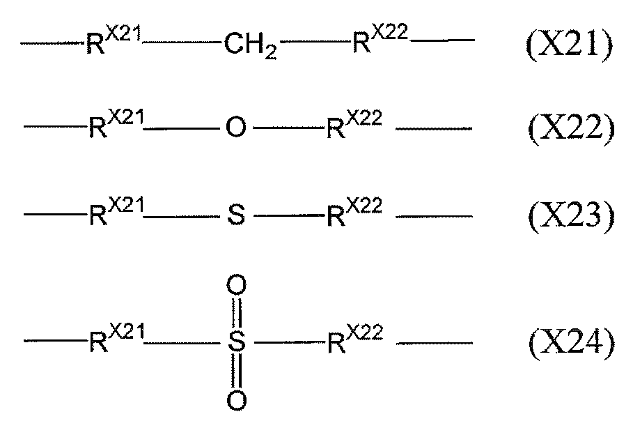


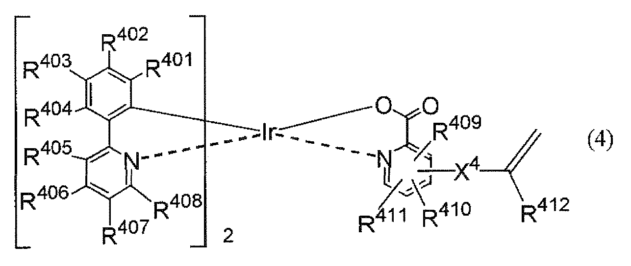
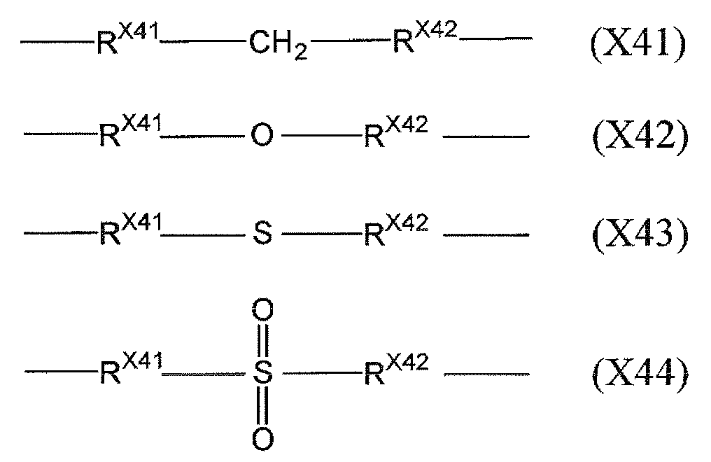
本発明の高分子化合物(IV)(実施の形態4)は、上記式(1)で表されるキャリア輸送性の重合性化合物から導かれる構成単位およびホール輸送性の重合性化合物から導かれる構成単位とともに、電子輸送性の重合性化合物から導かれる構成単位をさらに含み、上記式(1)で表されるキャリア輸送性の重合性化合物、ホール輸送性の重合性化合物および電子輸送性の重合性化合物を重合して得られる。
本発明の高分子化合物(V)(実施の形態5)は、上記式(1)で表されるキャリア輸送性の重合性化合物から導かれる構成単位とホール輸送性の重合性化合物から導かれる構成単位と電子輸送性の重合性化合物から導かれる構成単位と発光性の重合性化合物から導かれる構成単位とを含み、上記式(1)で表されるキャリア輸送性の重合性化合物とホール輸送性の重合性化合物と電子輸送性の重合性化合物と発光性の重合性化合物とを重合して得られる。
本発明の有機EL素子(実施の形態6)では、陽極と陰極との間に、特定の高分子化合物(I)、後述する発光性の化合物および後述するホール輸送性の重合性化合物から導かれる構成単位を有する高分子化合物(I')を含む発光層が一層備えられている。この場合、発光層は、高分子化合物(I)100質量部に対して、上記発光性の化合物を好ましくは0.1~50質量部、より好ましくは0.5~30質量部の量で、高分子化合物(I')を好ましくは10~200質量部、より好ましくは50~150質量部の量で含むことが望ましい。このように、キャリア輸送性の高分子化合物(I)、発光性の化合物およびホール輸送性の高分子化合物(I')から発光層を形成すれば、他の有機材料の層を設けない場合でも、高い発光効率を有する有機EL素子を作製できる。


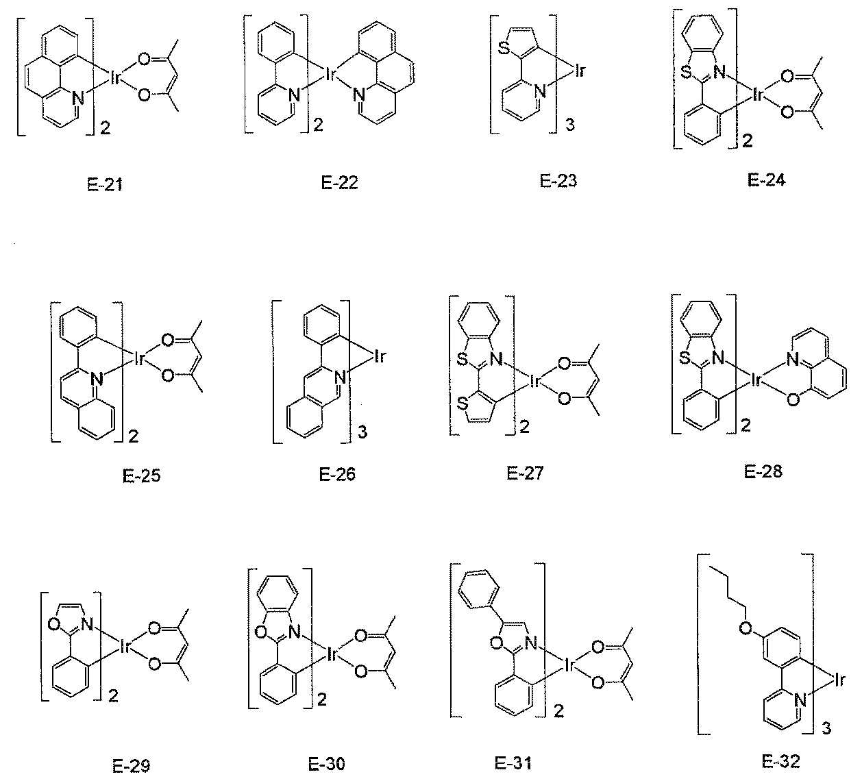
本発明の有機EL素子(実施の形態7)では、陽極と陰極との間に、特定の高分子化合物(II)および実施の形態6に示した発光性の化合物を含む発光層が一層備えられている。この場合、発光層は、高分子化合物(II)100質量部に対して、上記発光性の化合物を好ましくは0.1~50質量部、より好ましくは0.5~30質量部の量で含むことが望ましい。このように、キャリア輸送性およびホール輸送性を併せ持つ高分子化合物(II)および発光性の化合物から発光層を形成すれば、他の有機材料の層を設けない場合でも、高い発光効率を有する有機EL素子を作製できる。
本発明の有機EL素子(実施の形態8)では、陽極と陰極との間に、特定の高分子化合物(III)を含む発光層が一層備えられている。キャリア輸送性、燐光発光性およびホール輸送性を併せ持つ高分子化合物(III)を用いて発光層を形成する場合は、他の有機材料の層を設けない場合でも、高い発光効率を有する有機EL素子を作製できる。さらに、実施の形態8では、高分子化合物(III)のみから発光層を構成できるため、製造工程がより簡略化できる利点もある。
本発明の有機EL素子(実施の形態9)では、陽極と陰極との間に、特定の高分子化合物(IV)および実施の形態6に示した発光性の化合物を含む発光層が一層備えられている。この場合、発光層は、高分子化合物(IV)100質量部に対して、上記発光性の化合物を好ましくは0.1~50質量部、より好ましくは0.5~30質量部の量で含むことが望ましい。このように、キャリア輸送性、電子輸送性およびホール輸送性を併せ持つ高分子化合物(IV)および発光性の化合物から発光層を形成すれば、他の有機材料の層を設けない場合でも、高い発光効率を有する有機EL素子を作製できる。
本発明の有機EL素子(実施の形態10)では、陽極と陰極との間に、特定の高分子化合物(V)を含む発光層が一層備えられている。キャリア輸送性とホール輸送性と電子輸送性と燐光発光性とを併せ持つ高分子化合物(V)を用いて発光層を形成する場合は、他の有機材料の層を設けない場合でも、高い発光効率を有する有機EL素子を作製できる。さらに、実施の形態10では、高分子化合物(V)のみから発光層を構成できるため、製造工程がより簡略化できる利点もある。
本発明に係る有機EL素子は、陽極と陰極との間に、実施の形態6~10で説明した発光層とともに、他の有機層を備えて構成される有機EL素子であってもよい(実施の形態11)。
本発明に係る有機EL素子は、公知の方法で、マトリックス方式またはセグメント方式による画素として画像表示装置に好適である。また、上記有機EL素子は、画素を形成せずに、面発光光源としても好適である。
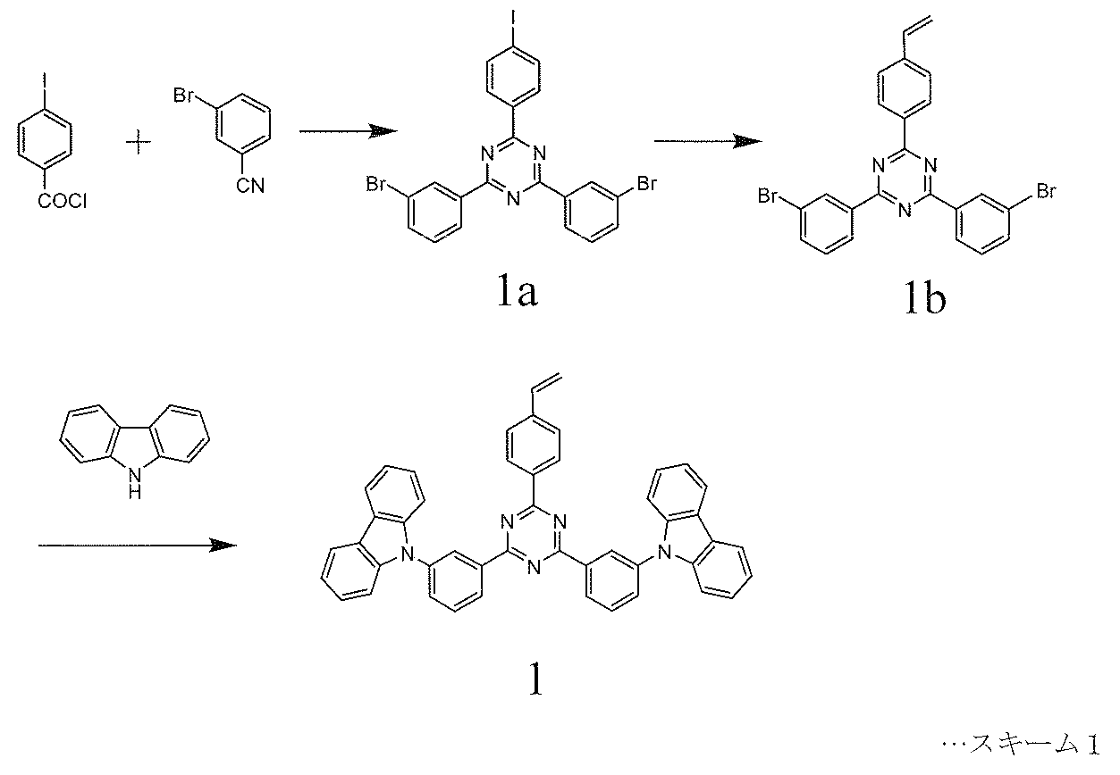
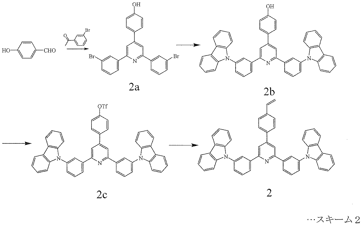


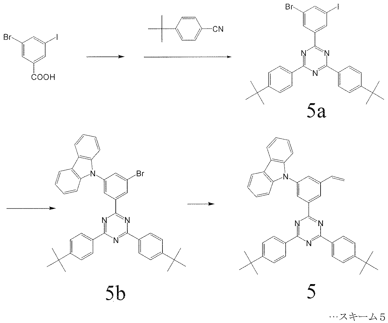
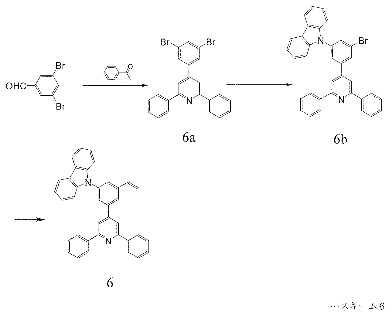


密閉容器に、合成例1で合成したカルバゾリル基導入トリアジンビニルモノマー(1)200mgを入れ、さらに脱水トルエン3.2mLを加えた。次いで、ラジカル重合開始剤であるV-601(和光純薬工業(株)製)のトルエン溶液(0.1M、34μL)を加え、凍結脱気操作を5回繰り返した。真空のまま密閉し、60℃で60時間攪拌した。反応後、反応液をアセトン100mL中に滴下し、沈殿を得た。さらにトルエン-アセトンによる再沈殿操作を2回繰り返した後、50℃で一晩乾燥し、高分子化合物(I-1)を得た。高分子化合物(I-1)の重量平均分子量(Mw)、分子量分布指数(Mw/Mn)を表1に示す。
合成例1で合成した化合物(1)の代わりに、合成例2~6で合成したカルバゾリル基導入トリアジンビニルモノマー(2)、カルバゾリル基導入トリアジンビニルモノマー(3)、カルバゾリル基導入ピリジンビニルモノマー(4)、カルバゾリル基導入トリアジンビニルモノマー(5)およびカルバゾリル基導入ピリジンビニルモノマー(6)をそれぞれ用いた以外は高分子化合物(I-1)と同様にして、高分子化合物(I-2)~(I-6)を得た。得られた高分子化合物の重量平均分子量などを表1に示す。
密閉容器に、合成例1で合成した化合物(1)50mgおよび下記式(8-3)で表されるホール輸送性の重合性化合物を100mg入れ、さらに脱水トルエン2.6mLを加えた。次いでV-601(和光純薬工業(株)製)のトルエン溶液(0.1M、53μL)を加え、凍結脱気操作を5回繰り返した。真空のまま密閉し、60℃で60時間攪拌した。反応後、反応液をアセトン100mL中に滴下し、沈殿を得た。さらにトルエン-アセトンによる再沈殿操作を2回繰り返した後、50℃で一晩乾燥し、高分子化合物(II-1)を得た。高分子化合物(II-1)の重量平均分子量(Mw)、分子量分布指数(Mw/Mn)を表1に示す。ICP元素分析および13C-NMR測定の結果から見積った高分子化合物におけるm/(m+n)の値は、0.64であった。
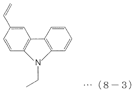
高分子化合物(II-2)~(II-6)の合成は、合成例1で合成した化合物(1)の代わりに、合成例2~6で合成した化合物(2)~(6)をそれぞれ用いた以外は、高分子化合物(II-1)と同様にして高分子化合物(II-2)~(II-6)を得た。得られた高分子化合物の重量平均分子量などを表1に示す。
密閉容器に、合成例1で合成した化合物(1)60mg、ホール輸送性の重合性化合物(8-3)120mgおよび下記式(X)で表される燐光発光性の重合性化合物40mg入れ、さらに脱水トルエン3.1mLを加えた。次いでV-601(和光純薬工業(株)製)のトルエン溶液(0.1M、64μL)を加え、凍結脱気操作を5回繰り返した。真空のまま密閉し、60℃で60時間攪拌した。反応後、反応液をアセトン100mL中に滴下し、沈殿を得た。さらにトルエン-アセトンによる再沈殿操作を2回繰り返した後、50℃で一晩乾燥し、高分子化合物(III-1)を得た。高分子化合物(III-1)の重量平均分子量(Mw)、分子量分布指数(Mw/Mn)を表1に示す。ICP元素分析および13C-NMR測定の結果から見積った高分子化合物におけるm/(m+n)の値は、0.68であり、x/(x+y)の値は、0.16であった。

高分子化合物(III-2)~(III-6)の合成は、合成例1で合成した化合物(1)の代わりに、合成例2~6で合成した化合物(2)~(6)をそれぞれ用いた以外は、高分子化合物(III-1)と同様にして高分子化合物(III-2)~(III-6)を得た。得られた高分子化合物(III-2)~(III-6)の重量平均分子量などは表1に示す。
密閉容器に、合成例1で合成した化合物(1)50mg、ホール輸送性の重合性化合物(8-3)200mgおよび下記式(Y)で表される電子輸送性の重合性化合物を50mg入れ、さらに脱水トルエン5.5mLを加えた。次いでV-601(和光純薬工業(株)製)のトルエン溶液(0.1M、110μL)を加え、凍結脱気操作を5回繰り返した。真空のまま密閉し、60℃で60時間攪拌した。反応後、反応液をアセトン100mL中に滴下し、沈殿を得た。さらにトルエン-アセトンによる再沈殿操作を2回繰り返した後、50℃で一晩乾燥し、高分子化合物(IV-1)を得た。高分子化合物(IV-1)の重量平均分子量(Mw)、分子量分布指数(Mw/Mn)を表1に示す。ICP元素分析および13C-NMR測定の結果から見積った高分子化合物におけるm/(m+n)の値は、0.68であり、x/(x+y)の値は、0.16であった。
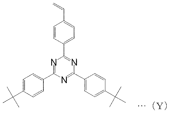
高分子化合物(IV-2)~(IV-6)の合成は、合成例1で合成した化合物(1)の代わりに、合成例2~6で合成した化合物(2)~(6)を用いた以外は、高分子化合物(IV-1)と同様にして高分子化合物(IV-2)~(IV-6)を得た。得られた高分子化合物(IV-2)~(IV-6)の重量平均分子量などは表1に示す。

まず、高分子化合物(I')を以下のようにして合成した。密閉容器に、ホール輸送性の重合性化合物(8-3)200mgを入れ、さらに脱水トルエン4.5mLを加えた。次いでV-601(和光純薬工業(株)製)のトルエン溶液(0.1M、90μL)を加え、凍結脱気操作を5回繰り返した。真空のまま密閉し、60℃で60時間攪拌した。反応後、反応液をアセトン100mL中に滴下し、沈殿を得た。さらにトルエン-アセトンによる再沈殿操作を2回繰り返した後、50℃で一晩乾燥し、高分子化合物(I')を得た。
高分子化合物(I-1)の代わりに高分子化合物(I-2)~(I-6)を用いた以外は、実施例25と同様の方法によって有機EL素子2~6を作製し、その発光輝度を測定した。有機EL素子2~6の最大外部量子効率、最高到達輝度、駆動電圧、初期輝度100cd/m2で点灯させて定電流駆動した時の輝度半減寿命を表2に示す。
高分子化合物(I-1)および高分子化合物(I')の代わりに、それぞれ高分子化合物(II-1)~(II-6)を用いた以外は、実施例25と同様にしてそれぞれ有機EL素子7~12を作製し、その発光輝度を測定した。有機EL素子7~12の最大外部量子効率、最高到達輝度、駆動電圧、初期輝度100cd/m2で点灯させて定電流駆動した時の輝度半減寿命を表2に示す。
高分子化合物(II-1)と発光性の化合物(E-38)の代わりに、それぞれ高分子化合物(III-1)~(III-6)を用いた以外は、実施例31と同様にしてそれぞれ有機EL素子13~18を作製し、その発光輝度を測定した。有機EL素子13~18の最大外部量子効率、最高到達輝度、駆動電圧、初期輝度100cd/m2で点灯させて定電流駆動した時の輝度半減寿命を表2に示す。
高分子化合物(III-1)の代わりに、それぞれ高分子化合物(IV-1)~(IV-6)を用いた以外は、実施例37と同様にしてそれぞれ有機EL素子19~24を作製し、その発光輝度を測定した。有機EL素子19~24の最大外部量子効率、最高到達輝度、駆動電圧、初期輝度100cd/m2で点灯させて定電流駆動した時の輝度半減寿命を表2に示す。
高分子化合物(I-1)の代わりに低分子化合物7を用いた以外は、実施例25と同様にして有機EL素子25を作製し、その発光輝度を測定した。有機EL素子25の最大外部量子効率、最高到達輝度、駆動電圧、初期輝度100cd/m2で点灯させて定電流駆動した時の輝度半減寿命を表2に示す。
高分子化合物(I-1)の代わりに低分子化合物8を用いた以外は、実施例25と同様にして有機EL素子26を作製し、その発光輝度を測定した。有機EL素子26の最大外部量子効率、最高到達輝度、駆動電圧、初期輝度100cd/m2で点灯させて定電流駆動した時の輝度半減寿命を表2に示す。
まず、合成例1で合成した化合物(1)の代わりに、合成例9で合成したカルバゾリル基導入トリアジンビニルモノマー(9)を用いた以外は高分子化合物(I-1)と同様にて、高分子化合物(I'')を得た。得られた高分子化合物(I'')の重量平均分子量は、68,000、分子量分布指数は2.14であった。
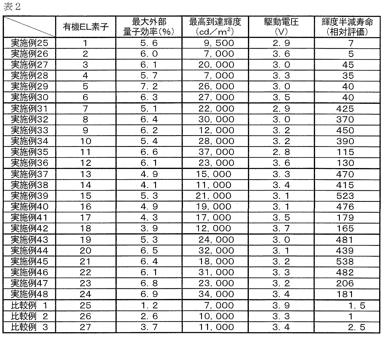
Claims (20)
- 下記式(1)で表される単量体から導かれる構成単位を含むことを特徴とする高分子化合物。

複数個あるA1のうち少なくとも1つは、ヘテロ原子を環構成原子として有していてもよい縮合多環芳香族基を表し、
A2への該縮合多環芳香族基の結合の位置は、
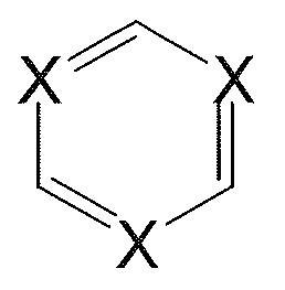
3つのA2は、それぞれ独立に、ヘテロ原子を環構成原子として有していてもよい6員環芳香族基を表し、
A1およびA2において、環構成原子に直接結合している水素原子は、それぞれ独立に、ヘテロ原子を環構成原子として有していてもよい芳香族基、ハロゲン原子、アミノ基、炭素原子数1~12のアルキル基、炭素原子数1~12のアルコキシ基または炭素原子数6~10のアリールオキシ基で置換されていてもよく、
A1およびA2のうち少なくとも1つは、重合性官能基を有する置換基を有し、
3つのXは、それぞれ独立に、1つの水素原子が結合した炭素原子または窒素原子を表し、3つのXのうち少なくとも1つは窒素原子を表し、
2つのnは、それぞれ独立に、1または2を表す。) - 上記式(1)で表される単量体が、下記式(1-i)で表される単量体であることを特徴とする請求項1に記載の高分子化合物。

3つのA1のうち少なくとも1つは、ヘテロ原子を環構成原子として有していてもよい縮合多環芳香族基を表し、
A2への該縮合多環芳香族基の結合の位置は、
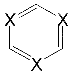
3つのA2は、それぞれ独立に、ヘテロ原子を環構成原子として有していてもよい6員環芳香族基を表し、
A1およびA2において、環構成原子に直接結合している水素原子は、それぞれ独立に、ヘテロ原子を環構成原子として有していてもよい芳香族基、ハロゲン原子、アミノ基、炭素原子数1~12のアルキル基、炭素原子数1~12のアルコキシ基または炭素原子数6~10のアリールオキシ基で置換されていてもよく、
A1およびA2のうち少なくとも1つは、重合性官能基を有する置換基を有し、
3つのXは、それぞれ独立に、1つの水素原子が結合した炭素原子または窒素原子を表し、3つのXのうち少なくとも1つは窒素原子を表す。) - 上記式(1-i)において、1つのA1が、重合性官能基を有する置換基を有し、
3つのA1のうち少なくとも1つが、重合性官能基を有する置換基を有していてもよいカルバゾリル基あるいはハロゲン原子、アミノ基、炭素原子数1~12のアルキル基、炭素原子数1~12のアルコキシ基、炭素原子数6~10のアリールオキシ基またはヘテロ原子を環構成原子として有していてもよい芳香族基を表すことを特徴とする請求項2に記載の高分子化合物。 - 上記式(1-i)で表される単量体が、下記式(A1)、(A13)、(A14)、(A15)、(A31)、(A35)、(A40)、(A42)、(A60)、(A71)、(A73)、(A78)、(A79)、(A80)、(A88)、(A89)、(A107)または(A108)で表される単量体であることを特徴とする請求項2または3に記載の高分子化合物。
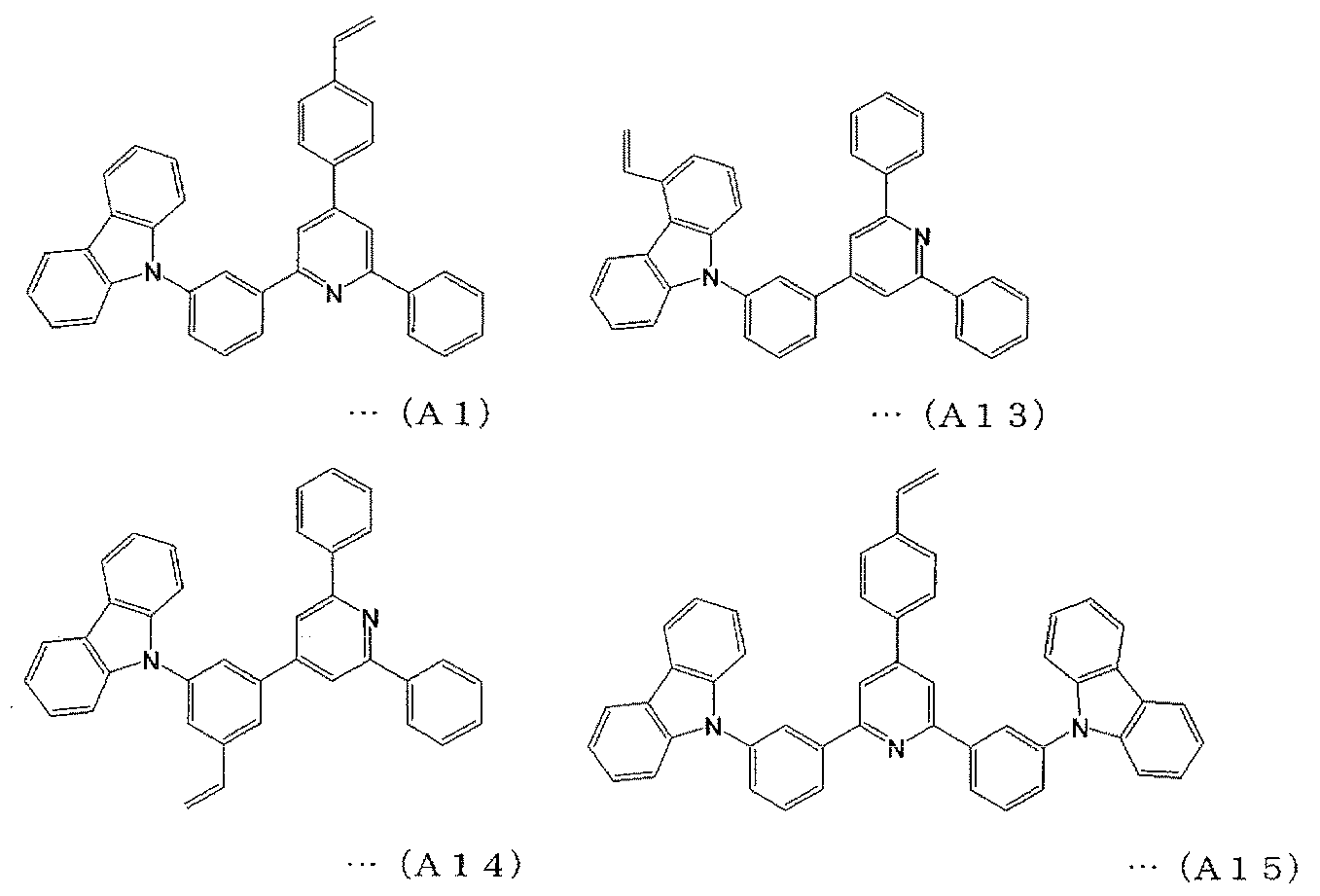
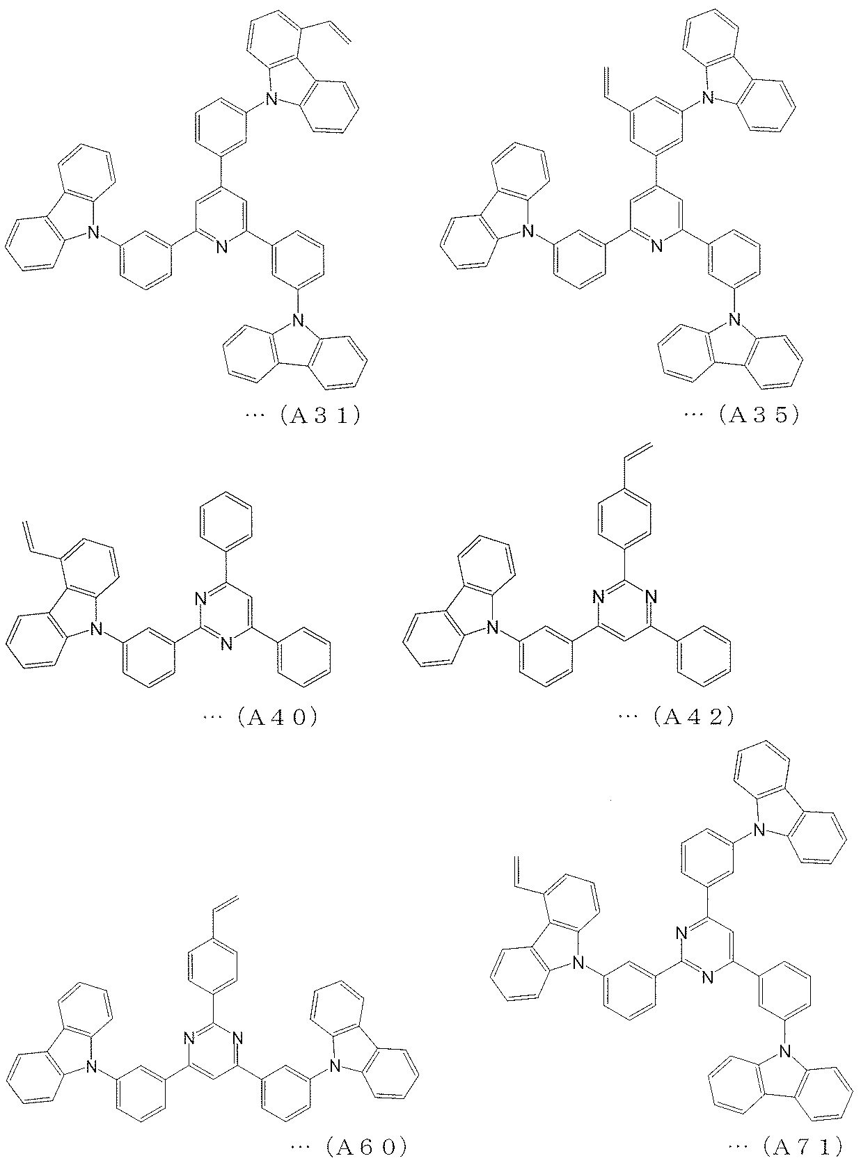
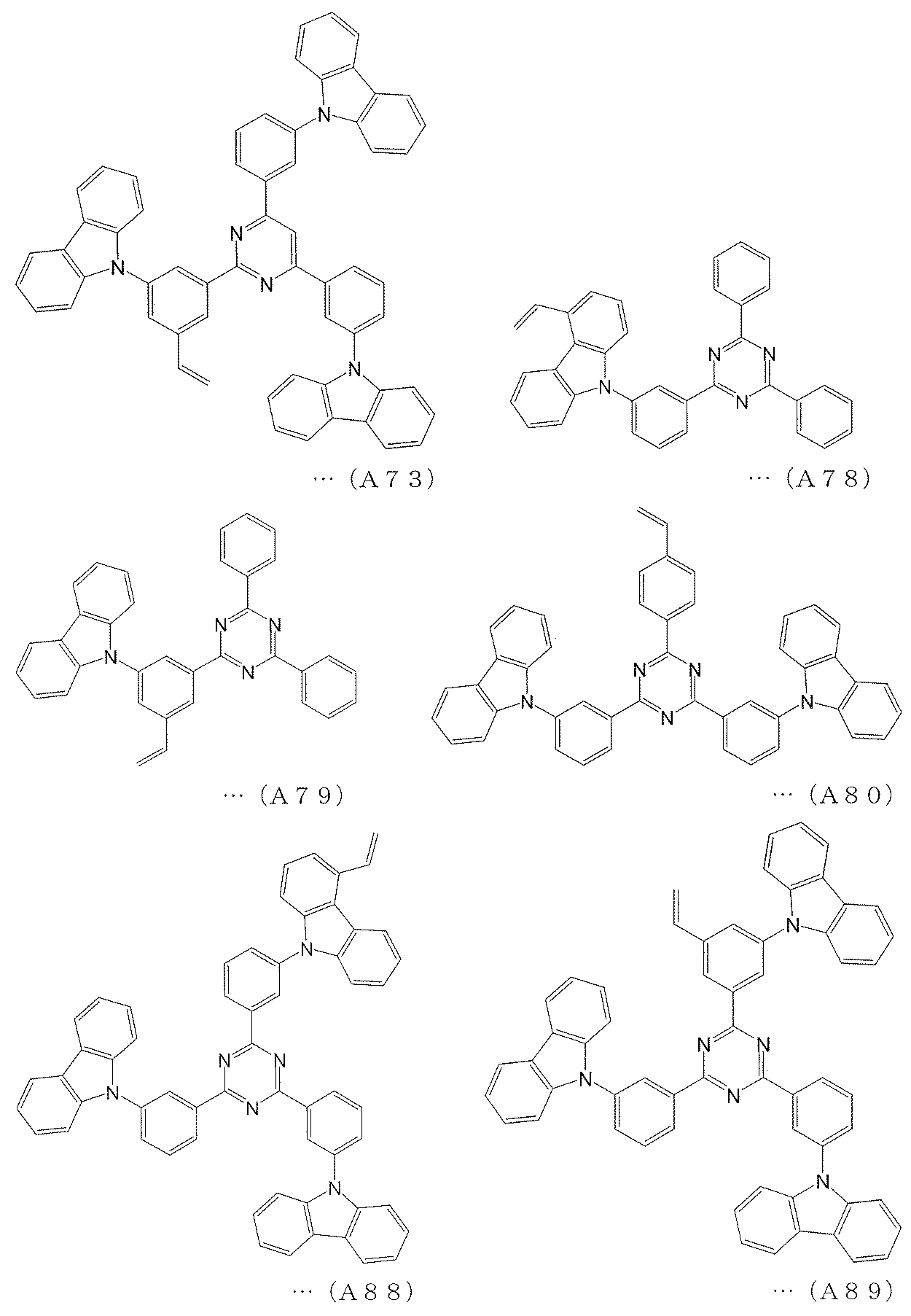

- 上記式(1)で表される単量体が、下記式(1-ii)で表されることを特徴とする請求項1に記載の高分子化合物。
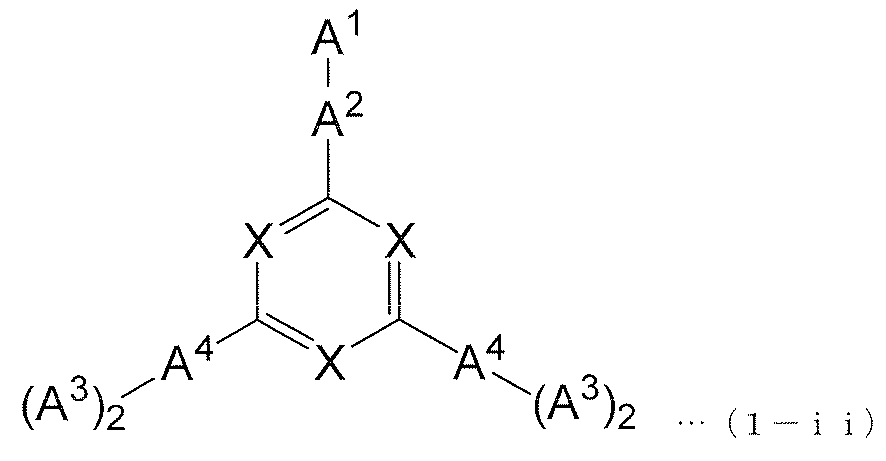
4つのA3は、それぞれ独立に、ヘテロ原子を環構成原子として有していてもよい縮合多環芳香族基を表し、
A2へのA1の結合の位置、およびA4へのA3の結合の位置は、それぞれ

A2および2つのA4は、それぞれ独立に、ヘテロ原子を環構成原子として有していてもよい6員環芳香族基を表し、
A1~A4において、環構成原子に直接結合している水素原子は、それぞれ独立に、ヘテロ原子を環構成原子として有していてもよい芳香族基、ハロゲン原子、アミノ基、炭素原子数1~12のアルキル基、炭素原子数1~12のアルコキシ基または炭素原子数6~10のアリールオキシ基で置換されていてもよく、
A1~A4のうち少なくとも1つは、重合性官能基を有する置換基を有し、
3つのXは、それぞれ独立に、1つの水素原子が結合した炭素原子または窒素原子を表し、3つのXのうち少なくとも1つは窒素原子を表す。) - 上記式(1-ii)において、A1が、重合性官能基を有する置換基を表し、4つのA3のうち少なくとも1つが、重合性官能基を有する置換基を有していてもよいカルバゾリル基あるいはハロゲン原子、アミノ基、炭素原子数1~12のアルキル基、炭素原子数1~12のアルコキシ基、炭素原子数6~10のアリールオキシ基またはヘテロ原子を環構成原子として有していてもよい芳香族基を表すことを特徴とする請求項5に記載の高分子化合物。
- 上記式(1-ii)で表される単量体が、下記式(A92)、(A94)、(A96)、(A100)、(A102)または(A104)で表されることを特徴とする請求項5または6に記載の高分子化合物。
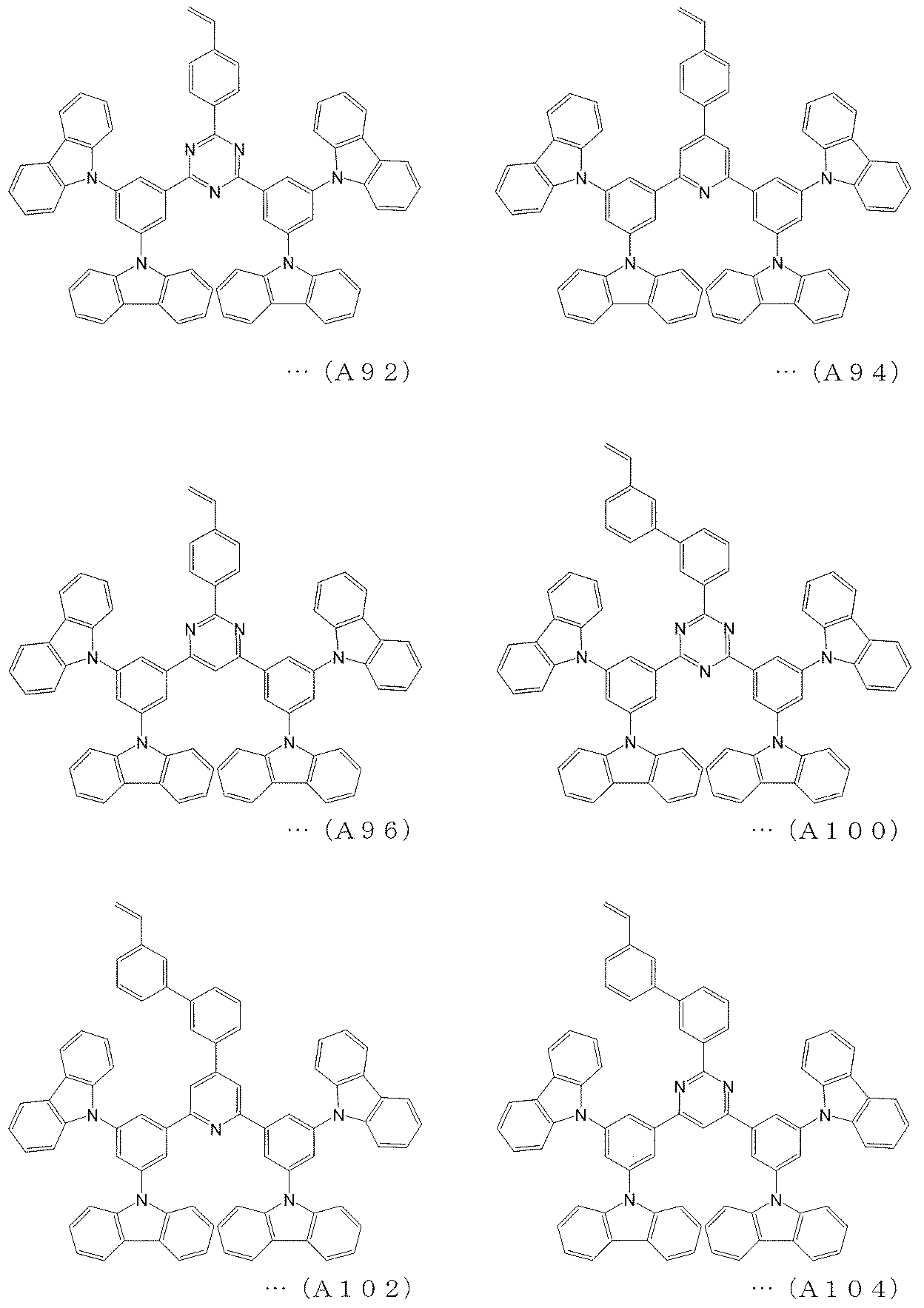
- ホール輸送性の重合性化合物から導かれる構成単位をさらに含むことを特徴とする請求項1~7のいずれかに記載の高分子化合物。
- 上記ホール輸送性の重合性化合物が、カルバゾール構造またはトリフェニルアミン構造を含むことを特徴とする請求項8に記載の高分子化合物。
- 上記ホール輸送性の重合性化合物が、カルバゾール構造を含むことを特徴とする請求項9に記載の高分子化合物。
- 電子輸送性の重合性化合物から導かれる構成単位および発光性の重合性化合物から導かれる構成単位のうち少なくとも1つをさらに含むことを特徴とする請求項1~10のいずれかに記載の高分子化合物。
- 上記発光性の重合性化合物が、燐光発光性を有することを特徴とする請求項11に記載の高分子化合物。
- 上記発光性の重合性化合物が、遷移金属錯体であることを特徴とする請求項11または12に記載の高分子化合物。
- 上記遷移金属錯体が、イリジウム錯体であることを特徴とする請求項13に記載の高分子化合物。
- 上記電子輸送性の重合性化合物が、芳香族複素環置換基またはトリアリールホウ素置換基を有することを特徴とする請求項11~14のいずれかに記載の高分子化合物。
- 有機エレクトロルミネッセンス素子に用いられることを特徴とする請求項1~15のいずれかに記載の高分子化合物。
- 請求項1~16のいずれかに記載の高分子化合物を含むことを特徴とする有機エレクトロルミネッセンス素子用発光層。
- 陽極と陰極との間に1層以上の有機層を含む有機エレクトロルミネッセンス素子であって、該有機層が含む発光層の少なくとも1層が、請求項1~16のいずれかに記載の高分子化合物を含むことを特徴とする有機エレクトロルミネッセンス素子。
- 請求項18に記載の有機エレクトロルミネッセンス素子を備えることを特徴とする、ディスプレイ、バックライト、電子写真、照明光源、記録光源、露光光源、読み取り光源、標識、看板、インテリアおよび光通信システムからなる群から選択される物品。
- 請求項17に記載の発光層が少なくとも1層含まれる有機層を陽極上に形成する工程、および
該有機層上に陰極を形成する工程
を含むことを特徴とする有機エレクトロルミネッセンス素子の製造方法。
Priority Applications (5)
| Application Number | Priority Date | Filing Date | Title |
|---|---|---|---|
| CN200980105946.1A CN102317328B (zh) | 2008-02-22 | 2009-02-20 | 高分子化合物和使用该高分子化合物的有机电致发光元件 |
| EP09713629.5A EP2246370B1 (en) | 2008-02-22 | 2009-02-20 | Polymer compound and organic electroluminescent device using the same |
| JP2009554382A JP5314602B2 (ja) | 2008-02-22 | 2009-02-20 | 高分子化合物およびこれを用いた有機エレクトロルミネッセンス素子 |
| KR1020107021123A KR101171556B1 (ko) | 2008-02-22 | 2009-02-20 | 고분자 화합물 및 이것을 사용한 유기 전계 발광 소자 |
| US12/918,742 US8617722B2 (en) | 2008-02-22 | 2009-02-20 | Polymer compound and organic electroluminescence element using the same |
Applications Claiming Priority (2)
| Application Number | Priority Date | Filing Date | Title |
|---|---|---|---|
| JP2008041902 | 2008-02-22 | ||
| JP2008-041902 | 2008-02-22 |
Publications (1)
| Publication Number | Publication Date |
|---|---|
| WO2009104708A1 true WO2009104708A1 (ja) | 2009-08-27 |
Family
ID=40985585
Family Applications (1)
| Application Number | Title | Priority Date | Filing Date |
|---|---|---|---|
| PCT/JP2009/052955 WO2009104708A1 (ja) | 2008-02-22 | 2009-02-20 | 高分子化合物およびこれを用いた有機エレクトロルミネッセンス素子 |
Country Status (7)
| Country | Link |
|---|---|
| US (1) | US8617722B2 (ja) |
| EP (1) | EP2246370B1 (ja) |
| JP (1) | JP5314602B2 (ja) |
| KR (1) | KR101171556B1 (ja) |
| CN (1) | CN102317328B (ja) |
| TW (1) | TWI438210B (ja) |
| WO (1) | WO2009104708A1 (ja) |
Cited By (20)
| Publication number | Priority date | Publication date | Assignee | Title |
|---|---|---|---|---|
| JP2010095452A (ja) * | 2008-10-14 | 2010-04-30 | Tosoh Corp | 1,3,5−トリアジン化合物及びその製造方法 |
| WO2010080471A1 (en) * | 2009-01-08 | 2010-07-15 | General Electric Company | 2,4,6-tri-(heteroarylphenyl)-pyridines and electron-transporting materials comprising them |
| WO2011027749A1 (ja) * | 2009-09-01 | 2011-03-10 | 富士フイルム株式会社 | 有機電界発光素子、有機電界発光素子の製造方法、表示装置及び照明装置 |
| US7989476B2 (en) | 2009-01-08 | 2011-08-02 | General Electric Company | Electron-transporting materials and processes for making the same |
| JP2012501091A (ja) * | 2008-08-25 | 2012-01-12 | チェイル インダストリーズ インコーポレイテッド | 有機光電素子用材料およびこれを含む有機光電素子 |
| JP2012062450A (ja) * | 2010-09-17 | 2012-03-29 | Idemitsu Kosan Co Ltd | 新規重合性単量体と高分子化合物、それを用いた有機デバイス用材料、有機エレクトロルミネッセンス用材料、有機デバイス及び有機エレクトロルミネッセンス素子 |
| JP2012079893A (ja) * | 2010-09-30 | 2012-04-19 | Fujifilm Corp | 組成物、並びに、該組成物を用いた膜、電荷輸送層、有機電界発光素子、及び電荷輸送層の形成方法 |
| WO2012086170A1 (ja) * | 2010-12-20 | 2012-06-28 | 出光興産株式会社 | 芳香族複素環誘導体及びそれを用いた有機エレクトロルミネッセンス素子 |
| JP2012149257A (ja) * | 2011-01-17 | 2012-08-09 | Samsung Electronics Co Ltd | 高分子及び該高分子を含んだ有機発光素子 |
| US20130264560A1 (en) * | 2010-12-20 | 2013-10-10 | E I Du Pont De Nemours And Company | Triazine derivatives for electronic applications |
| JP2013538883A (ja) * | 2010-07-16 | 2013-10-17 | メルク パテント ゲーエムベーハー | 有機エレクトロルミネッセンス素子のためのポリマー材料 |
| JP2014056829A (ja) * | 2008-05-16 | 2014-03-27 | Semiconductor Energy Lab Co Ltd | 発光装置および電子機器 |
| JP2014148663A (ja) * | 2012-12-21 | 2014-08-21 | Cambridge Display Technology Ltd | ポリマーおよび有機発光デバイス |
| JP2015160844A (ja) * | 2014-02-28 | 2015-09-07 | 三星ディスプレイ株式會社Samsung Display Co.,Ltd. | トリアジン(triazine)誘導体及びこれを用いた有機発光素子 |
| US9196835B2 (en) | 2010-12-13 | 2015-11-24 | Samsung Electronics Co., Ltd. | Polymer, method of manufacture thereof, and organic light-emitting device including the polymer |
| JP2016141633A (ja) * | 2015-01-30 | 2016-08-08 | 東ソー株式会社 | トリアジン化合物、その製造方法、及びそれを用いた有機電界発光素子 |
| JPWO2014057852A1 (ja) * | 2012-10-09 | 2016-09-05 | 出光興産株式会社 | 共重合体、有機電子素子用材料、有機エレクトロルミネッセンス素子用材料及び有機エレクトロルミネッセンス素子 |
| JP2017069385A (ja) * | 2015-09-30 | 2017-04-06 | 日立化成株式会社 | 電荷輸送性材料、該材料を用いたインク組成物、有機エレクトロニクス素子、有機エレクトロルミネセンス素子、表示素子、照明装置、及び表示装置 |
| JP2017123362A (ja) * | 2016-01-04 | 2017-07-13 | 日立化成株式会社 | 有機エレクトロニクス材料及びその利用 |
| WO2021125011A1 (ja) * | 2019-12-16 | 2021-06-24 | 三菱ケミカル株式会社 | 重合体、有機電界発光素子用組成物、正孔輸送層又は正孔注入層形成用組成物、有機電界発光素子、有機el表示装置及び有機el照明 |
Families Citing this family (15)
| Publication number | Priority date | Publication date | Assignee | Title |
|---|---|---|---|---|
| JP5342442B2 (ja) * | 2007-07-13 | 2013-11-13 | 昭和電工株式会社 | トリアジン環含有高分子化合物および該高分子化合物を用いた有機発光素子 |
| CN101689613B (zh) * | 2007-07-13 | 2011-12-14 | 昭和电工株式会社 | 使用含三嗪环的高分子化合物而成的有机发光元件 |
| US20110042664A1 (en) * | 2008-04-24 | 2011-02-24 | Showa Denko K.K. | Charge-transporting polymer compound and organic electroluminescence element using the same |
| TW201231459A (en) * | 2010-12-20 | 2012-08-01 | Du Pont | Electroactive compositions for electronic applications |
| KR20130032675A (ko) * | 2011-09-23 | 2013-04-02 | 삼성디스플레이 주식회사 | 듀얼 모드 유기발광소자 및 이를 포함하는 화소 회로 |
| KR102261235B1 (ko) | 2011-11-22 | 2021-06-04 | 이데미쓰 고산 가부시키가이샤 | 방향족 복소 고리 유도체, 유기 일렉트로루미네선스 소자용 재료 및 유기 일렉트로루미네선스 소자 |
| WO2013096921A1 (en) * | 2011-12-22 | 2013-06-27 | Georgia Tech Research Corporation | Non-crosslinked polystyrene triscarbazole hole transport materials |
| WO2013096918A1 (en) * | 2011-12-22 | 2013-06-27 | Georgia Tech Research Corporation | Crosslinking triscarbazole hole transport polymers |
| CN103304487A (zh) * | 2012-03-15 | 2013-09-18 | 海洋王照明科技股份有限公司 | 含嘧啶的有机半导体材料及其制备方法和有机电致发光器件 |
| CN104017563A (zh) * | 2013-02-28 | 2014-09-03 | 海洋王照明科技股份有限公司 | 双极性蓝光磷光材料及其制备方法和有机电致发光器件 |
| KR101882592B1 (ko) | 2013-11-13 | 2018-08-24 | 이데미쓰 고산 가부시키가이샤 | 화합물, 유기 일렉트로루미네선스 소자용 재료, 유기 일렉트로루미네선스 소자 및 전자 기기 |
| CN104370887B (zh) * | 2013-12-26 | 2016-08-24 | 北京阿格蕾雅科技发展有限公司 | 2,6-双[3-(n-咔唑基)苯基]吡啶类化合物的合成方法 |
| US10784446B2 (en) | 2014-11-28 | 2020-09-22 | Idemitsu Kosan Co., Ltd. | Compound, organic electroluminescence element material, organic electroluminescence element and electronic device |
| US20200095226A1 (en) * | 2016-12-08 | 2020-03-26 | Guangzhou Chinaray Optoelectronic Materials Ltd. | Triazine fused ring derivative and application thereof in organic electronic device |
| KR102153086B1 (ko) * | 2018-07-31 | 2020-09-07 | 주식회사 엘지화학 | 신규한 고분자 및 이를 포함하는 유기 발광 소자 |
Citations (10)
| Publication number | Priority date | Publication date | Assignee | Title |
|---|---|---|---|---|
| JP2002129155A (ja) | 2000-10-30 | 2002-05-09 | Toyo Ink Mfg Co Ltd | 蛍光発光材料 |
| JP2003022893A (ja) | 2001-07-06 | 2003-01-24 | Fuji Photo Film Co Ltd | 発光素子 |
| WO2003080760A1 (fr) | 2002-03-22 | 2003-10-02 | Idemitsu Kosan Co., Ltd. | Materiau pour dispositifs electroluminescents organiques et dispositifs electroluminescents organiques produits avec ce materiau |
| JP2006173569A (ja) | 2004-12-15 | 2006-06-29 | Korea Electronics Telecommun | トリアジン誘導体化合物を含む有機電界発光素子 |
| JP2006188493A (ja) | 2004-12-10 | 2006-07-20 | Pioneer Electronic Corp | 有機化合物、電荷輸送材料および有機電界発光素子 |
| JP2006225428A (ja) * | 2005-02-15 | 2006-08-31 | Tokyo Institute Of Technology | 1,3,5−トリアジン環を有する共重合体、その製造法およびその使用 |
| JP2007153917A (ja) * | 2005-11-30 | 2007-06-21 | Showa Denko Kk | 高分子発光材料、有機エレクトロルミネッセンス素子および表示装置 |
| JP2007169541A (ja) * | 2005-12-26 | 2007-07-05 | Konica Minolta Holdings Inc | 有機エレクトロルミネッセンス素子用材料、有機エレクトロルミネッセンス素子、表示装置及び照明装置 |
| JP2007269895A (ja) * | 2006-03-30 | 2007-10-18 | Showa Denko Kk | 高分子発光材料、有機エレクトロルミネッセンス素子および表示装置 |
| JP2008028119A (ja) * | 2006-07-20 | 2008-02-07 | Showa Denko Kk | 有機エレクトロルミネッセンス素子およびその用途 |
Family Cites Families (8)
| Publication number | Priority date | Publication date | Assignee | Title |
|---|---|---|---|---|
| JP3482719B2 (ja) | 1994-12-07 | 2004-01-06 | 凸版印刷株式会社 | キャリア輸送性重合体 |
| JPH101665A (ja) | 1996-06-18 | 1998-01-06 | Toyota Central Res & Dev Lab Inc | 電界発光素子 |
| JP4344494B2 (ja) * | 2000-08-24 | 2009-10-14 | 富士フイルム株式会社 | 発光素子及び新規重合体子 |
| KR100543837B1 (ko) * | 2001-09-04 | 2006-01-23 | 캐논 가부시끼가이샤 | 고분자 화합물 및 유기 발광 소자 |
| US6730417B2 (en) * | 2002-01-29 | 2004-05-04 | Xerox Corporation | Organic electroluminescent (EL) devices |
| JP4225043B2 (ja) | 2002-12-03 | 2009-02-18 | コニカミノルタホールディングス株式会社 | 有機エレクトロルミネッセンス素子、その製造方法、表示装置、照明装置及び光源 |
| JP2007227888A (ja) * | 2005-12-16 | 2007-09-06 | Fujifilm Corp | 有機電界発光素子 |
| US7943245B2 (en) * | 2005-12-16 | 2011-05-17 | Fujifilm Corporation | Organic electroluminescent device |
-
2009
- 2009-02-20 JP JP2009554382A patent/JP5314602B2/ja active Active
- 2009-02-20 EP EP09713629.5A patent/EP2246370B1/en active Active
- 2009-02-20 CN CN200980105946.1A patent/CN102317328B/zh active Active
- 2009-02-20 US US12/918,742 patent/US8617722B2/en active Active
- 2009-02-20 WO PCT/JP2009/052955 patent/WO2009104708A1/ja active Application Filing
- 2009-02-20 TW TW098105487A patent/TWI438210B/zh active
- 2009-02-20 KR KR1020107021123A patent/KR101171556B1/ko active IP Right Grant
Patent Citations (10)
| Publication number | Priority date | Publication date | Assignee | Title |
|---|---|---|---|---|
| JP2002129155A (ja) | 2000-10-30 | 2002-05-09 | Toyo Ink Mfg Co Ltd | 蛍光発光材料 |
| JP2003022893A (ja) | 2001-07-06 | 2003-01-24 | Fuji Photo Film Co Ltd | 発光素子 |
| WO2003080760A1 (fr) | 2002-03-22 | 2003-10-02 | Idemitsu Kosan Co., Ltd. | Materiau pour dispositifs electroluminescents organiques et dispositifs electroluminescents organiques produits avec ce materiau |
| JP2006188493A (ja) | 2004-12-10 | 2006-07-20 | Pioneer Electronic Corp | 有機化合物、電荷輸送材料および有機電界発光素子 |
| JP2006173569A (ja) | 2004-12-15 | 2006-06-29 | Korea Electronics Telecommun | トリアジン誘導体化合物を含む有機電界発光素子 |
| JP2006225428A (ja) * | 2005-02-15 | 2006-08-31 | Tokyo Institute Of Technology | 1,3,5−トリアジン環を有する共重合体、その製造法およびその使用 |
| JP2007153917A (ja) * | 2005-11-30 | 2007-06-21 | Showa Denko Kk | 高分子発光材料、有機エレクトロルミネッセンス素子および表示装置 |
| JP2007169541A (ja) * | 2005-12-26 | 2007-07-05 | Konica Minolta Holdings Inc | 有機エレクトロルミネッセンス素子用材料、有機エレクトロルミネッセンス素子、表示装置及び照明装置 |
| JP2007269895A (ja) * | 2006-03-30 | 2007-10-18 | Showa Denko Kk | 高分子発光材料、有機エレクトロルミネッセンス素子および表示装置 |
| JP2008028119A (ja) * | 2006-07-20 | 2008-02-07 | Showa Denko Kk | 有機エレクトロルミネッセンス素子およびその用途 |
Non-Patent Citations (4)
| Title |
|---|
| MACROMOLECULAR CHEMISTRY AND PHYSICS, vol. 205, 2004, pages 1633 - 1643 |
| MOLECULAR CRYSTALS AND LIQUID CRYSTALS, vol. 458, 2006, pages 227 - 23 |
| See also references of EP2246370A4 |
| TETRAHEDRON LETTERS, vol. 39, 1998, pages 2367 |
Cited By (30)
| Publication number | Priority date | Publication date | Assignee | Title |
|---|---|---|---|---|
| JP2014056829A (ja) * | 2008-05-16 | 2014-03-27 | Semiconductor Energy Lab Co Ltd | 発光装置および電子機器 |
| JP2012501091A (ja) * | 2008-08-25 | 2012-01-12 | チェイル インダストリーズ インコーポレイテッド | 有機光電素子用材料およびこれを含む有機光電素子 |
| JP2010095452A (ja) * | 2008-10-14 | 2010-04-30 | Tosoh Corp | 1,3,5−トリアジン化合物及びその製造方法 |
| US8691399B2 (en) | 2009-01-08 | 2014-04-08 | General Electric Company | Electron-transporting materials and processes for making the same |
| WO2010080471A1 (en) * | 2009-01-08 | 2010-07-15 | General Electric Company | 2,4,6-tri-(heteroarylphenyl)-pyridines and electron-transporting materials comprising them |
| US7989476B2 (en) | 2009-01-08 | 2011-08-02 | General Electric Company | Electron-transporting materials and processes for making the same |
| JP2012514639A (ja) * | 2009-01-08 | 2012-06-28 | ゼネラル・エレクトリック・カンパニイ | 2,4,6−トリ−(ヘテロアリールフェニル)−ピリジン及びこれを含む電子輸送材料 |
| WO2011027749A1 (ja) * | 2009-09-01 | 2011-03-10 | 富士フイルム株式会社 | 有機電界発光素子、有機電界発光素子の製造方法、表示装置及び照明装置 |
| JP2011077494A (ja) * | 2009-09-01 | 2011-04-14 | Fujifilm Corp | 有機電界発光素子、有機電界発光素子の製造方法、表示装置及び照明装置 |
| JP2013538883A (ja) * | 2010-07-16 | 2013-10-17 | メルク パテント ゲーエムベーハー | 有機エレクトロルミネッセンス素子のためのポリマー材料 |
| JP2012062450A (ja) * | 2010-09-17 | 2012-03-29 | Idemitsu Kosan Co Ltd | 新規重合性単量体と高分子化合物、それを用いた有機デバイス用材料、有機エレクトロルミネッセンス用材料、有機デバイス及び有機エレクトロルミネッセンス素子 |
| US9005775B2 (en) | 2010-09-30 | 2015-04-14 | Fujifilm Corporation | Composition, film using the composition, charge transport layer, organic electroluminescence device, and method for forming charge transport layer |
| JP2012079893A (ja) * | 2010-09-30 | 2012-04-19 | Fujifilm Corp | 組成物、並びに、該組成物を用いた膜、電荷輸送層、有機電界発光素子、及び電荷輸送層の形成方法 |
| US9196835B2 (en) | 2010-12-13 | 2015-11-24 | Samsung Electronics Co., Ltd. | Polymer, method of manufacture thereof, and organic light-emitting device including the polymer |
| EP2662368A1 (en) * | 2010-12-20 | 2013-11-13 | Idemitsu Kosan Co., Ltd. | Aromatic heterocycle derivative and organic electroluminescent element using same |
| CN103270032A (zh) * | 2010-12-20 | 2013-08-28 | 出光兴产株式会社 | 芳香族杂环衍生物及使用了其的有机电致发光元件 |
| EP2662368A4 (en) * | 2010-12-20 | 2014-06-25 | Idemitsu Kosan Co | AROMATIC HETEROCYCLE DERIVATIVE AND ORGANIC ELECTROLUMINESCENT ELEMENT USING THE SAME |
| US20130264560A1 (en) * | 2010-12-20 | 2013-10-10 | E I Du Pont De Nemours And Company | Triazine derivatives for electronic applications |
| US9705091B2 (en) | 2010-12-20 | 2017-07-11 | Idemitsu Kosan Co., Ltd. | Aromatic heterocycle derivative and organic electroluminescent element using same |
| WO2012086170A1 (ja) * | 2010-12-20 | 2012-06-28 | 出光興産株式会社 | 芳香族複素環誘導体及びそれを用いた有機エレクトロルミネッセンス素子 |
| US8956739B2 (en) | 2011-01-17 | 2015-02-17 | Samsung Electronics Co., Ltd. | Polymer and organic light-emitting device comprising the same |
| JP2012149257A (ja) * | 2011-01-17 | 2012-08-09 | Samsung Electronics Co Ltd | 高分子及び該高分子を含んだ有機発光素子 |
| JPWO2014057852A1 (ja) * | 2012-10-09 | 2016-09-05 | 出光興産株式会社 | 共重合体、有機電子素子用材料、有機エレクトロルミネッセンス素子用材料及び有機エレクトロルミネッセンス素子 |
| JP2017066416A (ja) * | 2012-10-09 | 2017-04-06 | 出光興産株式会社 | 共重合体、有機電子素子用材料、有機エレクトロルミネッセンス素子用材料及び有機エレクトロルミネッセンス素子 |
| JP2014148663A (ja) * | 2012-12-21 | 2014-08-21 | Cambridge Display Technology Ltd | ポリマーおよび有機発光デバイス |
| JP2015160844A (ja) * | 2014-02-28 | 2015-09-07 | 三星ディスプレイ株式會社Samsung Display Co.,Ltd. | トリアジン(triazine)誘導体及びこれを用いた有機発光素子 |
| JP2016141633A (ja) * | 2015-01-30 | 2016-08-08 | 東ソー株式会社 | トリアジン化合物、その製造方法、及びそれを用いた有機電界発光素子 |
| JP2017069385A (ja) * | 2015-09-30 | 2017-04-06 | 日立化成株式会社 | 電荷輸送性材料、該材料を用いたインク組成物、有機エレクトロニクス素子、有機エレクトロルミネセンス素子、表示素子、照明装置、及び表示装置 |
| JP2017123362A (ja) * | 2016-01-04 | 2017-07-13 | 日立化成株式会社 | 有機エレクトロニクス材料及びその利用 |
| WO2021125011A1 (ja) * | 2019-12-16 | 2021-06-24 | 三菱ケミカル株式会社 | 重合体、有機電界発光素子用組成物、正孔輸送層又は正孔注入層形成用組成物、有機電界発光素子、有機el表示装置及び有機el照明 |
Also Published As
| Publication number | Publication date |
|---|---|
| US8617722B2 (en) | 2013-12-31 |
| TWI438210B (zh) | 2014-05-21 |
| KR101171556B1 (ko) | 2012-08-06 |
| TW200951145A (en) | 2009-12-16 |
| EP2246370A1 (en) | 2010-11-03 |
| CN102317328A (zh) | 2012-01-11 |
| US20100327738A1 (en) | 2010-12-30 |
| KR20100114545A (ko) | 2010-10-25 |
| EP2246370A4 (en) | 2015-09-09 |
| CN102317328B (zh) | 2014-05-14 |
| JP5314602B2 (ja) | 2013-10-16 |
| JPWO2009104708A1 (ja) | 2011-06-23 |
| EP2246370B1 (en) | 2017-04-12 |
Similar Documents
| Publication | Publication Date | Title |
|---|---|---|
| JP5314602B2 (ja) | 高分子化合物およびこれを用いた有機エレクトロルミネッセンス素子 | |
| JP5156019B2 (ja) | トリアジン環含有高分子化合物を用いた有機発光素子 | |
| JP2007031678A (ja) | 高分子発光材料、および該高分子発光材料を用いた有機エレクトロルミネッセンス素子 | |
| JP5043329B2 (ja) | 高分子発光材料、有機エレクトロルミネッセンス素子および表示装置 | |
| JP5342442B2 (ja) | トリアジン環含有高分子化合物および該高分子化合物を用いた有機発光素子 | |
| JP5496084B2 (ja) | 電荷輸送性高分子化合物およびこれを用いた有機エレクトロルミネッセンス素子 | |
| JP5043330B2 (ja) | 高分子発光材料、有機エレクトロルミネッセンス素子および表示装置 | |
| JP4964482B2 (ja) | 高分子発光材料、有機エレクトロルミネッセンス素子および表示装置 | |
| JP4896512B2 (ja) | 高分子発光材料、有機エレクトロルミネッセンス素子および表示装置 | |
| JP4916791B2 (ja) | 有機エレクトロルミネッセンス素子および表示装置 | |
| JP5247024B2 (ja) | 有機発光素子 | |
| JP2007106793A (ja) | 高分子発光材料および有機エレクトロルミネッセンス素子 | |
| JP4823601B2 (ja) | 高分子発光材料、有機エレクトロルミネッセンス素子、および表示装置 | |
| JP4916792B2 (ja) | 有機エレクトロルミネッセンス素子および表示装置 | |
| JP4954581B2 (ja) | 高分子発光材料、有機エレクトロルミネッセンス素子および表示装置 | |
| JP5043332B2 (ja) | 高分子発光材料、有機エレクトロルミネッセンス素子および表示装置 | |
| JP5014705B2 (ja) | 燐光発光性化合物を用いた有機エレクトロルミネッセンス素子 | |
| JP4790381B2 (ja) | 高分子発光材料、有機エレクトロルミネッセンス素子および表示装置 | |
| JP2007269895A (ja) | 高分子発光材料、有機エレクトロルミネッセンス素子および表示装置 | |
| JP2007161933A (ja) | 高分子発光材料、有機エレクトロルミネッセンス素子および表示装置 | |
| JP4932267B2 (ja) | 高分子発光材料、有機エレクトロルミネッセンス素子および表示装置 |
Legal Events
| Date | Code | Title | Description |
|---|---|---|---|
| WWE | Wipo information: entry into national phase |
Ref document number: 200980105946.1 Country of ref document: CN |
|
| 121 | Ep: the epo has been informed by wipo that ep was designated in this application |
Ref document number: 09713629 Country of ref document: EP Kind code of ref document: A1 |
|
| WWE | Wipo information: entry into national phase |
Ref document number: 2009554382 Country of ref document: JP |
|
| REEP | Request for entry into the european phase |
Ref document number: 2009713629 Country of ref document: EP |
|
| WWE | Wipo information: entry into national phase |
Ref document number: 2009713629 Country of ref document: EP |
|
| WWE | Wipo information: entry into national phase |
Ref document number: 12918742 Country of ref document: US |
|
| NENP | Non-entry into the national phase |
Ref country code: DE |
|
| ENP | Entry into the national phase |
Ref document number: 20107021123 Country of ref document: KR Kind code of ref document: A |