WO2009084239A1 - 半導体基板、半導体基板の製造方法および電子デバイス - Google Patents
半導体基板、半導体基板の製造方法および電子デバイス Download PDFInfo
- Publication number
- WO2009084239A1 WO2009084239A1 PCT/JP2008/004038 JP2008004038W WO2009084239A1 WO 2009084239 A1 WO2009084239 A1 WO 2009084239A1 JP 2008004038 W JP2008004038 W JP 2008004038W WO 2009084239 A1 WO2009084239 A1 WO 2009084239A1
- Authority
- WO
- WIPO (PCT)
- Prior art keywords
- layer
- semiconductor substrate
- layers
- substrate
- buffer
- Prior art date
- Legal status (The legal status is an assumption and is not a legal conclusion. Google has not performed a legal analysis and makes no representation as to the accuracy of the status listed.)
- Ceased
Links
Images










Classifications
-
- H—ELECTRICITY
- H10—SEMICONDUCTOR DEVICES; ELECTRIC SOLID-STATE DEVICES NOT OTHERWISE PROVIDED FOR
- H10P—GENERIC PROCESSES OR APPARATUS FOR THE MANUFACTURE OR TREATMENT OF DEVICES COVERED BY CLASS H10
- H10P14/00—Formation of materials, e.g. in the shape of layers or pillars
- H10P14/20—Formation of materials, e.g. in the shape of layers or pillars of semiconductor materials
- H10P14/29—Formation of materials, e.g. in the shape of layers or pillars of semiconductor materials characterised by the substrates
- H10P14/2901—Materials
- H10P14/2902—Materials being Group IVA materials
- H10P14/2905—Silicon, silicon germanium or germanium
-
- H—ELECTRICITY
- H10—SEMICONDUCTOR DEVICES; ELECTRIC SOLID-STATE DEVICES NOT OTHERWISE PROVIDED FOR
- H10D—INORGANIC ELECTRIC SEMICONDUCTOR DEVICES
- H10D10/00—Bipolar junction transistors [BJT]
- H10D10/01—Manufacture or treatment
- H10D10/021—Manufacture or treatment of heterojunction BJTs [HBT]
-
- H—ELECTRICITY
- H10—SEMICONDUCTOR DEVICES; ELECTRIC SOLID-STATE DEVICES NOT OTHERWISE PROVIDED FOR
- H10D—INORGANIC ELECTRIC SEMICONDUCTOR DEVICES
- H10D10/00—Bipolar junction transistors [BJT]
- H10D10/80—Heterojunction BJTs
-
- H—ELECTRICITY
- H10—SEMICONDUCTOR DEVICES; ELECTRIC SOLID-STATE DEVICES NOT OTHERWISE PROVIDED FOR
- H10D—INORGANIC ELECTRIC SEMICONDUCTOR DEVICES
- H10D62/00—Semiconductor bodies, or regions thereof, of devices having potential barriers
- H10D62/80—Semiconductor bodies, or regions thereof, of devices having potential barriers characterised by the materials
- H10D62/86—Semiconductor bodies, or regions thereof, of devices having potential barriers characterised by the materials being Group II-VI materials, e.g. ZnO
-
- H—ELECTRICITY
- H10—SEMICONDUCTOR DEVICES; ELECTRIC SOLID-STATE DEVICES NOT OTHERWISE PROVIDED FOR
- H10D—INORGANIC ELECTRIC SEMICONDUCTOR DEVICES
- H10D84/00—Integrated devices formed in or on semiconductor substrates that comprise only semiconducting layers, e.g. on Si wafers or on GaAs-on-Si wafers
- H10D84/01—Manufacture or treatment
-
- H—ELECTRICITY
- H10—SEMICONDUCTOR DEVICES; ELECTRIC SOLID-STATE DEVICES NOT OTHERWISE PROVIDED FOR
- H10D—INORGANIC ELECTRIC SEMICONDUCTOR DEVICES
- H10D84/00—Integrated devices formed in or on semiconductor substrates that comprise only semiconducting layers, e.g. on Si wafers or on GaAs-on-Si wafers
- H10D84/01—Manufacture or treatment
- H10D84/02—Manufacture or treatment characterised by using material-based technologies
- H10D84/08—Manufacture or treatment characterised by using material-based technologies using combinations of technologies, e.g. using both Si and SiC technologies or using both Si and Group III-V technologies
-
- H—ELECTRICITY
- H10—SEMICONDUCTOR DEVICES; ELECTRIC SOLID-STATE DEVICES NOT OTHERWISE PROVIDED FOR
- H10P—GENERIC PROCESSES OR APPARATUS FOR THE MANUFACTURE OR TREATMENT OF DEVICES COVERED BY CLASS H10
- H10P14/00—Formation of materials, e.g. in the shape of layers or pillars
- H10P14/20—Formation of materials, e.g. in the shape of layers or pillars of semiconductor materials
- H10P14/27—Formation of materials, e.g. in the shape of layers or pillars of semiconductor materials using selective deposition, e.g. simultaneous growth of monocrystalline and non-monocrystalline semiconductor materials
- H10P14/271—Formation of materials, e.g. in the shape of layers or pillars of semiconductor materials using selective deposition, e.g. simultaneous growth of monocrystalline and non-monocrystalline semiconductor materials characterised by the preparation of substrate for selective deposition
-
- H—ELECTRICITY
- H10—SEMICONDUCTOR DEVICES; ELECTRIC SOLID-STATE DEVICES NOT OTHERWISE PROVIDED FOR
- H10P—GENERIC PROCESSES OR APPARATUS FOR THE MANUFACTURE OR TREATMENT OF DEVICES COVERED BY CLASS H10
- H10P14/00—Formation of materials, e.g. in the shape of layers or pillars
- H10P14/20—Formation of materials, e.g. in the shape of layers or pillars of semiconductor materials
- H10P14/29—Formation of materials, e.g. in the shape of layers or pillars of semiconductor materials characterised by the substrates
- H10P14/2926—Crystal orientations
-
- H—ELECTRICITY
- H10—SEMICONDUCTOR DEVICES; ELECTRIC SOLID-STATE DEVICES NOT OTHERWISE PROVIDED FOR
- H10P—GENERIC PROCESSES OR APPARATUS FOR THE MANUFACTURE OR TREATMENT OF DEVICES COVERED BY CLASS H10
- H10P14/00—Formation of materials, e.g. in the shape of layers or pillars
- H10P14/20—Formation of materials, e.g. in the shape of layers or pillars of semiconductor materials
- H10P14/32—Formation of materials, e.g. in the shape of layers or pillars of semiconductor materials characterised by intermediate layers between substrates and deposited layers
- H10P14/3202—Materials thereof
- H10P14/3204—Materials thereof being Group IVA semiconducting materials
- H10P14/3211—Silicon, silicon germanium or germanium
-
- H—ELECTRICITY
- H10—SEMICONDUCTOR DEVICES; ELECTRIC SOLID-STATE DEVICES NOT OTHERWISE PROVIDED FOR
- H10P—GENERIC PROCESSES OR APPARATUS FOR THE MANUFACTURE OR TREATMENT OF DEVICES COVERED BY CLASS H10
- H10P14/00—Formation of materials, e.g. in the shape of layers or pillars
- H10P14/20—Formation of materials, e.g. in the shape of layers or pillars of semiconductor materials
- H10P14/32—Formation of materials, e.g. in the shape of layers or pillars of semiconductor materials characterised by intermediate layers between substrates and deposited layers
- H10P14/3202—Materials thereof
- H10P14/3214—Materials thereof being Group IIIA-VA semiconductors
- H10P14/3221—Arsenides
-
- H—ELECTRICITY
- H10—SEMICONDUCTOR DEVICES; ELECTRIC SOLID-STATE DEVICES NOT OTHERWISE PROVIDED FOR
- H10P—GENERIC PROCESSES OR APPARATUS FOR THE MANUFACTURE OR TREATMENT OF DEVICES COVERED BY CLASS H10
- H10P14/00—Formation of materials, e.g. in the shape of layers or pillars
- H10P14/20—Formation of materials, e.g. in the shape of layers or pillars of semiconductor materials
- H10P14/32—Formation of materials, e.g. in the shape of layers or pillars of semiconductor materials characterised by intermediate layers between substrates and deposited layers
- H10P14/3242—Structure
- H10P14/3244—Layer structure
- H10P14/3248—Layer structure consisting of two layers
-
- H—ELECTRICITY
- H10—SEMICONDUCTOR DEVICES; ELECTRIC SOLID-STATE DEVICES NOT OTHERWISE PROVIDED FOR
- H10P—GENERIC PROCESSES OR APPARATUS FOR THE MANUFACTURE OR TREATMENT OF DEVICES COVERED BY CLASS H10
- H10P14/00—Formation of materials, e.g. in the shape of layers or pillars
- H10P14/20—Formation of materials, e.g. in the shape of layers or pillars of semiconductor materials
- H10P14/32—Formation of materials, e.g. in the shape of layers or pillars of semiconductor materials characterised by intermediate layers between substrates and deposited layers
- H10P14/3258—Crystal orientation
-
- H—ELECTRICITY
- H10—SEMICONDUCTOR DEVICES; ELECTRIC SOLID-STATE DEVICES NOT OTHERWISE PROVIDED FOR
- H10P—GENERIC PROCESSES OR APPARATUS FOR THE MANUFACTURE OR TREATMENT OF DEVICES COVERED BY CLASS H10
- H10P14/00—Formation of materials, e.g. in the shape of layers or pillars
- H10P14/20—Formation of materials, e.g. in the shape of layers or pillars of semiconductor materials
- H10P14/34—Deposited materials, e.g. layers
- H10P14/3402—Deposited materials, e.g. layers characterised by the chemical composition
- H10P14/3414—Deposited materials, e.g. layers characterised by the chemical composition being group IIIA-VIA materials
- H10P14/3421—Arsenides
-
- H—ELECTRICITY
- H10—SEMICONDUCTOR DEVICES; ELECTRIC SOLID-STATE DEVICES NOT OTHERWISE PROVIDED FOR
- H10P—GENERIC PROCESSES OR APPARATUS FOR THE MANUFACTURE OR TREATMENT OF DEVICES COVERED BY CLASS H10
- H10P90/00—Preparation of wafers not covered by a single main group of this subclass, e.g. wafer reinforcement
- H10P90/19—Preparing inhomogeneous wafers
- H10P90/1902—Preparing horizontally inhomogeneous wafers
-
- H—ELECTRICITY
- H10—SEMICONDUCTOR DEVICES; ELECTRIC SOLID-STATE DEVICES NOT OTHERWISE PROVIDED FOR
- H10D—INORGANIC ELECTRIC SEMICONDUCTOR DEVICES
- H10D30/00—Field-effect transistors [FET]
- H10D30/40—FETs having zero-dimensional [0D], one-dimensional [1D] or two-dimensional [2D] charge carrier gas channels
- H10D30/47—FETs having zero-dimensional [0D], one-dimensional [1D] or two-dimensional [2D] charge carrier gas channels having two-dimensional [2D] charge carrier gas channels, e.g. nanoribbon FETs or high electron mobility transistors [HEMT]
- H10D30/471—High electron mobility transistors [HEMT] or high hole mobility transistors [HHMT]
- H10D30/475—High electron mobility transistors [HEMT] or high hole mobility transistors [HHMT] having wider bandgap layer formed on top of lower bandgap active layer, e.g. undoped barrier HEMTs such as i-AlGaN/GaN HEMTs
-
- H—ELECTRICITY
- H10—SEMICONDUCTOR DEVICES; ELECTRIC SOLID-STATE DEVICES NOT OTHERWISE PROVIDED FOR
- H10D—INORGANIC ELECTRIC SEMICONDUCTOR DEVICES
- H10D62/00—Semiconductor bodies, or regions thereof, of devices having potential barriers
- H10D62/80—Semiconductor bodies, or regions thereof, of devices having potential barriers characterised by the materials
- H10D62/85—Semiconductor bodies, or regions thereof, of devices having potential barriers characterised by the materials being Group III-V materials, e.g. GaAs
-
- H—ELECTRICITY
- H10—SEMICONDUCTOR DEVICES; ELECTRIC SOLID-STATE DEVICES NOT OTHERWISE PROVIDED FOR
- H10P—GENERIC PROCESSES OR APPARATUS FOR THE MANUFACTURE OR TREATMENT OF DEVICES COVERED BY CLASS H10
- H10P14/00—Formation of materials, e.g. in the shape of layers or pillars
- H10P14/20—Formation of materials, e.g. in the shape of layers or pillars of semiconductor materials
- H10P14/24—Formation of materials, e.g. in the shape of layers or pillars of semiconductor materials using chemical vapour deposition [CVD]
Definitions
- the present invention relates to a semiconductor substrate, a method for manufacturing a semiconductor substrate, and an electronic device.
- the present invention particularly relates to a semiconductor substrate in which a crystalline thin film having excellent crystallinity is formed on an inexpensive silicon substrate, a method for manufacturing the semiconductor substrate, and an electronic device.
- GaAs gallium arsphide
- various high-performance electronic devices have been developed using heterojunctions.
- a high-performance electronic device since the quality of crystallinity affects device characteristics, a high-quality crystal thin film is required.
- GaAs-based device GaAs or Ge or the like whose lattice constant is very close to that of GaAs is selected as a substrate because of a request for lattice matching at a hetero interface.
- Non-Patent Document 1 describes a technique for forming a high-quality Ge epitaxial growth layer (hereinafter sometimes referred to as a Ge epilayer) on a Si substrate.
- a Ge epilayer a high-quality Ge epitaxial growth layer
- the Ge epi layer is subjected to cycle thermal annealing to obtain an average dislocation density of 2.3 ⁇ 10 6 cm ⁇ 2.
- cycle thermal annealing to obtain an average dislocation density of 2.3 ⁇ 10 6 cm ⁇ 2.
- Hsin-Chiao Luan et. al. “High-quality Ge epilayers on Si with low threading-dislocation density”, APPLIED PHYSICS LETTERS, VOLUME 75, NUMBER 19, 8 NOVEMBER 1999.
- a substrate that can be lattice-matched to GaAs such as a GaAs substrate or a Ge substrate is selected as described above.
- a substrate that can be lattice-matched to GaAs such as a GaAs substrate or a Ge substrate, is expensive, increasing the cost of the device.
- these boards do not have sufficient heat dissipation characteristics, and there is a possibility that the formation density of devices will be suppressed or the devices may be used within the range where heat dissipation can be managed for a sufficient thermal design. . Therefore, there is a demand for a semiconductor substrate having a good quality GaAs-based crystal thin film that can be manufactured using an inexpensive Si substrate having excellent heat dissipation characteristics.
- a Si substrate, a Ge layer formed on the substrate and formed in an isolated island shape, and a crystal grown on the Ge layer are formed.
- a semiconductor substrate comprising a buffer layer made of a Group 3-5 compound semiconductor layer containing P, and a functional layer crystal-grown on the buffer layer.
- a Si substrate and a functional layer which is crystal-grown on the substrate and formed in an isolated island shape are provided, and the surface of the substrate is subjected to surface treatment with a gas containing P.
- a semiconductor substrate is provided.
- the Ge layer may be formed in an island shape having a size that does not exceed twice the distance that the crystal defect moves at the annealing temperature and time when annealed.
- the Ge layer may be formed in an island shape having such a size that, when annealed, stress due to a difference in thermal expansion coefficient from Si as a substrate at the annealing temperature does not cause a defect.
- the Ge layer can be formed in an island shape with an area of 1 mm 2 or less, and the Ge layer may be annealed at a temperature and time at which crystal defects can move, and the annealing may be repeated a plurality of times.
- the functional layer may be a group 3-5 compound layer or a group 2-6 compound layer lattice-matched or pseudo-lattice-matched to Ge.
- the functional layer is lattice-matched or pseudo-lattice-matched to Ge, 3-5 It is a group compound layer, and may include at least one of Al, Ga, and In as a group 3 element, and at least one of N, P, As, and Sb as a group 5 element.
- a Si substrate In the second embodiment of the present invention, a Si substrate, a plurality of Ge layers formed on the substrate and spaced apart from each other, and a buffer layer formed on each of the plurality of Ge layers, And a semiconductor substrate including a functional layer formed on the buffer layer.
- the buffer layer may be lattice-matched or pseudo-lattice matched to each of the plurality of Ge layers, and the functional layer may be lattice-matched or pseudo-lattice matched to the buffer layer.
- the buffer layer may include a group 3-5 compound semiconductor layer containing P.
- each of the plurality of Ge layers may be annealed in an atmosphere containing hydrogen.
- a surface of each of the plurality of Ge layers facing the functional layer may be surface-treated with a gas containing P.
- an area of an upper surface of each of the plurality of Ge layers may be 1 mm 2 or less. In the semiconductor substrate, an area of an upper surface of each of the plurality of Ge layers may be 1600 ⁇ m 2 or less. In the semiconductor substrate, an area of an upper surface of each of the plurality of Ge layers may be 900 ⁇ m 2 or less. In the semiconductor substrate, an upper surface of each of the plurality of Ge layers may be a rectangle, and a long side of the rectangle may be 80 ⁇ m or less. The upper surface of each of the plurality of Ge layers may be a rectangle, and the long side of the rectangle may be 40 ⁇ m or less.
- a main surface of the substrate is a (100) surface
- an upper surface of each of the plurality of Ge layers is a square or a rectangle
- a direction of at least one side of the square or the rectangle is the main surface.
- the surface may be substantially parallel to any one direction selected from the group consisting of ⁇ 010> direction, ⁇ 0-10> direction, ⁇ 001> direction, and ⁇ 00-1> direction.
- a main surface of the substrate is a (111) surface
- an upper surface of each of the plurality of Ge layers is a hexagon
- a direction of at least one side of the hexagon is ⁇ Any one direction selected from the group consisting of 1-10> direction, ⁇ 110> direction, ⁇ 0-11> direction, ⁇ 01-1> direction, ⁇ 10-1> direction, and ⁇ 101> direction And may be substantially parallel.
- the Miller index indicating the plane or direction of the crystal when the index is negative, a notation method in which a bar is added on the number is common. However, when the index becomes negative, in this specification, it is expressed as a negative number for convenience.
- a plane that intersects each of the a-axis, b-axis, and c-axis of the unit cell with 1, -2, and 3 is represented as a (1-23) plane. The same applies to the Miller index in the direction.
- a Si substrate a plurality of buffer layers formed on the substrate and spaced apart from each other, a plurality of buffer layers including a GaAs layer, and the plurality of buffers And a functional layer formed on each of the layers.
- the functional layer may be lattice-matched or pseudo-lattice-matched to each of the plurality of buffer layers.
- the GaAs layer may be formed by crystal growth at a temperature of 600 ° C. or lower.
- the substrate includes a Si substrate and a plurality of functional layers formed on the substrate so as to be spaced apart from each other, and the surface of the substrate is formed before the functional layer is formed.
- a semiconductor substrate that is surface-treated with a gas containing P is provided.
- the functional layer may be a group 3-5 compound layer or a group 2-6 compound layer.
- the functional layer is a group 3-5 compound layer, and includes one or more elements selected from the group consisting of Al, Ga, and In as group 3 elements, and N, P, One or more elements selected from the group consisting of As and Sb may be included.
- the functional layer may have an arithmetic average roughness of 0.02 ⁇ m or less.
- a step of crystal-growing a Ge layer on a Si substrate a step of patterning the Ge layer to form an isolated island-shaped Ge layer, and a step of And a step of crystal growth of a buffer layer made of a Group 3-5 compound semiconductor layer containing P, and a step of crystal growth of a functional layer on the buffer layer.
- the island-shaped Ge layer may be further annealed at a temperature and time at which crystal defects can move, and the annealing may be further repeated a plurality of times.
- the buffer layer is lattice-matched or pseudo-lattice-matched to the Ge layer, and in the step of forming the functional layer, the functional layer is formed into the buffer layer. Lattice matching or pseudo-lattice matching may be used.
- the step of forming the buffer layer may include a step of forming a Group 3-5 compound semiconductor layer containing P.
- the semiconductor substrate manufacturing method may further include a step of annealing each of the plurality of Ge layers at a temperature and a time at which crystal defects can move.
- each of the plurality of Ge layers in the annealing step, may be annealed at a temperature of 680 ° C. or higher and lower than 900 ° C.
- each of the plurality of Ge layers in the annealing step, may be annealed in an atmosphere containing hydrogen.
- the method for manufacturing a semiconductor substrate may include a plurality of the annealing steps.
- the GaAs layer may be crystal-grown at a temperature of 600 ° C. or lower.
- the surface treatment of the surface of the Si substrate with a gas containing P, and the step of forming a plurality of functional layers spaced apart from each other on the substrate A method for manufacturing a semiconductor substrate is provided.
- the functional layer is a group 3-5 compound layer, and includes one or more elements selected from the group consisting of Al, Ga, and In as group 3 elements, and N as group 5 elements.
- the step of forming the functional layer including one or more elements selected from the group consisting of P, As, and Sb includes crystal-growing the functional layer at a growth rate of 1 nm / min to 300 nm / min. May be.
- an electronic device comprising a buffer layer made of a compound semiconductor layer, a functional layer crystal-grown on the buffer layer, and an electronic element formed in the functional layer.
- the electronic element may be a heterojunction bipolar transistor, and one electronic element may be formed for each island-shaped Ge layer. Electronic elements may be connected to each other and the electronic elements may be connected in parallel.
- a plurality of island-shaped Ge layers may be formed on the substrate, and the plurality of island-shaped Ge layers may be arranged at equal intervals.
- a Si substrate a plurality of Ge layers formed on the substrate and spaced apart from each other, and a buffer layer formed on each of the plurality of Ge layers
- an electronic device including a functional layer formed on the buffer layer and an electronic element formed on the functional layer.
- the buffer layer may be lattice-matched or pseudo-lattice matched to each of the plurality of Ge layers
- the functional layer may be lattice-matched or pseudo-lattice matched to the buffer layer.
- the buffer layer may include a Group 3-5 compound semiconductor layer containing P.
- one electronic element may be formed for each Ge layer.
- each of the plurality of Ge layers may be arranged at equal intervals.
- a Si substrate a plurality of buffer layers formed on the substrate and spaced apart from each other, a plurality of buffer layers including a GaAs layer, and the plurality of buffers
- an electronic device including a functional layer formed on each of the layers and an electronic element formed on the functional layer.
- the functional layer may be lattice-matched or pseudo-lattice-matched to each of the plurality of buffer layers.
- the GaAs layer may be crystal-grown at a temperature of 600 ° C. or lower.
- one electronic element may be formed for each buffer layer.
- each of the plurality of buffer layers may be arranged at equal intervals.
- the substrate includes: a Si substrate; a plurality of functional layers formed on the substrate so as to be spaced apart from each other; and an electronic device formed on the functional layer.
- the surface of is provided with an electronic device that is surface-treated with a gas containing P before the functional layer is formed.
- one electronic element may be formed for each functional layer.
- each of the plurality of functional layers may be arranged at equal intervals.
- the electronic element may be a heterojunction bipolar transistor.
- the electronic elements may be connected to each other.
- the electronic elements may be connected in parallel.
- the example of a plane of the semiconductor substrate 101 of this embodiment is shown.
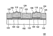
- a cross-sectional example of the semiconductor substrate 101 is shown together with an HBT formed on the island-shaped Ge layer 120.
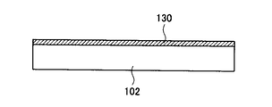
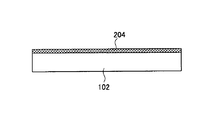
- the cross-sectional example in the manufacture process of the semiconductor substrate 101 is shown.
- the cross-sectional example in the manufacture process of the semiconductor substrate 101 is shown.
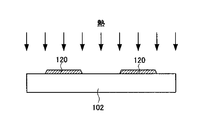
- the cross-sectional example in the manufacture process of the semiconductor substrate 101 is shown.
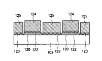
- the cross-sectional example in the manufacture process of the semiconductor substrate 101 is shown.
- the cross-sectional example in the manufacture process of the semiconductor substrate 101 is shown.
- the cross-sectional example in the semiconductor substrate 201 of other embodiment is shown.
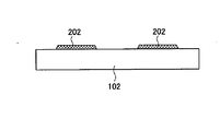
- the cross-sectional example in the manufacturing process of the semiconductor substrate 201 is shown.
- the cross-sectional example in the manufacturing process of the semiconductor substrate 201 is shown.
- the example of a cross section in the semiconductor substrate 301 of other embodiment is shown.
- An example of a cross section in the manufacturing process of the semiconductor substrate 301 is shown.
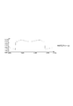
- the cross-sectional shape of the Ge layer which has not been annealed is shown.
- the cross-sectional shape of the Ge layer annealed at 700 ° C. is shown.
- the cross-sectional shape of the Ge layer annealed at 800 ° C. is shown.
- the cross-sectional shape of the Ge layer annealed at 850 degreeC is shown.
- the cross-sectional shape of the Ge layer annealed at 900 ° C. is shown.
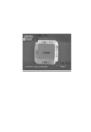
- An electron micrograph of a GaAs crystal formed inside an opening having a side parallel to the ⁇ 010> direction of a Si wafer is shown.
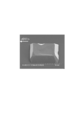
- An electron micrograph of a GaAs crystal formed inside an opening having a side parallel to the ⁇ 010> direction of a Si wafer is shown.
- An electron micrograph of a GaAs crystal formed inside an opening having a side parallel to the ⁇ 011> direction of a Si wafer is shown.
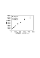
- the film thickness of the GaAs crystal formed inside the opening is shown.
- the relationship between the electrical property of an HBT element and the area of the upper surface of a Ge layer is shown.
- the laser microscope image of a HBT element is shown.
- the laser microscope image of the electronic element containing three HBT elements is shown.
- FIG. 1 shows a plan example of the semiconductor substrate 101 of the present embodiment.
- the semiconductor substrate 101 of this embodiment includes an island-shaped Ge layer 120 on a Si wafer 102.
- the island-shaped Ge layer 120 becomes an element formation region in which elements are formed.
- a plurality of island-shaped Ge layers 120 are formed on the surface of the Si wafer 102 and arranged at equal intervals.
- an HBT heterojunction bipolar transistor
- one electronic element exemplified as the HBT may be formed for each island-shaped Ge layer 120.
- the electronic elements may be connected to each other or may be connected in parallel.
- the Si wafer 102 may be an example of a Si substrate.
- a commercially available Si wafer can be used as the Si wafer 102.
- the Si wafer 102 may be a high-resistance wafer that does not contain impurities, or may be a medium-resistance or low-resistance wafer that contains p-type or n-type impurities.
- the Ge layer 120 may be Ge containing no impurities, or may contain p-type or n-type impurities.
- the surface of the Si wafer 102 may be an example of the main surface of the substrate.
- FIG. 2 shows a cross-sectional example of the semiconductor substrate 101 together with an HBT formed on the island-shaped Ge layer 120.
- the semiconductor substrate 101 includes a Si wafer 102, a Ge layer 120, a buffer layer 122, and an element formation layer 124.
- HBT is formed as an electronic element.
- an HBT is illustrated as an electronic element formed in the element formation layer 124, but is not limited thereto.
- electronic elements such as a light emitting diode, a HEMT (high electron mobility transistor), a solar cell, and a thin film sensor may be formed.
- An HBT collector mesa, emitter mesa, and base mesa are formed on the surface of the element formation layer 124, respectively.
- a collector electrode 108, an emitter electrode 110, and a base electrode 112 are formed on the surfaces of the collector mesa, emitter mesa, and base mesa through contact holes.
- the element formation layer 124 includes a collector layer, an emitter layer, and a base layer of HBT.
- a collector layer As a collector layer, a carrier concentration of 3.0 ⁇ 10 18 cm -3, and n + GaAs layer having a thickness of 500 nm, the carrier concentration of 1.0 ⁇ 10 16 cm -3, a thickness of 500 nm n - and GaAs layer, A laminated film in which the layers are laminated in order from the substrate direction can be exemplified.
- An example of the base layer is a p ⁇ GaAs layer having a carrier concentration of 5.0 ⁇ 10 19 cm ⁇ 3 and a film thickness of 50 nm.
- the Si wafer 102 may be as described above.
- the Ge layer 120 is formed in an isolated island shape on the Si wafer 102.
- the Ge layer 120 is formed by crystal growth on the Si wafer 102.
- An example of crystal growth is epitaxial growth.
- the Ge layer 120 is formed in an island shape having a size not exceeding twice the distance that crystal defects move at the annealing temperature and time.
- the Ge layer 120 may be formed in an island shape having such a size that, when annealed, stress due to a difference in thermal expansion coefficient from the Si wafer 102 as a substrate at the annealing temperature does not cause a defect.
- the Ge layer 120 can be formed in an island shape in which the area of one island Ge layer 120 is 1 mm 2 or less, preferably less than 0.25 mm 2 .
- the Ge layer 120 can be annealed at a temperature and time that allows crystal defects to move, and annealing can be repeated multiple times.
- the plurality of Ge layers 120 may be formed on the Si wafer 102 so as to be separated from each other. Each of the plurality of Ge layers 120 may be arranged at equal intervals.
- the “upper surface” of the Ge layer 120 means a surface of the Ge layer 120 opposite to the surface on the substrate side.
- the surface of the Ge layer 120 that is in contact with the surface of the Si wafer 102 is referred to as the lower surface, and the surface opposite to the lower surface is the upper surface. Called.
- the shape of the upper surface of the Ge layer 120 may be referred to as the upper surface shape.
- the area of the upper surface of each of the plurality of Ge layers 120 may be 1 mm 2 or less, preferably less than 0.25 mm 2 .
- the above area may be a 0.01 mm 2 or less, preferably may be at 1600 .mu.m 2 or less, more preferably be at 900 .mu.m 2 or less.
- the time required for the annealing treatment of the Ge layer 120 can be shortened as compared with the case where the area is larger than 0.01 mm 2 .
- the difference in thermal expansion coefficient between the functional layer and the substrate is large, local warpage tends to occur in the functional layer due to the thermal annealing treatment. Even in such a case, it is possible to suppress the occurrence of crystal defects in the functional layer due to the warpage by setting the area to 0.01 mm 2 or less.
- each Ge layer 120 When the area of the upper surface of each Ge layer 120 is 1600 ⁇ m 2 or less, a high-functional electronic device can be manufactured using the functional layer formed on the Ge layer 120. When the area is 900 ⁇ m 2 or less, the electronic device can be manufactured with high yield.
- the area of the upper surface of each Ge layer 120 may be 25 ⁇ m 2 or more.
- the area is smaller than 25 ⁇ m 2 , when a crystal is epitaxially grown on each Ge layer 120, the growth rate of the crystal becomes unstable and the shape tends to be disturbed. Further, if the area is smaller than 25 ⁇ m 2 , device processing is difficult and the yield may be lowered, which is not industrially preferable.
- the length of one side of the top surface shape may be 100 ⁇ m or less, preferably 80 ⁇ m or less, more preferably 40 ⁇ m or less. More preferably, it may be 30 ⁇ m or less.
- the length of the one side may be the length of the long side.
- the time required for the annealing treatment of the Ge layer 120 can be shortened as compared with the case where the length of one side of the upper surface shape is larger than 100 ⁇ m.
- the difference in thermal expansion coefficient between the functional layer and the substrate is large, the occurrence of crystal defects in the functional layer can be suppressed.
- a high-functional electronic device can be formed using the functional layer formed on each Ge layer 120.
- the electronic device can be manufactured with high yield.
- the Ge layer 120 can be formed by, for example, a CVD method or an MBE method (molecular beam epitaxy method).
- Raw material gas may be GeH 4.
- the Ge layer 120 may be formed by a CVD method under a pressure of 0.1 Pa to 100 Pa.
- the Ge layer 120 may be formed by a CVD method in an atmosphere containing a gas containing a halogen element as a source gas.
- the gas containing a halogen element may be hydrogen chloride gas or chlorine gas.
- the Ge layer 120 may be formed by forming a Ge film on the surface of the Si wafer 102 and patterning the Ge film.
- the Ge film may be formed by the method described above.
- the direction of at least one side of the polygon may be substantially parallel to one of the crystallographic plane orientations of the main surface of the substrate.
- substantially parallel includes the case where the direction of one side of the polygon and one of the crystallographic plane orientations of the substrate are slightly inclined from parallel. The magnitude of the inclination may be 5 ° or less.
- the main surface of the substrate may be a (100) surface, a (110) surface, a (111) surface, or a surface equivalent to these.
- the main surface of the substrate may be slightly inclined from the crystallographic plane orientation. That is, the substrate may have an off angle.
- the magnitude of the inclination may be 10 ° or less.
- the magnitude of the inclination may be preferably 0.05 ° to 6 °, more preferably 0.3 ° to 6 °.
- the main surface of the substrate may be the (100) plane, the (110) plane, or a plane equivalent to these. Thereby, the crystals formed on the Ge layer 120 and the Ge layer 120 are stabilized.
- the main surface of the substrate may be the (100) plane, the (110) plane, or a plane equivalent thereto. As a result, the four-fold symmetric side surface is likely to appear in the crystal.
- the direction of at least one side of the top shape of the Ge layer 120 is selected from the group consisting of the ⁇ 010> direction, the ⁇ 0-10> direction, the ⁇ 001> direction, and the ⁇ 00-1> direction of the Si wafer 102. It may be substantially parallel to any one direction. Thereby, a stable surface appears on the side surface of the GaAs crystal.
- a Ge layer 120 having a hexagonal top surface is formed on the (111) plane of the surface of the Si wafer 102, and a GaAs crystal as the element formation layer 124 is formed on the Ge layer 120.
- the direction of at least one side of the top surface shape of the Ge layer 120 is the ⁇ 1-10> direction, ⁇ 110> direction, ⁇ 0-11> direction, ⁇ 01-1> direction, ⁇ 10 It may be substantially parallel to any one direction selected from the group consisting of a -1> direction and a ⁇ -101> direction. Thereby, a stable surface appears on the side surface of the GaAs crystal.
- the top surface shape of the Ge layer 120 may be a regular hexagon.
- a GaN crystal that is a hexagonal crystal can be formed instead of a GaAs crystal.
- the Ge layer 120 may be annealed at less than 900 ° C., preferably 850 ° C. or less. Thereby, the flatness of the surface of the Ge layer 120 can be maintained. The flatness of the surface of the Ge layer 120 becomes particularly important when another layer is stacked on the surface of the Ge layer 120.
- the Ge layer 120 may be annealed at 680 ° C. or higher, preferably 700 ° C. or higher. Thereby, the density of crystal defects in the Ge layer 120 can be reduced.
- the Ge layer 120 may be annealed under conditions of 680 ° C. or higher and lower than 900 ° C.
- the Ge layer 120 may be annealed in an air atmosphere, a nitrogen atmosphere, an argon atmosphere, or a hydrogen atmosphere.
- an atmosphere containing hydrogen the density of crystal defects in the Ge layer 120 can be reduced while maintaining the surface state of the Ge layer 120 in a smooth state.
- the Ge layer 120 may be annealed under conditions that satisfy the temperature and time at which crystal defects can move.
- crystal defects inside the Ge layer 120 move inside the Ge layer 120 and are captured by, for example, the surface of the Ge layer 120 or a gettering sink inside the Ge layer 120. Thereby, crystal defects near the surface of the Ge layer 120 can be eliminated.
- the surface of the Ge layer 120 or the gettering sink inside the Ge layer 120 may be an example of a defect capturing unit that captures crystal defects that can move inside the Ge layer 120.
- the defect trapping part may be a crystal interface or surface, or a physical scratch.
- the defect trapping portion may be disposed within a distance that the crystal defect can move at the annealing temperature and time.
- the Ge layer 120 may be an example of a seed layer that provides a seed surface for the functional layer.
- Another example of the seed layer is Si x Ge 1-x (where 0 ⁇ x ⁇ 1).
- the annealing may be a two-step annealing in which high-temperature annealing at 800 to 900 ° C. for 2 to 10 minutes and low-temperature annealing at 680 to 780 ° C. for 2 to 10 minutes are repeatedly performed.
- the present invention is not limited to this.
- another layer may be disposed between the Ge layer 120 and the Si wafer 102.
- the other layer may be a single layer or may include a plurality of layers.
- the Ge layer 120 may be formed by the following procedure. First, a seed crystal is formed at a low temperature.
- the seed crystal may be Si x Ge 1-x (where 0 ⁇ x ⁇ 1).
- the growth temperature of the seed crystal may be 330 ° C. or higher and 450 ° C. or lower. After that, the temperature of the Si wafer 102 on which the seed crystal is formed is raised to a predetermined temperature, and then the Ge layer 120 may be formed.
- the surface facing each functional layer of the plurality of Ge layers 120 may be surface-treated with a gas containing P.
- the surface treatment can be performed, for example, by performing an exposure treatment of, for example, PH 3 on the surface of the Ge layer 120 after the Ge layer 120 is formed. Thereby, when the crystal is epitaxially grown on the Ge layer 120, the crystallinity of the crystal is improved.
- the PH 3 treatment may be performed at a temperature of 500 ° C. or higher and 900 ° C. or lower, preferably 600 ° C. or higher and 800 ° C. or lower. If the temperature is lower than 500 ° C., the effect of the treatment may not appear.
- the buffer layer 122 is made of a Group 3-5 compound semiconductor layer that is crystal-grown on the Ge layer 120 and contains P. That is, the buffer layer 122 is formed between the Ge layer 120 and the element formation layer 124.
- a Group 3-5 compound semiconductor layer containing crystal grown P for example, an InGaP layer can be exemplified. Examples of crystal growth include epitaxial growth.
- the buffer layer 122 may be a GaAs layer formed on the Si wafer 102 by crystal growth at a temperature of 500 ° C. or less and formed in an isolated island shape.
- the buffer layer 122 may not be formed between the Ge layer 120 and the element formation layer 124. When the buffer layer 122 is not provided, the surface of the Ge layer 120 facing the element formation layer 124 can be surface-treated with a gas containing P.
- the element formation layer 124 may be an example of a functional layer. As described above, an HBT that may be an example of an electronic element can be formed on the element formation layer 124.
- the element formation layer 124 may be formed in contact with the Ge layer 120. That is, the element formation layer 124 is crystal-grown in contact with the Ge layer 120 or with the buffer layer 122 interposed therebetween. Examples of crystal growth include epitaxial growth.
- the element formation layer 124 may be a group 3-5 compound layer or a group 2-6 compound layer lattice-matched or pseudo-lattice-matched to Ge.
- the element formation layer 124 is a group 3-5 compound layer lattice-matched or pseudo-lattice-matched to Ge, and includes at least one of Al, Ga, and In as a group 3 element, and N, P as a group 5 element , As, and Sb may be included.
- a GaAs layer can be exemplified as the element formation layer 124.
- Pseudo-lattice matching is not perfect lattice matching because the difference between the lattice constants of the two semiconductor layers in contact with each other is small, but it is almost lattice-matched within a range where the occurrence of defects due to lattice mismatch is not significant.
- a state in which two semiconductor layers in contact with each other can be stacked. For example, a stacked state of a Ge layer and a GaAs layer is called pseudo lattice matching.
- the element formation layer 124 may have an arithmetic average roughness (hereinafter also referred to as Ra value) of 0.02 ⁇ m or less, preferably 0.01 ⁇ m or less. Accordingly, a high-functional electronic device can be formed using the element formation layer 124.
- the Ra value is an index representing the surface roughness and can be calculated based on JIS B0601-2001.
- the Ra value can be calculated by folding a roughness curve of a certain length from the center line and dividing the area obtained by the roughness curve and the center line by the measured length.
- the element formation layer 124 is a Group 3-5 compound layer, and includes one or more elements selected from the group consisting of Al, Ga, and In as Group 3 elements, and includes N, P, As, and Sb as Group 5 elements.
- the growth rate of the element formation layer 124 may be 300 nm / min or less, preferably 200 nm / min or less, more preferably 60 nm / min. It may be less than min. Thereby, the Ra value of the element formation layer 124 can be set to 0.02 ⁇ m or less.
- the growth rate of the element formation layer 124 may be 1 nm / min or more, and preferably 5 nm / min or more. Thereby, a high-quality element formation layer 124 can be obtained without sacrificing productivity.
- the element formation layer 124 may be crystal-grown at a growth rate of 1 nm / min to 300 nm / min.
- the element formation layer 124 may be formed on each of the plurality of Ge layers 120.
- a semiconductor substrate including a Si substrate, a plurality of Ge layers 120 formed on the substrate and spaced apart from each other, and a functional layer formed on each of the plurality of Ge layers 120 is obtained.
- each element formation layer 124 may be lattice-matched or pseudo-lattice-matched to each of the plurality of Ge layers 120.
- an electronic element such as HBT may be formed. Accordingly, the Si substrate, the plurality of Ge layers 120 formed on the substrate so as to be spaced apart from each other, the functional layer formed on each of the plurality of Ge layers 120, and the electrons formed on the functional layer An electronic device including the element is obtained.
- One electronic element may be formed for each of the plurality of Ge layers 120.
- the electronic device may be a heterojunction bipolar transistor.
- the electronic elements may be connected to each other. The electronic elements may be connected in parallel.
- an intermediate layer may be disposed between the Ge layer 120 and the element formation layer 124.
- the intermediate layer may be a single layer or may include a plurality of layers.
- the intermediate layer may be formed at 600 ° C. or lower, preferably 550 ° C. or lower. Thereby, the crystallinity of the element formation layer 124 is improved.
- the intermediate layer may be formed at 400 ° C. or higher.
- the intermediate layer may be formed at 400 ° C. or higher and 600 ° C. or lower. Thereby, the crystallinity of the element formation layer 124 is improved.
- the intermediate layer may be a GaAs layer formed at a temperature of 600 ° C. or lower, preferably 550 ° C. or lower.
- the element formation layer 124 may be formed by the following procedure. First, an intermediate layer is formed on the surface of the Ge layer 120. The growth temperature of the intermediate layer may be 600 ° C. or less. Thereafter, the element forming layer 124 may be formed after the temperature of the Si wafer 102 on which the intermediate layer is formed is raised to a predetermined temperature.
- the semiconductor substrate 101 can be manufactured, for example, by forming a plurality of Ge layers 120 spaced from each other on the Si wafer 102 and forming an element formation layer 124 on each of the plurality of Ge layers 120.
- the semiconductor substrate 101 may be manufactured such that each of the plurality of Ge layers 120 and the element formation layer 124 are lattice-matched or pseudo-lattice-matched.
- a GaAs layer may be formed at a temperature of 600 ° C. or less after each of the Ge layers 120 is formed and before the element formation layer 124 is formed.
- the surface of each of the plurality of Ge layers 120 may be treated with a gas containing P.
- 3 to 7 show cross-sectional examples in the manufacturing process of the semiconductor substrate 101.
- a Si wafer 102 is prepared, and a Ge film 130 is formed on the surface of the Si wafer 102 by, for example, epitaxial growth.
- MOCVD metal organic chemical vapor deposition
- MBE molecular beam epitaxy
- GeH 4 can be used as the source gas.
- the Ge film 130 is patterned to form an island-shaped Ge layer 120.
- a photolithography method can be used.
- the patterned Ge layer 120 is subjected to thermal annealing.
- the thermal annealing can be, for example, a two-step annealing in which a high temperature annealing is performed at a temperature that does not reach the melting point of Ge, and then a low temperature annealing is performed at a temperature lower than the temperature of the high temperature annealing.
- the two-step annealing can be repeated a plurality of times. Examples of the temperature and time of the high temperature annealing include 900 ° C. and 10 minutes, and examples of the temperature and time of the low temperature annealing include 780 ° C. and 10 minutes. An example of the number of repetitions is 10 times.
- the two-stage annealing process is repeated a plurality of times on the Ge layer 120 that has been patterned and formed in an island shape. For this reason, crystal defects existing at the stage of epitaxial growth and patterning can be moved to the edge portion of the Ge layer 120 by annealing, and by removing the crystal defects to the edge portion of the Ge layer 120, The crystal defect density can be made extremely low. Thereby, defects caused by, for example, the substrate material of the epitaxial thin film to be formed later can be reduced, and as a result, the performance of the electronic element formed in the element forming layer 124 can be improved. Further, even if the thin film is of a type that cannot be directly grown on the silicon substrate due to lattice mismatch, a high-quality crystalline thin film can be formed using the Ge layer 120 having excellent crystallinity as the substrate material.
- an InGaP layer is grown on the Ge layer 120 as the buffer layer 122.
- crystal growth include epitaxial growth.
- the InGaP layer 123 is also formed on the Si wafer 102 on which the Ge layer 120 is not formed. However, since the InGaP layer 123 is inferior in crystallinity, an electronic element is not formed thereon.
- the InGaP layer 123 may be removed by etching, for example.
- the MOCVD method or the MBE method can be used.
- the source gas TM-Ga (trimethylgallium), TM-In (trimethylindium), and PH 3 (phosphine) can be used.
- a crystalline thin film is formed in a high temperature atmosphere at 650 ° C., for example.
- annealing can also be performed at the stage where the buffer layer 122 shown in FIG. 6 is formed. That is, after the Ge layer 120 is formed, the buffer layer 122 and the InGaP layer 123 can be formed continuously without annealing, and the buffer layer 122 and the Ge layer 120 can be annealed.
- the element formation layer 124 is epitaxially grown on the buffer layer 122, for example.
- an accompanying layer 125 formed simultaneously with the element formation layer 124 is also formed on the InGaP layer 123.
- the accompanying layer 125 may be removed by etching, for example.
- a GaAs layer film including a GaAs layer or InGaAs can be exemplified.
- MOCVD method or MBE method can be used.
- source gas TM-Ga (trimethylgallium), AsH 3 (arsine), or other gases can be used. Examples of the growth temperature include 600 ° C. to 650 ° C.
- the semiconductor substrate 101 shown in FIG. 2 is obtained.
- the semiconductor substrate 101 of this embodiment can be manufactured by the method described above.
- the Ge layer 120 is partitioned by etching, for example, to form an island-shaped Ge layer 120. Then, the Ge layer 120 was subjected to two-stage annealing a plurality of times to increase the crystallinity of the Ge layer 120, and an InGaP layer was formed as the buffer layer 122. Therefore, the semiconductor substrate 101 having a GaAs layer as the element formation layer 124 having excellent crystallinity can be obtained. Since the semiconductor wafer 101 employs the Si wafer 102, the semiconductor substrate 101 can be manufactured at low cost, and the heat generated by the electronic elements formed in the element formation layer 124 can be efficiently exhausted.
- the annealing process for the Ge layer 120 described in FIG. 5 is not essential. Even if the Ge layer 120 is not annealed, the buffer layer 122 can provide a certain degree of crystallinity improvement effect.
- FIG. 8 shows a cross-sectional example of the semiconductor substrate 201 of another embodiment.
- the semiconductor substrate 201 is substantially the same as the semiconductor substrate 101 except that a Ge layer 120 is not used and a GaAs layer crystal-grown at a temperature of 500 ° C. or lower is used as the buffer layer 202. In the following description, differences from the semiconductor substrate 101 will be described.
- FIG. 9 and 10 show cross-sectional examples in the process of manufacturing the semiconductor substrate 201.
- a Si wafer 102 is prepared, and a GaAs film 204 is crystal-grown on the surface of the Si wafer 102 at a temperature of 500 ° C. or lower.
- the MOCVD method or the MBE method can be used to form the GaAs film 204.
- the source gas TE-Ga (triethylgallium) or AsH 3 (arsine) can be used.
- An example of the growth temperature is 450 ° C.
- the GaAs film 204 is etched by photolithography to form the buffer layer 202 in an isolated island shape. Subsequent steps may be the same as those of the semiconductor substrate 101.
- the semiconductor substrate 201 In the semiconductor substrate 201, a GaAs layer formed at a temperature of 500 ° C. or lower is applied as the buffer layer 202. Even in the buffer layer 202 made of a GaAs layer grown at a low temperature, the crystallinity of the element formation layer 124 is improved to some extent. Therefore, the same effects as those of the semiconductor substrate 101 can be obtained, in which the semiconductor substrate 201 can be provided at low cost and the performance of the electronic element formed in the element formation layer 124 can be improved.
- FIG. 11 shows a cross-sectional example of a semiconductor substrate 301 of still another embodiment.
- the surface of the Si wafer 102 is surface-treated with a gas containing P.
- FIG. 12 shows a cross-sectional example in the process of manufacturing the semiconductor substrate 301.
- the surface of the Si wafer 102 is subjected to, for example, PH 3 exposure treatment.
- the exposure process may be performed in a high temperature atmosphere, and PH 3 may be activated by plasma or the like.
- a GaAs film to be the element formation layer 124 is grown on the surface of the Si wafer 102 subjected to the PH 3 exposure treatment, and the element formation layer 124 is formed in an isolated island shape by etching, for example, by photolithography. it can.
- the semiconductor substrate similar to the semiconductor substrate 201 shown in FIG. 8 can be formed by continuing the steps after the step shown in FIG. That is, the surface of the semiconductor substrate 201 may be subjected to, for example, PH 3 exposure treatment, and the GaAs film 204 can be crystal-grown at a temperature of 500 ° C. or lower, and then the GaAs film 204 may be patterned to form an island-shaped GaAs layer.
- the buffer layer 202 can be formed.
- the crystallinity of the GaAs layer as the element formation layer 124 is good. I was able to. Therefore, the same effect as the case of the semiconductor substrate 101 that the semiconductor substrate can be provided at low cost and the performance of the electronic element formed in the element formation layer 124 can be obtained.
- Example 1 The following experiment was conducted for the purpose of examining the influence of the annealing temperature on the flatness of the surface of the Ge layer. The experiment was performed by annealing the Ge layer formed on the surface of the Si wafer and observing the cross-sectional shape of the annealed Ge layer. By conducting the above experiment for cases where the annealing temperature was different, the influence of the annealing temperature on the surface flatness of the Ge layer was examined.
- the Ge layer was formed by the following procedure. First, a SiO 2 layer was formed on the surface of the Si wafer by a thermal oxidation method. A commercially available single crystal Si substrate was used as the Si wafer. An opening was formed in the SiO 2 layer by etching. The planar shape of the SiO 2 layer was a square having a side length of 400 ⁇ m.
- “flat shape” of the SiO 2 layer which means the shape of the case where the projection of the SiO 2 layer on the main surface of the substrate.
- the “bottom shape” of the opening means the shape of the opening on the Si wafer side surface of the SiO 2 layer in which the opening is formed.
- GeH 4 was used as the source gas.
- the flow rate of the source gas and the film formation time were set to predetermined values, respectively.
- FIG. 13 to 17 show the relationship between the annealing temperature and the flatness of the Ge layer.
- FIG. 13 shows the cross-sectional shape of an unannealed Ge layer.
- FIGS. 14, 15, 16 and 17 show cross-sectional shapes of the Ge layer when annealing is performed at 700 ° C., 800 ° C., 850 ° C., and 900 ° C., respectively.
- the cross-sectional shape of the Ge layer was observed with a laser microscope.
- the vertical axis in each figure indicates the distance in the direction perpendicular to the main surface of the Si wafer, and indicates the thickness of the Ge layer.
- the horizontal axis of each figure shows the distance in the direction parallel to the main surface of the Si wafer.
- the lower the annealing temperature the better the flatness of the surface of the Ge layer.
- the annealing temperature is less than 900 ° C., it can be seen that the surface of the Ge layer exhibits excellent flatness.
- Example 2 The following experiment was conducted for the purpose of investigating the influence of the relationship between the top surface shape of the Ge layer and the crystallographic orientation of the substrate on the crystal formed on the Ge layer.
- the experiment was performed by forming a Ge layer on the (100) plane of the Si wafer, growing a GaAs crystal on the Ge layer, and observing the shape of the GaAs crystal.
- the relationship between the top surface shape of the Ge layer and the crystallographic orientation of the substrate is The effect on the crystals formed on the substrate was investigated.
- the Ge layer was formed by the following procedure. First, a SiO 2 layer was formed on the surface of the Si wafer. A commercially available single crystal Si substrate was used as the Si wafer. The plane orientation of the surface of the Si wafer was the (100) plane of Si. The SiO 2 layer was patterned into a predetermined shape by etching. Three or more SiO 2 layers having the predetermined size were formed on the surface of the Si wafer. The SiO 2 layer was formed so that the SiO 2 layers having the predetermined size were arranged at equal intervals of 500 ⁇ m. An opening having a predetermined bottom shape was formed in the SiO 2 layer by etching.
- the opening was formed so that the direction of one side of the bottom shape was parallel to the ⁇ 010> direction or the ⁇ 011> direction of the Si wafer.
- the opening was formed so that the direction of the long side was parallel to the ⁇ 010> direction or the ⁇ 011> direction of the Si wafer.
- a Ge layer was selectively grown inside the opening by CVD.
- GeH 4 was used as the source gas.
- the flow rate of the source gas and the film formation time were set to predetermined values, respectively.
- a GaAs crystal was formed on the annealed Ge layer by MOCVD.
- the GaAs crystal was epitaxially grown on the surface of the Ge layer inside the opening under the conditions of 620 ° C. and 8 MPa.
- Trimethyl gallium and arsine were used as source gases.
- the flow rate of the source gas and the film formation time were set to predetermined values, respectively.
- GaAs crystals were formed by changing the positional relationship between the crystallographic orientation of the Si wafer and the shape of the bottom of the opening. In each case, the surface state of the formed GaAs crystal was observed with an electron microscope. 18 to 20 show electron micrographs of the surface of the GaAs crystal formed on the Ge layer.
- FIG. 18 shows a case where an opening is formed in the SiO 2 layer so that the direction of one side of the opening and the ⁇ 010> direction of the Si wafer are substantially parallel, and then a GaAs crystal is grown inside the opening.
- the planar shape of the SiO 2 layer was a square having a side length of 300 ⁇ m.
- the bottom shape of the opening was a square having a side of 10 ⁇ m.
- the arrow in the figure indicates the ⁇ 010> direction.
- a crystal having a uniform shape was obtained.
- the (10-1) plane, the (1-10) plane, the (101) plane, and the (110) plane appear on the four side surfaces of the GaAs crystal, respectively.
- the (11-1) plane appears in the upper left corner of the GaAs crystal
- the (1-11) plane appears in the lower right corner of the GaAs crystal in the figure. Recognize.
- the (11-1) plane and the (1-11) plane are equivalent planes to the (-1-1-1) plane and are stable planes.
- FIG. 19 shows the results when observed obliquely from above at an angle of 45 °.
- the planar shape of the SiO 2 layer was a square having a side length of 50 ⁇ m.
- the bottom shape of the opening was a square having a side length of 10 ⁇ m.
- the arrow in the figure indicates the ⁇ 010> direction.
- crystals with a well-formed shape were obtained.
- FIG. 20 after forming an opening in the SiO 2 layer so that the direction of one side of the opening is substantially parallel to the ⁇ 011> direction of the Si wafer, a GaAs crystal is grown inside the opening.
- the planar shape of the SiO 2 layer was a square having a side length of 400 ⁇ m.
- the bottom shape of the opening was a square having a side length of 10 ⁇ m.
- the arrow in the figure indicates the ⁇ 011> direction.
- FIG. 20 compared with FIG. 18 and FIG. 19, a crystal with a disordered shape was obtained.
- As a result of the appearance of a relatively unstable (111) plane on the side surface of the GaAs crystal it is considered that the shape of the crystal is disturbed.
- Example 3 The following experiment was conducted for the purpose of examining the relationship between the growth rate of the crystal formed on the Ge layer and the surface roughness of the crystal.
- a GaAs crystal is grown on the Ge layer, and the film thickness of the GaAs crystal grown for a predetermined time and the cross-sectional shape of the GaAs crystal are observed. It was carried out.
- the influence of the growth rate of the GaAs crystal on the surface roughness of the GaAs crystal was investigated.
- a Ge layer and a GaAs crystal were formed on the Si wafer by the same procedure as in Experimental Example 2.
- the length of one side of the planar shape of the SiO 2 layer is, 200 ⁇ m, 500 ⁇ m, 700 ⁇ m, 1000 ⁇ m , 1500 ⁇ m, 2000 ⁇ m, was set to be 3000 ⁇ m or 4250Myuemu.
- the SiO 2 layer was formed so that the periphery of the SiO 2 layer was surrounded by the surface of the Si wafer when viewed from above the Si wafer.
- the experiment was performed for three cases, in which the shape of the bottom of the opening was a square with a side of 10 ⁇ m, a square with a side of 20 ⁇ m, a rectangle with a short side of 30 ⁇ m and a long side of 40 ⁇ m.
- the opening was formed so that the direction of one side of the bottom shape of the opening was parallel to the ⁇ 010> direction of the Si wafer.
- the bottom shape was a rectangle
- the opening was formed so that the direction of the long side was parallel to the ⁇ 010> direction of the Si wafer.
- the growth conditions of the Ge layer and the GaAs crystal were set to the same conditions as in Experimental Example 2.
- GaAs crystals were formed by changing the planar shape of the SiO 2 layer and the bottom shape of the opening.
- the film thickness of the GaAs crystal is measured by measuring the film thickness at three measurement points of the GaAs crystal with a needle-type step gauge (manufactured by KLA Tencor, Surface Profiler P-10), and averaging the film thicknesses at the three positions.
- the cross-sectional shape of the GaAs crystal was observed with a laser microscope apparatus.
- the said film thickness measures the film thickness in three measurement points of the element formation layer 124 directly by the cross-sectional observation method by a transmission electron microscope or a scanning electron microscope, and averages the film thickness of the said three places. You may calculate by.
- Example 4 The following experiment was conducted for the purpose of examining the relationship between the growth rate of the crystal formed on the Ge layer and the surface roughness of the crystal. The experiment was carried out in the same manner as in Experimental Example 3 except that the supply amount of trimethylgallium was halved and the growth rate of the GaAs crystal was halved.
- the length of one side of the planar shape of the SiO 2 layer was set to be 200 [mu] m, 500 [mu] m, 1000 .mu.m, 2000 .mu.m, and 3000 ⁇ m or 4250Myuemu.
- the experiment was performed in the case where the bottom shape of the opening was a square having a side of 10 ⁇ m.
- GaAs crystals were formed by changing the planar shape of the SiO 2 layer.
- the thickness of the GaAs crystal formed during a certain time and the cross-sectional shape of the GaAs crystal were observed.
- the SiO 2 layer was removed after the GaAs crystal was formed. The film thickness and cross-sectional shape of the GaAs crystal were observed in the same manner as in Experimental Example 3.
- FIG. 21 shows the average value of the thickness of the GaAs crystal in each case of Experimental Example 3.
- Table 1 shows the growth rate of the GaAs crystal and the Ra value in each of Experimental Example 3 and Experimental Example 4.
- the SiO 2 layer may be referred to as a covering region.
- the length of one side of the bottom shape of the opening may be referred to as the length of one side of the opening.
- the length of one side of the planar shape of the SiO 2 layer, the length of one side of the SiO 2 layer, or may be referred to as the length of a side of the covering region.
- FIG. 21 shows the relationship between the growth rate of the GaAs crystal and the planar shape of the SiO 2 layer and the planar shape of the opening.
- the vertical axis indicates the film thickness of the GaAs crystal grown for a certain time
- the horizontal axis indicates the length [ ⁇ m] of one side of the SiO 2 layer.
- the film thickness of the GaAs crystal is a film thickness grown for a fixed time, and thus an approximate value of the growth rate of the GaAs crystal can be obtained by dividing the film thickness by the time.
- the rhombus plot shows experimental data when the bottom shape of the opening is a square having a side of 10 ⁇ m
- the square plot shows experimental data when the bottom shape of the opening is a square having a side of 20 ⁇ m.
- a triangular plot shows experimental data when the bottom shape of the opening is a rectangle having a long side of 40 ⁇ m and a short side of 30 ⁇ m.
- FIG. 21 shows that the growth rate stably increases as the size of the SiO 2 layer increases until the length of one side of the SiO 2 layer reaches 4250 ⁇ m.
- Table 1 shows the growth rate [ ⁇ / min] of the GaAs crystal and the Ra value [ ⁇ m] in each of Experimental Example 3 and Experimental Example 4.
- the film thickness of the GaAs crystal was measured with a needle type step gauge.
- Ra value was computed based on the observation result by a laser microscope apparatus. Table 1 shows that the surface roughness improves as the growth rate of the GaAs crystal decreases. It can be seen that the Ra value is 0.02 ⁇ m or less when the growth rate of the GaAs crystal is 300 nm / min or less.
- Example 5 The following experiment was conducted for the purpose of investigating the influence of the shape of the upper surface of the Ge layer on the characteristics and yield of an electronic device using a functional layer formed on the Ge layer. The experiment was performed by fabricating an HBT element using a functional layer formed on the Ge layer and measuring the base sheet resistance value R b [ ⁇ / ⁇ ] and the current amplification factor ⁇ of the HBT element. By conducting the above experiment for the case where the upper surface area of the Ge layer was different, the influence of the upper surface shape of the Ge layer on the characteristics and yield of the electronic device was examined.
- the HBT element was manufactured by the following procedure. First, a semiconductor substrate provided with a Si wafer, a Ge layer, and a GaAs layer as an element formation layer was produced. Next, a semiconductor layer was formed on the manufactured semiconductor substrate to manufacture an HBT element.
- the semiconductor substrate was produced by the following procedure. First, in the same manner as in Experimental Example 3, a SiO 2 layer was formed on the surface of the Si wafer, and a Ge layer was formed inside the opening provided in the SiO 2 layer. After forming the Ge layer, annealing was performed.
- the shape of the bottom of the opening is a square with a side of 20 ⁇ m, a rectangle with a short side of 20 ⁇ m and a long side of 40 ⁇ m, a square with a side of 30 ⁇ m, a rectangle with a short side of 30 ⁇ m and a long side of 40 ⁇ m, An HBT element was produced for each of the rectangles having a short side of 20 ⁇ m and a long side of 80 ⁇ m.
- the bottom shape of the opening is a square
- one of the two orthogonal sides of the bottom shape is parallel to the ⁇ 010> direction of the Si wafer, and the other is parallel to the ⁇ 001> direction of the Si wafer.
- An opening was formed.
- the bottom shape of the opening is rectangular, the opening is formed so that the long side of the bottom shape is parallel to the ⁇ 010> direction of the Si wafer and the short side is parallel to the ⁇ 001> direction of the Si wafer. did.
- the planar shape of the SiO 2 layer was mainly tested in the case of a square having a side of 300 ⁇ m.
- an intermediate layer was formed between the Ge layer and the GaAs layer.
- the intermediate layer was formed on the Ge layer by MOCVD after annealing the Ge layer.
- the intermediate layer was formed by setting the temperature of the Si wafer on which the Ge layer was formed to be 550 ° C.
- the intermediate layer was grown using trimethylgallium and arsine as source gases.
- the film thickness of the intermediate layer was 30 nm.
- a GaAs layer was formed by MOCVD.
- the thickness of the GaAs layer was 500 nm.
- a semiconductor layer was stacked on the surface of the GaAs layer by MOCVD. Accordingly, the Si wafer, the Ge layer having a thickness of 850 nm, the intermediate layer having a thickness of 30 nm, the undoped GaAs layer having a thickness of 500 nm, the n-type GaAs layer having a thickness of 300 nm, and the thickness of 20 nm.
- An HBT element structure was obtained in which an n-type GaAs layer having a thickness of 120 nm and an n-type InGaAs layer having a thickness of 60 nm were arranged in this order.
- Si was used as an n-type impurity.
- C was used as a p-type impurity.
- An electrode was arranged on the obtained HBT element structure to produce an HBT element.
- the bottom shape of the opening was changed to produce an HBT element.
- the base sheet resistance value R b [ ⁇ / ⁇ ] and the current amplification factor ⁇ of the manufactured HBT element were measured.
- the current amplification factor ⁇ was obtained by dividing the collector current value by the base current value.
- FIG. 22 shows the relationship between the ratio of the current amplification factor ⁇ to the base sheet resistance value Rb of the HBT element and the area [ ⁇ m 2 ] of the planar shape of the opening.
- the area of the upper surface of the Ge layer substantially coincided with the area of the bottom shape of the opening. Further, the length of one side of the top shape of the Ge layer substantially coincided with the length of one side of the bottom shape of the opening.
- the vertical axis represents a value obtained by dividing the current amplification factor ⁇ by the base sheet resistance value R b [ ⁇ / ⁇ ], and the horizontal axis represents the area of the bottom shape of the opening.
- the value of the current amplification factor ⁇ is not shown in FIG. 22, a high value of about 70 to 100 was obtained for the current amplification factor.
- the current amplification factor ⁇ was 10 or less.
- a device having excellent electrical characteristics can be produced by locally forming the HBT element structure on the surface of the Si wafer.
- the length of one side of the top shape of the Ge layer is 80 ⁇ m or less, or the area of the top surface of the Ge layer is 1600 ⁇ m 2 or less, it can be seen that a device having excellent electrical characteristics can be manufactured.
- FIG. 23 shows a laser microscope image of the obtained HBT element.
- the light gray portion indicates the electrode.
- three electrodes are lined up in the opening region arranged near the center of the square covering region.
- the three electrodes respectively indicate a base electrode, an emitter electrode, and a collector electrode of the HBT element from the left in the figure.
- transistor operation was confirmed. Further, when the cross section of the HBT element was observed with a transmission electron microscope, no dislocation was observed.
- Example 6 In the same manner as in Experimental Example 5, three HBT elements having the same structure as in Experimental Example 5 were produced. The three HBT elements thus produced were connected in parallel to produce an electronic element.
- the planar shape of the SiO 2 layer was a rectangle having a long side of 100 ⁇ m and a short side of 50 ⁇ m.
- three openings were provided in the SiO 2 layer. All of the bottom shapes of the openings were squares having a side of 15 ⁇ m.
- the semiconductor substrate was formed under the same conditions as in Experimental Example 5.
- FIG. 24 shows a laser microscope image of the obtained electronic element.
- the light gray portion indicates the electrode.
- FIG. 24 shows that three HBT elements are connected in parallel. When the electrical characteristics of the electronic device were measured, transistor operation was confirmed.
- a crystal thin film having excellent crystallinity can be formed on an inexpensive silicon substrate, and a semiconductor substrate, an electronic device, or the like can be formed using the crystal thin film.
Landscapes
- Recrystallisation Techniques (AREA)
- Bipolar Transistors (AREA)
- Bipolar Integrated Circuits (AREA)
Abstract
Description
Hsin-Chiao Luan et.al.、「High-quality Ge epilayers on Si with low threading-dislocation densities」、APPLIED PHYSICS LETTERS、VOLUME 75, NUMBER 19、8 NOVEMBER 1999.
アニール温度がGe層の表面の平坦性に与える影響を調べる目的で、以下の実験を実施した。実験は、Siウェハの表面に形成されたGe層をアニール処理して、アニール処理されたGe層の断面形状を観察することで実施した。アニール処理の温度が異なる場合について上記の実験を実施することで、アニール温度がGe層の表面の平坦性に与える影響を調べた。
Ge層の上面形状と基板の結晶学的方位との関係が、当該Ge層の上に形成される結晶に与える影響を調べる目的で、以下の実験を実施した。実験は、Siウェハの(100)面にGe層を形成した後、Ge層の上にGaAs結晶を成長させ、当該GaAs結晶の形状を観察することで実施した。Ge層の上面形状とSiウェハの結晶学的方位との位置関係が異なる場合について上記の実験を実施することで、Ge層の上面形状と基板の結晶学的方位との関係が、当該Ge層の上に形成される結晶に与える影響を調べた。
Ge層の上に形成された結晶の成長速度と、当該結晶の表面粗さとの関係を調べる目的で、以下の実験を実施した。実験は、Siウェハの表面にGe層を形成した後、Ge層の上にGaAs結晶を成長させ、一定時間の間に成長したGaAs結晶の膜厚と、当該GaAs結晶の断面形状とを観察することで実施した。GaAs結晶の成長速度が異なる場合について上記の実験を実施することで、GaAs結晶の成長速度がGaAs結晶の表面粗さに与える影響を調べた。
Ge層の上に形成された結晶の成長速度と、当該結晶の表面粗さとの関係を調べる目的で、以下の実験を実施した。トリメチルガリウムの供給量を半分にして、GaAs結晶の成長速度を約半分にした以外は実験例3の場合と同様にして、実験を実施した。なお、本実験例においては、SiO2層をパターニングする工程において、SiO2層の平面形状の一辺の長さが、200μm、500μm、1000μm、2000μm、3000μmまたは4250μmとなるように設定した。また、開口の底面形状が、一辺が10μmの正方形の場合について、実験を実施した。

Ge層の上面形状が、Ge層の上に形成した機能層を利用した電子デバイスの特性および歩留まりに与える影響を調べる目的で、以下の実験を実施した。実験は、Ge層の上に形成した機能層を用いてHBT素子を作製して、HBT素子のベースシート抵抗値Rb[Ω/□]と電流増幅率βとを測定することで実施した。Ge層の上面の面積の大きさが異なる場合について上記の実験を実施することで、Ge層の上面形状が、上記電子デバイスの特性および歩留まりに与える影響を調べた。
実験例5と同様にして、実験例5と同様の構造を有するHBT素子を3つ作製した。作製した3つのHBT素子を並列接続して電子素子を作製した。本実験例では、SiO2層の平面形状は、長辺が100μm、短辺が50μmの長方形であった。また、上記SiO2層の内部に、3つの開口を設けた。開口の底面形状は、すべて、一辺が15μmの正方形であった。それ以外の条件については、実験例5の場合と同一の条件で半導体基板をした。
Claims (62)
- Siの基板と、
前記基板上に結晶成長され、孤立した島状に形成されたGe層と、
前記Ge層の上に結晶成長され、Pを含む3-5族化合物半導体層からなるバッファ層と、
前記バッファ層の上に結晶成長された機能層と、
を備える半導体基板。 - Siの基板と、
前記基板上に、500℃以下の温度で結晶成長され、孤立した島状に形成されたGaAs層からなるバッファ層と、
前記バッファ層の上に結晶成長された機能層と、
を備える半導体基板。 - Siの基板と、
前記基板上に結晶成長され、孤立した島状に形成された機能層と、
を備え、
前記基板の表面は、Pを含むガスにより表面処理された、半導体基板。 - 前記Ge層は、アニールした場合に、前記アニールの温度および時間において結晶欠陥が移動する距離の2倍を越えない大きさの島状に形成される、
請求項1に記載の半導体基板。 - 前記Ge層は、アニールした場合に、前記アニールの温度において前記基板であるSiとの熱膨張係数の相違によるストレスが欠陥を発生させない大きさの島状に形成される、
請求項1に記載の半導体基板。 - 前記Ge層は、面積が1mm2以下の島状に形成される、
請求項1に記載の半導体基板。 - 前記Ge層は、結晶欠陥が移動できる温度および時間でアニールされてなる、
請求項1、請求項4、請求項5または請求項6の何れか一項に記載の半導体基板。 - 前記アニールは、複数回繰り返される、
請求項7に記載の半導体基板。 - 前記機能層は、Geに格子整合または擬格子整合する、3-5族化合物層または2-6族化合物層である、
請求項1、請求項4、請求項5、請求項6、請求項7または請求項8の何れか一項に記載の半導体基板。 - 前記機能層は、Geに格子整合または擬格子整合する、3-5族化合物層であり、3族元素としてAl、Ga、Inのうち少なくとも1つを含み、5族元素としてN、P、As、Sbのうち少なくとも1つを含む、
請求項1、請求項4、請求項5、請求項6、請求項7または請求項8の何れか一項に記載の半導体基板。 - Siの基板と、
前記基板の上に、互いに離間して形成された複数のGe層と、
前記複数のGe層の各々の上に形成されたバッファ層と、
前記バッファ層の上に形成された機能層と、
を含む半導体基板。 - 前記バッファ層は、前記複数のGe層の各々に格子整合または擬格子整合し、
前記機能層は、前記バッファ層に格子整合または擬格子整合している、
請求項11に記載の半導体基板。 - 前記バッファ層は、Pを含む3-5族化合物半導体層を含む、
請求項11または請求項12に記載の半導体基板。 - 前記複数のGe層の各々は、水素を含む雰囲気中でアニールされてなる、
請求項11から請求項13までの何れか一項に記載の半導体基板。 - 前記複数のGe層の各々の前記機能層に対向する面は、Pを含むガスにより表面処理されている、
請求項11から請求項14までの何れか一項に記載の半導体基板。 - 前記複数のGe層の各々の上面の面積は、1mm2以下である、
請求項11から請求項15までの何れか一項に記載の半導体基板。 - 前記複数のGe層の各々の上面の面積は、1600μm2以下である、
請求項16に記載の半導体基板。 - 前記複数のGe層の各々の上面の面積は、900μm2以下である、
請求項17に記載の半導体基板。 - 前記複数のGe層の各々の上面は、長方形であり、
前記長方形の長辺は、80μm以下である、
請求項16に記載の半導体基板。 - 前記複数のGe層の各々の上面は、長方形であり、
前記長方形の長辺は、40μm以下である、
請求項17に記載の半導体基板。 - 前記基板の主面が(100)面であり、
前記複数のGe層の各々の上面は、正方形または長方形であり、
前記正方形または前記長方形の少なくとも1辺の方向は、前記主面における<010>方向、<0-10>方向、<001>方向および<00-1>方向からなる群から選択された何れか一つの方向と実質的に平行である、
請求項11から請求項20までの何れか一項に記載の半導体基板。 - 前記基板の主面が(111)面であり、
前記複数のGe層の各々の上面は、六角形であり、
前記六角形の少なくとも1辺の方向は、前記主面における<1-10>方向、<-110>方向、<0-11>方向、<01-1>方向、<10-1>方向および<-101>方向からなる群から選択された何れか一つの方向と実質的に平行である、
請求項11から請求項20までの何れか一項に記載の半導体基板。 - Siの基板と、
前記基板の上に、互いに離間して形成された複数のバッファ層であって、GaAs層を含む複数のバッファ層と、
前記複数のバッファ層の各々の上に形成された機能層と、
を含む半導体基板。 - 前記機能層は、前記複数のバッファ層の各々に格子整合または擬格子整合している、
請求項23に記載の半導体基板。 - 前記GaAs層は、600℃以下の温度で結晶成長されてなる、
請求項23または請求項24に記載の半導体基板。 - Siの基板と、
前記基板の上に、互いに離間して形成された複数の機能層と、
を含み、
前記基板の表面は、前記機能層の形成前に、Pを含むガスにより表面処理されている、半導体基板。 - 前記機能層は、3-5族化合物層または2-6族化合物層である、
請求項11から請求項26までの何れか一項に記載の半導体基板。 - 前記機能層は、3-5族化合物層であり、3族元素としてAl、GaおよびInからなる群から選択された1以上の元素を含み、5族元素としてN、P、AsおよびSbからなる群から選択された1以上の元素を含む、
請求項11から請求項26までの何れか一項に記載の半導体基板。 - 前記機能層の算術平均粗さは、0.02μm以下である、
請求項28に記載の半導体基板。 - Siの基板の上に、Ge層を結晶成長する段階と、
前記Ge層をパターニングして、孤立した島状のGe層を形成する段階と、
前記Ge層の上に、Pを含む3-5族化合物半導体層からなるバッファ層を結晶成長する段階と、
前記バッファ層の上に機能層を結晶成長する段階と、
を備えた半導体基板の製造方法。 - 前記島状のGe層を、結晶欠陥が移動できる温度および時間でアニールする段階、
をさらに備える請求項30に記載の半導体基板の製造方法。 - 前記アニールを、複数回繰り返す段階、
をさらに備える請求項31に記載の半導体基板の製造方法。 - Siの基板の上に、互いに離間した複数のGe層を形成する段階と、
前記複数のGe層の各々の上に、バッファ層を形成する段階と、
前記バッファ層の上に、機能層を形成する段階と、
を含む半導体基板の製造方法。 - 前記バッファ層を形成する段階において、前記バッファ層を前記Ge層に格子整合または擬格子整合させ、
前記機能層を形成する段階において、前記機能層を前記バッファ層に格子整合または擬格子整合させる、
請求項33に記載の半導体基板の製造方法。 - 前記バッファ層を形成する段階は、Pを含む3-5族化合物半導体層を形成する段階を含む、
請求項33または請求項34記載の半導体基板の製造方法。 - 前記複数のGe層の各々を、結晶欠陥が移動できる温度および時間でアニールする段階、をさらに含む、
請求項33から請求項35までの何れか一項に記載の半導体基板の製造方法。 - 前記アニールする段階は、前記複数のGe層の各々を、680℃以上900℃未満の温度でアニールする、
請求項36に記載の半導体基板の製造方法。 - 前記アニールする段階は、前記複数のGe層の各々を、水素を含む雰囲気中でアニールする、
請求項36または請求項37に記載の半導体基板の製造方法。 - 前記アニールする段階を、複数含む、
請求項36から請求項38までの何れか一項に記載の半導体基板の製造方法。 - Siの基板の上に、互いに離間した複数のバッファ層であってGaAs層を含む複数のバッファ層を形成する段階と、
前記複数のバッファ層の各々の上に、機能層を形成する段階と、
を含む半導体基板の製造方法。 - 前記GaAs層は、600℃以下の温度で結晶成長される、
請求項40に記載の半導体基板の製造方法。 - Siの基板の表面を、Pを含むガスにより表面処理する段階と、
前記基板の上に、互いに離間した複数の機能層を形成する段階と、
を含む半導体基板の製造方法。 - 前記機能層は、3-5族化合物層であり、3族元素としてAl、GaおよびInからなる群から選択された1以上の元素を含み、5族元素としてN、P、AsおよびSbからなる群から選択された1以上の元素を含み、
前記機能層を形成する段階は、前記機能層を、1nm/min以上、300nm/min以下の成長速度で結晶成長させる、
請求項33から請求項42までの何れか一項に記載の半導体基板の製造方法。 - Siの基板と、
前記基板上に結晶成長され、孤立した島状に形成されたGe層と、
前記Ge層の上に結晶成長され、Pを含む3-5族化合物半導体層からなるバッファ層と、
前記バッファ層の上に結晶成長された機能層と、
前記機能層に形成された電子素子と、
を備える電子デバイス。 - 前記電子素子は、前記島状のGe層ごとに一つ形成されている、
請求項44に記載の電子デバイス。 - 前記島状のGe層は、前記基板の上に複数形成され、複数の前記島状のGe層は、等間隔に配置される、
請求項44または請求項45に記載の電子デバイス。 - Siの基板と、
前記基板の上に、互いに離間して形成された複数のGe層と、
前記複数のGe層の各々の上に形成されたバッファ層と、
前記バッファ層の上に形成された機能層と、
前記機能層に形成された電子素子と、
を含む電子デバイス。 - 前記バッファ層は、前記複数のGe層の各々に格子整合または擬格子整合され、
前記機能層は、前記バッファ層に格子整合または擬格子整合されている、
請求項47に記載の電子デバイス。 - 前記バッファ層は、Pを含む3-5族化合物半導体層を含む、
請求項47または請求項48に記載の電子デバイス。 - 前記電子素子は、前記Ge層ごとに一つずつ形成されている、
請求項47から請求項49までの何れか一項に記載の電子デバイス。 - 前記複数のGe層の各々は、等間隔に配置されている、
請求項47から請求項50までの何れか一項に記載の電子デバイス。 - Siの基板と、
前記基板の上に、互いに離間して形成された複数のバッファ層であって、GaAs層を含む複数のバッファ層と、
前記複数のバッファ層の各々の上に形成された機能層と、
前記機能層に形成された電子素子と、
を含む電子デバイス。 - 前記機能層は、前記複数のバッファ層の各々に格子整合または擬格子整合されている、
請求項52に記載の電子デバイス。 - 前記GaAs層は、600℃以下の温度で結晶成長されている、
請求項52または請求項53に記載の電子デバイス。 - 前記電子素子は、前記バッファ層ごとに一つずつ形成されている、
請求項52から請求項54までの何れか一項に記載の電子デバイス。 - 前記複数のバッファ層の各々は、等間隔に配置されている、
請求項52から請求項55までの何れか一項に記載の電子デバイス。 - Siの基板と、
前記基板の上に、互いに離間して形成された複数の機能層と、
前記機能層に形成された電子素子と、
を含み、
前記基板の表面は、前記機能層の形成前に、Pを含むガスにより表面処理されている、
電子デバイス。 - 前記電子素子は、前記機能層ごとに一つずつ形成されている、
請求項57に記載の電子デバイス。 - 前記複数の機能層の各々は、等間隔に配置されている、
請求項57または請求項58に記載の電子デバイス。 - 前記電子素子は、ヘテロジャンクションバイポーラトランジスタである、
請求項44から請求項59までの何れか一項に記載の電子デバイス。 - 前記電子素子が、相互に接続されている、
請求項44から請求項60までの何れか一項に記載の電子デバイス。 - 前記電子素子が、並列に接続されている、
請求項44から請求項51までの何れか一項に記載の電子デバイス。
Priority Applications (2)
| Application Number | Priority Date | Filing Date | Title |
|---|---|---|---|
| CN2008801199956A CN101896999B (zh) | 2007-12-28 | 2008-12-26 | 半导体基板、半导体基板的制造方法及电子器件 |
| US12/811,038 US8809908B2 (en) | 2007-12-28 | 2008-12-26 | Semiconductor wafer, semiconductor wafer manufacturing method, and electronic device |
Applications Claiming Priority (2)
| Application Number | Priority Date | Filing Date | Title |
|---|---|---|---|
| JP2007-341295 | 2007-12-28 | ||
| JP2007341295 | 2007-12-28 |
Publications (1)
| Publication Number | Publication Date |
|---|---|
| WO2009084239A1 true WO2009084239A1 (ja) | 2009-07-09 |
Family
ID=40823975
Family Applications (1)
| Application Number | Title | Priority Date | Filing Date |
|---|---|---|---|
| PCT/JP2008/004038 Ceased WO2009084239A1 (ja) | 2007-12-28 | 2008-12-26 | 半導体基板、半導体基板の製造方法および電子デバイス |
Country Status (6)
| Country | Link |
|---|---|
| US (1) | US8809908B2 (ja) |
| JP (1) | JP5543103B2 (ja) |
| KR (1) | KR20100090767A (ja) |
| CN (1) | CN101896999B (ja) |
| TW (1) | TWI506675B (ja) |
| WO (1) | WO2009084239A1 (ja) |
Cited By (1)
| Publication number | Priority date | Publication date | Assignee | Title |
|---|---|---|---|---|
| US20120056244A1 (en) * | 2010-09-02 | 2012-03-08 | National Semiconductor Corporation | Growth of multi-layer group III-nitride buffers on large-area silicon Substrates and other substrates |
Families Citing this family (15)
| Publication number | Priority date | Publication date | Assignee | Title |
|---|---|---|---|---|
| US20110180849A1 (en) * | 2008-10-02 | 2011-07-28 | Sumitomo Chemical Company, Limited | Semiconductor substrate, electronic device and method for manufacturing semiconductor substrate |
| CN102171790A (zh) | 2008-10-02 | 2011-08-31 | 住友化学株式会社 | 半导体基板、电子器件、以及半导体基板的制造方法 |
| WO2010061615A1 (ja) * | 2008-11-28 | 2010-06-03 | 住友化学株式会社 | 半導体基板の製造方法、半導体基板、電子デバイスの製造方法、および反応装置 |
| KR20110097755A (ko) * | 2008-11-28 | 2011-08-31 | 스미또모 가가꾸 가부시키가이샤 | 반도체 기판의 제조 방법, 반도체 기판, 전자 디바이스의 제조 방법, 및 반응 장치 |
| US8823141B2 (en) | 2009-03-11 | 2014-09-02 | Sumitomo Chemical Company, Limited | Semiconductor wafer, method of producing semiconductor wafer, electronic device, and method of producing electronic device |
| KR20120022872A (ko) | 2009-05-22 | 2012-03-12 | 스미또모 가가꾸 가부시키가이샤 | 반도체 기판, 전자 디바이스, 반도체 기판의 제조 방법 및 전자 디바이스의 제조 방법 |
| WO2010140373A1 (ja) | 2009-06-05 | 2010-12-09 | 住友化学株式会社 | センサ、半導体基板、および半導体基板の製造方法 |
| WO2010140370A1 (ja) | 2009-06-05 | 2010-12-09 | 住友化学株式会社 | 光デバイス、半導体基板、光デバイスの製造方法、および半導体基板の製造方法 |
| CN102449775B (zh) | 2009-06-05 | 2014-07-02 | 独立行政法人产业技术综合研究所 | 半导体基板、光电转换器件、半导体基板的制造方法和光电转换器件的制造方法 |
| TWI562195B (en) * | 2010-04-27 | 2016-12-11 | Pilegrowth Tech S R L | Dislocation and stress management by mask-less processes using substrate patterning and methods for device fabrication |
| JP5943645B2 (ja) | 2011-03-07 | 2016-07-05 | 住友化学株式会社 | 半導体基板、半導体装置および半導体基板の製造方法 |
| JPWO2014050187A1 (ja) * | 2012-09-28 | 2016-08-22 | 国立研究開発法人科学技術振興機構 | ゲルマニウム層の表面の平坦化方法並びに半導体構造およびその製造方法 |
| US10319830B2 (en) * | 2017-01-24 | 2019-06-11 | Qualcomm Incorporated | Heterojunction bipolar transistor power amplifier with backside thermal heatsink |
| KR102868049B1 (ko) * | 2020-02-03 | 2025-10-01 | 삼성전자주식회사 | 적외선 검출 소자 및 이를 포함하는 적외선 검출 시스템 |
| CN111893566A (zh) * | 2020-07-21 | 2020-11-06 | 璨隆科技发展有限公司 | 一种氮化镓晶体的制备方法 |
Citations (4)
| Publication number | Priority date | Publication date | Assignee | Title |
|---|---|---|---|---|
| JPS61135115A (ja) * | 1984-12-04 | 1986-06-23 | アメリカ合衆国 | 半導体基板上にエピタキシヤル膜成長を選択的にパターン化する方法 |
| JPH08316152A (ja) * | 1995-05-23 | 1996-11-29 | Matsushita Electric Works Ltd | 化合物半導体の結晶成長方法 |
| JP2000012467A (ja) * | 1998-06-24 | 2000-01-14 | Oki Electric Ind Co Ltd | GaAs層の形成方法 |
| JP2005019472A (ja) * | 2003-06-23 | 2005-01-20 | Hamamatsu Photonics Kk | 半導体装置、テラヘルツ波発生装置、及びそれらの製造方法 |
Family Cites Families (17)
| Publication number | Priority date | Publication date | Assignee | Title |
|---|---|---|---|---|
| JPS60210831A (ja) | 1984-04-04 | 1985-10-23 | Agency Of Ind Science & Technol | 化合物半導体結晶基板の製造方法 |
| JPH073814B2 (ja) | 1984-10-16 | 1995-01-18 | 松下電器産業株式会社 | 半導体基板の製造方法 |
| JPS62189720A (ja) * | 1986-02-17 | 1987-08-19 | Matsushita Electric Ind Co Ltd | 半導体装置の製造方法 |
| JPS62222626A (ja) * | 1986-03-24 | 1987-09-30 | Sharp Corp | 半導体ウエハ |
| JPS6490518A (en) * | 1987-10-01 | 1989-04-07 | Mitsubishi Electric Corp | Formation of gaas epitaxial layer |
| JPH01107515A (ja) * | 1987-10-20 | 1989-04-25 | Daido Steel Co Ltd | 半導体素子の製造方法 |
| US5158907A (en) * | 1990-08-02 | 1992-10-27 | At&T Bell Laboratories | Method for making semiconductor devices with low dislocation defects |
| JP2742856B2 (ja) * | 1992-08-24 | 1998-04-22 | 光技術研究開発株式会社 | 半導体薄膜の製造方法 |
| JP2701793B2 (ja) * | 1995-06-15 | 1998-01-21 | 日本電気株式会社 | 半導体装置の製造方法 |
| US6372356B1 (en) * | 1998-06-04 | 2002-04-16 | Xerox Corporation | Compliant substrates for growing lattice mismatched films |
| US6393167B1 (en) * | 1998-07-31 | 2002-05-21 | Monica K. Davis | Fast, environmentally-stable fiber switches using a Sagnac interferometer |
| US6251738B1 (en) * | 2000-01-10 | 2001-06-26 | International Business Machines Corporation | Process for forming a silicon-germanium base of heterojunction bipolar transistor |
| US6673646B2 (en) * | 2001-02-28 | 2004-01-06 | Motorola, Inc. | Growth of compound semiconductor structures on patterned oxide films and process for fabricating same |
| JP2002334837A (ja) * | 2001-05-09 | 2002-11-22 | Matsushita Electric Ind Co Ltd | 半導体基板および半導体装置 |
| JP4345244B2 (ja) * | 2001-05-31 | 2009-10-14 | 株式会社Sumco | SiGe層の形成方法及びこれを用いた歪みSi層の形成方法と電界効果型トランジスタの製造方法 |
| JP4982355B2 (ja) | 2004-02-27 | 2012-07-25 | エーエスエム アメリカ インコーポレイテッド | ゲルマニウム膜の形成方法 |
| JP2006222144A (ja) * | 2005-02-08 | 2006-08-24 | Toshiba Corp | 半導体装置およびその製造方法 |
-
2008
- 2008-12-26 CN CN2008801199956A patent/CN101896999B/zh not_active Expired - Fee Related
- 2008-12-26 JP JP2008335028A patent/JP5543103B2/ja not_active Expired - Fee Related
- 2008-12-26 US US12/811,038 patent/US8809908B2/en not_active Expired - Fee Related
- 2008-12-26 KR KR1020107010123A patent/KR20100090767A/ko not_active Ceased
- 2008-12-26 WO PCT/JP2008/004038 patent/WO2009084239A1/ja not_active Ceased
- 2008-12-29 TW TW097151177A patent/TWI506675B/zh not_active IP Right Cessation
Patent Citations (4)
| Publication number | Priority date | Publication date | Assignee | Title |
|---|---|---|---|---|
| JPS61135115A (ja) * | 1984-12-04 | 1986-06-23 | アメリカ合衆国 | 半導体基板上にエピタキシヤル膜成長を選択的にパターン化する方法 |
| JPH08316152A (ja) * | 1995-05-23 | 1996-11-29 | Matsushita Electric Works Ltd | 化合物半導体の結晶成長方法 |
| JP2000012467A (ja) * | 1998-06-24 | 2000-01-14 | Oki Electric Ind Co Ltd | GaAs層の形成方法 |
| JP2005019472A (ja) * | 2003-06-23 | 2005-01-20 | Hamamatsu Photonics Kk | 半導体装置、テラヘルツ波発生装置、及びそれらの製造方法 |
Non-Patent Citations (3)
| Title |
|---|
| KIPP L ET AL.: "PHOSPHINE ADSORPTION AND DECOMPOSITION ON SI(100) 2X1 STUDIED BY STM", PHYSICAL REVIEW B, vol. 52, no. 8, 15 August 1995 (1995-08-15), pages 5843 - 5850 * |
| LUAN HC ET AL.: "High-quality Ge epilayers on Si with low threading-dislocation densities", APPLIED PHYSICS LETTERS, vol. 75, no. 19, 8 November 1999 (1999-11-08), pages 2909 - 2911 * |
| MCMAHON WE ET AL.: "An STM and LEED study of MOCVD-prepared P/Ge (100) to (111) surfaces", SURFACE SCIENCE, vol. 571, no. 1-3, 1 November 2004 (2004-11-01), pages 146 - 156 * |
Cited By (4)
| Publication number | Priority date | Publication date | Assignee | Title |
|---|---|---|---|---|
| US20120056244A1 (en) * | 2010-09-02 | 2012-03-08 | National Semiconductor Corporation | Growth of multi-layer group III-nitride buffers on large-area silicon Substrates and other substrates |
| US8592292B2 (en) * | 2010-09-02 | 2013-11-26 | National Semiconductor Corporation | Growth of multi-layer group III-nitride buffers on large-area silicon substrates and other substrates |
| US9064928B2 (en) | 2010-09-02 | 2015-06-23 | National Semiconductor Corporation | Growth of multi-layer group III-nitride buffers on large-area silicon substrates and other substrates |
| US9082817B2 (en) | 2010-09-02 | 2015-07-14 | National Semiconductor Corporation | Growth of multi-layer group III-nitride buffers on large-area silicon substrates and other substrates |
Also Published As
| Publication number | Publication date |
|---|---|
| TWI506675B (zh) | 2015-11-01 |
| TW200943386A (en) | 2009-10-16 |
| CN101896999A (zh) | 2010-11-24 |
| CN101896999B (zh) | 2012-08-08 |
| JP5543103B2 (ja) | 2014-07-09 |
| KR20100090767A (ko) | 2010-08-17 |
| US8809908B2 (en) | 2014-08-19 |
| JP2009177170A (ja) | 2009-08-06 |
| US20110037099A1 (en) | 2011-02-17 |
Similar Documents
| Publication | Publication Date | Title |
|---|---|---|
| JP5543103B2 (ja) | 半導体基板、半導体基板の製造方法および電子デバイス | |
| JP5543710B2 (ja) | 半導体基板、半導体基板の製造方法および電子デバイス | |
| TWI449086B (zh) | 半導體基板、半導體基板之製造方法及電子裝置 | |
| CN101897004B (zh) | 半导体基板以及半导体基板的制造方法 | |
| CN101896998B (zh) | 半导体基板、半导体基板的制造方法及电子器件 | |
| JP5627649B2 (ja) | 窒化物半導体結晶層の製造方法 | |
| JP5583943B2 (ja) | 半導体基板、電子デバイス、および半導体基板の製造方法 | |
| WO2010038461A1 (ja) | 半導体基板、電子デバイス、および半導体基板の製造方法 | |
| JP6527667B2 (ja) | 窒化物半導体基板の製造方法 | |
| JP2011199268A (ja) | 半導体基板、半導体デバイスおよび半導体基板の製造方法 | |
| JPH0620968A (ja) | 元素半導体基板上の金属膜/化合物半導体積層構造およびその製造方法 |
Legal Events
| Date | Code | Title | Description |
|---|---|---|---|
| WWE | Wipo information: entry into national phase |
Ref document number: 200880119995.6 Country of ref document: CN |
|
| 121 | Ep: the epo has been informed by wipo that ep was designated in this application |
Ref document number: 08869080 Country of ref document: EP Kind code of ref document: A1 |
|
| ENP | Entry into the national phase |
Ref document number: 20107010123 Country of ref document: KR Kind code of ref document: A |
|
| NENP | Non-entry into the national phase |
Ref country code: DE |
|
| WWE | Wipo information: entry into national phase |
Ref document number: 12811038 Country of ref document: US |
|
| 122 | Ep: pct application non-entry in european phase |
Ref document number: 08869080 Country of ref document: EP Kind code of ref document: A1 |