WO2009081516A1 - 発振周波数制御回路 - Google Patents
発振周波数制御回路 Download PDFInfo
- Publication number
- WO2009081516A1 WO2009081516A1 PCT/JP2008/003108 JP2008003108W WO2009081516A1 WO 2009081516 A1 WO2009081516 A1 WO 2009081516A1 JP 2008003108 W JP2008003108 W JP 2008003108W WO 2009081516 A1 WO2009081516 A1 WO 2009081516A1
- Authority
- WO
- WIPO (PCT)
- Prior art keywords
- voltage
- control
- circuit
- information
- pulse generation
- Prior art date
- Legal status (The legal status is an assumption and is not a legal conclusion. Google has not performed a legal analysis and makes no representation as to the accuracy of the status listed.)
- Ceased
Links
Images

Classifications
-
- H—ELECTRICITY
- H03—ELECTRONIC CIRCUITRY
- H03L—AUTOMATIC CONTROL, STARTING, SYNCHRONISATION OR STABILISATION OF GENERATORS OF ELECTRONIC OSCILLATIONS OR PULSES
- H03L7/00—Automatic control of frequency or phase; Synchronisation
- H03L7/06—Automatic control of frequency or phase; Synchronisation using a reference signal applied to a frequency- or phase-locked loop
- H03L7/08—Details of the phase-locked loop
- H03L7/14—Details of the phase-locked loop for assuring constant frequency when supply or correction voltages fail
-
- H—ELECTRICITY
- H03—ELECTRONIC CIRCUITRY
- H03L—AUTOMATIC CONTROL, STARTING, SYNCHRONISATION OR STABILISATION OF GENERATORS OF ELECTRONIC OSCILLATIONS OR PULSES
- H03L7/00—Automatic control of frequency or phase; Synchronisation
- H03L7/06—Automatic control of frequency or phase; Synchronisation using a reference signal applied to a frequency- or phase-locked loop
- H03L7/08—Details of the phase-locked loop
- H03L7/10—Details of the phase-locked loop for assuring initial synchronisation or for broadening the capture range
- H03L7/107—Details of the phase-locked loop for assuring initial synchronisation or for broadening the capture range using a variable transfer function for the loop, e.g. low pass filter having a variable bandwidth
- H03L7/1075—Details of the phase-locked loop for assuring initial synchronisation or for broadening the capture range using a variable transfer function for the loop, e.g. low pass filter having a variable bandwidth by changing characteristics of the loop filter, e.g. changing the gain, changing the bandwidth
-
- H—ELECTRICITY
- H03—ELECTRONIC CIRCUITRY
- H03L—AUTOMATIC CONTROL, STARTING, SYNCHRONISATION OR STABILISATION OF GENERATORS OF ELECTRONIC OSCILLATIONS OR PULSES
- H03L7/00—Automatic control of frequency or phase; Synchronisation
- H03L7/06—Automatic control of frequency or phase; Synchronisation using a reference signal applied to a frequency- or phase-locked loop
- H03L7/08—Details of the phase-locked loop
- H03L7/14—Details of the phase-locked loop for assuring constant frequency when supply or correction voltages fail
- H03L7/146—Details of the phase-locked loop for assuring constant frequency when supply or correction voltages fail by using digital means for generating the oscillator control signal
Definitions
- the present invention relates to an oscillation frequency control circuit of an oscillator, and in particular, can be synchronized with an output signal, correct its own frequency, and can be kept stable for a certain period even when there is no highly stable reference signal.
- the present invention relates to an oscillation frequency control circuit capable of oscillating with a control voltage in which the fixed voltage of V is variable.
- a frequency reference signal In base stations such as next-generation mobile communication and digital terrestrial broadcasting, the required accuracy for frequency reference signals is increasing.
- a frequency reference signal As a frequency reference signal, a cesium frequency reference oscillator, a rubidium frequency reference oscillator, a frequency-synchronized reference oscillator using a GPS signal, and the like are used in systems in the broadcasting and communication fields.
- the distributed reference signal is used as a reference clock for the communication system.
- reference signal for phase comparison of PLL (Phase Locked Loop) circuit reference clock signal such as DSP (Digital Signal Processor), FPGA (Field Programmable Gate Array), DA (Digital / Analog) converter, AD (Analog) / Digital) Used as a sampling clock for the converter.
- PLL Phase Locked Loop
- DSP Digital Signal Processor
- FPGA Field Programmable Gate Array
- DA Digital / Analog converter
- AD Analog
- Digital Analog
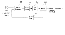
- FIG. 6 is a configuration block diagram of a general PLL circuit. As shown in FIG. 6, the PLL circuit compares an external reference signal (Fref) with a signal divided by 1 / N and outputs a phase difference signal (Phase Com).
- Fref external reference signal
- Phase Com phase difference signal
- VCXO voltage controlled crystal oscillator
- An output (internal reference signal) of the VCXO 35 is 1 /
- a divider 36 that divides the frequency into N is provided.
- the internal reference signal is an N ⁇ Fref signal.
- the PLL circuit synchronizes with the reference signal by applying feedback control to the internal VCXO 35 so that the phase difference between the reference signal input from the outside and the internal VCXO 35 becomes constant. The same oscillator output is obtained.
- the phase comparator 32 compares the phase of the highly stable external reference signal and the output signal from the VCXO 35 whose frequency is controlled by the input voltage, and the DC voltage obtained by smoothing the phase comparison result is fed back to the VCXO 35.
- the PLL circuit is widely used in communication and broadcasting apparatuses.
- Patent Document 1 JP-A-2000-083003
- Patent Document 2 JP-A-2003-179489
- a frequency counter performs a counting operation in synchronization with an output signal of a VCO (Voltage Controlled Oscillator) input within a time corresponding to a pulse width, and a count value corresponding to the oscillation frequency of the VCO is latched.
- VCO Voltage Controlled Oscillator
- a full-run frequency adjustment method is described in which, when the coefficient value is held in the circuit and the coefficient value is out of the predetermined range, the free-run frequency is adjusted to be within the predetermined range by changing the voltage applied to the VCO.
- the microcomputer counts the pulses of the output pulse signal of the VCO during a period in which the output of the phase comparator is at a predetermined level, and updates the control data according to the count value.
- a phase-locked loop circuit that automatically adjusts the free-running frequency of a voltage-controlled oscillator that combines the data with a signal from an LPF (Low Pass Filter) as an analog signal by a DAC (Digital Analog Converter) and uses it as a VCO frequency control signal Is described.
- JP 2000-083003 A Japanese Patent Laid-Open No. 2003-179489
- VC-TCXO temperature-compensated highly stable crystal oscillator
- a maximum frequency deviation of 10.5 ppm occurs after 10 years. If the carrier wave output frequency in communication is 800 MHz, a frequency deviation of 8.4 kHz occurs as in the case of the frequency deviation of the reference frequency. Such a frequency deviation is unacceptable as a system.
- Patent Documents 1 and 2 the output of the VCO is counted or the output of the phase comparator is counted to adjust the free-running frequency. It was not intended to make adjustments, and was not able to cope with aging.
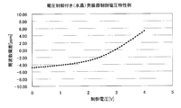
- FIG. 7 is a diagram illustrating an example of control voltage characteristics of a crystal oscillator with a voltage control function.
- the horizontal axis represents the control voltage
- the vertical axis represents the frequency deviation.
- the VCXO in the example of FIG. 7 can operate when the control voltage is 0 to 4V, but cannot operate when the control voltage is 4V or higher.
- FIG. 8 shows the characteristics in the case of VCXO free-run (free-running).
- FIG. 8 is a diagram showing the free-run characteristics of VCXO. Even in the case of VCXO, the frequency deviation increases with the passage of time, so that an appropriate control voltage changes. The same applies to a temperature-compensated crystal oscillator.
- FIG. 9 shows frequency characteristics when the external reference signal is a highly stable signal such as rubyium.
- FIG. 9 is a diagram illustrating frequency characteristics when the external reference signal is a highly stable signal. As shown in FIG. 9, when the external reference signal is a highly stable signal such as rubyium, it is within the range of the frequency deviation allowed by the system even if time elapses.
- FIG. 10 shows the frequency characteristics when the external reference signal is cut off.
- FIG. 10 is a diagram showing frequency characteristics when the external reference signal is cut off. As shown in FIG. 10, the frequency deviation when the external reference signal is cut off increases greatly at the time of disconnection, and then the frequency deviation gradually increases with time, and periodic calibration is performed. If not, the frequency range that the system can tolerate is exceeded.
- the present invention has been made in view of the above circumstances, corrects its own frequency, has no input of a highly stable reference signal, can maintain an oscillation frequency stably even when it is self-running, and from the outside It is an object of the present invention to provide an oscillation frequency control circuit that can oscillate with a control voltage in which the fixed voltage is variable.
- the present invention for solving the problems of the above-described conventional example includes, in an oscillation frequency control circuit, a voltage controlled oscillator, a frequency divider that divides an output from the voltage controlled oscillator, an external reference signal, and a frequency divider.
- Phase comparator that outputs phase difference and outputs phase difference signal
- loop filter that smoothes and outputs output from phase comparator
- detector circuit that detects external reference signal
- pulse generation information are input
- a pulse generation circuit that generates a pulse and outputs the pulse to the loop filter, a memory that stores information on the specified voltage and corresponding pulse generation, a control voltage variable circuit that performs adjustment to change the fixed voltage
- a selection switch that turns on / off the connection between the phase comparator and the loop filter, and turns on the selection switch if the level of the external reference signal detected by the detection circuit is within the appropriate range.
- the oscillation frequency control circuit has a control unit that outputs the above information to the pulse generation circuit.
- the present invention relates to a voltage controlled oscillator, a frequency divider that divides the output from the voltage controlled oscillator, an external reference signal, and a phase of the output from the frequency divider in the oscillation frequency control circuit.
- a phase comparator that outputs a signal
- a loop filter that smoothes and outputs the output from the phase comparator
- a detection circuit that detects an external reference signal
- a loop that generates a pulse when pulse generation information is input
- Pulse generation circuit that outputs to filter, memory that stores specified voltage information and corresponding pulse generation information, control voltage variable circuit that performs adjustment to change fixed voltage, and control that is input from control voltage variable circuit
- control signal for selecting a voltage is input, the control voltage is selected and output to the loop filter.
- the oscillation frequency control circuit includes a control unit that outputs the generated pulse generation information to the pulse generation circuit.
- the present invention compares the phase of the voltage control oscillator, the frequency divider that divides the output from the voltage control oscillator, the phase of the output from the external reference signal and the frequency divider, and the phase difference signal.
- a phase comparator that outputs a signal, a loop filter that smoothes and outputs the output from the phase comparator, a detection circuit that detects an external reference signal, and a pulse filter that generates pulses when information on pulse generation is input.
- a pulse generation circuit for outputting to the memory, a memory for storing prescribed voltage information and corresponding pulse generation information, a control voltage variable circuit for adjusting a fixed voltage, and a control voltage input from the control voltage variable circuit
- a control signal for selecting an external reference signal is input, the control voltage is selected and output to the loop filter.
- a phase comparator and a loop are selected.
- the control signal to select the pulse from the pulse generation circuit When the control signal to select the pulse from the pulse generation circuit is input when the connection to the filter is turned on, the selection switch that turns off the connection between the phase comparator and the loop filter, and the external reference signal detected by the detection circuit When the level is outside the proper range while the selection switch is turned on by outputting a control signal for selecting the external reference signal when the level is within the proper range, the control voltage variable circuit from the preset control voltage variable circuit
- the oscillation frequency control circuit includes a control unit that outputs either a control signal for selecting a control voltage or a control signal for selecting a pulse from the pulse generation circuit to a selection switch.
- the present invention is an oscillation frequency control circuit in which the control voltage variable circuit periodically calibrates and adjusts the fixed voltage and outputs the control voltage to the selection switch in the oscillation frequency control circuit.
- the present invention is an oscillation frequency control circuit in which the specified voltage information stored in the memory is a central control voltage in a control voltage capable of controlling the voltage controlled oscillator in the oscillation frequency control circuit.
- the oscillation frequency control circuit instead of storing the prescribed voltage information and the corresponding pulse generation information in the memory, an appropriate control voltage for the aging time and the corresponding pulse generation information are stored.
- the oscillation frequency control circuit is configured to search for a control voltage according to the above, read information on pulse generation corresponding to the searched control voltage, and output the information to the pulse generation circuit.
- the present invention provides a level detection circuit for detecting the voltage level of the output from the loop filter and outputting the latest voltage information to the control unit in the oscillation frequency control circuit.
- the latest voltage information, a plurality of voltage information and a voltage / pulse generation information table for storing information on pulse generation corresponding to the voltage information are stored, and the control unit is a level detection circuit
- the latest voltage information in the memory is updated with the latest voltage information input from the memory, and when the level of the external reference signal is outside the proper range, the latest voltage information is supported from the memory voltage / pulse generation information table.
- the oscillation frequency control circuit reads the information of pulse generation and outputs it to the pulse generation circuit.
- the present invention is an oscillation frequency control circuit using a crystal oscillator with a voltage control function, a temperature-compensated crystal oscillator, or a thermostat crystal oscillator with a voltage control function in place of the voltage control oscillator in the oscillation frequency control circuit.
- the pulse generation circuit is a pulse width modulation circuit
- the pulse generation information output from the control unit is an oscillation frequency control circuit whose information is pulse width modulation duty cycle information.
- the voltage-controlled oscillator the frequency divider that divides the output from the voltage-controlled oscillator, the phase comparison that outputs the phase difference signal by comparing the phase of the output from the external reference signal and the frequency divider Generator, a loop filter that smoothes and outputs the output from the phase comparator, a detection circuit that detects an external reference signal, and a pulse generator that generates a pulse when information on pulse generation is input and outputs it to the loop filter Selection to turn on / off connection of circuit, memory for storing specified voltage information and corresponding pulse generation information, control voltage variable circuit for adjustment to change fixed voltage, and phase comparator and loop filter If the level of the switch and the external reference signal detected by the detection circuit is within the proper range, the selection switch is turned on.
- a control unit that outputs an instruction to select the control voltage when selecting a control voltage from the path, and a pulse generation circuit that stores pulse generation information stored in the memory when the control voltage is not selected Because it is an oscillation frequency control circuit, it corrects its own frequency, does not have a highly stable reference signal input, and oscillates with a control voltage with a variable external fixed voltage when running, or pulse There is an effect that either one of keeping the oscillation frequency by the pulse from the generation circuit to be stable can be set.
- the voltage-controlled oscillator the frequency divider that divides the output from the voltage-controlled oscillator, the phase comparison that outputs the phase difference signal by comparing the phase of the output from the external reference signal and the frequency divider Generator, a loop filter that smoothes and outputs the output from the phase comparator, a detection circuit that detects an external reference signal, and a pulse generator that generates a pulse when information on pulse generation is input and outputs it to the loop filter
- a circuit a memory for storing prescribed voltage information and corresponding pulse generation information, a control voltage variable circuit for adjusting a fixed voltage, and a control signal for selecting a control voltage input from the control voltage variable circuit Is input, the control voltage is selected and output to the loop filter.
- the selection switch for turning on / off the connection between the phase comparator and the loop filter is selected.
- a control signal for preferentially selecting the control voltage is output to the selection switch, and the instruction is not input
- the selection switch is turned on. If the level is outside the proper range, the selection switch is turned off and the pulse generation information stored in the memory is pulsed.
- the voltage-controlled oscillator the frequency divider that divides the output from the voltage-controlled oscillator, the phase that outputs the phase difference signal by comparing the phase of the external reference signal and the output from the frequency divider
- a comparator a loop filter that smoothes and outputs the output from the phase comparator, a detection circuit that detects an external reference signal, and a pulse that generates a pulse and outputs it to the loop filter when pulse generation information is input
- a generation circuit a memory for storing prescribed voltage information and corresponding pulse generation information, a control voltage variable circuit for adjusting a fixed voltage, and a control for selecting a control voltage input from the control voltage variable circuit When the signal is input, the control voltage is selected and output to the loop filter.
- the connection between the phase comparator and the loop filter is turned on.
- the selection switch for turning off the connection between the phase comparator and the loop filter and the level of the external reference signal detected by the detection circuit are within an appropriate range.
- a control signal for selecting an external reference signal When a control signal for selecting an external reference signal is output and the selection switch is turned on, and the level is outside the proper range, a control signal for selecting a preset control voltage from the control voltage variable circuit or Since it is an oscillation frequency control circuit having a control unit that outputs any one of the control signals for selecting a pulse from the pulse generation circuit to the selection switch, the self-frequency is corrected, there is no input of a highly stable reference signal, When self-running, it oscillates in advance with a control voltage that makes the fixed voltage from outside variable, or the oscillation frequency by the pulse from the pulse generation circuit is reduced. There is an effect that can be set either to or kept at a.
- control voltage variable circuit is the oscillation frequency control circuit that periodically calibrates and adjusts the fixed voltage and outputs the control voltage to the selection switch, the voltage controlled oscillator is oscillated with a stable fixed voltage. There is an effect that can.
- the oscillation frequency control circuit uses the specified voltage information stored in the memory as the central control voltage in the control voltage that can control the voltage controlled oscillator, the self-frequency is corrected and the oscillation frequency Has an effect that can be kept stable.
- the memory instead of storing the prescribed voltage information and the corresponding pulse generation information, stores the appropriate control voltage with respect to the aging time and the corresponding pulse generation information.
- a characteristic table is stored, and the control unit has a timer inside to measure the time, and when the level of the external reference signal is outside the proper range, the control voltage corresponding to the time measured from the aging characteristic table of the memory Since the oscillation frequency control circuit reads the pulse generation information corresponding to the searched control voltage and outputs the information to the pulse generation circuit, the frequency correction can be adapted to the secular change.
- a level detection circuit that detects the voltage level of the output from the loop filter and outputs the latest voltage information to the control unit
- the memory includes prescribed voltage information and corresponding pulse generation information.
- a plurality of voltage information and a voltage / pulse generation information table for storing the corresponding pulse generation information
- the control unit receives the latest input from the level detection circuit.
- the latest voltage information of the memory is updated with the voltage information of the memory, and when the level of the external reference signal is out of the proper range, the pulse generation information corresponding to the latest voltage information is obtained from the memory voltage / pulse generation information table. Since the oscillation frequency control circuit reads and outputs to the pulse generation circuit, there is no input of the reference signal, and even if it is self-running, it will take over the previous state. There is an effect that can maintain the oscillation frequency stably.
- the oscillation frequency control circuit compares the phase of the output from the voltage controlled oscillator, the frequency divider that divides the output from the voltage controlled oscillator, the external reference signal and the frequency divider, A phase comparator that outputs a phase difference signal, a loop filter that smoothes and outputs the output from the phase comparator, a detection circuit that detects an external reference signal, and a pulse when information on pulse generation is input
- a pulse generation circuit that outputs to the loop filter, a memory that stores prescribed voltage information and corresponding pulse generation information, a control voltage variable circuit that performs adjustment to change the fixed voltage, and a control voltage variable circuit.
- control voltage When the control signal for selecting the control voltage is input, the control voltage is selected and output to the loop filter. When the control voltage is not selected, the phase comparator and the loop filter When a selection switch for turning on / off the connection and an instruction for selecting a control voltage from the control voltage variable circuit are input, a control signal for preferentially selecting the control voltage is output to the selection switch, and the instruction is input. If the level of the external reference signal detected by the detection circuit is within the proper range, the selection switch is turned on, and if the level is outside the proper range, the selection switch is turned off and stored in the memory.
- It has a control unit that outputs pulse generation information to the pulse generation circuit, corrects its own frequency, does not have a highly stable reference signal input, and can keep the oscillation frequency stable even when it runs independently Further, it can oscillate with a control voltage in which a fixed voltage from the outside is made variable.
- the oscillation frequency control circuit includes a voltage controlled oscillator, a frequency divider that divides the output from the voltage controlled oscillator, an external reference signal, and a phase of the output from the frequency divider.
- a phase comparator that compares and outputs a phase difference signal, a loop filter that smoothes and outputs the output from the phase comparator, a detection circuit that detects an external reference signal, and a pulse when information on pulse generation is input
- Generator for generating and outputting to a loop filter, memory for storing prescribed voltage information and corresponding pulse generation information, a control voltage variable circuit for adjusting a fixed voltage, and a control voltage variable circuit When a control signal for selecting a control voltage input from is input, the control voltage is selected and output to the loop filter.
- a phase comparison is performed.
- the selection switch that turns off the connection between the phase comparator and the loop filter and the external circuit detected by the detection circuit
- a control voltage variable circuit that is set in advance when the level goes out of the proper range while the selection switch is turned on by outputting a control signal for selecting the external reference signal when the level of the reference signal is within the proper range.
- the oscillation frequency control circuit has a control unit that outputs either a control signal for selecting a control voltage from the control signal or a control signal for selecting a pulse from the pulse generation circuit to the selection switch, the self-frequency is corrected, When there is no input of a highly stable reference signal and self-runs, it is made to oscillate with a control voltage in which a fixed voltage from the outside is made variable beforehand, or pulse generation There is an effect that can be set to either to keep stable the oscillation frequency by the pulse from the road.
- the oscillation frequency control circuit includes an aging characteristic table that stores an appropriate control voltage with respect to aging time and information on pulse generation corresponding to the aging time in the oscillation frequency control circuit.
- the control unit is equipped with an internal timer to measure time, and when the level of the external reference signal is outside the proper range, the control voltage corresponding to the measured time is retrieved from the aging characteristics table of the memory.
- the pulse generation information corresponding to the searched control voltage is read and output to the pulse generation circuit, and the frequency correction can be made to correspond to the secular change.
- the oscillation frequency control circuit includes a level detection circuit that detects the voltage level of the output from the loop filter and outputs the latest voltage information to the control unit in the oscillation frequency control circuit.
- the latest voltage information in the memory, a plurality of voltage information and a voltage / pulse generation information table for storing the corresponding pulse generation information are stored, and the control unit receives the latest voltage information input from the level detection circuit.
- the control unit receives the latest voltage information input from the level detection circuit.
- FIG. 1 is a block diagram showing the configuration of an oscillation frequency control circuit according to an embodiment of the present invention.
- the oscillation frequency control circuit (this circuit) according to the embodiment of the present invention includes a filter 11, a phase comparator 12, a selection switch 13, a loop filter 14, a voltage controlled oscillator 15, A frequency divider 16, a detection circuit 17, an amplifier 18, a CPU (Central Processing Unit) 20, a memory 21, a PWM (Pulse Width Modulation) circuit 22, a level detection circuit 23, an AD converter 24, An AD converter 25 and a control voltage variable circuit 26 are included.
- the filter 11 is a filter that limits the band of an external reference signal of 10 MHz, for example. Although not essential as a basic configuration, it functions to remove high-frequency components of the external reference signal.
- the phase comparator 12 compares the phase of the reference signal output from the filter 11 and the signal divided by the frequency divider 16 and outputs a phase difference signal. When the phase comparator 12 detects the synchronization (lock) by comparing the phases of the external reference signal and the divided signal, it outputs a lock detection signal to the CPU 20 and detects the asynchronous (unlock). Outputs an unlock detection signal to the CPU 20.
- the selection switch 13 is a fixed voltage mode (A) for supplying a fixed voltage from the control voltage variable circuit 26 to the loop filter 14 in response to a switching instruction (switching control signal) from the CPU 20, the phase comparator 12, the loop filter 14, and the like.
- the selection switch 13 receives a switching control signal for selecting one of the fixed voltage mode (A), the external reference signal mode (B), and the internal voltage mode (C) from the CPU 20.
- the CPU 20 normally outputs a switching control signal so as to enter the external reference signal mode (B), and outputs a switching control signal for selecting the internal voltage mode (C) in an abnormal state where the external reference signal is not input.
- the CPU 20 when an instruction for selecting the fixed voltage mode (A) is input from the input unit to the CPU 20, the CPU 20 outputs a switching control signal for preferentially selecting the fixed voltage mode (A). That is, the selection switch 13 operates in the external reference signal mode (B) unless the switching control signal for the fixed voltage mode (A) is input, and switches to the internal voltage mode (C) in an abnormal state. Yes.
- the loop filter 14 is a filter that smoothes the output voltage from the phase comparator 12. In other words, the loop filter 14 smoothes the control voltage input to the voltage controlled oscillator 15.
- the voltage controlled oscillator 15 oscillates and outputs a desired frequency (internal reference signal) by changing the frequency according to the control voltage from the loop filter 14.
- a crystal oscillator with voltage control (VCXO), VC-TCXO, a thermostat crystal oscillator with voltage control function (VC-OCXO), or the like may be used.
- the frequency divider 16 divides the internal reference signal output from the voltage controlled oscillator 15 by 1 / N.
- the detection circuit 17 performs level detection of the output signal from the filter 11.
- the amplifier 18 amplifies the signal detected by the detection circuit 17.
- the CPU 20 When an instruction for selecting the fixed voltage mode (A) is input from the input unit, the CPU 20 outputs a switching control signal for selecting the fixed voltage mode (A) to the selection switch 13, and the fixed voltage mode (A). If the selection instruction is not input from the input unit, when the normal state described below is determined, a switching control signal for selection of the external reference signal mode (B) is output, and further, the abnormal state described below When it is determined that, a switching control signal for selecting the internal voltage mode (C) is output.
- the CPU 20 inputs the control voltage information from the AD converter 25 and stores it in the memory 21 as the latest control voltage information. Specifically, the CPU 20 always receives the control voltage information from the AD converter 25, and does not update the memory 21 if there is no change from the previously input control voltage information. If there is a change, the CPU 20 displays the control voltage information in the memory 21. Update.
- the CPU 20 inputs the detected level of the external reference signal (external REF) from the AD converter 24, and receives an appropriate range (between the first threshold value and the second threshold value) stored in the memory 21. If it is within the proper range, an ON instruction (instruction to connect the phase comparator 12 and the loop filter 14) is output to the selection switch 13 and if it is out of the proper range For example, an OFF instruction (an instruction to disconnect the phase comparator 12 and the loop filter 14) is output to the selection switch 13.
- an ON instruction instruction to connect the phase comparator 12 and the loop filter 14
- an OFF instruction an instruction to disconnect the phase comparator 12 and the loop filter 14
- the CPU 20 refers to the voltage / PWM duty cycle table stored in the memory 21 and refers to the PWM duty cycle based on the voltage information of the current (latest) control voltage.
- the pulse width information according to the above is output to the PWM circuit 22.
- the memory 21 stores the latest control voltage information, the first threshold value and the second threshold value that are the reference of the appropriate range with respect to the detection level of the external REF, and the voltage / PWM duty cycle table. Yes.
- the control voltage information is detected by the level detection circuit 23, and when it is changed, it is updated in the memory 21 and held as the latest value.
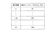
- FIG. 2 is a schematic diagram of a voltage / PWM duty cycle table. As shown in FIG. 2, the voltage / PWM duty cycle table stores a PWM duty cycle (%) for specifying a pulse width for voltage information.
- the voltage information is obtained by predetermining the PWM duty cycle of the pulse output from the PWM circuit 22 to the loop filter 14 in order to maintain the value of the control voltage from the loop filter 14 (control voltage information). It has become. Accordingly, when the PWM duty cycle corresponding to the control voltage information detected by the level detection circuit 23 is read from the voltage / PWM duty cycle table and the pulse corresponding to the cycle is output to the loop filter 14, the loop filter 14 The same control voltage as before is output to the voltage controlled oscillator 15.
- the PWM circuit 22 performs pulse width modulation on the PWM duty cycle data input from the CPU 20 and outputs a desired pulse signal to the loop filter 14. If voltage information data is output from the CPU 20, a DA (Digital / Analog) converter can be used instead of the PWM circuit.
- DA Digital / Analog
- the level detection circuit 23 detects the DC voltage output from the loop filter 14 and outputs it to the AD converter 25 as control voltage information.
- the AD converter 24 converts the detection level of the external REF output from the amplifier 18 from an analog signal to a digital signal and outputs it to the CPU 20.
- the AD converter 25 converts the control voltage information from the level detection circuit 23 from an analog signal to a digital signal and inputs it to the CPU 20.
- the input abnormality of the external reference signal can be recognized by the CPU 20 based on the detection level of the external REF output from the detection circuit 17 and the amplifier 18, and therefore the unlock detection signal from the phase comparator 12 is used. Not.
- the CPU 20 If the instruction for selecting the fixed voltage mode (A) is not input from the input unit, the CPU 20 outputs a switching control signal for selecting the external reference signal mode (B) to the selection switch 13 in the normal state, and the selection switch Reference numeral 13 denotes a state in which the phase comparator 12 and the loop filter 14 are connected.
- the phase comparator 12 outputs the signal of the phase difference between the external reference signal and the signal from the frequency divider 16 to the voltage controlled oscillator 15 via the loop filter 14 and controls the oscillation frequency in the voltage controlled oscillator 15. ing.
- the level detection circuit 23 detects the latest control voltage and outputs it to the CPU 20 via the AD converter 25.
- the CPU 20 updates the latest control voltage information in the memory 21 if the control voltage information is changed. To do.
- the external reference signal is detected by the detection circuit 17, amplified by the amplifier 18, the level of the external REF is detected, and is output to the CPU 20 via the AD converter 24.
- CPU 20 determines whether or not the input external REF detection level is within an appropriate range. Specifically, if there is a value of the detection level of the external REF between the first threshold value and the second threshold value indicating the appropriate range stored in the memory 21, it is determined that the value is within the appropriate range. If there is no external REF detection level value between the first threshold value and the second threshold value, it is determined that the value is outside the proper range.
- the CPU 20 maintains the selection switch 13 in the normal state and keeps the on state (external reference signal mode) in which the phase comparator 12 and the loop filter 14 are connected.
- the selection switch 13 is set to an abnormal state to turn off the phase comparator 12 and the loop filter 14 (internal voltage mode), and the phase comparator 12 and the loop filter 14 are disconnected.
- the CPU 20 reads the latest control voltage information stored in the memory 21, reads the PMW duty cycle corresponding to the voltage information from the voltage / PMW duty cycle table, and outputs a pulse that becomes the PWM duty cycle.
- Information (data) for formation is output to the PWM circuit 22.
- the PWM circuit 22 generates a pulse in accordance with the pulse formation information input from the CPU 20 and outputs a control voltage to the voltage controlled oscillator 15 via the loop filter 14.
- the CPU 20 when an abnormality occurs in the external reference signal, particularly when no external reference signal is input (in the case of self-running), the CPU 20 immediately detects the abnormality by the output from the detection circuit 17 and the amplifier 18. Then, the output of the phase comparator 12 is cut off, and a pulse similar to the control voltage that has been controlling the voltage controlled oscillator 15 so far is output from the PWM circuit 22. That is, by using the output from the PWM circuit 22 instead of the output of the phase comparator 12, it is possible to take over the previous state and optimize the frequency oscillation in the voltage controlled oscillator 15.
- both the base station from which the external reference signal can be obtained and the base station from which the external reference signal cannot be obtained can be handled by a single circuit. And in the case of a base station that can obtain an external reference signal, the self-frequency is corrected, there is no input of a highly stable reference signal, and the oscillation frequency can be kept stable even when it is self-running. It is possible to oscillate with a control voltage in which the fixed voltage from is variable.
- the CPU 20 preferentially selects the fixed voltage mode (A).
- the external reference signal mode (B) is selected in the normal state and becomes abnormal
- a control voltage in which a fixed voltage from outside is made variable in advance when self-running without correcting a self-stable reference signal is input. Can be set, or the oscillation frequency by the pulse from the pulse generation circuit can be kept stable.
- the pulse output from the PWM circuit 22 is generated based on the latest control voltage information detected by the level detection circuit 23.
- the default voltage information is stored, and the default voltage information is stored.
- Information on pulse generation may be output based on the PWM duty cycle corresponding to the voltage information.
- the memory 21 stores a center voltage value within an appropriate range, and the PWM duty cycle corresponding to the center voltage value is 50%. If the control voltage of 14 operates from 0 to 3.3V, the control voltage is set to 3.3 / 2V. Note that an arbitrary voltage value other than the center voltage value may be stored to set a corresponding control voltage. If the default voltage information is used, the components of the level detection circuit 23 and the AD converter 25 and the voltage / PMW duty cycle table in the memory 21 can be eliminated.
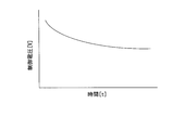
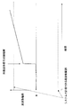
- FIG. 3 is a diagram showing characteristics at the time of calibration.
- the frequency deviation gradually increases or decreases as time elapses when no external reference signal is input.
- the figure shows a rise. Therefore, when an appropriate reference signal is input at a specific timing and then the input of the reference signal is stopped, the frequency deviation returns to the center frequency by self-running control, and calibration is performed.
- frequency control is performed using the center voltage value within the control range of the control voltage for the voltage controlled oscillator 15. According to this circuit, the calibration work can be performed without connecting a special circuit during calibration.
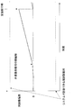
- FIG. 4 shows an example of optimum control voltage characteristics with respect to secular change in this circuit.
- FIG. 4 is a diagram showing aging / control voltage characteristics. As shown in FIG. 4, in this circuit, the optimum control voltage decreases with time (however, the case where the frequency deviation increases) is shown.
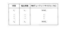
- FIG. 5 is a schematic diagram of an aging characteristic table.
- the memory 21 stores a voltage / PMW duty cycle table. Instead of this table, the aging characteristic table of FIG. 5 is used.
- the aging characteristic table of FIG. 5 further provides a time factor in the relationship between the voltage information and the PWM duty cycle. Specifically, voltage information appropriate for the passage of time is set, and a PWM duty cycle is set corresponding to the voltage information and stored as a table.
- the CPU 20 includes a timer inside and measures the passage of time.
- the CPU 20 when the detection level of the external reference signal is outside the proper range, the CPU 20 turns off the selection switch 13 and refers to the time measured by the internal timer, and corresponds to the time.
- the PWM duty cycle is searched from the voltage information to be output, information for generating a pulse according to the PWM duty cycle is output to the PWM circuit 22, and a desired pulse is generated by the PWM circuit 22 via the loop filter 14.
- a control voltage is output to the voltage controlled oscillator 15.
- the CPU 20 corrects the oscillation frequency by using the voltage information corresponding to the secular change when the external reference signal is abnormal and the pulse generated according to the PWM duty cycle corresponding thereto. There is an effect that the frequency control circuit can cope with the secular change.
- calibration may be performed in the circuit configuration according to the second embodiment.
- the CPU 20 measures the passage of time, and performs frequency control using a voltage value corresponding to the passage of time with reference to an aging characteristic table during calibration work. Thereby, there is an effect that the calibration work can be made to correspond to the secular change of the frequency control circuit.
- the present invention corrects its own frequency, does not have a highly stable reference signal input, can keep the oscillation frequency stable even when it is self-running, and oscillates with a control voltage with a variable fixed voltage from the outside. This is suitable for an oscillation frequency control circuit that can be used.
Landscapes
- Stabilization Of Oscillater, Synchronisation, Frequency Synthesizers (AREA)
Priority Applications (2)
| Application Number | Priority Date | Filing Date | Title |
|---|---|---|---|
| CN2008801227621A CN101911496B (zh) | 2007-12-25 | 2008-10-30 | 振荡频率控制电路 |
| US12/801,772 US7884657B2 (en) | 2007-12-25 | 2010-06-24 | Oscillation frequency control circuit |
Applications Claiming Priority (2)
| Application Number | Priority Date | Filing Date | Title |
|---|---|---|---|
| JP2007331767A JP4625494B2 (ja) | 2007-12-25 | 2007-12-25 | 発振周波数制御回路 |
| JP2007-331767 | 2007-12-25 |
Related Child Applications (1)
| Application Number | Title | Priority Date | Filing Date |
|---|---|---|---|
| US12/801,772 Continuation US7884657B2 (en) | 2007-12-25 | 2010-06-24 | Oscillation frequency control circuit |
Publications (1)
| Publication Number | Publication Date |
|---|---|
| WO2009081516A1 true WO2009081516A1 (ja) | 2009-07-02 |
Family
ID=40800835
Family Applications (1)
| Application Number | Title | Priority Date | Filing Date |
|---|---|---|---|
| PCT/JP2008/003108 Ceased WO2009081516A1 (ja) | 2007-12-25 | 2008-10-30 | 発振周波数制御回路 |
Country Status (4)
| Country | Link |
|---|---|
| US (1) | US7884657B2 (enExample) |
| JP (1) | JP4625494B2 (enExample) |
| CN (1) | CN101911496B (enExample) |
| WO (1) | WO2009081516A1 (enExample) |
Cited By (1)
| Publication number | Priority date | Publication date | Assignee | Title |
|---|---|---|---|---|
| JP2015528903A (ja) * | 2012-06-29 | 2015-10-01 | クゥアルコム・インコーポレイテッドQualcomm Incorporated | バックグラウンド水晶発振器較正 |
Families Citing this family (10)
| Publication number | Priority date | Publication date | Assignee | Title |
|---|---|---|---|---|
| JP4374463B2 (ja) * | 2006-12-26 | 2009-12-02 | 日本電波工業株式会社 | 発振周波数制御回路 |
| US8330644B2 (en) * | 2010-07-14 | 2012-12-11 | The United States Of America As Represented By The Administrator Of The National Aeronautics And Space Administration | Expandable and reconfigurable instrument node arrays |
| CN103312265B (zh) * | 2012-03-12 | 2017-07-04 | 飞思卡尔半导体公司 | 振荡器电路 |
| CN102798431B (zh) * | 2012-08-30 | 2014-04-09 | 北京京仪海福尔自动化仪表有限公司 | 一种压电晶体振荡及检测装置 |
| JP6172989B2 (ja) * | 2013-03-26 | 2017-08-02 | 日本電波工業株式会社 | 発振装置 |
| US9160159B2 (en) * | 2013-07-24 | 2015-10-13 | Stmicroelectronics S.R.L. | Circuit breaker and method of controlling a power transistor with a circuit breaker |
| JP2017194789A (ja) * | 2016-04-19 | 2017-10-26 | ローム株式会社 | クロック発生装置、電子回路、集積回路、及び電気機器 |
| CN106027041B (zh) * | 2016-05-12 | 2019-03-05 | 中国电子科技集团公司第四十一研究所 | 一种高性能自检测外参考时基电路及其实现方法 |
| US10778235B2 (en) * | 2018-10-28 | 2020-09-15 | Nuvoton Technology Corporation | Intermittent tuning of an oscillator |
| CN111490781B (zh) * | 2020-04-22 | 2023-05-26 | 中国科学院国家授时中心 | 一种基于温度变化差驾驭压控晶振的时间保持方法 |
Citations (5)
| Publication number | Priority date | Publication date | Assignee | Title |
|---|---|---|---|---|
| JPH01307317A (ja) * | 1988-06-06 | 1989-12-12 | Mitsubishi Electric Corp | Pll回路 |
| JPH0450935U (enExample) * | 1990-09-06 | 1992-04-28 | ||
| JPH04343524A (ja) * | 1991-05-20 | 1992-11-30 | Casio Comput Co Ltd | Pll回路 |
| JPH04369927A (ja) * | 1991-06-19 | 1992-12-22 | Hitachi Ltd | Pll発振器 |
| JP2006121171A (ja) * | 2004-10-19 | 2006-05-11 | Matsushita Electric Ind Co Ltd | 周波数補正機能付きクロック供給装置 |
Family Cites Families (21)
| Publication number | Priority date | Publication date | Assignee | Title |
|---|---|---|---|---|
| JPS60186115A (ja) * | 1984-03-06 | 1985-09-21 | Mitsubishi Electric Corp | 位相同期回路 |
| JP2644890B2 (ja) * | 1989-05-18 | 1997-08-25 | 三菱電機株式会社 | 位相同期回路 |
| JPH047911A (ja) * | 1990-04-25 | 1992-01-13 | Nec Corp | 位相同期発振回路 |
| JPH0450935A (ja) | 1990-06-15 | 1992-02-19 | Nikon Corp | カメラのバッテリチェック装置 |
| JPH0470010A (ja) * | 1990-07-09 | 1992-03-05 | Nec Eng Ltd | Plo回路 |
| JPH05243992A (ja) * | 1992-02-28 | 1993-09-21 | Sony Corp | Pll回路 |
| US6337589B1 (en) * | 1997-09-11 | 2002-01-08 | Mitsubishi Denki Kabushiki Kaisha | Phase-lock loop with independent phase and frequency adjustments |
| JP2000083003A (ja) | 1998-09-04 | 2000-03-21 | Tif:Kk | フリーラン周波数調整方式 |
| JP3367465B2 (ja) * | 1999-05-13 | 2003-01-14 | 日本電気株式会社 | 発振周波数調整装置 |
| JP3501778B2 (ja) * | 2001-05-30 | 2004-03-02 | 日本電気株式会社 | Pll回路 |
| JP3674850B2 (ja) | 2001-12-11 | 2005-07-27 | ソニー株式会社 | 電圧制御発振器の自走周波数の自動調整機能を有する位相ロックループ回路 |
| US6680874B1 (en) * | 2002-08-29 | 2004-01-20 | Micron Technology, Inc. | Delay lock loop circuit useful in a synchronous system and associated methods |
| JP2006005489A (ja) * | 2004-06-15 | 2006-01-05 | Sharp Corp | Pll回路および高周波受信装置 |
| EP1911160B1 (en) * | 2005-04-27 | 2013-05-29 | Semiconductor Energy Laboratory Co., Ltd. | Pll circuit and semiconductor device having the same |
| JP4459911B2 (ja) * | 2006-02-08 | 2010-04-28 | 富士通株式会社 | ホールドオーバ機能付きdpll回路 |
| US7805122B2 (en) * | 2006-08-29 | 2010-09-28 | Texas Instruments Incorporated | Local oscillator with non-harmonic ratio between oscillator and RF frequencies using digital mixing and weighting functions |
| US7564280B2 (en) * | 2006-11-30 | 2009-07-21 | Broadcom Corporation | Phase locked loop with small size and improved performance |
| US7804344B2 (en) * | 2007-04-20 | 2010-09-28 | Micron Technology, Inc. | Periodic signal synchronization apparatus, systems, and methods |
| CN101842986A (zh) * | 2007-11-02 | 2010-09-22 | 松下电器产业株式会社 | 扩频时钟产生装置 |
| US7800451B2 (en) * | 2008-08-20 | 2010-09-21 | Silicon Laboratories Inc. | Frequency adjustment for clock generator |
| US7733151B1 (en) * | 2008-12-08 | 2010-06-08 | Texas Instruments Incorporated | Operating clock generation system and method for audio applications |
-
2007
- 2007-12-25 JP JP2007331767A patent/JP4625494B2/ja active Active
-
2008
- 2008-10-30 CN CN2008801227621A patent/CN101911496B/zh active Active
- 2008-10-30 WO PCT/JP2008/003108 patent/WO2009081516A1/ja not_active Ceased
-
2010
- 2010-06-24 US US12/801,772 patent/US7884657B2/en active Active
Patent Citations (5)
| Publication number | Priority date | Publication date | Assignee | Title |
|---|---|---|---|---|
| JPH01307317A (ja) * | 1988-06-06 | 1989-12-12 | Mitsubishi Electric Corp | Pll回路 |
| JPH0450935U (enExample) * | 1990-09-06 | 1992-04-28 | ||
| JPH04343524A (ja) * | 1991-05-20 | 1992-11-30 | Casio Comput Co Ltd | Pll回路 |
| JPH04369927A (ja) * | 1991-06-19 | 1992-12-22 | Hitachi Ltd | Pll発振器 |
| JP2006121171A (ja) * | 2004-10-19 | 2006-05-11 | Matsushita Electric Ind Co Ltd | 周波数補正機能付きクロック供給装置 |
Cited By (4)
| Publication number | Priority date | Publication date | Assignee | Title |
|---|---|---|---|---|
| JP2015528903A (ja) * | 2012-06-29 | 2015-10-01 | クゥアルコム・インコーポレイテッドQualcomm Incorporated | バックグラウンド水晶発振器較正 |
| US10397887B2 (en) | 2012-06-29 | 2019-08-27 | Qualcomm Incorporated | Background crystal oscillator calibration |
| US10772053B2 (en) | 2012-06-29 | 2020-09-08 | Qualcomm Incorporated | Background crystal oscillator calibration |
| US11800464B2 (en) | 2012-06-29 | 2023-10-24 | Qualcomm Incorporated | Background oscillator calibration |
Also Published As
| Publication number | Publication date |
|---|---|
| JP2009159013A (ja) | 2009-07-16 |
| CN101911496A (zh) | 2010-12-08 |
| CN101911496B (zh) | 2013-02-20 |
| US20100264961A1 (en) | 2010-10-21 |
| JP4625494B2 (ja) | 2011-02-02 |
| US7884657B2 (en) | 2011-02-08 |
Similar Documents
| Publication | Publication Date | Title |
|---|---|---|
| JP4625494B2 (ja) | 発振周波数制御回路 | |
| KR101077730B1 (ko) | 발진 주파수 제어 회로 | |
| US7332979B2 (en) | Low noise reference oscillator with fast start-up | |
| JP4355350B2 (ja) | 発振周波数制御回路 | |
| US6664827B2 (en) | Direct digital synthesizer phase locked loop | |
| CN100483947C (zh) | 使用2-pi滑动检测粗调锁相环(pll)合成器的系统和方法 | |
| KR101515099B1 (ko) | 전하펌프, 전하펌프 보정 장치 및 이를 포함한 위상 동기 루프 | |
| JP2015082815A (ja) | 発振器 | |
| JP5145398B2 (ja) | 発振周波数制御回路 | |
| CN102195643A (zh) | Pll装置 | |
| KR100847799B1 (ko) | 위상 동기 루프 및 그 온도 보상 방법 | |
| JP2002151956A (ja) | 周波数校正機能付き圧電発振器 | |
| JP2004172686A (ja) | 基準信号発生器 | |
| WO2004013968A1 (ja) | デジタルvco及びそのデジタルvcoを用いたpll回路 | |
| US20250357937A1 (en) | Oscillation Circuit, Oscillation Control Method, Phase-Locked Loop Circuit, and Electronic Device | |
| JP2013074604A (ja) | 周波数シンセサイザ | |
| JP2000031819A (ja) | クロック同期回路 | |
| JP2011040850A (ja) | 周波数シンセサイザ | |
| JPH1065528A (ja) | Pll回路 |
Legal Events
| Date | Code | Title | Description |
|---|---|---|---|
| WWE | Wipo information: entry into national phase |
Ref document number: 200880122762.1 Country of ref document: CN |
|
| 121 | Ep: the epo has been informed by wipo that ep was designated in this application |
Ref document number: 08864970 Country of ref document: EP Kind code of ref document: A1 |
|
| NENP | Non-entry into the national phase |
Ref country code: DE |
|
| 122 | Ep: pct application non-entry in european phase |
Ref document number: 08864970 Country of ref document: EP Kind code of ref document: A1 |