WO2005116774A1 - パターン形成方法 - Google Patents
パターン形成方法 Download PDFInfo
- Publication number
- WO2005116774A1 WO2005116774A1 PCT/JP2005/009554 JP2005009554W WO2005116774A1 WO 2005116774 A1 WO2005116774 A1 WO 2005116774A1 JP 2005009554 W JP2005009554 W JP 2005009554W WO 2005116774 A1 WO2005116774 A1 WO 2005116774A1
- Authority
- WO
- WIPO (PCT)
- Prior art keywords
- light
- pattern
- photosensitive layer
- pattern forming
- meth
- Prior art date
- Legal status (The legal status is an assumption and is not a legal conclusion. Google has not performed a legal analysis and makes no representation as to the accuracy of the status listed.)
- Ceased
Links
Classifications
-
- G—PHYSICS
- G03—PHOTOGRAPHY; CINEMATOGRAPHY; ANALOGOUS TECHNIQUES USING WAVES OTHER THAN OPTICAL WAVES; ELECTROGRAPHY; HOLOGRAPHY
- G03F—PHOTOMECHANICAL PRODUCTION OF TEXTURED OR PATTERNED SURFACES, e.g. FOR PRINTING, FOR PROCESSING OF SEMICONDUCTOR DEVICES; MATERIALS THEREFOR; ORIGINALS THEREFOR; APPARATUS SPECIALLY ADAPTED THEREFOR
- G03F7/00—Photomechanical, e.g. photolithographic, production of textured or patterned surfaces, e.g. printing surfaces; Materials therefor, e.g. comprising photoresists; Apparatus specially adapted therefor
- G03F7/70—Microphotolithographic exposure; Apparatus therefor
- G03F7/70216—Mask projection systems
- G03F7/70283—Mask effects on the imaging process
- G03F7/70291—Addressable masks, e.g. spatial light modulators [SLMs], digital micro-mirror devices [DMDs] or liquid crystal display [LCD] patterning devices
-
- G—PHYSICS
- G03—PHOTOGRAPHY; CINEMATOGRAPHY; ANALOGOUS TECHNIQUES USING WAVES OTHER THAN OPTICAL WAVES; ELECTROGRAPHY; HOLOGRAPHY
- G03F—PHOTOMECHANICAL PRODUCTION OF TEXTURED OR PATTERNED SURFACES, e.g. FOR PRINTING, FOR PROCESSING OF SEMICONDUCTOR DEVICES; MATERIALS THEREFOR; ORIGINALS THEREFOR; APPARATUS SPECIALLY ADAPTED THEREFOR
- G03F7/00—Photomechanical, e.g. photolithographic, production of textured or patterned surfaces, e.g. printing surfaces; Materials therefor, e.g. comprising photoresists; Apparatus specially adapted therefor
- G03F7/70—Microphotolithographic exposure; Apparatus therefor
- G03F7/70216—Mask projection systems
- G03F7/70275—Multiple projection paths, e.g. array of projection systems, microlens projection systems or tandem projection systems
-
- G—PHYSICS
- G02—OPTICS
- G02B—OPTICAL ELEMENTS, SYSTEMS OR APPARATUS
- G02B26/00—Optical devices or arrangements for the control of light using movable or deformable optical elements
- G02B26/08—Optical devices or arrangements for the control of light using movable or deformable optical elements for controlling the direction of light
- G02B26/0816—Optical devices or arrangements for the control of light using movable or deformable optical elements for controlling the direction of light by means of one or more reflecting elements
- G02B26/0833—Optical devices or arrangements for the control of light using movable or deformable optical elements for controlling the direction of light by means of one or more reflecting elements the reflecting element being a micromechanical device, e.g. a MEMS mirror, DMD
-
- H—ELECTRICITY
- H05—ELECTRIC TECHNIQUES NOT OTHERWISE PROVIDED FOR
- H05K—PRINTED CIRCUITS; CASINGS OR CONSTRUCTIONAL DETAILS OF ELECTRIC APPARATUS; MANUFACTURE OF ASSEMBLAGES OF ELECTRICAL COMPONENTS
- H05K3/00—Apparatus or processes for manufacturing printed circuits
- H05K3/0073—Masks not provided for in groups H05K3/02 - H05K3/46, e.g. for photomechanical production of patterned surfaces
- H05K3/0082—Masks not provided for in groups H05K3/02 - H05K3/46, e.g. for photomechanical production of patterned surfaces characterised by the exposure method of radiation-sensitive masks
Definitions
- the present invention relates to a pattern forming method in which light modulated by a light modulation means such as a spatial light modulation element is imaged on a pattern forming material, and the pattern forming material is exposed.
- a light modulation means such as a spatial light modulation element
- An exposure apparatus which passes light modulated by a spatial light modulation element or the like through an imaging optical system, forms an image of the light on a predetermined pattern forming material, and exposes the pattern forming material.
- the exposure apparatus basically comprises a spatial light modulation element in which a large number of picture elements, each of which modulates the emitted light in accordance with a control signal, are arranged in a two-dimensional manner, and the spatial light modulation element And an imaging optical system for forming an image by light modulated by the spatial light modulation element on a pattern forming material (see Non-Patent Document 1 and Patent Document 1). ).
- the spatial light modulator examples include a liquid crystal display (LCD), a digital micro mirror device (DMD), and the like, and the DMD functions as the pixel unit to reflect light in accordance with a control signal.
- LCD liquid crystal display
- DMD digital micro mirror device
- the image forming optical system is an image forming optical system.
- the system is used.
- the luminous flux of each picture element in the spatial light modulation element is magnified and projected if it is projected.
- the size of the picture becomes large and the sharpness of the picture is lowered.
- a first imaging optical system is disposed in the optical path of the light modulated by the spatial light modulation element, and the first image formation is performed.
- a micro lens array in which micro lenses corresponding to the respective picture elements of the spatial light modulation element are arranged in an array is disposed, and in the optical path of the light passing through the micro lens array.
- a second imaging optical system for imaging a modulated light image on a pattern forming material or a screen, and to magnify and project the image by these first and second imaging optical systems. It has been proposed.
- the size of the image projected onto the pattern forming material and the screen is enlarged, while the light from each pixel of the spatial light modulator is collected by each microlens of the microlens array. Therefore, the image size (spot size) in the projected image is narrowed and kept small, so that the image sharpness can be kept high.
- an exposure apparatus has been proposed in which a DMD is used as the spatial light modulation element and the DMD and a microlens array are combined (see Patent Document 2).
- an aperture plate having an aperture corresponding to each microlens of the microlens array is disposed on the rear side of the microlens array, and the lens passes through the corresponding microphone lens.
- An exposure apparatus has been proposed in which only light passes through the opening (see Patent Document 3). In these cases, the extinction ratio can be increased by preventing the light from the adjacent micro lenses not corresponding to the apertures of the aperture plate from being incident thereon.
- the tent film for protecting the holes is the uncured region of the photosensitive layer.
- the substrate is broken in the process of dissolving and removing the metal and the process of etching the exposed metal layer portion.
- Patent Document 1 Japanese Patent Application Laid-Open No. 2004-1244
- Patent Document 2 Japanese Patent Application Laid-Open No. 2001-305663
- Patent Document 3 Japanese Patent Application Publication No. 2001-500628
- Non-Patent Document 1 Akito Ishikawa "Development shortening and mass production application by maskless exposure”, “Electronics mounting technology”, Technical Research Association, Inc., Vol. 18, No. 6, 2002, p. 74- 79 Disclosure of the Invention
- permanent patterns such as wiring patterns can be formed with high precision and efficiency by suppressing distortion of an image formed on a pattern forming material having at least a photosensitive layer,
- the purpose is to provide a pattern formation method that is highly compatible with tentness and resolution.
- ⁇ 1> After laminating the photosensitive layer in the pattern-forming material having at least a photosensitive layer on a substrate to be treated, light is exposed to light having different amounts of energy with respect to two or more arbitrary regions of the photosensitive layer.
- the thickness is not uniform, and the photosensitive layer of the pattern forming material can be uniformly cured, and etching defects and the like caused by thickness unevenness can be avoided.
- Energy of the irradiated light, saying the "exposure amount” can be replaced, the unit is (m) jZcm 2.
- the light from the light irradiating means is modulated by the light modulating means having n pixels for exposing and receiving light from the light irradiating means, and then the light emitting surface of the light dot is formed.
- the light irradiation unit is Light is emitted toward the light modulation means.
- the n picture elements in the light irradiator receive and emit the light from the light irradiator, thereby modulating the light received from the light irradiator.
- the light modulated by the light modulation means passes through the aspheric surface of the microlens array, thereby correcting aberration due to distortion of the exit surface of the picture element and distortion of the image formed on the pattern forming material. Is suppressed.
- the exposure to the pattern forming material is performed with high definition. For example, a high definition pattern is then formed by developing the photosensitive layer.
- the light from the light irradiating means is modulated by the light modulating means having n picture elements for receiving and emitting the light from the light irradiating means, and then the light is emitted from the peripheral portion of the picture element.
- the pattern formation method according to 1) above wherein exposure is performed through a microlens array in which microlenses having an opening shape of a negative lens are arranged.
- the light irradiation unit irradiates light toward the light modulation unit.
- the n picture elements in the light irradiator receive and emit the light from the light irradiator, thereby modulating the light received from the light irradiator.
- the light modulated by the light modulation means is modulated by the light modulation means.
- the light power from the peripheral portion of the picture element in the microlens array is not incident.
- the distortion is caused by passing through a microlens having a lens opening shape.
- the light reflected at the periphery of the large picture element, in particular at the four corners, is not collected, and distortion of the collected light can be prevented.
- the exposure to the pattern forming material is performed with high definition. For example, thereafter, the photosensitive layer is developed to form a high definition pattern.
- the pattern forming method according to ⁇ 3> having an aspheric surface capable of correcting an aberration due to distortion of an exit surface in a picture element portion.
- the light modulated by the light modulation means passes through the aspheric surface of the micro lens array, whereby the aberration due to the distortion of the exit surface of the pixel portion is generated.
- the distortion of the image which is corrected and formed on the patterning material is suppressed.
- the exposure to the pattern forming material is performed with high definition. For example, a high-definition pattern is formed by subsequently developing the photosensitive layer.
- ⁇ 5> The surface according to any one of ⁇ 2> to ⁇ 4>, wherein the aspheric surface is a toric surface. It is a turn formation method.
- the aspheric surface is a toric surface, whereby the aberration due to the distortion of the radiation surface in the picture portion is efficiently corrected, and an image is formed on the pattern formation material. Image distortion is efficiently suppressed.
- the exposure to the pattern forming material is performed with high definition. For example, a high-definition pattern is then formed by developing the photosensitive layer.
- ⁇ 6> The pattern forming method according to ⁇ 3> to ⁇ 5>, wherein the microlens has a circular lens opening shape.
- ⁇ 7> The pattern forming method according to any one of ⁇ 3> to ⁇ 6>, wherein the lens opening shape is defined by providing a light shielding portion on the lens surface.
- the substrate to be treated has a hole, and the energy amount of light irradiated to the photosensitive layer on the hole above the hole and the photosensitive layer other than the photosensitive layer on the hole are irradiated. It is the pattern formation method according to any one of ⁇ 1> to ⁇ 7> different from the amount of energy of light.
- the energy amount of light irradiated to the photosensitive layer on the hole portion the energy amount of light irradiated to the photosensitive layer other than the photosensitive layer on the hole portion; Because of the difference, after development after exposure, a cured film having a hardness different from that on other regions or a cured film having a different thickness is formed on the hole portion.
- the light modulation means may be any n non-sequentially arranged out of n picture elements.
- the pattern forming method according to any one of ⁇ 2> to ⁇ 9>, wherein the full picture portion can be controlled according to pattern information.
- any of less than n pixels sequentially arranged from among the n pixels in the light modulation means may be selected according to the pattern information. By controlling, the light from the light irradiating means is modulated at high speed.
- ⁇ 12> The pattern forming method according to ⁇ 11>, wherein the spatial light modulator is a digital 'micro mirror' device (DMD).
- DMD digital 'micro mirror' device
- ⁇ 13> The pattern forming method according to any one of ⁇ 1> to ⁇ 12>, wherein the exposure is performed through the aperture array.
- the extinction ratio is improved by performing exposure through the aperture array.
- exposure is performed with extremely high definition. For example, then, by developing the photosensitive layer, a very high-definition pattern is formed.
- ⁇ 14> The pattern forming method according to any one of ⁇ 1> to ⁇ 13>, wherein the exposure is performed while relatively moving the exposure light and the photosensitive layer.
- exposure is carried out at high speed by performing exposure while relatively moving the modulated light and the photosensitive layer.
- ⁇ 15> The pattern forming method according to any one of ⁇ 1> to ⁇ 14>, wherein the photosensitive layer is developed after the exposure.
- ≪ 17 The pattern forming method according to < 16 >, wherein the permanent pattern is a wiring pattern, and the formation of the permanent pattern is performed by at least one of etching and plating.
- the permanent pattern force is the wiring pattern, and the formation of the permanent pattern is performed by at least one of an etching process and a plating process, thereby achieving high definition.
- Wiring pattern is formed.
- ⁇ 18> The pattern forming method according to any one of ⁇ 2> to ⁇ 17>, wherein the light irradiation unit can combine and emit two or more lights.
- exposure is performed with exposure light having a deep depth of focus because the light irradiation means can combine and irradiate two or more lights.
- exposure to the pattern forming material is performed with extremely high definition. For example, after that, by developing the photosensitive layer, a very high-definition pattern is formed.
- a collective optical system in which a light irradiation means condenses a plurality of lasers, a multimode optical fiber, and a plurality of laser beams respectively irradiated and coupled to the multimode optical fiber It is a method for forming a pattern according to any one of the above ⁇ 2> to ⁇ 18>.
- the light irradiation unit condenses the laser beams respectively irradiated by the plurality of laser powers by the collective optical system and enables coupling to the multimode optical fiber.
- the exposure is performed with the deep exposure light.
- exposure to the pattern forming material is performed with extremely high definition. For example, by developing the photosensitive layer thereafter, a very high-definition pattern is formed.
- ⁇ 20> The pattern forming method according to any one of ⁇ 1> to ⁇ 19>, wherein the photosensitive layer is formed by transfer of a dry film resist.
- ⁇ 21> The pattern forming method according to any one of ⁇ 1> to ⁇ 20>, wherein the photosensitive layer is formed by application of a liquid resist.
- ⁇ 22> The pattern forming method according to any one of ⁇ 1> to ⁇ 21>, wherein the photosensitive layer contains at least a dye, a polymerizable compound, and a photopolymerization initiator.
- Binder force The pattern forming method according to ⁇ 22>, which has an acidic group.
- ⁇ 24> The pattern forming method according to any one of ⁇ 22> to ⁇ 23>, wherein the binder is a boule copolymer.
- the polymerizable compound has at least one of a urethane group and an aryl group 22.
- a photopolymerization initiator is a halogenated hydrocarbon derivative, hexaarylbiimidazole, oxime derivative, organic peroxide, thio compound, ketone compound, aromatic salt, meta opening
- ⁇ 29> The pattern forming method according to ⁇ 1>, wherein the thickness of the photosensitive layer is 1 to 100, and the range from ⁇ 1> to ⁇ 28>.
- ⁇ 33> The method for forming a pattern according to any one of ⁇ 30> to ⁇ 32>, wherein the support is long.
- Pattern Forming Material Force The pattern forming method according to any one of ⁇ 1> to ⁇ 33>, which is elongated and wound in a roll.
- ⁇ 35> The pattern forming method according to any one of ⁇ 1> to ⁇ 34>, wherein the protective film is formed on the photosensitive layer in the pattern forming material.
- Figure 1 is an example of a partially enlarged view showing the configuration of a digital micromirror device (DMD).
- DMD digital micromirror device
- FIG. 2A is an example of an explanatory diagram for explaining the operation of the DMD.
- FIG. 2B is an example of an explanatory diagram for explaining the operation of the DMD similar to FIG. 2A.
- FIG. 3A is an example of a plan view showing the arrangement of exposure beams and scanning lines in comparison with the case where the DMD is not inclined and the case where the DMD is inclined.
- FIG. 3B is an example of a plan view showing the arrangement of exposure beams and scanning lines in comparison with the case where the DMDs are not inclined and arranged as in FIG. 3A.
- FIG. 4A is an example of a diagram showing an example of the usage area of DMD.
- FIG. 4B is an example of a diagram showing an example of the usage area of DMD similar to FIG. 4A.
- FIG. 5 is an example of a plan view for explaining an exposure method of exposing a pattern forming material by one scan by a scanner.
- FIG. 6A is an example of a plan view for explaining an exposure method of exposing a pattern forming material by a plurality of scans by a scanner.
- FIG. 6B is an example of a plan view for explaining an exposure method in which a pattern forming material is exposed by a plurality of scans by the same scanner as in FIG. 6A.
- FIG. 7 is an example of a schematic perspective view showing the appearance of an example of a pattern forming apparatus.
- FIG. 8 is an example of a schematic perspective view showing the configuration of a scanner of the pattern forming apparatus.
- FIG. 9A is an example of a plan view showing an exposed area formed on a patterning material.
- FIG. 9B is an example of a diagram showing the arrangement of exposure areas by each exposure head.
- FIG. 10 is an example of a perspective view showing a schematic configuration of an exposure head including a light modulation means.
- FIG. 11 is an example of a cross-sectional view in the sub scanning direction along the optical axis showing the configuration of the exposure head shown in FIG.
- Figure 12 is an example of a controller that controls DMD based on pattern information.
- FIG. 13A is an example of a cross-sectional view along the optical axis showing the configuration of another exposure head having a different combination optical system.
- FIG. 13B is an example of a plan view showing a light image projected on the surface to be exposed in the case where a microlens array or the like is not used.
- FIG. 13C is an example of a plan view showing a light image projected on the surface to be exposed when a microlens array or the like is used.
- FIG. 14 is an example of a diagram showing distortion of a reflection surface of a micro mirror constituting a DMD by contour lines.
- FIG. 15A is an example of a graph showing distortion of the reflection surface of the micro mirror as two diagonal directions of the mirror.
- FIG. 15B is an example of a graph showing distortion of the reflection surface of the micro mirror similar to FIG. 15A with respect to two diagonal directions of the mirror.
- FIG. 16A is an example of a front view of a microlens array used in a patterning device.
- FIG. 16B is an example of a side view of a microlens array used in a patterning device.
- FIG. 17A is an example of a front view of microlenses constituting a microlens array.
- FIG. 17B is an example of a side view of a microlens forming the microlens array.
- FIG. 18A is an example of a schematic view showing a state of light collection by a microlens in one cross section.
- FIG. 18B is an example of a schematic view showing a state of focusing by a microlens in one cross-sectional view 18A and in another cross-section.
- FIG. 19A is an example of a diagram showing the results of simulation of the beam diameter in the vicinity of the focusing position of the microlens of the present invention.
- FIG. 19B is an example of a diagram showing simulation results similar to FIG. 19A with respect to different positions.
- FIG. 19C shows simulation results similar to Figs. 19A and 19B in different positions! , FIG.
- FIG. 19D is an example of a diagram showing simulation results similar to those in FIGS. 19A to 19C at another position V.
- FIG. 20A is an example of a diagram showing a result of simulating a beam diameter in the vicinity of a focusing position of a microlens in a conventional pattern formation method.
- FIG. 20B is an example of a diagram showing simulation results similar to FIG. 20A with respect to different positions.
- FIG. 20C shows simulation results similar to Figs. 20A and 20B in different positions! , FIG.
- FIG. 20D is an example of a diagram showing simulation results similar to those of FIG. 20A to FIG. 20C at another position V.
- FIG. 21 is an example of a plan view showing another configuration of the combined laser light source.
- FIG. 22A is an example of a front view of microlenses constituting a microlens array.
- FIG. 22B is an example of a side view of a microlens forming the microlens array.
- FIG. 23A is an example of a schematic view showing a state of light collection by the microlenses of FIGS. 22A and 22B for an example in one cross section.
- FIG. 23B is an example of a schematic view showing the condensing state by the microlenses of FIGS. 22A and 22B in one cross section and in another cross section of an example of 23A.
- FIG. 24A is an example of an explanatory view of a concept of correction by the light quantity distribution correction optical system.
- FIG. 24B is an example of an explanatory diagram of a concept of correction by the light quantity distribution correction optical system similar to FIG. 24A.
- FIG. 24C is an example of an explanatory diagram of a concept of correction by the light amount distribution correction optical system similar to FIG. 24A and FIG. 24B.
- FIG. 25 is an example of a graph showing the light quantity distribution when the light irradiation means has a Gaussian distribution and the light quantity distribution is not corrected.
- FIG. 26 is an example of a graph showing the light quantity distribution after correction by the light quantity distribution correction optical system.
- FIG. 27A is a perspective view showing the configuration of a fiber array light source.
- FIG. 27B is an example of a front view showing the arrangement of light emitting points in the laser emission part of the fiber array light source.
- FIG. 28 is an example of a diagram showing the configuration of a multimode optical fiber.
- FIG. 29 is an example of a plan view showing the configuration of a combined laser light source.
- FIG. 30 is an example of a plan view showing the configuration of a laser module.
- FIG. 31 is an example of a side view showing the configuration of the laser module shown in FIG.
- FIG. 32 is a partial side view showing the configuration of the laser module shown in FIG.
- FIG. 33 is an example of a perspective view showing the configuration of a laser array.
- FIG. 34A is an example of a perspective view showing the configuration of a multi-cavity laser.
- FIG. 34B is an example of a perspective view of a multi-cavity laser array in which the multi-cavity lasers shown in FIG. 38A are arranged in an array.
- FIG. 35 is an example of a plan view showing another configuration of the combined laser light source.
- FIG. 36A is an example of a plan view showing another configuration of the multiplexing laser light source.
- FIG. 36B is an example of a cross-sectional view along the optical axis of FIG. 36A.
- FIG. 37A shows the depth of focus in the conventional exposure apparatus and the pattern formation method of the present invention.
- FIG. 10 is an example of a cross-sectional view along the optical axis showing the difference from the depth of focus due to (pattern formation device).
- FIG. 37B is an example of a cross-sectional view along the optical axis showing the difference between the depth of focus in the conventional exposure apparatus similar to FIG. 37A and the depth of focus by the pattern formation method (pattern formation device) of the present invention. It is.
- FIG. 38A is a front view showing another example of the microlens array that configures the macro array.
- FIG. 38B is a side view showing another example of the microlens array constituting the macro array.
- FIG. 39A is an example of a front view of a microlens array constituting a macro array.
- FIG. 39B is an example of a side view of a microlens array constituting a macro array.
- FIG. 40 is a graph showing an example of the shape of a spherical lens.
- FIG. 41 is a graph showing another example of lens surface shape.
- FIG. 42 is a perspective view showing another example of the microlens array.
- FIG. 43 is a plan view showing another example of the microlens array.
- FIG. 44 is a plan view showing another example of the microlens array.
- FIG. 45A is a longitudinal sectional view showing another example of the microlens array.
- FIG. 45B is a longitudinal sectional view showing another example of the microlens array similar to FIG. 45A.
- FIG. 45C is a longitudinal sectional view showing another example of the micro lens array similar to FIG. 45A and FIG. 45B.
- the pattern forming method of the present invention at least includes an exposure step for a laminate obtained by laminating the photosensitive layer of a pattern forming material having at least a photosensitive layer on a substrate, and includes other appropriately selected steps.
- the exposure step after laminating the photosensitive layer of the pattern forming material having at least a photosensitive layer on a substrate to be treated, n pixels for receiving and emitting light from the light irradiating means to the photosensitive layer A microlens array in which microlenses having an aspheric surface capable of correcting an aberration due to distortion of an exit surface of the drawing portion are modulated after the light from the light emitting unit is modulated by a light modulation unit having the microlens array, or In this step, exposure is carried out through a microlens array in which microlenses having lens opening shapes are arrayed without entering light from the peripheral portion of the drawing portion, and it is a step for arbitrary two or more regions of the photosensitive layer. Light of different energy levels.
- the method of changing the amount of energy of light to be applied to the arbitrary region may be appropriately selected according to the purpose of the restriction.
- the method of adjusting the total amount of energy supplied by controlling the irradiation time of light the method of adjusting the intensity of irradiation light by controlling the amount of current supplied to the light source, and the turning on and off of the light source
- the exposure apparatus controls the first and second light sources, the scanning unit for scanning the light from the light source, and the on / off control of the light source independently.
- a first area and a second area of the substrate by a function of calculating the position to turn on / off the first and second light sources based on the information of the area where the exposure light quantity is to be changed.
- different regions on the substrate are exposed with different exposure amounts by exposing with both light sources and exposing the other regions with only one light source.
- the amount of energy of the light to be irradiated can be arbitrarily selected according to the thickness and hardness required for the cured layer to be formed.
- the amount of light energy to be irradiated for forming a tent film covering the hole is determined on the basis of the optimum energy for forming a hardened layer on the wiring. 1. It is preferable to set 1 to 10 times.
- the area where the exposure amount is to be changed can be appropriately selected according to the purpose without particular limitation.
- the wiring portion is not affected, and the diameter of the hole portion is 1 ⁇ m to 100 mm in the range. Areas of large diameter may be exposed.
- the light modulation means as long as it has n drawing parts, it can be appropriately selected according to the purpose of being not particularly limited.
- a spatial light modulation element and the like are suitably mentioned.
- the spatial light modulation device include digital micro mirror devices (DMD), MEMS (Micro Electro Mechanical Systems) type spatial light modulation devices (S LM; Special Light Modulator), and modulation of transmitted light by an electro-optical effect Optical elements (PLZT elements), liquid crystal light shirts (FLC), etc., and among them, DMD is suitably mentioned.
- DMD digital micro mirror devices
- MEMS Micro Electro Mechanical Systems
- S LM Micro Electro Mechanical Systems
- PZT elements electro-optical effect Optical elements
- FLC liquid crystal light shirts
- the DMD 50 has a large number (for example, 1024 ⁇ 768) of micro mirrors (micro mirrors) 62, each of which constitutes a pixel (pixel) on the SRAM cell (memory cell) 60. It is a mirror device arranged in a shape. In each pixel, a micro mirror 62 supported by a support is provided at the top, and a material with high reflectance such as aluminum is vapor-deposited on the surface of the micro mirror 62. The reflectance of the micro mirror 62 is 90% or more, and the arrangement pitch thereof is 13. as an example in the vertical direction and the horizontal direction. Also, immediately under the micro mirror 62, a silicon gate CMOS SRAM cell 60 manufactured on a typical semiconductor memory manufacturing line is disposed via a pillar including a hinge and a yoke, and the whole is monolithically configured. ing.
- the microphone mirror 62 supported by the support has ⁇ degrees (for example, ⁇ 12 degrees) with respect to the substrate side on which the DMD 50 is disposed about the diagonal. It is tilted in the range of).
- FIG. 2A shows a state in which the micro mirror 62 is in the on state and inclined to + ⁇ degrees
- FIG. 2A shows a state in which the micro mirror 62 is in the off state and is inclined to ⁇ degrees. Therefore, by controlling the tilt of the micro mirror 62 at each pixel of the DMD 50 as shown in FIG. 1 according to the pattern information, the laser light ⁇ input to the DMD 50 is directed to the tilt direction of each micro mirror 62 To be reflected.
- FIG. 1 shows an example of a state in which a part of the DMD 50 is enlarged and the micro mirror 62 is controlled to + ⁇ degree or ⁇ degree.
- the on / off control of each micro mirror 62 is performed by the controller 302 connected to the DMD 50.
- a light absorber (not shown) is disposed in the direction in which the laser beam reflected by the microphone mirror 62 in the off state travels.
- the DMD 50 is preferably arranged to be slightly inclined so that the short side thereof forms a predetermined angle ⁇ (for example, 0.1 ° to 5 °) with the sub-scanning direction.
- Fig. 3 shows the scanning locus of the reflected light image (exposure beam) 53 by each micro mirror when the DMD 50 is not inclined, and Fig. 3 shows the scanning locus of the exposure beam 53 when the DMD 50 is inclined. .
- a micro mirror array force in which a large number (for example, 1024) of micro mirrors are arranged in the longitudinal direction.
- a force with a large number of ⁇ 1_ for example, 756 threads arranged in the lateral direction.
- the scan width W when the DMD 50 is inclined and the inclination of the DMD 50 are not inclined.
- the scan width w in the case is approximately the same.
- high-speed modulation a method for increasing the modulation speed in the light modulation means (hereinafter referred to as “high-speed modulation”) will be described.
- the light modulation means can control any of less than n pixels continuously arranged among the n pixels according to pattern information. Since the data processing speed of the light modulation means is limited, and the modulation speed per line is determined in proportion to the number of pixels used, any number less than n pixels arranged continuously will be determined. Using only increases the modulation speed per line.
- the laser beam B When the laser beam B is irradiated from the fiber array light source 66 to the DMD 50, the laser beam reflected when the microphone mirror of the DMD 50 is on is imaged on the pattern forming material 150 by the lens system 54, 58. . In this manner, the laser light emitted from the fiber array light source 66 is turned on and off for each picture element, and the pattern forming material 150 is exposed with approximately the same number of picture elements (exposure area 168) as the number of drawing elements used for the DMD 50. Ru. In addition, the patterning material 150 is moved at a constant speed with the stage 152, whereby the patterning material 150 is sub-scanned by the scanner 162 in the direction opposite to the stage movement direction. Region 170 is formed.
- control is performed by the controller 302 so as to drive only a part of micro mirror rows (for example, 1024 ⁇ 256 rows).
- the micro mirror array disposed at the end of DMD 50 may be used as shown in FIG. 4B. May be used. Also, if some micro mirrors have defects, they will Depending on the situation, the micro mirror row used may be changed as appropriate, such as using a non-micro mirror row.
- the data processing speed of DMD 50 is limited, and the modulation speed per line is determined in proportion to the number of pixels used.
- the modulation speed of the hit is faster.
- the exposure method in which the exposure head is moved relative to the exposure surface continuously it is not necessary to use all the picture elements in the sub-scanning direction.
- the stage 152 follows the guide 158 by the stage driving device 304. It returns to the origin on the most upstream side of the gate 160, and is again moved along the guide 158 from the upstream side to the downstream side of the gate 160 at a constant speed.
- modulation can be performed twice as fast per line as compared with the case where all 768 sets are used.
- modulation can be performed three times faster per line as compared with the case where all 768 pairs are used.
- the micro mirror row force in which 1,024 micro mirrors are arranged in the main scanning direction and the D MD arranged in 768 threads in the sub scanning direction
- the modulation speed per line becomes faster than in the case of driving all micro mirror rows.
- control signal described in the example of partially driving the micromirror of the DMD on the substrate whose length in the direction corresponding to the predetermined direction is longer than the length in the direction intersecting the predetermined direction Accordingly, even when using a long and thin DMD in which a large number of micromirrors capable of changing the angle of the reflecting surface are arranged in a two-dimensional manner, the number of micromirrors for controlling the angle of the reflecting surface decreases. You can be fast.
- the method of the exposure it is preferable to carry out while relatively moving the exposure light and the photosensitive layer. In this case, it is preferable to use in combination with the high speed modulation. Thereby, high-speed exposure can be performed in a short time.
- a single scan in the X direction by the scanner 162 forms a pattern.
- the patterning material 150 is scanned in the X direction by the scanner 162, and then the scanner 162 is moved by one step in the Y direction. The scanning and movement may be repeated so that scanning is performed in the direction, and the entire surface of the patterning material 150 may be exposed in a plurality of scans.
- the scanner 162 is provided with 18 exposure heads 166.
- the exposure head at least includes the light irradiation means and the light modulation means.
- the exposure is performed on a part of the area of the photosensitive layer to cure the part of the area, and in the development step described later, uncured regions other than the part of the hardened part are cured.
- the areas are removed and a pattern is formed.
- the pattern forming apparatus including the light modulation means includes a flat plate-like stage 152 for adsorbing and holding a sheet-like pattern forming material 150 on the surface.
- the stage 152 On the upper surface of a thick plate-like mounting table 156 supported by four legs 154, two guides 158 extending along the stage moving direction are installed.
- the stage 152 is disposed so that its longitudinal direction is in the stage moving direction, and is supported by the guide 158 so as to be capable of reciprocating.
- the pattern forming apparatus has a driving device (not shown) for driving the stage 152 along the guide 158.
- a U-shaped gate 160 is provided in the central portion of the installation table 156 so as to straddle the moving path of the stage 152. Each of the ends of the U-shaped gate 160 is fixed to both sides of the mounting table 156.
- a scanner 162 is provided on one side of the gate 160, and a plurality of (for example, two) detection sensors 164 for detecting the front end and the rear end of the pattern forming material 150 are provided on the other side. There is.
- the scanner 162 and the detection sensor 164 are respectively attached to the gate 160 and fixedly disposed above the movement path of the stage 152.
- the scanner 162 and the detection sensor 164 are connected to a controller (not shown) that controls them.
- the scanner 162 has a plurality (for example, 14) of exposure heads 166 arranged in a matrix of m rows and n columns (for example, 3 rows and 5 columns). Have. In this example In the third row, four exposure heads 166 are arranged in relation to the width of the patterning material 150. The individual exposure heads arranged in the m-th row and the n-th column are denoted as exposure head 166.
- An exposure area 168 by the exposure head 166 has a rectangular shape whose short side is in the sub-scanning direction.
- strip-shaped exposed areas 170 are formed in the patterning material 150 for each of the exposure heads 166.
- the exposure area 168 is indicated, the exposure area 168
- each of the exposure heads of each row arranged in a line is arranged such that the strip-shaped exposed regions 170 are arranged without gaps in the direction perpendicular to the sub scanning direction. In the arrangement direction, they are arranged with a predetermined interval (a natural number multiple of the long side of the exposure area, double in this example). Therefore, exposure between the exposure area 168 of the first row and the exposure area 168 can be performed.
- the non-exposed area is exposed by the exposure area 168 of the second line and the exposure area 168 of the third line.
- Each of the exposure heads 166 to 166 is, as shown in FIG. 10 and FIG.
- a light modulation means spatial light modulation element which modulates each picture according to pattern information
- a digital 'micro mirror one' device As a light modulation means (spatial light modulation element which modulates each picture according to pattern information), a digital 'micro mirror one' device
- the DMD 50 is provided.
- the DMD 50 is connected to a later-described controller 302 (see FIG. 12) including a data processing unit and a mirror drive control unit.
- the data processing unit of the controller 302 generates a control signal for driving and controlling each micro mirror in the area to be controlled of the DMD 50 for each of the exposure heads 166 based on the input pattern information. The areas to be controlled will be described later.
- the mirror drive control unit controls the angle of the reflection surface of each micro mirror of the DMD 50 for each of the exposure heads 166 based on the control signal generated by the pattern information processing unit. The control of the angle of the reflecting surface will be described later.
- a fiber array light source provided with a laser emission portion in which emission end portions (light emitting points) of optical fibers are arranged in a line along a direction corresponding to the long side direction of the exposure area 168.
- a lens system 67 for correcting the laser beam emitted from the fiber array light source 66 and collecting it on the DMD, and a mirror 69 for reflecting the laser beam transmitted through the lens system 67 toward the DMD 50 are arranged in this order .
- the lens system 67 is schematically shown. It is
- the lens system 67 includes a condenser lens 71 for condensing the laser light B as illumination light emitted from the fiber array light source 66 and an optical path of the light passing through the condenser lens 71.
- a rod-shaped optical integrator (hereinafter referred to as “rod integrator”) 72 inserted and an imaging lens 74 disposed on the front side of the rod integrator 72, that is, on the side of the mirror 69 are also configured.
- the condenser lens 71, the rod integrator 72, and the imaging lens 74 cause the laser light emitted from the fiber array light source 66 to be incident on the DMD 50 as a light beam which is close to parallel light and whose intensity in the beam cross section is uniform.
- the shape and action of the rod integrator 72 will be described in detail later.
- the laser beam B emitted from the lens system 67 is reflected by the mirror 69 and irradiated to the DMD 50 through the TIR (total reflection) prism 70.
- this TIR prism 70 is omitted.
- an imaging optical system 51 for imaging the laser light B reflected by the DMD 50 on the pattern forming material 150 is disposed on the light reflection side of the DMD 50.
- this imaging optical system 51 is schematically shown in FIG. 10, as shown in detail in FIG. 11, the first imaging optical system consisting of the lens systems 52 and 54 and the lens systems 57 and 58 are used. And a microlens array 55 inserted between the two imaging optical systems, and an aperture array 59 and a force.
- the microlens array 55 is formed by arranging a large number of microlenses 55 a corresponding to each pixel of the DMD 50 in a two-dimensional manner. In this example, only 1024 X 256 of the 102 4 X 768 micro mirrors of the DMD 50 are driven as described later, and therefore, 1024 X 256 micro lenses 55a are arranged correspondingly. .
- the arrangement pitch of the micro lens 55a is 41 ⁇ m in both the longitudinal direction and the transverse direction.
- this microlens 55a has a focal length of 0.19 mm, an NA (numerical aperture) of 0.11, and is made of optical glass BK7. The shape of the microlens 55a will be described in detail later.
- the beam diameter of the laser beam B at the position of each of the microlenses 55a is 41 ⁇ m.
- the aperture array 59 is paired with each microlens 55 a of the microlens array 55. A corresponding large number of apertures (openings) 59a are formed.
- the diameter of the aperture 59a is, for example, 10 m.
- the first imaging optical system magnifies the image by the DMD 50 three times and forms an image on the microlens array 55.
- the second imaging optical system magnifies the image having passed through the microlens array 55 by 1.6 times, and forms and projects the image on the patterning material 150.
- the image by the DMD 50 will be magnified and projected on the patterning material 150 with a magnification of 4.8.
- a prism pair 73 is disposed between the second imaging optical system and the pattern forming material 150, and the pattern forming material 150 is moved by moving the prism pair 73 in the vertical direction in FIG. It is possible to adjust the focus of the image above.
- the pattern forming material 150 is sub-scan fed in the arrow F direction.
- the picture element may be suitably selected according to the purpose of being not particularly limited as long as it can receive and emit the light from the light irradiating means.
- the pattern of the present invention may be used.
- the pattern formed by the forming method is an image pattern, it is a pixel, and when the light modulation means includes a DMD, it is a micro mirror.
- the number (n) of the picture elements of the light modulation element can be appropriately selected according to the purpose of breaking the restriction.
- the arrangement of the picture elements in the light modulation element can be appropriately selected according to the purpose of being not particularly limited. For example, it is preferable to arrange in a two-dimensional lattice. , Is more preferred.
- An example is a force obtained by arraying microlenses having a lens aperture shape that does not allow light of peripheral force of the picture portion to be incident.
- the aspheric surface can be appropriately selected depending on the purpose without particular limitation.
- a toric surface is preferable.
- the microlens array, the aperture array, the imaging optical system, and the like will be described with reference to the drawings.
- FIG. 13A shows DMD 50, light irradiation means 144 for irradiating laser light to DMD 50, and lens systems (imaging optical systems) 454, 458, and DM D 50 for forming an image by magnifying the laser light reflected by DMD 50.
- a microlens array 472 in which a large number of microlenses 474 are arranged corresponding to each pixel, an aperture array 476 in which a large number of apertures 4 78 are provided corresponding to each microlens of the microlens array 472,
- the exposure head comprised with the lens system (imaging optical system) 480, 482 which images the laser beam which passed to the to-be-exposed surface 56 is shown.
- FIG. 1 the lens system
- FIG. 14 shows the result of measuring the flatness of the reflection surface of the micro mirror 62 constituting the DMD 50.
- FIG. In the figure, the same height position of the reflecting surface is shown connected by contour lines, and the pitch of the contour lines is 5 nm.
- the X direction and the y direction shown in the figure are the two diagonal directions of the micro mirror 62, and the micro mirror 62 rotates as described above about the rotation axis extending in the y direction.
- FIGS. 15A and 15B respectively show the height position displacement of the reflecting surface of the micro mirror 62 along the X direction and the y direction.
- FIG. 15A and FIG. 15B distortion is present on the reflective surface of the micro mirror 62, and when focusing on the central part of the mirror in particular, one diagonal direction (y direction) The distortion of 1S is larger than that of another diagonal direction (X direction). For this reason, there may occur a problem that the shape at the focusing position of the laser light B focused by the microlens 55 a of the microlens array 55 is distorted.
- the microlenses 55a of the micro lens array 55 have a special shape different from the conventional one. This point will be described in detail below.
- FIGS. 16A and 16B respectively show in detail the front shape and the side shape of the entire microlens array 55.
- the 1024 ⁇ 256 micromirrors 62 of the DMD 50 are driven, and the microlens array is correspondingly made.
- the 55 is configured by arranging 256 rows of microlenses 55a arranged in a row in the horizontal direction. .
- the arrangement order of the microlens array 55 is indicated by j in the horizontal direction, and by k in the vertical direction.
- FIGS. 17A and 17B respectively show the front shape and the side shape of one microphone lens 55 a in the microlens array 55.
- contour lines of the microphone lens 55a are also shown.
- the end face on the light emission side of each of the micro-lenses 55a has an aspheric shape that corrects the aberration due to the distortion of the reflection surface of the micro mirror 62.
- the condensed states of the laser light B in the cross section parallel to the X direction and the y direction are as schematically shown in FIGS. 18A and 18B, respectively. That is, comparing the cross section parallel to the X direction with the cross section parallel to the y direction, the radius of curvature of the micro lens 55a is smaller in the latter cross section, and the focal length is shorter. ing.
- the value of z in each of the drawings indicates the evaluation position of the focusing direction of the microlens 55a by the distance from the beam exit surface of the microlens 55a.
- the surface shape of the microlens 55 a used for the simulation is calculated by the following formula.
- X is the lens optical axis in the X direction O force means a distance
- Y means the distance of the lens optical axis O force in the y direction.
- the microlenses 55a are parallel to the focal length direction in a cross section parallel to the y direction.
- the pattern-forming material 150 it is possible to expose the pattern-forming material 150 to a distortion-free and more precise image. Further, in the present embodiment shown in FIGS. 19A to 19D, it can be understood that the region where the beam diameter is smaller is wider, that is, the focal depth is larger.
- the focal length in the cross section parallel to the X direction is parallel to the y direction. If the microlens is made of a toric lens smaller than the focal length in the cross section, it is possible to expose the image without any distortion on the pattern forming material 150 in the same manner.
- the aperture array 59 disposed in the vicinity of the light collection position of the microlens array 55 is disposed such that only light passing through the corresponding microlens 55 a is incident on each of the apertures 59 a. . That is, by providing the aperture array 59, the light from the adjacent microlens 55a which does not correspond to each aperture 59a is prevented from being incident, and the extinction ratio is enhanced.
- the effect of suppressing distortion of the beam shape at the focusing position of the microlens 55a can also be obtained. If this is done, the amount of light blocked by the aperture array 59 will be larger, and the light utilization efficiency will be reduced. On the other hand, in the case where the micro lens 55a has an aspherical shape, the light utilization efficiency is also kept high because the light is not blocked.
- a micro lens 55a which is a toric lens having different X direction and y direction curvatures which optically correspond to two diagonal directions of the micro mirror 62 is applied.
- the distortion of the micro mirror 62 as shown in Fig. 38A and Fig. 38 B, respectively, with frontal shape and contour shape with contour lines, two sides of the rectangular micro mirror 62 have optical directions corresponding to XX direction and yy Micro-lenses 55a 'may be applied which are made of toric lenses having different directional curvatures.
- the microlens 55 a may have a second-order aspheric shape or a higher-order (fourth-order, sixth-order aspheric shape).
- the beam shape can be further enhanced by adopting the above-mentioned high-order aspheric shape, and further, depending on the distortion of the reflection surface of the micro mirror 62, the X direction and y mentioned above can be obtained. It is also possible to adopt a lens shape in which the curvatures of the directions coincide with each other, and an example of such a lens shape will be described in detail below.
- the microlenses 55a "having front and side contours with contour lines in FIGS. 39A and 39B have equal curvatures in the X direction and y direction, respectively, and the curvatures are the curvature Cy of the spherical lens. Is corrected according to the distance h from the center of the lens. That is, the spherical lens shape that is the basis of the lens shape of this microphone lens 55a ′ ′ is, for example, a lens according to the following formula (Equation 2) The height (position of the lens curved surface in the optical axis direction) z is specified.
- Equation 3 the meaning of z is the same as the above equation (Equation 2), and here, the curvature Cy is calculated using the fourth order coefficient a and the sixth order coefficient b. It is correcting.
- the end face on the light emission side of the microlens 55 a is aspheric.
- a microlens array including one of the two light passing end surfaces as a spherical surface and the other as a cylindrical surface constitutes a microlens array as in the above embodiment. You can also get various effects.
- the micro lens 55a of the micro lens array 55 has an aspheric shape that corrects the aberration due to the distortion of the reflection surface of the micro mirror 62. Similar effects can be obtained even if each micro lens forming the micro lens array is provided with a refractive index distribution for correcting an aberration due to distortion of the reflection surface of the micro mirror 62 instead of adopting the spherical shape. .
- FIGS. 22A and 22B An example of such a microlens 155a is shown in FIGS. 22A and 22B.
- FIGS. 22A and 22B respectively show the front shape and the side shape of the micro lens 155a, and as shown in the figure, the external shape of the micro lens 155a is a parallel flat plate. The x and y directions in the figure are as described above.
- FIGS. 23A and 23B schematically show a state of focusing of the laser beam B in a cross section parallel to the x direction and the y direction by the microlens 155 a.
- the micro lens 155a has a refractive index distribution in which the optical axis O force also gradually increases outward, and the broken line shown in the micro lens 155a in the figure has a predetermined refractive index from the optical axis O. It shows the position changed with equal pitch.
- the rate of change in refractive index of the microlens 155a is larger in the latter cross section, and the focal length is It is getting shorter. Even when using a microlens array composed of such a refractive index distribution type lens, it is possible to obtain the same effect as the case of using the microlens array 55.
- the refractive index distribution as described above is added to the microlens whose surface shape is aspheric as in the case of the microlens 55a shown in FIGS. 17A, 17B, 18A and 18B previously.
- the aberration due to the distortion of the reflecting surface of the micro mirror 62 may be corrected by both the surface shape and the refractive index distribution.
- the micro lens array of this example is formed by arranging micro lenses having an opening lens shape which does not allow light from the peripheral portion of the picture element to enter.
- strain is present on the reflective surface of the micro mirror 62 of the DMD 50.
- the amount of strain variation is from the center of the micro mirror 62 It tends to become larger gradually as it goes to the periphery. And the above-mentioned tendency which becomes larger compared with the peripheral distortion change of one diagonal direction (y direction) of the micro mirror 62 is also more remarkable than the peripheral distortion change of another diagonal direction (X direction). There is.
- the microlens array of this example is applied to address the above-mentioned problems.
- the microlenses 255a arranged in an array form have a circular lens opening. Therefore, as described above, the laser light B reflected at the peripheral portion of the reflecting surface of the microphone mirror 62 with large distortion, particularly at the four corners, is not collected by the micro lens 255a, and the collected laser light B is collected. It is possible to prevent the shape at the position from being distorted. Therefore, it is possible to expose a distortion-free, higher-definition image on the pattern forming material 150.
- the back surface of the transparent member 255b (which is usually formed integrally with the micro lens 255a) holding the micro lens 255a. That is, the light shielding mask 255c is formed on the surface opposite to the surface on which the microlens 255a is formed, with the outer regions of the lens openings of the plurality of microlenses 255a separated from each other being filled. .
- the laser beam B reflected at the peripheral portion of the reflection surface of the micro mirror 62, particularly at the four corners, is absorbed and blocked there, so that the condensed laser beam B is The problem that the shape is distorted is reliably prevented.
- the aperture shape of the microlens is not limited to the above-mentioned circular shape.
- the micro-lens formed by arranging a plurality of microlenses 455a having elliptical apertures side by side as shown in FIG. It is also possible to apply a lens array 455 or a microphone lens array 555 in which a plurality of microlenses 555a each having a polygonal (rectangular in the illustrated example) opening as shown in FIG.
- the micro lenses 455a and 555a are formed by cutting a part of a conventional axisymmetric spherical lens into a circle or a polygon and have the same light collecting function as a conventional axisymmetric spherical lens.
- FIG. 45A, FIG. 45B and FIG. 45C it is also possible to apply a microlens array as shown in FIG. 45A, FIG. 45B and FIG. 45C.
- the surface of the transparent member 655 b on which the laser beam B is emitted A plurality of microlenses 655a similar to the above-mentioned mask 255c are formed in parallel so that a plurality of microlenses 655a similar to that of FIG. While the mask 255c in FIG. 42 is formed on the outer side of the lens opening, the mask 655c is provided in the lens opening.
- a plurality of microlenses 755 a are juxtaposed apart from each other on the surface of the transparent member 455 b from which the laser light B is emitted.
- a mask 755 c is interposed between the micro lenses 755 a. Is formed.
- a plurality of microlenses 855a are juxtaposed so as to be in contact with each other on the surface of the transparent member 855b from which the laser light B is emitted.
- the mask 855c is formed on the
- the masks 655 c, 755 c and 855 c all have circular openings as in the case of the mask 255 c described above, whereby the openings of the microlenses are defined to be circular.
- a configuration is provided such that a lens is opened so that light from the peripheral portion of the micro mirror 62 of the DMD 50 is not made incident by providing a mask or the like as in the microlenses 255a, 455a, 555a, 655a and 755a described above. 17A and 17B, the aspheric lens for correcting the aberration due to the distortion of the surface of the micro mirror 62 like the already described microlens 55a, and the microlens 155a shown in FIGS. 22A and 22B. It is also possible to adopt it together with a lens having a refractive index distribution for correcting the above-mentioned aberration. By doing so, the effect of preventing distortion of the exposed image due to distortion of the reflecting surface of the micro mirror 62 is synergistically enhanced.
- the micro lens 855 a has the aspherical shape and the refractive index distribution as described above.
- the imaging position force of the first imaging optical system such as the lens systems 52 and 54 shown in FIG. 11 is set on the lens surface of the microlens 855a, for example.
- the light utilization efficiency is increased, and the pattern forming material 150 can be exposed to light of higher intensity. That is, in this case, the first imaging optical system refracts light such that stray light due to distortion of the reflection surface of the micro mirror 62 converges at one point at the imaging position of the optical system. If the mask 855c is formed on the Light from the outside is not blocked and the light utilization efficiency is improved.
- the pattern of the present invention using a spatial light modulation element other than DMD when distortion is present on the surface of the picture element of the spatial light modulation element, the present invention is applied to correct the aberration due to the distortion and to prevent generation of distortion in the beam shape. is there.
- the cross-sectional area of the light beam reflected in the on direction by the DMD 50 is several times (eg, twice) by the lens system 454, 458. It is expanded.
- the expanded laser light is collected corresponding to each pixel of the DMD 50 by each microlens of the microlens array 472 and passes through the corresponding aperture of the aperture array 476.
- the laser beam having passed through the aperture is imaged on the surface 56 to be exposed by the lens systems 480 and 482.
- the laser light reflected by the DMD 50 is magnified several times by the magnifying lenses 454, 45 8 and projected onto the exposed surface 56, so that the entire image area becomes wider. .
- the microlens array 472 and the aperture array 476 are not disposed, as shown in FIG. 13B, one pixel size (spot size) of each beam spot BS projected onto the exposed surface 56 is the exposure area. It becomes large according to the size of 468, and the MTF (Modulation Transfer Function) characteristic representing the sharpness of exposure area 468 decreases.
- MTF Modulation Transfer Function
- the laser light reflected by the DMD 50 corresponds to each picture portion of the DMD 50 by each microlens of the microlens array 472. It is collected.
- the spot size of each beam spot BS can be reduced to a desired size (for example, lO ⁇ mX lO ⁇ m). It is possible to perform high-definition exposure while preventing the deterioration of characteristics.
- the exposure area 468 is inclined because the DMD 50 is inclined and disposed in order to eliminate the space between the pixels.
- the aperture array The beam can be shaped so that the spot size on the exposed surface 56 becomes a constant size, and adjacent to each other by passing through the aperture array provided corresponding to each pixel. Cross talk between lines can be prevented.
- the angle of the light beam incident on each of the microlenses of the microlens array 472 from the lens 458 is reduced. It is possible to prevent part of the luminous flux from being incident. That is, a high extinction ratio can be realized.
- the pattern forming method of the present invention may be used in combination with other optical systems appropriately selected from known optical systems, for example, a light intensity distribution correcting optical system comprising a pair of combination lenses.
- the light quantity distribution correction optical system changes the light beam width at each light emission position so that the ratio of the light beam width at the peripheral portion to the light beam width at the central portion near the optical axis becomes smaller at the light emission side than at the light incident side.
- the parallel luminous flux from the light irradiating means is irradiated to the DMD, the light quantity distribution on the surface to be irradiated is corrected so as to be substantially uniform.
- the light quantity distribution correcting optical system will be described below with reference to the drawings.
- FIG. 24A the case where the total luminous flux width (total luminous flux width) HO and HI of the incident luminous flux and the outgoing luminous flux are the same will be described.
- portions denoted by reference numerals 51 and 52 virtually represent the incident surface and the exit surface of the light quantity distribution correcting optical system.
- the light quantity distribution correction optical system enlarges the light beam width hO for the light beam having the same light beam width hO, hi on the incident side, and the light beam width hO for the central light beam, and conversely, to the incident light beam in the peripheral region. It acts to reduce its luminous flux width hi. That is, for the width hlo of the outgoing light flux at the central part and the width hll l of the outgoing light flux at the peripheral part, h1l ⁇ h1O.
- the luminous flux width By changing the luminous flux width in this way, it is possible to utilize the luminous flux of the central part, which usually has a large light quantity distribution, to the peripheral part where the light quantity is insufficient, and the light gain as a whole.
- the distribution of light quantity on the surface to be irradiated is made substantially uniform without reducing the efficiency of use.
- the degree of uniformity is, for example, within 30%, preferably within 20%, of the light quantity unevenness in the effective area.
- FIG. 24B shows the case where the entire luminous flux width H0 on the incident side is emitted by "reducing" to the width H2 (H0
- the light quantity distribution correction optical system has the same light beam width h0 and hi at the incident side, and the light beam width hlo at the central portion becomes larger at the output side than in the peripheral portion, On the contrary, the luminous flux width hi 1 at the periphery is made smaller than at the center.
- the reduction rate of light flux the reduction rate for the incident light flux at the central portion is smaller than that at the peripheral portion, and the reduction rate for the incident light flux at the peripheral portion is larger than that at the central portion.
- FIG. 24C shows the case where the entire luminous flux width H0 on the incident side is emitted by “expanding” to the width H3 (H0 and H3).
- the light quantity distribution correction optical system has the same light beam width h0 and hi at the incident side, and the light beam width hlo at the central portion becomes larger at the output side than in the peripheral portion, On the contrary, the luminous flux width hi 1 at the periphery is made smaller than at the center.
- the magnification of the light flux the magnification of the central part with respect to the incident luminous flux is made larger than that of the peripheral part, and the magnification of the peripheral part with respect to the incident luminous flux is made smaller than that of the central part.
- the light quantity distribution correcting optical system changes the luminous flux width at each emission position, and the ratio of the luminous flux width of the peripheral part to the luminous flux width of the central part near the optical axis Z1 is outputted as compared with the incident side. Since the light emission side is made smaller, the light having the same light beam width at the incident side is larger at the light emission side than at the peripheral portion at the central portion, and the light beam width at the peripheral portion is It becomes smaller than the central part. As a result, the light flux in the central portion can be utilized to the peripheral portion, and a substantially uniform light flux cross-section can be formed without reducing the light utilization efficiency of the entire optical system.
- lens data is shown in the case where the light quantity distribution at the cross section of the emitted light beam is Gaussian, as in the case where the light irradiation means is a laser array light source.
- the light quantity distribution of the light beam emitted from the light Fino becomes a Gaussian distribution.
- Such a case can also be applied to the pattern formation method of the present invention. Also, it can be applied to the case where the light quantity at the central part is larger than the light quantity at the peripheral part! By reducing the core diameter of the multimode optical fiber and approaching the configuration of the single mode optical fiber. It is.
- a pair of combination lenses is composed of two rotationally symmetric aspheric lenses. Assuming that the surface on the light incident side of the first lens disposed on the light incident side is the first surface, and the surface on the light emission side is the second surface, the first surface has an aspheric shape. When the surface on the light incident side of the second lens disposed on the light emission side is the third surface and the surface on the light emission side is the fourth surface, the fourth surface has an aspheric shape.
- curvature radius ri indicates the curvature radius of the i-th surface
- surface distance di indicates spacing on the optical axis between the i-th surface and the i + 1-th surface
- the unit of surface separation di value is millimeter (mm).
- the refractive index Ni indicates the value of the refractive index for the wavelength 405 nm of the optical element having the i-th surface.
- Table 2 below shows the aspheric surface data of the first and fourth surfaces.
- the aspheric surface data described above are represented by coefficients in the following formula (A) representing an aspheric surface shape.
- E indicates that the subsequent numerical value is an exponent that has a base of 10
- the numerical power represented by an exponential function based on the base 10 Indicates that the previous value of E "is to be multiplied. For example, “1. OE—02” indicates “1. 0 X 10 _2 ”.
- FIG. 26 shows the light quantity distribution of the illumination light obtained by the pair of combination lenses shown in Table 1 and Table 2.
- the horizontal axis indicates the coordinates from the optical axis, and the vertical axis indicates the light quantity ratio (%).
- FIG. 25 shows the light quantity distribution (Gaussian distribution) of the illumination light when the correction is not performed.
- FIGS. 25 and 26 by performing correction using the light amount distribution correcting optical system, a substantially uniform light amount distribution is obtained as compared with the case where no correction is performed. Thus, exposure can be performed uniformly with uniform laser light without reducing the light utilization efficiency.
- the light irradiation means can be appropriately selected according to the purpose, which is not particularly limited.
- a known light source such as a semiconductor laser or a means capable of combining and irradiating two or more lights may be mentioned, and among these, a means capable of combining and irradiating two or more lights is preferable.
- the light irradiation means for example, when light is irradiated through a support, an electromagnetic wave which transmits the support and activates a photopolymerization initiator or a sensitizer used. From ultraviolet to visible light, electron beam, X-ray, laser light, etc. Among these, a laser obtained by combining two or more light beams (hereinafter sometimes referred to as “combined laser”) Is more preferred. Even when the support is peeled off and light irradiation is performed, the same light can be used.
- the wavelength of the visible light is also preferably, for example, 300 to 1,500 nm, and more preferably 320 to 800 nm, 330 ⁇ ! ⁇ 650 mn force ⁇ especially preferred!
- 200-1500 nm force S preferable 300-800 nm, for example Force S more preferred, 330 mi! ⁇ 500 mn force more preferable, 400 ⁇ ⁇ ! ⁇ 450mn power ⁇ especially preferred! /,
- a means capable of irradiating the combined laser for example, a plurality of lasers, a multimode optical fiber, and a plurality of laser beams respectively irradiated with a plurality of laser beams are collected and coupled to the multimode optical fiber And a unit having a collective optical system is preferred.
- the fiber array light source 66 includes a plurality of (for example, 14) laser modules 64, and one end of the multimode optical fiber 30 is coupled to each laser module 64. ing. At the other end of the multimode optical fiber 30, an optical fiber 31 whose core diameter is the same as that of the multimode optical fiber 30 and whose cladding diameter is smaller than that of the multimode optical fiber 30 is coupled. As shown in detail in FIG. 27B, the end of the multimode optical fiber 31 opposite to the optical fiber 30 is arranged seven times along the main scanning direction orthogonal to the subscanning direction, and is arranged in two rows. A laser emitting unit 68 is configured.
- the laser emitting unit 68 formed by the end of the multimode optical fiber 31 is fixed by being sandwiched between two support plates 65 whose surfaces are flat.
- a transparent protective plate such as glass be disposed on the light emitting end face of the multimode optical fiber 31 for the purpose of protection.
- the light emitting end face of the multimode optical fiber 31 is easily collected due to its high light density and easily degraded.
- the protective plate as described above, the adhesion of dust to the end face is prevented and the degradation is also prevented. It can be delayed.
- one multimode optical fiber 30 between two adjacent multimode optical fibers 30 in a portion where the cladding diameter is large in order to arrange the output ends of the optical fiber 31 with a small cladding diameter without gaps.
- the optical fiber 31 is stacked, and the output end of the optical fiber 31 coupled to the stacked multimode optical fiber 30 is coupled to two adjacent multimode optical fibers 30 in the portion where the cladding diameter is large. It is arranged so as to be sandwiched between the two emission ends.
- such an optical fiber has a small cladding diameter of 1 to 30 cm in length at the end portion on the laser light emission side of the multimode optical fiber 30 having a large cladding diameter.
- the two optical fibers are fused and coupled to the incident end face force of the optical fiber 31 so that the central axes of the two optical fibers coincide with each other.
- the diameter of the core 31 a of the optical fiber 31 is the same size as the diameter of the core 30 a of the multimode optical fiber 30.
- a short optical fiber obtained by fusing a cladding diameter and an optical fiber to an optical fiber having a short length and a large cladding diameter is output from the multimode optical fiber 30 through a ferrule, an optical connector or the like. May be combined with By detachably connecting them using a connector or the like, the tip portion can be easily replaced when the clad diameter or the optical fiber is broken, and the cost required for the maintenance of the exposure head can be reduced.
- the optical fiber 31 may be referred to as an output end of the multimode optical fiber 30.
- the multi-mode optical fiber 30 and the optical fiber 31 may be any of a step index type optical fiber, a graded index type optical fiber, and a composite type optical fiber.
- a step index type optical fiber manufactured by Mitsubishi Electric Industries, Ltd. can be used.
- the propagation loss increases as the cladding diameter of the optical fiber is reduced. Therefore, a suitable cladding diameter is determined according to the wavelength band of the laser light.
- the shorter the wavelength the smaller the propagation loss, and the laser beam with a wavelength of 405 nm emitted from the GaN-based semiconductor laser has a cladding thickness ⁇ (cladding diameter / core diameter) Z2 ⁇ of 800 nm About 1Z2 when propagating infrared light, for communication
- the cladding diameter can be reduced to 60 m.
- the cladding diameter of the optical fiber 31 is not limited to 60 ⁇ m.
- the cladding diameter of the optical fiber used in the conventional fiber array light source is 125 m.
- the smaller the force cladding diameter, the deeper the focal depth, so the cladding diameter of the multimode optical fiber is preferably 80 m or less. 40 m or less is more preferable, m or less being more preferable.
- the core The cladding diameter of the optical fiber 31 is preferably 10 ⁇ m or more because the diameter needs to be at least 3 to 4 ⁇ m.
- the laser module 64 is configured by a combined laser light source (fiber array light source) shown in FIG.
- the combined laser light source includes a plurality of (for example, seven) chip-like horizontal multimode or single mode GaN semiconductor lasers LD1, LD2, LD3, LD4, LD5, LD6 arrayed and fixed on the heat block 10.
- And LD 7, and GaN-based semiconductor lasers L D1 to LD 16 collimator lenses 11, 12, 13, 14, 15, 16 and 17 provided corresponding to each of them, one condensing lens 20, 1 And a multimode optical fiber 30 of the book.
- the number of semiconductor lasers is not limited to seven.
- the amount of light can be realized and the number of optical fibers can be further reduced.
- the GaN based semiconductor lasers LD1 to LD7 have all common oscillation wavelengths (for example, 405 nm), and all maximum outputs are common (for example, 100 mW for multimode lasers and 30 mW for single mode lasers).
- As the GaN based semiconductor lasers LD1 to LD7 lasers having oscillation wavelengths other than the above 405 nm in the wavelength range of 350 nm to 450 nm may be used.
- the combined laser light source is housed, together with other optical elements, in a box-like package 40 opened at the top, as shown in FIGS. 30 and 31.
- the package 40 is provided with a package lid 41 formed to close the opening, and after degassing, a sealing gas is introduced, and the package 40 and the package 40 are packaged by closing the opening of the package 40 with the package lid 41.
- the combined laser light source is hermetically sealed in a closed space (sealed space) formed by the cage lid 41.
- a base plate 42 is fixed to the bottom of the package 40.
- the heat block 10, a condenser lens holder 45 for holding the condenser lens 20, and a multimode light are mounted on the top of the base plate 42.
- a fiber holder 46 for holding the incident end of the fiber 30 is attached.
- the output end of the multimode optical fiber 30 is drawn out of the package from an opening formed in the wall of the package 40.
- a collimator lens holder 44 is attached to the side surface of the heat block 10, and the collimator lenses 11 to 17 are held.
- An opening is formed on the side wall of the package 40, and a wire 47 for supplying a driving current to the GaN based semiconductor lasers LD1 to LD7 is drawn out of the package through the opening.
- FIG. 31 in order to avoid complication of the figure, only the GaN-based semiconductor laser LD 7 among the plurality of GaN-based semiconductor lasers is numbered, and the collimator lens 17 among the plurality of collimator lenses is labeled. Only numbered.
- FIG. 32 shows the front shape of the attachment portion of the collimator lenses 11-17.
- Each of the collimator lenses 11 to 17 is formed in a shape in which a region including the optical axis of a circular lens having an aspheric surface is cut into a narrow plane by a parallel plane.
- the elongated collimator lens can be formed, for example, by molding a resin or an optical glass.
- the collimator lenses 11 to 17 are closely arranged in the arrangement direction of the light emission points so that the length direction is orthogonal to the arrangement direction (left and right direction in FIG. 32) of the light emission points of the GaN based semiconductor lasers LD1 to LD7. There is.
- GaN based semiconductor lasers LD1 to LD7 have an active layer with a light emission width of 2 m, and the spread angles in the direction parallel to the active layer and in the direction perpendicular thereto are, for example, 10 ° and 30 °, respectively. Lasers that emit laser beams B1 to B7 are used.
- the GaN based semiconductor lasers LD1 to LD7 are arranged such that the light emitting points are arranged in a line in a direction parallel to the active layer.
- the condenser lens 20 thins out a region including the optical axis of a circular lens having an aspheric surface in parallel planes, and elongates it in the arrangement direction of the collimator lenses 11 to 17, that is, in the horizontal direction. It has a short shape in the perpendicular direction.
- the focusing lens 20 has a focal length f of 23 m.
- the condenser lens 20 is also formed, for example, by molding resin or optical glass.
- a high-intensity fiber array light source in which the output ends of the optical fibers of the combined laser light source are arrayed is used as the light irradiation means for illuminating the DMD, high power and deep focus are provided.
- a patterning device with depth can be realized. Furthermore, by increasing the output of each fiber array light source, the number of fiber array light sources required to obtain a desired output can be reduced, and the cost of the patterning device can be reduced.
- the cladding diameter of the output end of the optical fiber is smaller than the cladding diameter of the input end, the diameter of the light emitting part is further reduced, and the brightness of the fiber array light source can be enhanced.
- TFT thin film transistor
- the light irradiation means is not limited to a fiber array light source provided with a plurality of the combined laser light sources.
- laser light incident from a single semiconductor laser having one light emission point It is possible to use a fiber array light source in which a fiber light source provided with one optical fiber for emitting light is arrayed.
- a light irradiation unit having a plurality of light emitting points for example, as shown in FIG. 33, a plurality of (for example, seven) chip-shaped semiconductor lasers LD1 to LD7 are provided on a heat block 100.
- a laser array can be used.
- a chip-shaped multi-cavity laser 110 in which a plurality of (for example, five) light emitting points 110 a are arranged in a predetermined direction, as shown in FIG. 34A.
- the multi-cavity laser 110 can arrange the light emitting points with high positional accuracy as compared to the case where the chip-shaped semiconductor lasers are arranged, so it is easier to combine the laser beams emitted from the respective light emitting points.
- the number of light emitting points is increased, it is likely that stagnation occurs in the multi cavity laser 110 during laser production, so the number of light emitting points 110 a is preferably 5 or less.
- a multi-cavity laser array in which a plurality of multi-cavity lasers 110 are arranged on the heat block 100 in the same direction as the arrangement direction of the light emitting points 11 Oa of each chip can be used as a laser light source.
- the combining laser light source is not limited to one that combines laser beams emitted from a plurality of chip-shaped semiconductor lasers.
- a combined laser light source provided with a chip-shaped multi-cavity laser 110 having a plurality of (for example, three) light emitting points 110a.
- the combined laser light source is configured to include a multi-cavity laser 110, one multi-mode optical fiber 130, and a condenser lens 120.
- the multi-cavity laser 110 can be made of, for example, a GaN-based laser diode having an oscillation wavelength of 405 nm.
- each of the laser beams B that also emitted the power of each of the plurality of light emitting points 110 a of the multi-cavity laser 110 is collected by the collecting lens 120 and is collected on the core 130 a of the multi-mode optical fiber 130. It will be incident.
- the laser light incident on the core 130a propagates in the optical fiber, is combined into one, and exits.
- a plurality of light emitting points 110 a of the multi-cavity laser 110 are arranged side by side within a width substantially equal to the core diameter of the multi-mode optical fiber 130, and the condensing lens 120 is a multi-mode optical fiber 130.
- the convex lens with a focal length approximately equal to the core diameter, or a rod lens that collimates the beam emitted from the multicavity 110 only in a plane perpendicular to the active layer the multimode of the laser beam B is obtained.
- the coupling efficiency to the optical fiber 130 can be increased.
- a plurality (for example, nine) multi-carriers can be formed on a heat block 111.
- a combined laser light source can be used with a laser array 140 in which the vigilasers 110 are equally spaced from one another.
- the plurality of multi-cavity lasers 110 are arranged and fixed in the same direction as the arrangement direction of the light emitting points 110 a of each chip.
- the combined laser light source is arranged between the laser array 140, the plurality of lens arrays 114 arranged to correspond to each multi-cavity laser 110, and the laser array 140 and the plurality of lens arrays 114.
- the lens array 114 comprises a plurality of microlenses corresponding to the light emitting points of the multi-cavity laser 110.
- each of the emitted laser beams B emitted from the plurality of light emitting points 110 a of the plurality of multi-cavity lasers 110 is focused by the rod lens 113 in a predetermined direction, and then the lens array 114 is produced. Is collimated by each of the micro lenses.
- the collimated laser beam L is condensed by the condenser lens 120 and enters the core 130 a of the multimode optical fiber 130.
- the laser light that has entered the core 130a propagates in the optical fiber and is combined into one and emitted.
- this combined laser light source has a heat block 182 having an L-shaped cross section in the optical axis direction mounted on a substantially rectangular heat block 180, and is housed between the two heat blocks. Space is formed.
- a plurality of (for example, two) multi-cavity lasers 110 in which a plurality of light emitting points (for example, five) are arranged in an array are light emitting points 110a of respective chips. It is arrayed at fixed intervals in the same direction as the array direction of and fixed.
- a recess is formed in the substantially rectangular heat block 180, and a plurality of light emitting points (for example, five) are arrayed in an array on the space side upper surface of the heat block 180 (eg, for example)
- the two multi-cavity lasers 110 are arranged such that their light emitting points are on the same vertical plane as the light emitting points of the laser chips arranged on the top surface of the heat block 182.
- a collimating lens array 184 in which collimating lenses are arranged corresponding to the light emitting points 110a of the respective chips is arranged.
- the collimator lens array 184 the length direction of each collimating lens and the spread angle of the laser beam are large, and the direction (fast axis direction) matches, and the spread angle of each collimate lens is small, the direction (slow axis It is arranged to coincide with the direction).
- the space utilization efficiency of the laser light is improved, the output of the combined laser light source is increased, and the number of parts is reduced, resulting in cost reduction.
- each of the laser beams B emitted from each of the plurality of light emitting points 110 a of the plurality of multi-cavity lasers 110 disposed on the laser blocks 180 and 182 is collimated by the collimator lens array 184.
- the light is condensed by the condenser lens 120 and enters the core 130 a of the multimode optical fiber 130.
- the laser light that has entered the core 130 a propagates in the optical fiber, is combined into one, and exits.
- the combined laser light source can achieve particularly high output by the multistage arrangement of multi-cavity lasers and the arraying of the collimator lenses.
- a fiber array light source with higher brightness and a bundle fiber light source can be configured, so it is particularly suitable as a fiber light source constituting the laser light source of the pattern forming apparatus of the present invention.
- each of the combined laser light sources is housed in a casing and the emitting end of the multimode optical fiber 130 is drawn out from the casing.
- a fiber array is connected to the output end of the multimode optical fiber of the multiplexing laser light source by coupling another optical fiber whose core diameter is the same as that of the multimode optical fiber and whose cladding diameter is smaller than that of the multimode optical fiber.
- a multimode optical fiber with a cladding diameter of 125 m, 80 m, 60 ⁇ m, etc. is used without coupling other optical fibers to the output end. It is also good.
- B6, and B7 are collimated by corresponding collimator lenses 11-17.
- the collimated laser beams B1 to B7 are condensed by the condensing lens 20 and converged on the incident end face of the core 30a of the multimode optical fiber 30.
- the collimator lenses 11 to 17 and the condenser lens 20 constitute a condensing optical system
- the condensing optical system and the multimode optical fiber 30 constitute a multiplexing optical system. That is, the laser beams B1 to B focused by the focusing lens 20 as described above 7 powers This multi-mode optical fiber 30 enters the core 30a of the multi-mode optical fiber 30, propagates in the optical fiber, is coupled to one laser beam B, and is coupled to the output end of the multi-mode optical fiber 30 from the optical fiber 31 I will emit.
- each laser module when the coupling efficiency of the laser beams B1 to B7 to the multimode optical fiber 30 is 0.85 and the outputs of the GaN semiconductor lasers LD1 to LD7 are 30 mW, they form an array.
- the laser emitting unit 68 of the fiber array light source 66 As described above, in the laser emitting unit 68 of the fiber array light source 66, light emitting points with high brightness are arranged in a line along the main scanning direction.
- a conventional fiber light source for coupling laser light from a single semiconductor laser into a single optical fiber has a low output, and therefore a force can not be obtained unless a large number of arrays are arranged. Since the wave laser light source has a high output, the desired output can be obtained even with a small number of rows, for example, a single row.
- a laser with an output of about 30 mW (milliwatt) is usually used as a semiconductor laser, and a core diameter is used as an optical fiber. Since a multimode optical fiber with a diameter of 50 m, a cladding diameter of 125 m, and an NA (numerical aperture) of 0.2 is used, 48 multimode optical fibers can be used to obtain an output of approximately 1 W (watt). 8 x 6) It must be bundled, the area of the light emitting area is 0.62 mm 2 (0.65 mm x 0. 925 mm), the brightness at the laser emitting portion 68 is 1.6 x 10 6 (W / m 2), the luminance per optical fiber is 3.2 ⁇ 10 6 (WZm 2 ).
- the light irradiation means is a means capable of irradiating the combined laser
- an output of about 1 W can be obtained with six multimode light Fino
- the laser emitting unit 68 emits light. Since the area of the light area is 0. 0081 mm 2 (0. 325 mm x 0. 025 mm), the brightness at the laser emitting unit 68 is 123 x 10 6 (WZm 2 ), and the brightness is about 80 times higher than before. It is possible to In addition, the brightness per optical fiber is 90 ⁇ 10 6 (WZm 2 ), and the brightness can be enhanced 28 times that of the conventional one.
- the diameter of the light emitting area of the bundle light source of the conventional exposure head in the sub scanning direction is 0.675 mm, and the diameter of the light emitting area of the fiber light source of the exposure head in the sub scanning direction is 0.025 mm.
- the angle of the light beam entering the DMD 3 becomes large, and as a result, it enters the scanning surface 5 The angle of luminous flux is increased. For this reason, the beam diameter tends to be thick in the focusing direction (misalignment in the focusing direction).
- the diameter of the light emitting area of the fiber array light source 66 in the subscanning direction is small.
- the angle of light incident upon the light beam decreases, and as a result, the angle of light incident upon the scanning surface 56 decreases. That is, the depth of focus becomes deep.
- the diameter of the light emitting region in the sub-scanning direction is about 30 times that of the conventional one, and it is possible to obtain a depth of focus substantially corresponding to the diffraction limit. Therefore, it is suitable for exposure of a minute spot.
- the effect on the depth of focus is more remarkable as the required light amount of the exposure head is larger and is effective.
- the size of one pixel projected onto the exposure plane is 10 m ⁇ 10 m.
- Pattern information force corresponding to the exposure pattern is input to a controller (not shown) connected to the DMD 50 and stored in a frame memory in the controller.
- This pattern information is data representing the density of each of the pixels constituting the image by binary values (presence or absence of dot recording).
- the stage 152 having the patterning material 150 adsorbed on its surface is moved along the guide 158 from the upstream side to the downstream side of the gate 160 at a constant speed by a driving device (not shown).
- a driving device not shown
- the tip of the pattern forming material 150 is detected by the detection sensor 164 attached to the gate 160 as the stage 152 passes under the gate 160
- the pattern information stored in the frame memory is read sequentially for a plurality of lines.
- a control signal is generated for each of the exposure heads 166 based on the pattern information that has been output and read by the data processing unit.
- the DMD 50 is provided for each of the exposure heads 166 based on the control signal generated by the mirror drive control unit.
- Each of the micromirrors of is controlled on and off.
- the laser light reflected when the microphone mirror of the DMD 50 is in the on state is the exposed surface of the pattern forming material 150 by the lens system 54, 58.
- the image is formed on 56.
- the laser beam emitted by the fiber array light source 66 is also turned on and off for each picture, and the not forming material 150 is exposed with approximately the same number of picture units (exposure area 168) as the used picture number of DM D50. Ru.
- the pattern forming material 150 is moved at a constant speed together with the stage 152 so that the pattern forming material 150 is sub-scanned by the scanner 162 in the direction opposite to the stage moving direction. Region 170 is formed.
- a developing step for example, a developing step, an etching step, a plating step and the like which can be appropriately selected from the steps in the known pattern formation without particular limitation. These may be used alone or in combination of two or more.
- the developing step exposes the photosensitive layer of the pattern forming material by the exposure step to cure the exposed area of the photosensitive layer, and then develops an image by removing the uncured area to form a notch. It is a process.
- the method of removing the uncured region can be appropriately selected depending on the purpose without particular limitation, and examples thereof include a method of removing using a developer.
- the developer can be appropriately selected according to the purpose without particular limitation, and examples thereof include alkaline aqueous solutions, aqueous developers, organic solvents and the like, among which weak alkaline aqueous solutions are preferred. preferable.
- Examples of the base component of the weakly alkaline aqueous solution include lithium hydroxide, sodium hydroxide, potassium hydroxide, lithium carbonate, sodium carbonate, sodium carbonate, potassium carbonate, lithium hydrogen carbonate, sodium hydrogen carbonate, sodium hydrogen carbonate, potassium hydrogen phosphate, and phosphoric acid.
- the pH of the weakly alkaline aqueous solution is, for example, preferably about 9 to 11 and more preferably about 8 to 12.
- Examples of the weakly alkaline aqueous solution include 0.1 to 5% by mass of carbonated water.
- An aqueous sodium solution or an aqueous potassium carbonate solution may, for example, be mentioned.
- the temperature of the developer can be appropriately selected according to the developability of the photosensitive layer, but for example, about 25 ° C. to 40 ° C. is preferable.
- the developer contains a surfactant, an antifoamer, an organic base (eg, ethylenediamine, ethanolamine, tetramethylammonium hydroxide, diethylenetriamine, triethylamine pentamine, morpholine, triethanolamine, etc.)
- a surfactant eg, ethylenediamine, ethanolamine, tetramethylammonium hydroxide, diethylenetriamine, triethylamine pentamine, morpholine, triethanolamine, etc.
- an organic solvent eg, alcohols, ketones, esters, ethers, amides, ratatones, etc.
- the developer may be an aqueous developer in which water or an aqueous alkali solution and an organic solvent are mixed, or the organic solvent alone may be used.
- the above-mentioned etching step can be carried out by a method appropriately selected from the well-known etching treatment methods.
- the etching solution used for the etching treatment can be appropriately selected according to the purpose without particular limitation.
- the metal layer is formed of copper, a cupric chloride solution, chloride, etc.
- a ferric iron solution, an alkaline etching solution, a hydrogen peroxide-based etching solution, and the like can be mentioned, and among these, the point power of etching factor, a ferric ferric salt solution is preferable.
- a permanent pattern can be formed on the surface of the substrate by removing the pattern after the etching process in the etching step.
- the permanent pattern can be appropriately selected according to the purpose without particular limitation.
- a wiring pattern and the like are preferably mentioned.
- the sticking step can be carried out by an appropriately selected method appropriately selected from known sticking treatments.
- the coating treatment examples include copper plating such as copper sulfate plating and copper pyrophosphate plating, solder plating such as high flow soldering and so on, watt bath (nickel sulfate-nickel chloride) plating, and nickel such as nickel sulfamate. Treatments include plating, hard gold plating, soft gold plating and other gold plating.
- the surface of the substrate is removed by removing the pattern after the plating process in the plating process, and by removing the unnecessary portion by etching process or the like if necessary. Permanent patterns can be formed.
- the exposure is performed on a photosensitive layer of a laminate formed by laminating a pattern forming material on a substrate.
- the pattern forming material having the photosensitive layer can be appropriately selected according to the purpose without particular limitation.
- the pattern forming material can be appropriately selected according to the purpose without particular limitation as long as at least the photosensitive layer is provided.
- the photosensitive layer is preferably formed on a support, and a cushion layer may be provided between the support and the photosensitive layer, and a protective film is formed on the photosensitive layer. It is also good. Furthermore, other layers selected as appropriate may be provided.
- the photosensitive layer can be appropriately selected from known pattern-forming materials which are not particularly limited.
- the photosensitive layer may be appropriately selected from, for example, noninda, a polymerizable compound, and a photopolymerization initiator. Those containing other components are preferred.
- the nonda is soluble in an aqueous alkaline solution which is preferably swellable in an aqueous alkaline solution.
- binder which shows swelling property or solubility with respect to alkaline aqueous solution
- what has an acidic group is mentioned suitably, for example.
- the acid group can be appropriately selected according to the purpose without particular limitation, and examples thereof include a carboxyl group, a sulfonic acid group, a phosphoric acid group and the like, and among these, a carboxyl group is preferable. .
- a binder having a carboxyl group for example, a vinyl copolymer having a carboxyl group, a polyurethane resin, a polyamic acid resin, a modified epoxy resin and the like can be mentioned.
- the solubility in a coating solvent From the viewpoint of solubility in an alkali developer, synthesis suitability, easiness of adjustment of film physical properties, etc.
- a vinyl copolymer having a carboxyl group is preferred.
- the vinyl copolymer having a carboxyl group can be obtained by copolymerization of at least (1) a vinyl monomer having a carboxyl group, and (2) a monomer copolymerizable therewith.
- buff monomer having a carboxyl group examples include (meth) acrylic acid, vinyl benzoic acid, maleic acid, monoalkyl ester of maleic acid, fumaric acid, itaconic acid, crotonic acid, cinnamic acid and acrylic acid.
- a dimer, a monomer having a hydroxyl group (eg, 2-hydroxyethyl (meth) atalylate etc.) and a cyclic anhydride (eg, maleic anhydride, phthalic anhydride, cyclohexanedicarboxylic acid anhydride) ⁇ Reactant, ⁇ -Carboxy-poly, Pro-Rataton Mono (Meth) atalylate, etc. may be mentioned.
- (meth) acrylic acid is particularly preferred in view of copolymerizability, cost and solubility.
- a monomer having an anhydride such as maleic anhydride, itaconic anhydride, citraconic anhydride or the like may be used.
- the other copolymerizable monomers are not particularly limited and may be appropriately selected depending on the purpose.
- Examples of the (meth) acrylic acid esters include methyl (meth) atalylate,
- crotonic acid esters examples include butyl crotonate and crotonic acid hexyl.
- vinyl esters examples include vinyl acetate, vinyl propionate, butyl butyrate, vinyl methoxyacetate, vinyl benzoate and the like.
- maleic acid diesters examples include dimethyl maleate, diethyl maleate, and dibutyl maleate.
- fumaric acid diesters examples include dimethyl fumarate, diethyl fumarate and dibutyl fumarate.
- Examples of the itaconic acid diesters include dimethyl itaconate, jetyl itaconate, and dibutyl itaconate.
- Examples of the (meth) acrylamides include (meth) acrylamide, ⁇ -methyl (meth) acrylamide, hydroxyethyl (meth) acrylamide, ⁇ ⁇ ⁇ ⁇ -propyl (meth) acrylamide, and the like Isopropyl (meth) acrylamide, N-n-butyl acrylic (meth) amide, N-t-butyl (meth) acrylamide, N-cyclohexyl (meth) acrylamide, N- (2- methoxyethyl) (meth) acrylamide, N, N- dimethyl (meth) acrylamide, N, N- jetyl (meta) acrylamide, N phenyl (meth) acrylamide, N benzyl (meth) acrylamide, (meth) ataryloyl morpholine, diacetone acrylamide etc Be
- styrenes examples include styrene, methylstyrene, dimethylstyrene, tetramethylstyrene, ethylstyrene, isopropylene styrene, butylstyrene, hydroxystyrene, methoxystyrene, butoxystyrene, acetoxystyrene, chlorostyrene, and the like.
- Examples thereof include dichlorostyrene, bromostyrene, chloromethylstyrene, hydroxystyrene protected with a deprotectable group with an acidic substance (eg, t-Boc and the like), methyl vinyl benzoate, a-methyl styrene and the like.
- bulethers examples include methyl vinyl ether, butyl vinyl ether, hexyl vinyl ether, methoxy ethyl vinyl ether and the like.
- Examples of the synthesis method of the vinyl monomer having a functional group include an addition reaction of an isocyanato group and a hydroxyl group or an amino group. Specifically, a monomer having an isocyanate group and a hydroxyl group are mentioned. Addition reaction with a compound having one or a compound having one primary or secondary amino group, an addition reaction between a monomer having a hydroxyl group or a monomer having a primary or secondary amino group, and a monoisocyanate Can be mentioned.
- Examples of the monomer having an isocyanate group include compounds represented by the following structural formulas (1) to (3).
- R 1 represents a hydrogen atom or a methyl group.
- Examples of the monoisosocyanates include cyclohexylenoisocyanate, n-butynoreisosylate, tolyl isocyanato, benzyl isocyanato, phenyl isocyanate and the like.
- Examples of the monomer having a hydroxyl group include compounds represented by the following structural formulas (4) to (12).
- R 1 represents a hydrogen atom or a methyl group
- n represents an integer of 1 or more.
- Examples of the compound containing one hydroxyl group include alcohols (eg, methanol, ethanol, n -propanol, i-propanol, n-butanol, sec-butanol, t-butanol, n-xanol, 2 —Ethylhexanol, n-decanol, n-dodecanol, n-octadecanol, cyclopentanol, cyclohexanol, benzyl alcohol, phenylethyl alcohol etc., phenols (eg phenol, cresol, naphthol etc.) And fluoroethanol, trifluoroethanol, methoxyethanol, phenoxyethanol, clorophenol, and the like, which further contain a substituent. Dichlorophenol, methoxyphenol, acetyloxyphenol and the like can be mentioned.
- alcohols eg, methanol, ethanol, n -propan
- Examples of the monomer having a primary or secondary amino group include vinylbenzylamine and the like.
- Examples of the compound containing one primary or secondary amino group include alkylamines (methylamine, ethylamine, n-propylamine, isopropylamine, n-butylamine, sec-butylamine, t-butylamine, hexylamine, etc.
- examples of the other copolymerizable monomers other than the above include, for example, methyl (meth) acrylate, ethyl (meth) acrylate, butyl (meth) acrylate, and benzyl (meth) acrylate.
- Preferred examples include 2- (ethyl) hexyl methacrylate (meth) acrylate, styrene, chlorostyrene, bromostyrene, hydroxystyrene and the like.
- the above other copolymerizable monomers may be used alone or in combination of two or more.
- the vinyl copolymer can be prepared by copolymerizing the corresponding monomers according to a conventional method according to a known method. For example, it can be prepared by dissolving the above-mentioned monomer in a suitable solvent, adding a radical polymerization initiator thereto and polymerizing in solution (solution weight method). Further, it can be prepared by utilizing the polymerization by so-called emulsion polymerization or the like in a state where the above-mentioned monomer is dispersed in an aqueous medium.
- a suitable solvent to be used in the solution polymerization method can be appropriately selected according to the solubility and the like of the monomer to be used without particular limitation, and the copolymer to be produced, for example, methanol, ethanol , Propanol, isopropanol, 1-methoxy 2-propano And acetone, methyl ethyl ketone, methyl isobutyl ketone, methoxypropyl acetate, ethyl lactate, ethyl acetate, acetylonitrile, tetrahydrofuran, dimethylformamide, chloroform, toluene and the like.
- These solvents may be used alone or in combination of two or more.
- the radical polymerization initiator is not particularly limited.
- 2,2′-azobis isobutymouth-tolyl) (AIBN)
- peroxyacids such as benzyl peroxide
- persulfates such as potassium persulfate and ammonium persulfate, and the like.
- [0214] is the content of the polymerizable compound having a carboxyl group in the vinyl copolymer, a force such as especially limited can be appropriately selected depending on the Nag purpose, preferably 5 to 50 mol 0/0 ingredients 10 to 40 mole 0/0, more preferably tool 15-35 mole 0/0 are particularly preferred. When the content is less than 5 mol%, developability to alkaline water may be insufficient.
- the developing solution resistance of the cured portion (image portion) may be insufficient.
- the molecular weight of the carboxyl group-containing Noinda-I can be suitably selected according to the purpose of restriction, for example, as a weight average molecular weight,
- the weight-average molecular weight is less than 2,000, the strength of the film may be insufficient and stable production may soon become difficult, and if it exceeds 300,000, developability may be reduced. Ru.
- Noinda-I having a carboxyl group may be used alone or in combination of two or more.
- two or more binders are used in combination, for example, two or more binders having different copolymerization components, two or more binders having different weight average molecular weights, two or more binders having different dispersion degrees, etc.
- the binder having a carboxyl group part or all of the carboxyl group may be neutralized with a basic substance.
- the binder may be used in combination with resins having different structures such as polyester resin, polyamide resin, polyurethane resin, epoxy resin, polyvinyl alcohol, gelatin and the like.
- an alkaline aqueous solution described in Patent No. 2873889 or the like can be used as the binder.
- a soluble resin can be used as the binder.
- the content of the binder in the photosensitive layer is a force which can be appropriately selected according to the purpose, without particular limitation.
- a content of 10 to 90% by mass is preferred, and a content of 20 to 80% by mass is more preferable.
- Particularly preferable is 40 to 80% by mass.
- the content is less than 10% by mass, the alkali developability or the adhesion to a printed wiring board (for example, a copper-clad laminate) may be lowered. If it exceeds 90% by mass, The stability to image time and the strength of the cured film (tent film) may be reduced.
- the content may be the total content of the binder and the polymer binder used in combination as needed.
- the acid value of the binder is not particularly limited and may be appropriately selected depending on the purpose, but for example, 70 to 250 mg KOHZg s is preferable, 90 to 200 mg KOHZg s is preferable, and 100 to 180 mg KOH / g Is particularly preferred.
- the acid value is less than 70 mg KOHZg, developability may be insufficient or the resolution may be poor, and permanent patterns such as wiring patterns may not be obtained with high definition. At least the developer resistance and the adhesion of the turn may be bad, and a permanent pattern such as a wiring pattern may not be obtained with high definition.
- the polymerizable compound can be appropriately selected depending on the purpose without particular limitation, but for example, a monomer or an oligomer having at least one of a urethane group and an aryl group is preferably mentioned. Moreover, it is preferable that these have 2 or more types of polymeric groups.
- polymerizable group examples include, for example, an ethylenically unsaturated bond (for example, (meth) alliylyl group, (meth) acrylamide group, styryl group, butyl group such as burel ester or burel ether, aryl ether, etc.
- ethylenically unsaturated bond for example, (meth) alliylyl group, (meth) acrylamide group, styryl group, butyl group such as burel ester or burel ether, aryl ether, etc.
- aryl groups such as faryl esters
- polymerizable cyclic ether groups eg, epoxy group, oxetane group etc.
- the monomer having the urethane group is not particularly limited as long as it has a urethane group.
- the method can be appropriately selected according to the purpose.
- JP-B 48-41708, JP-A 51-37193, JP-B 5- 50737, JP-B 7-7208, JP-A 2001-154346, JP-A 2 No. 001-356476 and the like and examples thereof include the addition of a polyisocyanate compound having two or more isocyanato groups in the molecule with a vinyl monomer having a hydroxyl group in the molecule. Things etc.
- polyisosocyanate compound having two or more isocyanato groups in the molecule examples include hexamethylene diisocyanate, trimethylhexamethylene diisocyanate, and isophorone diisocyanate.
- Examples of bule monomers having a hydroxyl group in the molecule include 2-hydroxyl (meth) atalylate, 2-hydroxypropyl (meth) atalylate, 4-hydroxybutyl (meth) atalylate, diethylene glycol mono (for example, (Meta) atalylate, triethylene glycol mono (meth) atalylate, tetraethylenediaryl mono (meth) atalylate, Otaeta ethylene glycol mono (meth) atalylate, polyethylene glycol mono (meth) atalylate, di propylene glycol mono ( (Meta) atarylate, tripropylene glycol mono (meth) atalylate, tetrapropylene glycol mono (meth) atalylate, cacter propylene glycol mono (meth) atalylate, polypropylene glycol mono ) Atalylate, dibutylene glycol mono (meth) atalylate, tributylene glycol mono (meth
- alkylenes such as copolymers of ethylene oxide and propylene oxide (random, block, etc.)
- One end (meth) atalylate body of a diol body having an oxidized part and the like can be mentioned.
- the monomer having a urethane group tri ((meth) ataloyl oxycarbonyl) isocyanurate, di (meth) acrylated isocyanurate, tri (meth) atalylate such as ethylene oxide modified isocyanuric acid, etc.
- the compound which has an isocyanurate ring is mentioned.
- At least the compound represented by the structural formula (14) is included from the viewpoint of the tent property preferred by the compound represented by the following structural formula (13) or the structural formula (14). .
- These compounds may be used alone or in combination of two or more.
- ⁇ ⁇ Each represents a hydrogen atom or a methyl group.
- X to X each represent an alkylene oxide, and may be used alone or in combination of two or more.
- the alkylene oxide group is, for example, an ethylene oxide group, a propylene oxide group, a butylene oxide group, a pentylene oxide group, a hexylene oxide group, or a group obtained by combining these (a random or a block is combined And the like are preferable.
- ethylene oxide groups, propylene oxide groups, butylene oxide groups, or ethylene oxide groups and propylene oxide groups which are a combination of these groups are more preferable.
- ml to m3 each represents an integer of 1 to 60, preferably 2 to 30, and more preferably 4 to 15 power! / ⁇ .
- Y and Y each represent a divalent organic group having 2 to 30 carbon atoms.
- Preferred examples thereof include a group in which a hydrogen atom of is substituted by a monovalent hydrocarbon group, a sulfonyl group (S o 1), or a combination thereof.
- the alkylene group may have a branched structure or a cyclic structure, and examples thereof include a methylene group, an ethylene group, a propylene group, an isopropylene group, a butylene group, an isobutylene group, a pentylene group, and a neopentylene group.
- Xylene, trimethylhexyl, cyclohexylene, heptylene, octylene, 2-ethylhexylene, nonylene, decylene, dodecylene, octadecylene, or any of the following groups are preferred: It is
- the arylene group may be substituted with a hydrocarbon group, for example, a phenyl group, a tolylene group, a diphenylene group, a naphthylene group, or a group shown below is preferably mentioned.
- a hydrocarbon group for example, a phenyl group, a tolylene group, a diphenylene group, a naphthylene group, or a group shown below is preferably mentioned.
- Examples of the group combining the above include a xylylene group and the like.
- alkylene group, arylene group, or a combination of these groups may further have a substituent, and examples of the substituent include a halogen atom (eg, a fluorine atom, a chlorine atom, and the like).
- substituent include a halogen atom (eg, a fluorine atom, a chlorine atom, and the like).
- alkoxy group for example, methoxy group, ethoxy group, 2-ethoxyethoxy group
- aryloxy group for example, phenoxy group
- acyl group for example, acetyl group, propionyl group
- alkoxy group Group for example, an acetoxy group, butyryloxy group
- n represents an integer of 3 to 6, and is preferably 3, 4 or 6 from the viewpoint of raw material supplyability for synthesizing a polymerizable monomer.
- Z represents an n-valent (trivalent to hexavalent) linking group, and examples thereof include any of the groups shown below.
- X represents an alkylene oxide.
- Represents an integer of A represents an n-valent (trivalent to hexavalent) organic group.
- n-valent aliphatic group for example, n-valent aliphatic group, n-valent aromatic group, or these and alkylene group, arylene group, alkenylene group, alkylene group, carbol group, oxygen
- An n-valent aliphatic group which is preferably an atom, a sulfur atom, an imino group, an amino group in which a hydrogen atom of an imino group is substituted with a monovalent hydrocarbon group, or a combination of a sulfone group, n-valent aromatic group or a group obtained by combining these with an alkylene group, arylene group or oxygen atom is preferable.
- n-valent aliphatic group, n-valent aliphatic group together with an alkylene group or oxygen atom Particular preference is given to
- the number of carbon atoms of A is, for example, preferably an integer of 1 to 100, and more preferably an integer of 1 to 50. An integer of 3 to 30 is particularly preferable.
- the n-valent aliphatic group may have a branched structure or a cyclic structure.
- the number of carbon atoms of the aliphatic group is, for example, preferably an integer of 1 to 30, and more preferably an integer of 1 to 20. An integer of 3 to 10 is particularly preferable.
- the number of carbon atoms of the aromatic group is preferably 6 to: integer of L00 is more preferably integer of 6 to 50 is more preferably integer of 6 to 30 is particularly preferable.
- the n-valent aliphatic group or aromatic group may further have a substituent, and examples of the substituent include a hydroxyl group, a halogen atom (for example, a fluorine atom, a chlorine atom, and the like).
- an alkoxy group eg, methoxy group, ethoxy group, 2 An ethoxyethoxy group
- an aryloxy group for example, a phenoxy group
- an asyl group for example, an acetyl group,
- the alkylene group may have a branched structure or a cyclic structure!
- the number of carbon atoms of the alkylene group is, for example, preferably an integer of 1 to 10, which is preferably an integer of 1 to 18.
- the arylene group may be further substituted with a hydrocarbon group.
- the number of carbon atoms of the arylene group is preferably an integer of 6 to 18 and more preferably an integer of 6 to 10.
- the carbon atom number of the monovalent hydrocarbon group of the substituted imino group is preferably an integer of 1 to 18 and an integer of 1 to 10 is more preferable.
- Examples of the compounds represented by the structural formulas (13) and (14) include compounds represented by the following structural formulas (15) and (34).
- n, nl, n2 and m mean 1 to 60, 1 means 1 to 20, and R is a hydrogen atom or methyl Represents a group.
- the monomer having a aryl group is not particularly limited as long as it has an aryl group, and may be appropriately selected according to the purpose.
- a polyalcohol compound having an aryl group a polyvalent amine compound, etc.
- esters or amides of at least one of polyamino alcohol complex and unsaturated carboxylic acid are examples of the monomer having a aryl group.
- the polyhydric alcohol compound having a aryl group, the polyhydric amine compound or the polyhydric amino As an alcohol compound, for example, polystyrene oxide, xylylene diol, di-
- — — Hydroxyethoxy) benzene 1,5 dihydroxy-1,2,3,4-tetrahydro naphthalene, 2,2 diphenyl 1,3 propanediol, hydroxybenzyl alcohol, hydroxyl resorcinol, 1 benzene 1,2 Ethanediol, 2,3,5,6-Tetramethyl-p-xylene ⁇ , ⁇ '-Diol, 1,1,4,4-Tetraphenone 1,4 butanediole, 1,1,4,4-Tetrapheno Ninolay 2 butyne 1, 4-diol, 1, 1'-bi 2-naphthol, dihydroxy naphthalene, 1, 1'-methylene-di 2-naphthol, 1, 2, 4 benzenetriol, biphenyl, 2, 2, 1 bis (4 Hydroxyphenyl) butane, 1,1-bis (4hydroxyphenyl) cyclohexane, bis (hydroxyphenyl) methane, catechol,
- glycidyl compounds such as xylylene bis (meth) acrylamides, novolac type epoxy resins, bisphenols and diglycidyl ethers such as glycidyl compounds such as phthalic acid and trimellitic acid. Etc.
- R 4 and R 5 each represent a hydrogen atom or an alkyl group.
- X and X each represent an alkylene oxide group, and one or more of them may be used alone.
- alkylene oxide group examples include an ethylene oxide group, a propylene oxide group, a butylene oxide group, a pentylene oxide group, a hexylene oxide group, and a group obtained by combining these (a random or a block may be combined), And the like, and among these, ethylene oxide group, propylene oxide group, butylene oxide group, or ethylene oxide group and propylene oxide group which is a combination of these groups are more preferable.
- m5 and m6 are preferably integers of 1 to 60, and more preferably an integer of 2 to 30. An integer of 4 to 15 is particularly preferable.
- T represents a divalent linking group, and examples thereof include methylene, ethylene, MeC Me, CF 2 CCF, CO, SO, and the like.
- Ar and Ar each have a substituent! /, And may represent an aryl group, for example
- fullerenes and naphtylenes can be mentioned.
- substituents include an alkyl group, an aryl group, an aralkyl group, a halogen group, an alkoxy group, and a combination thereof.
- the monomer having a aryl group include: 2-bis [4- (3- (meth) hydroxy 2-hydroxypropoxy) phenyl] propane, 2-bis [4 ((meth) acryl] (Oxyethoxy) phenyl] propane, 2,2 bis (4-((meth) ataryloyloxypolyetoxy) having 2 to 20 ethoxy groups substituted by one phenolic OH group.
- A) phenyl) propane for example, 2, 2 bis (4- ((meth) ataryloyloxytoxy) phenyl) propane, 2, 2 bis (4 ((meth) atalloyl oxytetra) Ethoxy) phenyl) propane, 2, 2 bis (4- ((meth) ataryloyloxypentaethoxy) phenyl) propane, 2, 2 bis (4 ((meth) ataryloyl decadecaethoxy) Fer) propane, 2, 2 bis (4 (meta) Hydroxypentadecaethoxy) phenyl) propane, etc.), 2,2 bis [4-((meth) acryloxypropoxy) phenyl] propane, ethoxyl group substituted by one phenolic OH group 2, 2 bis (4- ((meth) atarylo oxypolypropoxy) phenyl) propane having a number of 2 to 20, for example, 2, 2 bis (4 ((( ) Atariloyloxydipropoxy)
- the polymerizable compound having a bisphenol skeleton and a urethane group includes, for example, an adduct of bisphenol and ethylene oxide or propylene oxide, and a hydroxyl group obtained at the end as a polyadduct.
- the compound may, for example, be a compound having an isocyanate group and a polymerizable group (for example, 2-isocyanatoethyl (meth) atalylate, ⁇ , ⁇ -dimethyl-bibenzyl isocyanate, etc.).
- a monomer containing the urethane group and a polymerizable monomer other than the monomer having a aryl group may be used in combination as long as the characteristics of the pattern formation material are not deteriorated.
- Examples of the polymerizable monomer other than the monomer containing a urethane group and the monomer containing an aromatic ring include unsaturated carboxylic acids (for example, acrylic acid, methacrylic acid, itaconic acid, crotonic acid, isocrotonic acid, Esters of maleic acid and the like with aliphatic polyhydric alcohol compounds, and amides of unsaturated carboxylic acids and polyvalent amine compounds, and the like can be mentioned.
- unsaturated carboxylic acids for example, acrylic acid, methacrylic acid, itaconic acid, crotonic acid, isocrotonic acid, Esters of maleic acid and the like with aliphatic polyhydric alcohol compounds, and amides of unsaturated carboxylic acids and polyvalent amine compounds, and the like can be mentioned.
- ethylene glycol di (meth) acrylate As a monomer of the ester of the unsaturated carboxylic acid and the aliphatic polyhydric alcohol compound, for example, as a (meth) acrylic acid ester, ethylene glycol di (meth) acrylate, and the number of ethylene groups are 2 to 2 Polyethylene glycol di (meth) atalylate (for example, diethylene glycol di (meth) atalylate, triethylene glycol di (meth) atalile) Tetraethylene glycol di (meth) atalylate, nona ethylene glycol di (meth) atalylate, dodecaethylene glycol di (meth) atalylate, tetradecaethylene glycol di (meth) atalylate, etc., propylene glycol di (Meta) atalylate, polypropylene glycol di (meth) atalylate having a number of propylene groups of 2 to 18 (for example, dipropylene glycol di (meth) ataly
- ethylene glycol di (meth) atalylate polyethylene glycol di (meth) atalylate, propylene glycol di (meth) Atalylate, polypropylene glycol di (meth) atalylate, ethylene glycol chain Di (meth) atalylate of an alkylene glycol chain having at least one each of Z propylene glycol chain, trimethylolpropane tri (meth) atalylate, penta Erythritol tetra (meth) atalylate, pentaerythritol triarylate, pentaerythritol di (meth) atalylate, dipentaerythritol penta (meth) atalylate, dipentaerythritol hexa (meth) atalylate, glycerin Li (meth) atalylate, diglycerin Li (meth) atalylate, diglycerin Li (meth) atalylate, digly
- ester (itaconic acid ester) of the above-mentioned itaconic acid and the above-mentioned aliphatic polyhydric alcohol compound examples include ethylene glycol diitaconate, propylene glycol diitaconate, 1, 3-butanediol di, and the like. Itaconate, 1,4-butanediol diitaconate, tetramethylene glycol diitaconate, pentaerythritol diitaconate, and sorbitol tetraitaconate.
- ester of the above-mentioned crotonic acid and the above-mentioned aliphatic polyhydric alcohol complex examples include ethylene glycol dicrotonate, tetramethylene glycol dicrotonate, pentaerythritol dicrotonate, and sorbitol. Examples include tetradicrotonate.
- esters of the above-mentioned isocrotonic acid and the above-mentioned aliphatic polyhydric alcohol complex include ethylene glycol diisocrotonate, pentaerythritol diisocrotonate, and sorbitol tetraisocrotonate. Etc.
- ester (maleic acid ester) of the maleic acid and the aliphatic polyhydric alcohol complex examples include ethylene glycol dimaleate, triethylene glycol dimaleate, pentaerythritol dimaleate, and sorbitol. Tetramaleate etc. are mentioned.
- polyvalent amine compound and the amide from which the unsaturated carboxylic acid power is also derived include, for example, samethylene bis (meth) acrylamide, ottamethylene bis (meth) acrylamide, jetylene triamine tris (meth) acrylamide, diethylene. And triamine bis (meth) acrylamide and the like.
- examples of the polymerizable monomer include butanediol-1,4 diglycidyl ether, cyclohexanedimethanol glycidyl ether, ethylene glycol diglycidyl ether, diethylene glycol diglycidyl ether, and dipropylene glycol di-glycidyl ether.
- An ⁇ , ⁇ -unsaturated carboxylic acid is added to a glycidyl group-containing compound such as glycidyl ether, hexanediol diglycidyl ether, trimethylolpropane triglycidyl ether, pentaerythritol tetraglycidyl ether, glycerin triglycidyl ether, etc.
- a glycidyl group-containing compound such as glycidyl ether, hexanediol diglycidyl ether, trimethylolpropane triglycidyl ether, pentaerythritol tetraglycidyl ether, glycerin triglycidyl ether, etc.
- Epoxidized compounds eg, butanediol-1, 4-diglycidyl ether, cyclohexanedimethanol glycidyl ether, diethylene glycol diglycidyl ether, dipropylene glycol diglycidyl ether, hexanediol diglycidyl ether, trimethylolpropane
- Polyfunctional acrylates and metatalylates such as epoxy attalylates obtained by reacting triglycidyl ether, pentaerythritol tetraglycidyl ether, glycerin triglycidyl ether, etc. with (meth) acrylic acid, Journal of the Adhesion Association of Japan, vol. 20, 77, pp.
- aryl esters eg, phthalic acid, dialyl adipate, dialyl malonate, diallyl amides
- diallyl amides eg, To cationic polymerizable dibutyl ethers (eg, butanediol; L, 4 divinyl ether, cyclohexanedimethanol divinyl ether, ethylene glycol dibiquinone diether ether, diethylene glycol divininole ether, dipropylene glycol divinyl ether, Xandiol divinyl ether, trimethylolpropane trivinyl ether, pentaerythritol tetravinyl ether, glycerol trivinyl ether, etc., epoxy compound (eg, butanediol; L, 4 -diglycidyl ether) , Cyclohexanedimethanol glycidyl ether,
- boule esters examples include divinyl succinate, dibutyl adipate and the like.
- polyfunctional monomers or oligomers may be used alone or in combination of two or more.
- the polymerizable monomer may be used in combination with a polymerizable compound (monofunctional monomer) containing one polymerizable group in the molecule, as necessary.
- the monofunctional monomer for example, a complex compound exemplified as a raw material of the binder, a mono ((meth) ataryloyl alkyl ester) mono ((meth) ataryloyl alkyl ester) of two bases described in JP-A-6-236031.
- Monofunctional monomers such as hydroxyalkyl esters) (eg, ⁇ -chloro-j8-hydroxypropyl j8'-methacryloyloxythyl o-phthaleone etc.), Patents 2744643, WOOOZ52529, 2548016, etc. The compounds described can be mentioned.
- the content of the polymerizable compound in the photosensitive layer is, for example, preferably 5 to 90% by mass, and more preferably 15 to 60% by mass, and particularly preferably 20 to 50% by mass.
- the strength of the tent film may be reduced, and when it exceeds 90% by mass, the edge fusion during storage (roll edge force bleeding failure) may be deteriorated. is there.
- the content of the polyfunctional monomer having two or more of the polymerizable groups in the polymerizable compound As: 5-: LOO mass% preferred 20-: L 00 mass% more preferred 40-: L 00 mass% especially preferred.
- the photopolymerization initiator can be appropriately selected from known photopolymerization initiators which are not particularly limited as long as they have the ability to initiate the polymerization of the polymerizable compound. Depending on the type of monomer, it may be an activator that produces some action with a photoexcited sensitizer that preferably has photosensitivity to visible light and preferably produces an active radical. It may be an initiator that can be started.
- the photopolymerization initiator preferably contains at least one component having a molecular absorption coefficient of at least about 50 within a range of about 300 to 800 nm (more preferably 330 to 500 nm).
- Examples of the photopolymerization initiator include a halogenohydrocarbon derivative (for example, one having a triazine skeleton, one having a oxadiazole skeleton, etc.), a hexaarylbiimidazole, an oxime derivative, an organic peroxide, and the like.
- a halogenohydrocarbon derivative for example, one having a triazine skeleton, one having a oxadiazole skeleton, etc.
- a hexaarylbiimidazole for example, one having a triazine skeleton, one having a oxadiazole skeleton, etc.
- a hexaarylbiimidazole for example, one having a triazine skeleton, one having a oxadiazole skeleton, etc.
- a hexaarylbiimidazole for example, one having a triazine skeleton, one
- halogenated hydrocarbons having triazine skeleton, oxim derivatives, ketone compounds, Hexaarylbiimidazole compounds are preferred.
- Examples of the hexarylbiimidazole include, for example, 2,2'-bis (2-chlorophenyl) 4,4 ', 5,5'-tetraphenylbiimidazole, 2,2'-bis ( o Fluoro-)-4,4 ', 5,5'-tetraphenylbiimidazole, 2,2'-bis (2-bromophenyl) -4,4', 5,5'-tetraphenylbiimidazole 2, 2'- Bis (2, 4-dichloromethane) -l 4, 4 ', 5, 5 5'- Tetraphenylbiimidazole 2, 2'- Bis (2-chlorothiol) -l 4, 4 ', 5,5'-tetra (3-methoxyphenyl) biimidazole, 2,2'-bis (2-chlorophenyl) -one 4,4'5,5'-tetra (4-methoxymethane) Le) biimidazole,
- the biimidazoles can be easily obtained, for example, by the method disclosed in Bull. Chem. Soc. Japan, 33, 565 (1960), and J. Org. Chem, 36 (16) 2262 (1971). It can be synthesized.
- halogenated hydrocarbon compounds having a triazine skeleton examples include compounds described in Wakabayashi et al., Bull. Chem. Soc. Japan, 42, 2924 (1969), British Patent 1388492 Compounds described in JP-A-53-133428, compounds described in German Patent No. 3337 024, compounds described in FC Schaefer et al., J. Org. Chem .; 29, 1527 (1964), JP-A
- the compounds described in JP-A-62-58241, the compounds described in JP-A-5-281 728, the compounds described in JP-A-5-34920, and the compounds described in US Patent No. 421 2976 can be mentioned.
- Examples of the compound described in Wakabayashi et al., Bull. Chem. Soc. Japan, 42, 2924 (1969) include 2-phenyl-4,6-bis (trichloromethyl) -1,3,5. Triazine, 2— (4 chlorphenyl) -4,6 bis (trichloromethyl) -1, 3,5 triazine, 2— (4 trilyl) -4,6 bis (trichloromethyl) -1, 3,5 triazine, 2- (4-Methoxyphenyl) -4,6 bis (trichloromethyl) -1,3,5 triazine, 2- (2,4 dichlorophenyl) -4,6 bis (trichloromethyl) -1, 3,5 triazine, 2,4,6 tris (trichloromethyl) -1, 3,5 triazine, 2-methyl-4, 6 bis (trichloromethyl) -1,
- Examples of the compound described in the specification of the above-mentioned British Patent 1388492 include 2-styrylul.
- Examples of the compounds described in the above-mentioned JP-A-53-133428 include 2- (4-methoxy-naphtho-1-yl) -4,6 bis (trichloromethyl) -1,3,5 triazine.
- Examples of the compound described in the German Patent No. 3337024 include: 2- (4-stilyl nolephine dinore) 4, 6 bis (trichloromethinole) mono 1, 3, 5 triazine, 2- (4- (4-) (4-methoxystyryl) gel) -4, 6 bis (trichloromethyl) -1, 3, 5 triazine, 2- (1-naphthylbiphenylene) -1, 4, 6 bis (trichloromethyl) 1, 3 , 5-triazine, 2-chlorostyryl phenyl, 4, 6 bis (trichloromethyl) 1, 3, 5 triazine, 2- (4 thiophen 1-biphenyl phenylene) 1 4, 6 bis (trichloromethyl) 1, 3, 5-Triazine, 2- (4 Thiophene-1-3-biphenylene)-1, 4-6 Bis (trichloromethyl)-1-1, 3, 5 triazine, 2- (4 furanic 1-2-biphenylene) 1, 4, 6 bis
- Examples of the compound described in the above-mentioned FC Schaefer et al., J. Org. Chem .; 29, 1527 (1964) include, for example, 2-methyl-4,6-bis (tribromomethyl) -1,3,5 Triazine, 2,4,6 tris (tribromomethyl) 1,1,3 triazine, 2,4,6 tris (dibromomethyl) 1,3,5 triazine, 2 phamami- 4-methyl-6 tri (bromomethyl) — 1, 3, 5 triazine, and 2-methoxy- 1-4-methyl 6-trichloromethyl 1, 3, 5 triazine and the like.
- Examples of the compound described in the above-mentioned JP-A-62-58241 include 2- (4-phenylethyl-phenyl) -4,6-bis (trichloromethyl) -1,3,5- Triazine, 2- (4-Naphthyl-1-ether-thiol-4,6 bis (trichloromethyl) 1,3,5-triazine, 2- (4-trilethiol) gel-4,6-bis (trichloromethyl) —1, 3, 5 —Triazine, 2- (4- (4-methoxyphenyl) ether) 4, 6 bis (trichol methyl) 1, 3, 5 triazine, 2- (4- (4-isopropyl ether) hue- E) 4, 6 bis (trichloromethyl) 1, 3, 5 triazines, 2-(4 (4 tet yl chel et al)) 1, 4, 6 bis (trichloromethyl) 1, 3, 5 triazines etc. It can be mentioned.
- Examples of the compound described in the above-mentioned JP-A-5-281728 include 2- (4 trifluoromethylphenyl) -4,6 bis (trichloromethyl) -1,3,5 triazine, 2- (2, (2) 6—Difluorophenyl) -4,6 bis (trichloromethyl) -1,3,5 triazine, 2- (2,6 dichlorophenyl) -4,6 bis (trichloromethyl) -1,3,5 triazine And 2- (2,6 dibromophenyl), 1,4 bis (trichloromethyl) 1,3,5 triazine and the like.
- Examples of the compound described in the above-mentioned JP-A-5-34920 include 2,4 bis (trichloromethyl) -6- (4- (N, N-diethoxycarbomethylamino) -3-bromophenyl. — 1, 3, 5 triazine, a trihalomethyl-s triazine compound described in US Pat. No. 4,239,850, and further 2,4,6 tris (trichloromethyl) -s triazine, 2- (4-chloro) Fell) 4, 6-bis (tribromomethyl) s triazine and the like.
- Examples of the compounds described in the above-mentioned US Patent No. 4212976 include compounds having an oxadiazole skeleton (for example, 2 trichloromethyl-5 phenyl 1, 3, 4-oxadiazole, 2 trichloromethyl).
- ketone compound for example, benzophenone, 2 methyl benzo phenone, 3 methyl benzo phenone, 4 methyl benzo phenone, 4-methoxybenzo Huenon, 2 Mouth benzozophenone, 4 cromox benzozophenone, 4 bromobenzophenone, 2 canoleoxy benzophenone, 2-ethoxycarbonyl benzulphenone, benzophenone tetracarbonic acid or its tetramethyl ester, 4,4, bis (dialkyl ester Mino) benzophenones (e.g., 4,4, bis (dimethylamino) benzophenone, 4,4, monobisdicyclohexylamino) benzophenone, 4,4, monobis (getilamino) benzophenone, 4,4, monobis (dihydroxye) Tilamino) benzophenone, 4-
- meta-motiles examples include bis (7-5-2, 4-cyclopentadiene-1-yl) -bis (2,6-difluoro-3- (1H pyrrole-1-yl). —Fell) Titanium, 7-5 cyclopentadiene 1 6-t-ru-iron (1 +) —Hexafurohosue Hi), JP-A-53-133428, JP-B-57-1819, No. 57-6096 and U.S. Pat. No. 3,615,455.
- an atalidine derivative for example, 9 phenyl acrylamide, 1, 7 bis (9, 9-atal dimethyl) heptane, etc.), N phenyl glycine, etc.
- poly Halogen compounds for example, carbon tetrabromide, phenyl tribole momethyl sulfone, phenyl trichloro methyl ketone etc.
- coumarins for example, 3- (2-benzofuroyl) -7-diethylaminocoumarin, 3- (2 Benzofuroyl)-7-(1-pyrrolidine-le) coumarin, 3 ben Zone 7 getilaminocoumarin, 3- (2-methoxybenzil) 7 getilaminocoumarin, 3- (4-dimethylaminophenol) 7-getilaminocoumarin, 3,3,1 carbo-bis (5,7 —Di-n—Propoxycoumarin), 3,3, Carbylbis (7-die
- Amines eg, ethyl 4-dimethylaminobenzoate, n-butyl 4-dimethylaminobenzoate, phenethyl 4-dimethylaminobenzoate, 4-dimethylaminobenzoic acid 2-phthalimidoethyl, 4-dimethylaminobenzoic acid 2-methacryloyloxyethyl, pentamethylene bis (4 Dimethylaminobenzoate), 3 phenylaminobenzoic acid phenethyl, pentamethylene ester, 4 dimethylaminobensaldehyde, 2 chloro-4-dimethylaminobenzaldehyde, 4-dimethylaminobenzyl alcohol, ethyl (4-dimethylaminobenzyl acetate) , 4-Piberidino acetophenone, 4-dimethylaminobenzoin, N, N-Dimethyl 4- toluidine, N, N
- bis (s) halphosphinoxides eg, bis (2,4,6 trimethylbenzyl) -phenylphosphinoxide, bis (2,6 dimethoxybenzyl) -l, 2,4,4 trimethyl-l- -Ruphosphinoxide, Lucirin TPO, etc.
- the photopolymerization initiators may be used alone or in combination of two or more.
- a combination of two or more for example, a combination of a hexaarylbiimidazole described in US Pat. No. 3,549,367 with a 4-aminoketone, a benzothiazole compound described in JP-B-51-48516 and a trihalomethyl-s-
- Examples include combinations, combinations of coumarins, titanocenes and ferric glycines, and the like.
- the content of the photopolymerization initiator in the photosensitive layer is preferably 0.1 to 30% by mass, and more preferably 0.5 to 15% by mass, more preferably 0.5 to 20% by mass.
- the other components include sensitizers, thermal polymerization inhibitors, plasticizers, color formers, coloring agents, etc. Furthermore, adhesion promoters to the substrate surface and other assistants (for example, pigments Conductive particles, fillers, antifoaming agents, flame retardants, leveling agents, peeling accelerators, antioxidants, fragrances, thermal crosslinking agents, surface tension regulators, chain transfer agents, etc.) .
- adhesion promoters to the substrate surface and other assistants for example, pigments Conductive particles, fillers, antifoaming agents, flame retardants, leveling agents, peeling accelerators, antioxidants, fragrances, thermal crosslinking agents, surface tension regulators, chain transfer agents, etc.
- the sensitizer can be appropriately selected by visible light or ultraviolet light 'visible light laser as light irradiation means described later.
- the sensitizer is excited by active energy rays, and interacts with other substances (eg, radical generator, acid generator, etc.) (eg, energy transfer, electron transfer, etc.) to form radicals or It is possible to generate useful groups such as acids.
- substances eg, radical generator, acid generator, etc.
- energy transfer, electron transfer, etc. e.g., energy transfer, electron transfer, etc.
- the sensitizer may be appropriately selected from known sensitizers without particular limitation.
- known polynuclear aromatics for example, pyrene, perylene, triphenylene
- xanthenes for example, fluorescein, eosin, erythorins, rhodamine B, rose bengal
- cyanines for example, indocarbo) Cyanine, Thiacarbocyanine, Oxa Carbocyanine
- Merocyanines eg, Merocyanine, Carbomerocyanine
- Thiazines eg, Thionine, Methylene Blue, Toluidine Blue
- Ataridines eg, Ataridine Orange, Chloroflavin, Aculiflavin)
- Anthraquinones eg, anthraquinone
- squaliums eg, squalium
- atalidones eg, atalidone, chloroatalidone, N-methyl atalidone,
- an electron transfer initiation system described in JP-A No. 2001-30534 can be used.
- an electron transfer initiation system described in JP-A No. 2001-30534 can be used.
- the content of the sensitizer is preferably from 0.5 to 30% by mass, more preferably from 0.1 to 20% by mass, based on all components of the photosensitive resin composition. 2 to 10% by weight is particularly preferred.
- the content is less than 0.05 mass%, the sensitivity to active energy rays may be reduced, the exposure process may take time, and the productivity may be reduced.
- it exceeds 30 mass% the photosensitive layer May precipitate during storage.
- the thermal polymerization inhibitor may be added to prevent thermal polymerization or polymerization with time of the polymerizable compound in the photosensitive layer.
- thermal polymerization inhibitor examples include 4-methoxyphenol, hydroquinone, alkyl- or aryl-substituted noidodroquinone, t-butyl catechol, pyrogallol, 2-hydroxybenzophenone, 4-methoxy-2-hydroxybenzophenone, Cuprous chloride, phenothiazine, chloranil, naphthylamine, 13 naphthol, 2,6-di-t-butyl-4 cresol, 2,2-methylenebis (4-methyl-6 t-butylphenol), pyridine, nitrobenzene, dinitrobenzene, picric acid, 4 There may be mentioned toluidine, methylene blue, a reaction product of copper and organic chelating agent, methyl salicylate, phenothiazine, nitrosilicon compound, chelate of lithium compound with A1 and the like.
- the content of the thermal polymerization inhibitor is preferably 0.01 to 5% by mass, more preferably 0.5 to 2% by mass, relative to the polymerizable compound of the photosensitive layer. 01 to 1% by mass is particularly preferred.
- the stability during storage may be reduced, and when it is more than 5% by mass, the sensitivity to active energy rays may be reduced.
- the plasticizer is added to control the film physical properties (flexibility) of the photosensitive layer.
- plasticizer examples include dimethyl phthalate, dibutyl phthalate, diisobutyl phthalate, diheptyl phthalate, dioctyl phthalate, dicyclohexyl phthalate, ditridecyl phthalate, butyl benzyl phthalate, diisodecyl phthalate, diphenyl phthalate, Phthalate esters such as lyl phthalate, octyl capryl phthalate; triethylene glycol diacetate, tetraethylene glycol diacetate, dimethyl darichoose phthalate, ethynole tary noree ethyle glycolate, methylfatty rue diledolate, Glycol esters such as noleftale nore butynolole glycolate, triethylene glycol dicablyl acid ester; tricresyl phosphate, triphenyl ester Phosphates such as sulfate; 4 toluen
- the content of the plasticizer is preferably 0.1 to 50% by mass, more preferably 0.5 to 40% by mass, and particularly preferably 1 to 30% by mass with respect to all the components of the photosensitive layer. preferable.
- the color former is added to give a visible image (baking function) to the photosensitive layer after exposure.
- Examples of the color former include tris (4-dimethylamino) methane (leucocristal violet), tris (4-diethylaminophenyl) methane, tris (4-dimethylamino-2 methylphenyl).
- Methane tris (4- jetylamino 2 methyl phenyl) methane, bis (4 dibutyl amino acid) mono- (4 cyanoethyl) methyl aminophenol] methane, bis (4 dimethyl aminophenol) 2 Aminotriarylmethanes such as quinolylmethane, tris (4dipropylaminophenyl) methane, etc .; 3,6-bis (dimethylamino) 9-phenylxanthine, 3 -amino 6 dimethylamino-1 2-methyl 9- (2 chloro Aminoxanthines such as xanthine and the like; 3, 6 bis (gety lamino) 9 (2 dihydroxy carbophenyl) thioxanthene
- the color former is combined with a halogen compound for the purpose of, for example, coloring the leuco body.
- halogen compounds include halogenated hydrocarbons (for example, carbon tetrabromide, iodoform, brominated toluene, methylene dibromide, bromoyl, bromoisoyl, iodoyl, iodoisobutyl, isobutylene bromide, iodo Butyl chloride, diphenyl methyl bromide, hexachloroethane, 1, 2-dibromoethane, 1, 1, 2, 2-tetrabromoethane, 1, 2-dibu 1, 2, 2-trichloroethane, 2.
- halogenated hydrocarbons for example, carbon tetrabromide, iodoform, brominated toluene, methylene dibromide, bromoyl, bromoisoyl, iodoyl, iodoisobutyl, isobutylene bromide, iodo Buty
- Tribromopronone 1-bromo-4 chlorobutane, 1, 2, 3 4-tetrabromobutane, tetrachlorocyclopropene, hexachlorocyclopentadiene, di-bi-port Moshikil-hexane, 1, 1, 1-tri-chloro mono- 2, 2 bis (4 chloro ether), etc .
- halogenated alcohol compounds eg, 2, 2, 2 triclo ethanol, tribromo ethanol, 1, 3 dichloro mono
- Panol 1,1,1-trichloro-2-propanol, di (iodex hexamethylene) aminoisopropanol, tribromo-t-butyl alcohol, 2,2,3 trichlorobutane 1, 4-diol etc .
- halogenated carbo Compounds such as 1,1-dichloroacetone, 1,3-dichloroacetone, hexachloroacetone, hexabromoacetone, 1,1,
- organic halogen compounds halogen compounds having two or more halogen atoms bonded to the same carbon atom are preferred. Halogen compounds having three halogen atoms at one carbon atom are more preferable. .
- the organic halogen compounds may be used alone or in combination of two or more. Among these, tribromomethyl phenyl sulfone and 2,4 bis (trichloromethyl) 6 phenyl triazole are preferable.
- the content of the color former is preferably from 0.1 to 20% by mass, and more preferably from 0.5 to 10% by mass with respect to all the components of the photosensitive layer. % Is particularly preferred. Further, the content of the halogen compound is preferably 0.005% to 1% by mass, more preferably 0.01% to 5% by mass with respect to all the components of the photosensitive layer.
- a dye may be used in the photosensitive layer for the purpose of coloring the photosensitive resin composition for the purpose of improving the handleability, or imparting storage stability.
- the dye examples include brilliant green (for example, a sulfate thereof), eosin, ethyl vinyl, erythorax, methyl green, crystal violet, basic fukushin, phenolphthalein, 1,3 diphenyl triazine, allizarin red S, Thymol Phalaein, Methyl Violet 2B, Quinaldine Red, Rose Bengal, Meta-Louiero First, thymol sulfophthalein, xylenol blue, methyl orange, orange IV, diphenyltylocarbazone, 2, 7 dichloro-fluorescein, paramethyl red, congo red, benzopurpurin 4B, a naphthyl red, nile blue A, Fuenacetalin, methyl violet, malachite green, parafuchsin, oil blue # 603 (manufactured by Orient Chemical Industries, Ltd.), rhodamine B, rhodamine 6G, Victoria pure blue BOH, etc.
- the cationic dye may be a residue of an organic acid or inorganic acid, for example, bromic acid, iodic acid, sulfuric acid, phosphoric acid, sulfuric acid, sulfuric acid, methanesulfonic acid, toluenesulfonic acid and the like. Residue (a-on) etc.
- the content of the dye is preferably 0.01 to 10% by mass, and more preferably 0.1 to 5% by mass with respect to all the components of the photosensitive layer. Is particularly preferred.
- adhesion promoter examples include the adhesion promoters described in JP-A-5-11439, JP-A-5-341532 and JP-A-6-43638.
- the content of the adhesion promoter is preferably 0.01% to 10% by mass, and more preferably 0.01% to 10% by mass, with respect to all the components of the photosensitive layer. Mass% to 5 mass% is particularly preferred.
- the photosensitive layer is prepared, for example, from organic sulfur compounds, peroxides, redox compounds, azo or diazo as described in Chapter 5 of "Light Sensitive Systems" by J. Corsa. Compounds, photoreducible dyes, organic halide compounds and the like may be included.
- organic sulfur compound examples include: di-n-butyldisulfide, dibenzyldisulfide, 2-mercaptobenzothiazole, 2-mercaptobenzoxazole, thiophenol, ethryltrichloromethanesulfonate, And mercaptobenzeneimidazole.
- peroxide examples include di-t-butyl peroxide, benzyl peroxide and methyl ethyl ketone peroxide.
- the above-mentioned redox compound is also a combination of a peroxide and a reducing agent, and may include ferrous ions and persulfate ions, ferric ions and peroxides, etc. .
- azo and diazonium compounds examples include diazoniums of ⁇ , ⁇ ′-azobisylibutiport-tolyl, 2-azobis-one 2-methylbutyric acid-tolyl, and 4-aminodiphenylamamine.
- Examples of the photoreducible dye include rose bengal, erythorax, eosin, aquarin, riboflavin, and ribonin.
- a known surfactant can be added in order to improve the surface non-uniformity generated when the pattern forming material of the present invention is produced.
- the surfactant can be appropriately selected from, for example, an anion surfactant, a cationic surfactant, a non-ionic surfactant, an amphoteric surfactant, a fluorine-containing surfactant and the like.
- the content of the surfactant is, relative to the solid content of the photosensitive resin composition, 0.100
- the content is less than 0.01% by mass, the effect of surface condition improvement may not be obtained, and when it exceeds 10% by mass, the adhesiveness may be lowered.
- the carbon chain 3 to 20 contains 40 mass% or more of fluorine atoms, and the number is small from the non-bonded end.
- Polymeric surfactants having atarilate or metatalylate having a fluoroaliphatic group in which hydrogen atoms bonded to at least three carbon atoms are fluorine-substituted are also preferably mentioned.
- the thickness of the photosensitive layer can be appropriately selected depending on the purpose without particular limitation. For example, 2 to 50 ⁇ m is preferable, 1 to 100 ⁇ m is preferable 4 -30 ⁇ m is particularly preferred.
- the pattern forming material can be produced, for example, as follows. First, the above-mentioned various materials are dissolved, emulsified or dispersed in water or a solvent to prepare a photosensitive resin composition solution.
- the solvent of the photosensitive resin composition solution may be appropriately selected according to the purpose without particular limitation.
- methanol, ethanol, n-propanol, isopropanol, n-butanol, sec-butanol Alcohols such as n-hexanol; Ketones such as acetone, methyl ethyl ketone, methyl isobutyl ketone, cyclohexanone, diisopropyl ketone, etc.
- Acetyyl acetate, butyl acetate, n-amyl acetate, methyl sulfate, propionic acid Esters such as ethyl phthalate, dimethyl phthalate, ethyl benzoate and methoxypropyl acetate; aromatic hydrocarbons such as toluene, xylene, benzene and ethylbenzene; carbon tetrachloride, trichloroethylene, chloroform, 1, 1, 1- Trichloroethane, methylene chloride, monochrome mouth benzene etc Halogenated hydrocarbons; tetrahydrofuran, Jefferies Chinoreetenore, ethylene glycol Honoré mono-methylol Honoré ether Honoré, ethylene glycol Honoré monomethyl E Ji ether, ethers such as 1 Metokishi 2-propanol; dimethylformamide
- Dimethylacetoamide dimethylsulfoxide, sulfolane and the like. These may be used alone or in combination of two or more. In addition, known surfactants may be added.
- the photosensitive resin composition solution is applied onto a support and dried to form a photosensitive layer, whereby a pattern forming material can be produced.
- the method for applying the photosensitive resin composition solution is not particularly limited and may be appropriately selected according to the purpose.
- a spray method, a roll coating method, a spin coating method, Various coating methods such as a lit coat method, an etch method, a curtain coat method, a die coat method, a gravure coat method, a wire bar coat method and a knife coat method may be mentioned.
- the conditions for the drying may vary depending on the components, the type of solvent, the use ratio, etc., but the temperature is usually 60 to 110 ° C. for about 30 seconds to 15 minutes.
- the pattern-forming material can be suitably selected according to the purpose, with no particular limitation, as the support on which the photosensitive layer is preferably formed on the support. It is preferable to be able to peel off and to have good light transmittance, and further preferably have good surface smoothness.
- the above-mentioned support is preferably made of a synthetic resin and is preferably transparent, for example, polyethylene terephthalate, polyethylene naphthalate, polypropylene, polyethylene, cellulose triacetate, cellulose diacetate, poly (meth) acrylic.
- plastic films such as acetic acid boule copolymer, polytetrafluoroethylene, polytrifluoroethylene, cellulose based films, nylon films and the like can be mentioned, and among these, polyethylene terephthalate is particularly preferable. These may be used singly or in combination of two or more.
- the thickness of the support is not particularly limited, and may be appropriately selected depending on the purpose f row; t is 2-150 ⁇ m force S-girl-like, 5: LOO ⁇ m Force SJ Girly, 8 to 50 ⁇ m Force S Especially preferred.
- the shape of the support may be suitably selected depending on the purpose without particular limitation, but a long shape is preferable.
- the length of the elongated support is not particularly limited. For example, a length of 10 m to 20000 m may be mentioned.
- the pattern forming material may form a cushioning layer between the support and the photosensitive layer
- the cushioning layer a force which can be appropriately selected according to the purpose without particular limitation is preferable, for example, one including a thermoplastic resin. Also, the cushioning layer may be swellable to soluble or insoluble in alkaline liquid.
- thermoplastic resin examples include ethylene and a saponified product of an acrylic ester copolymer, styrene and (meth) Saponified acrylic acid ester copolymer, acrylic resin of burl toluene and (meth) acrylic acid ester copolymer, poly (meth) acrylic acid ester, butyl (meth) acrylate and vinyl acetate (meth) A copolymer of acrylic acid ester copolymer and the like, a copolymer of (meth) acrylic acid ester and (meth) acrylic acid, a copolymer of styrene and (meth) acrylic acid ester and (meth) acrylic acid Etc.
- the soft softening point (Vicat) of the thermoplastic resin in this case is a force which can be suitably selected according to the purpose without particular limitation, for example, 80 ° C. or less is preferable.
- thermoplastic resin having a soft softening point of 80 ° C. or less in addition to the above-mentioned thermoplastic resin, “Plastic Performance Handbook” (The Japan Plastics Industry Federation, All Japan Plastics Molding Industry Association edited by the Industrial Survey Committee) Among organic polymers having a softening point of about 80 ° C. or less according to the publication, October 25, 1968), those soluble in an alkaline solution can be mentioned.
- various softeners compatible with the organic polymer substance are added to the organic polymer substance to form a substantially soft resin. It is also possible to lower the point to below 80 ° C.
- thermoplastic resin examples include a copolymer whose main component is ethylene as an essential copolymerization component.
- the copolymer containing ethylene as an essential copolymerization component can be selected appropriately according to the purpose without particular limitation.
- ethylene-vinyl acetate copolymer (EVA), ethylene-ethyl atalylate Copolymers (EEA) and the like can be mentioned.
- the thickness of the cushion layer can be appropriately selected depending on the purpose without particular limitation, but an f-row; t is 5 to 50 111, 10 to 111 It is girly and 15 to 40 m is particularly preferred.
- the thickness is less than 5 m, unevenness on the surface of the substrate or unevenness on the air bubbles etc.
- the durability may be reduced, and a high-definition permanent pattern may not be formed, and if it exceeds 50 m, problems such as increased drying load on the production may occur.
- the pattern forming material may form a protective film on the photosensitive layer.
- Examples of the protective film include those used for the support, paper, polyethylene, polypropylene force-laminated paper, and the like. Among these, polyethylene film and polypropylene film are preferable.
- the thickness of the protective film is not particularly limited, and may be appropriately selected depending on the purpose, for example, 5 to 5: LOO / zm force, preferably 8 to 50 111, preferably 10 to 30 / zm. Particularly preferred.
- the adhesive strength X of the photosensitive layer and the support and the adhesive strength Y of the photosensitive layer and the protective film have a relation of adhesive strength X> adhesive strength Y.
- support Z protective film examples include, for example, polyethylene terephthalate z polypropylene, polyethylene terephthalate z polyethylene, polychlorinated butyl Z cellophane, polyimide Z polypropylene, polyethylene terephthalate z polyethylene terephthalate, etc. Can be mentioned.
- the above-mentioned adhesion relationship can be satisfied by surface treatment of at least one of the support and the protective film. The surface treatment of the support may be carried out to enhance the adhesion to the photosensitive layer.
- undercoat layer corona discharge treatment, flame treatment, ultraviolet irradiation treatment, high frequency irradiation treatment, One discharge irradiation treatment, active plasma irradiation treatment, laser beam irradiation treatment and the like can be mentioned.
- the coefficient of static friction between the support and the protective film is preferably 0.3 to 1.4, and more preferably 0.5 to 1.2 forces!
- the pattern-forming material is wound around a cylindrical winding core to form a long roll.
- it is wound and stored.
- the length of the long pattern-forming material is not particularly limited, and may be, for example, in the range of 10 m to 20, OOOm, and may be selected as appropriate.
- slit processing may be performed to make it easy for the user to use, and a long body in the range of 100 m to 1,000 m may be rolled. In this case, it is preferable that the support be wound so as to be the outermost side.
- the roll-shaped pattern forming material may be slit into a sheet.
- the protective film may be surface-treated to adjust the adhesion between the protective film and the photosensitive layer.
- the surface treatment forms, for example, an undercoat layer made of a polymer such as polyorganosiloxane, fluorinated polyolefin, polytetrafluoroethylene, polyalcohol or the like on the surface of the protective film.
- the undercoat layer may be formed by applying a coating solution of the polymer to the surface of the protective film and then drying the coating solution at 30 to 150 ° C. (particularly 50 to 120 ° C.) for 1 to 30 minutes. Can.
- the photosensitive layer may further include layers such as a release layer, an adhesive layer, a light absorption layer, and a surface protective layer.
- the other layers can be appropriately selected according to the purpose without particular limitation, and examples thereof include layers such as a barrier layer, a release layer, an adhesive layer, a light absorption layer, and a surface protective layer.
- the pattern-forming material may have one or more of these layers alone, or two or more of these layers. Also, it may have two or more layers of the same type.
- the substrate may be appropriately selected from well-known materials which are not particularly limited, from those having high surface smoothness to those having uneven surfaces, and further those having hole portions such as through holes and via holes.
- a plate-like substrate is preferred.
- known substrates for forming printed wiring boards for example, copper-clad laminates), glass plates (for example, soda glass plates etc.), synthetic resin A film, a paper, a metal plate etc. are mentioned.
- the substrate is formed such that the photosensitive layer of the pattern forming material is superimposed on the substrate.
- a laminated body formed by laminating can be formed and used. That is, by exposing the photosensitive layer of the pattern forming material in the laminate to light, the exposed area is cured, and a pattern can be formed by a development process described later.
- the pattern-forming material can be widely used for forming printed wiring boards, color filters, pillars, ribs, spacers, members for displays such as partitions, and patterns for holograms, micromachines, proofs, etc. In particular, it can be suitably used for the pattern forming method and the pattern forming apparatus of the present invention.
- the pattern forming method of the present invention is capable of efficiently forming a permanent pattern with high definition by suppressing distortion of an image formed on a pattern forming material, and further achieving both tentability and resolution. Therefore, it can be suitably used for the formation of various patterns that require high-definition exposure, etc., and in particular, can be suitably used for the formation of high-definition wiring patterns.
- the pattern forming method of the present invention can be suitably used for the production of a printed wiring board, particularly for the production of a printed wiring board having holes such as through holes or via holes.
- a printed wiring board having holes such as through holes or via holes.
- the pattern forming material is formed on a printed wiring board forming substrate having holes as the substrate.
- a photosensitive layer is laminated in a positional relationship on the substrate side to form a laminate, and (2) a light irradiation row is formed on the wiring pattern formation region and the hole portion formation region from the side of the laminate opposite to the substrate.
- (3) the photosensitive layer is cured, (3) the material for forming a pattern has a support, the support in the pattern-forming material is removed from the laminate, and (4) the photosensitive layer in the laminate is developed, A pattern can be formed by removing the uncured portion in the laminate.
- the removal of the support in (3) may be carried out between (1) and (2) instead of between (2) and (4). Good.
- the substrate for wiring board formation may be treated by a method of etching treatment or plating treatment (for example, a known subtractive method or an additive method (for example, a semi-additive method, a full additive method)).
- a method of etching treatment or plating treatment for example, a known subtractive method or an additive method (for example, a semi-additive method, a full additive method)).
- the above-mentioned subtractive method is preferable in order to form a printed wiring board by tenting which is industrially advantageous.
- the cured resin remaining on the printed wiring board formation substrate after the treatment is peeled off, and in the case of the semi-additive method, the copper thin film portion is further etched after peeling to produce a desired printed wiring board. can do.
- the multilayer printed wiring board can be manufactured in the same manner as the method for manufacturing the printed wiring board.
- a printed wiring board is prepared, which has through holes and whose surface is covered with a metal plating layer.
- a printed wiring board forming substrate for example, a copper clad laminated substrate, a substrate having a copper plating layer formed on an insulating base such as glass epoxy, or an interlayer insulating film laminated on these substrates, and a copper plating layer is formed.
- the formed substrate laminated substrate can be used.
- the lamination temperature of the pattern-forming material is not particularly limited. For example, room temperature (15 to 30 ° C.) or heating (30 to 180 ° C.) may be mentioned. Among these, heating (60 to 140) is possible. ° C) is preferred.
- the roll pressure of the pressure roll is preferably, for example, 0.1 to 1 MPa without particular limitation.
- the speed of the pressure bonding is preferably 1 to 3 mZ, which is not particularly limited.
- the printed wiring board may be preheated and then laminated under reduced pressure.
- the pattern forming material may be laminated on the substrate for forming a printed wiring board, and a photosensitive resin composition solution for producing the pattern forming material may be used.
- the photosensitive layer may be laminated on the printed wiring board formation substrate from direct application to the surface of the printed wiring board formation substrate and drying.
- the energy amount of light irradiated to the photosensitive layer (tent forming area) above the through hole is A
- the energy of light irradiated to the photosensitive layer (wiring pattern forming area) other than the through hole upper part Irradiation is performed so that A> B when the amount is B.
- the hardness of the tent film formed on the hole can be increased by setting the amount of energy of light irradiated to the tent formation area larger than that of the wiring pattern formation area.
- the durability of the tent film in processing after development can be improved.
- even when the diameter of the hole portion is large, it is possible to form a tent film of high hardness which does not increase the thickness of the photosensitive layer.
- a method of increasing the amount of energy of light to be irradiated to the tent formation area there is no particular limitation, for example, a method of increasing the intensity of the light to be irradiated, the irradiation time of the light to be irradiated is long And the like.
- the support may be peeled off and then exposed.
- the support is still peeled off, and in some cases, the support is peeled off from the laminate (support peeling step).
- the uncured region of the photosensitive layer on the printed wiring board formation substrate is dissolved and removed with a suitable developing solution to form a cured layer in the wiring pattern formation region and a cured layer in the tent formation region.
- a notch is formed to expose a metal layer on the surface of the printed wiring board forming substrate (developing step).
- a treatment to further accelerate the curing reaction of the cured portion may be performed by post-heating treatment or post-exposure treatment.
- the development may be a wet development method as described above or a dry development method.
- the metal layer exposed on the surface of the printed wiring board forming substrate is dissolved and removed with an etching solution (etching step).
- the tent portion formed on the through hole has a larger amount of energy of light irradiated than the wiring portion, and therefore, a hardened layer having a hardness higher than that of the wiring portion. Since the etching solution penetrates into the through hole and corrodes the metal plate in the through hole, the metal plate of the through hole remains in a predetermined shape. As a result, a wiring pattern is formed on the printed wiring board forming substrate.
- the etching solution may be selected as appropriate depending on the purpose without particular limitation.
- a cupric chloride solution, sodium chloride solution, or the like may be used.
- a ferric iron solution, an alkaline etching solution, a hydrogen peroxide-based etching solution, etc. may be mentioned, and among them, a ferric chloride solution is preferable from the viewpoint of the etching factor.
- the pattern formation region and the tent formation region are removed as peeling pieces with a strong alkaline aqueous solution or the like, and the printed wiring board formation substrate is removed by curling (cured product removal step).
- the base component in the strong alkaline aqueous solution is not particularly limited, and examples thereof include sodium hydroxide and potassium hydroxide.
- the pH of the strongly alkaline aqueous solution is, for example, about 13 to 14 and more preferably about 12 to 14.
- the strong alkaline aqueous solution is not particularly limited, and examples thereof include 1 to 10% by mass aqueous sodium hydroxide solution or aqueous potassium hydroxide solution.
- the printed wiring board may be a multilayer printed wiring board.
- the pattern forming material may be used in the plating process which is performed only by the above-mentioned etching process.
- the plating method include copper plating such as copper sulfate and copper pyrophosphate, solder plating such as high flow solder plating, watt bath (nickel sulfate-nickel nickel) plating, nickel plating such as nickel sulfamate, Gold plating such as hard gold plating and soft gold plating can be mentioned.
- a photosensitive resin composition solution having the following composition is coated on a 20 ⁇ m thick polyethylene terephthalate film as the above support and dried to form a 15 m thick photosensitive layer; The pattern forming material was manufactured.
- a 20 ⁇ m thick polyethylene film was laminated as the protective film.
- the surface is polished, washed with water, dried, and the photosensitive film of the pattern forming material is peeled off while peeling off the protective film of the pattern forming material on the surface of a copper clad laminate (without through holes, copper thickness 12 m).
- Laminator MODEL 8B-720-PH, made by Taisei Laminator Co., Ltd.
- the laminate was used to prepare a laminate in which the copper-clad laminate, the photosensitive layer, and the polyethylene terephthalate film (support) were laminated in this order.
- the pressure bonding conditions were a pressure roll temperature of 105 ° C., a pressure roll pressure of 0.3 MPa, and a laminating speed of lmZ minutes.
- the shortest development time and sensitivity were measured for the manufactured laminate.
- the laminate force The polyethylene terephthalate film (support) is peeled off, and a 1% by mass aqueous solution of sodium carbonate at 30 ° C. is sprayed onto the entire surface of the photosensitive layer on a copper-clad laminate at a pressure of 0.15 MPa.
- the time required for the photosensitive layer on the copper-clad laminate to dissolve and remove from the start of the aqueous solution spray was measured, and this was taken as the shortest development time. As a result, the shortest development time was 10 seconds.
- Spray was carried out at 15 MPa for 2 times the shortest development time determined in (1) above to dissolve and remove the uncured area, and the thickness of the remaining cured area was measured. Next, the relationship between the light irradiation amount and the thickness of the hardened layer was plotted to obtain a sensitivity curve. The amount of light energy when the thickness of the sensitivity curve-hardening region thus obtained reaches 15 m was taken as the amount of light energy necessary to cure the photosensitive layer.
- the amount of light energy required to cure the photosensitive layer was 3 miZcm 2 .
- a patterning device was used which has a lens array 472 and optical systems 480 and 482 for imaging light passing through the microlens array on the patterning material.
- the distortion on the exit surface of the micro lens 474 was measured.
- the results are shown in FIG. In FIG. 14, the same height position of the reflecting surface is shown connected by contour lines, and the pitch of the contour lines is 5 nm.
- the X direction and the y direction shown in the figure are the two diagonal directions of the micro mirror 62, and the microphone port mirror 62 rotates about a rotation axis extending in the y direction.
- 15A and 15B respectively show the height position displacement of the reflection surface of the micro mirror 62 along the X direction and the y direction.
- FIG. 15A and FIG. 15B distortion is present on the reflective surface of the micro mirror 62, and when focusing on the central part of the mirror in particular, one diagonal direction (y direction) It was found that the distortion force was greater than the distortion in another diagonal direction (X direction). Therefore, it was found that the shape at this light position is distorted.
- 16A and 16B show the front shape and the side shape of the entire microlens array 55 in detail, respectively. In these figures, the dimensions of each part of the microlens array 55 are also described, and their unit is mm.
- the 1024 ⁇ 256 rows of micro mirrors 62 of the DMD 50 are driven, and correspondingly, the microlens array 55 is 1024 in the lateral direction. It is configured by arranging 256 rows of aligned micro lenses 55a in the vertical direction.
- the arrangement order of the microlens array 55 is indicated by “!” In the horizontal direction, “j” in the vertical direction, and “k” in the vertical direction.
- FIGS. 17A and 17B show one microlens of the microlens array 55.
- the front shape and the side shape of the lens 55a are shown respectively.
- the contour line of the micro lens 55a is also shown in FIG. 17A.
- the end face on the light emission side of each of the microlenses 55 a is made to be an aspheric shape that corrects the aberration due to the distortion of the reflection surface of the micro mirror 62.
- the condensed states of the laser beam B in the cross section parallel to the X direction and the y direction are as schematically shown in FIGS. 18A and 18B, respectively. That is, comparing the cross section parallel to the X direction with the cross section parallel to the y direction, the radius of curvature of the micro lens 55a is smaller in the latter cross section, and the focal length is shorter. It is understood that
- 19A, 19B, 19C and 19C show the results of simulation of the beam diameter in the vicinity of the focusing position (focusing position) of the microlens 55a when the microlens 55a has the above-mentioned shape. Shown in 19D.
- the results of the same simulation are shown in FIGS. 20A, 20B, 20C and 20D. Show.
- the value of z in each drawing is the distance of the light emission surface force of the micro lens 55a to the evaluation position of the micro lens 55a in the focusing direction.
- the surface shape of the microlens 55a used for the simulation is calculated by the following formula.
- X is the lens optical axis in the X direction
- O force means a distance
- Y means the distance of the lens optical axis O force in the y direction.
- the microlens 55a is a focal length in a cross section parallel to the y direction and a focal length in a cross section parallel to the X direction Distortion of the beam shape in the vicinity of the focusing position was suppressed. As a result, it becomes possible to expose a pattern forming material 150 with a higher resolution pattern without distortion. In addition, it can be seen that the area where the beam diameter of the directional beam of this embodiment shown in FIGS. 19A to 19D is smaller is wider, that is, the depth of focus is larger.
- the aperture array 59 disposed in the vicinity of the light collection position of the microlens array 55 is disposed such that only light passing through the corresponding microlens 55 a is incident on each of the apertures 59 a. . That is, by providing the aperture array 59, the light from the adjacent microlens 55a which does not correspond to each aperture 59a is prevented from being incident, and the extinction ratio is enhanced.
- the laminate was prepared according to the same method and conditions as the evaluation method of the shortest development time of the above (1), and allowed to stand at room temperature (23 ° C., 55% RH) for 10 minutes. From the obtained polyethylene terephthalate film (support) of the laminate, using the above-mentioned patterning device, each line in a line width of 10 ⁇ m to 50 ⁇ m in 5 ⁇ m steps with a line Z space of 1 Zl A width exposure was performed. The exposure dose at this time was the amount of light energy (3 mj Z cm 2 ) necessary to cure the photosensitive layer of the pattern forming material measured in (2). After standing for 10 minutes at room temperature, the above-mentioned laminate force also peeled off the polyethylene terephthalate film (support).
- a laminate was produced in the same manner as described above except that a copper-clad laminate was used, and the laminate was subjected to exposure using the pattern forming apparatus. In the exposure, the energy amount of light to be irradiated to the through hole portion is tripled, and the intensity of the light to be irradiated is tripled, except that the amount of light to the wiring portion is tripled (9 mj Z cm 2 ).
- a hardened layer relief was obtained in the same manner as in (3) above.
- the hardened layer pattern on the printed wiring board was observed to confirm the presence or absence of a defect on the hardened layer.
- the presence or absence of peeling of the hardened layer was observed, and for the tent film formed on the through hole, the presence or absence of the tear of the tent film was observed.
- the tent film formed on the through hole of 100 to 500 / ⁇ was observed at 100 times using an optical microscope, and the tent film formed on the through hole of 1 to 4 mm ⁇ was visually observed .
- Example 2 In the pattern-forming material of Example 1, a 1Z2 molar ratio adduct of hexamethylene diisocyanate and tetraethylene oxide monometatalylate of a photosensitive resin composition solution is represented by the following structural formula (74):
- a pattern forming material was produced in the same manner as in Example 1 except that the compound was substituted. The minimum development time was 10 seconds, and the amount of light energy required to cure the photosensitive layer was 3 mj Z cm 2 .
- the compound represented by the structural formula (74) is an example of the compound represented by the structural formula (24).
- the pattern forming material was subjected to pattern formation in the same manner as in Example 1, and the resolution, the exposure speed, and the etching property were evaluated. The results are shown in Table 3.
- a printed wiring board was manufactured, and the pattern formation was performed with the amount of energy of light irradiated to the through holes being tripled to 9 mj Z cm 2 , and evaluation of the tent film was performed in the same manner as in Example 1. Did. The results are shown in Table 4.
- Example 1 a compound represented by the following structural formula (75) is a 1Z2 molar ratio adduct of hexamethylene diisocyanate and tetraethylene oxide monomethacrylate compound of a photosensitive fat composition solution:
- a pattern forming material was manufactured in the same manner as in Example 1 except that the above were substituted.
- the minimum development time was 10 seconds, and the amount of light energy required to cure the photosensitive layer was 3 mj Z cm 2 .
- the compound represented by the structural formula (75) is an example of the compound represented by the structural formula (22).
- the pattern forming material was subjected to pattern formation in the same manner as in Example 1, and the resolution, the exposure speed, and the etching property were evaluated. The results are shown in Table 3. Also, as in Example 1, a printed wiring board was manufactured, and the energy amount of light irradiated to the through hole was tripled to 9 mj Z cm 2. The pattern formation was performed as in Example 1, and the cured layer and the tent film were evaluated in the same manner as in Example 1. The results are shown in Table 4.
- Example 1 methyl metatarylate Z2-ethyl hexyl atalilate Z benzyl metatarylate Z methacrylic acid copolymer (copolymer composition (mass ratio): 50/20/7/23, weight average molecular weight: 90 , 000, acid value 150), methyl metatarylate Z styrene Z benzyl metatarylate Z methacrylic acid copolymer (copolymer composition (mass ratio): 8/30/37/25, weight average molecular weight: 60, A pattern forming material was manufactured in the same manner as Example 1, except that 000, acid value was changed to 163). The shortest development time was 10 seconds, and the amount of light energy required to cure the photosensitive layer was 3 mj Z cm 2 .
- the pattern forming material was subjected to pattern formation in the same manner as in Example 1, and the resolution, the exposure speed, and the etching property were evaluated. The results are shown in Table 3.
- a printed wiring board was manufactured, and the pattern formation was performed with the amount of energy of light irradiated to the through holes being tripled to 9 mj Z cm 2 , and evaluation of the tent film was performed in the same manner as in Example 1. Did. The results are shown in Table 4.
- a cushioning layer coating solution having the following compositional power was applied to a 16 ⁇ m thick polyethylene terephthalate film as the support of the laminate and dried to form a cushion layer having a thickness of 15 m.
- a Noria layer coating solution having the following compositional power is applied onto the cushion layer, and dried to form a barrier layer having a thickness of 2.5 ⁇ m.
- the same photosensitive resin composition solution as in Example 1 is applied and dried to form a photosensitive layer having a thickness of 5 m, and the pattern forming material is formed in the same manner as in Example 1.
- the minimum development time is 15 seconds, and the amount of light energy required to cure the photosensitive layer is 2 mj, cm 7.
- the pattern forming material was subjected to pattern formation in the same manner as in Example 1, and the resolution, the exposure rate, and the etching property were evaluated. The results are shown in Table 3.
- a printed wiring board was manufactured, and the pattern formation was performed with the amount of energy of light irradiated to the through holes being 5 times the amount of 10 mj Z cm 2. Did. The results are shown in Table 4.
- Example 4 In the same manner as in Example 1, except that the amount of energy of light irradiated to the through hole portion was 3 mj / cm 2 which is the same as that in the other regions, in the manufacture of the printed wiring board of Example 1. The evaluation of The results are shown in Table 4.
- Example 2 In the same manner as in Example 1, except that the amount of energy of light irradiated to the through holes was 3 mj / cm 2 the same as in the other regions, in the manufacture of the printed wiring board in Example 2, a tent film was used. The evaluation of The results are shown in Table 4.
- the tent film is formed in the same manner as in the example 1 except that the energy amount of light irradiated to the through hole portion is 3 mj / cm 2 which is the same as the other regions. I made an evaluation. The results are shown in Table 4.
- Example 4 In the same manner as in Example 1 except that in the manufacture of the printed wiring board of Example 5, the amount of energy of light irradiated to the through holes was set to 2 mj / cm 2 the same as in the other regions, a tent film was prepared. The evaluation of The results are shown in Table 4.
- Comparative example 5 2 2 None 1 00 / m From the results of Table 3, it was found that the pattern formation methods of Examples 1 to 5 were capable of efficiently forming patterns with high definition and high exposure speed. In addition, according to the results in Table 4, in the production of a printed wiring board having through holes, by increasing the amount of irradiation energy at the time of exposure only on the hole portion, the tent property is excellent even on large through holes. It was found that a hardened layer could be formed.
- permanent patterns can be efficiently formed with high definition by suppressing distortion of an image formed on a pattern forming material, and moreover, the image can be highly highly imprinted. Since it can be compatible with the resolution, it can be suitably used for forming various patterns that require high-definition exposure, and in particular, it can be suitably used for forming high-definition wiring patterns. it can.
Landscapes
- Physics & Mathematics (AREA)
- General Physics & Mathematics (AREA)
- Engineering & Computer Science (AREA)
- Manufacturing & Machinery (AREA)
- Microelectronics & Electronic Packaging (AREA)
- Optics & Photonics (AREA)
- Exposure And Positioning Against Photoresist Photosensitive Materials (AREA)
- Materials For Photolithography (AREA)
- Manufacturing Of Printed Circuit Boards (AREA)
- Manufacturing Of Printed Wiring (AREA)
Abstract
Description


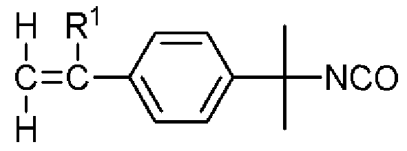
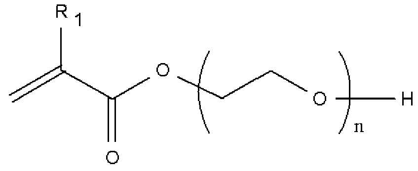
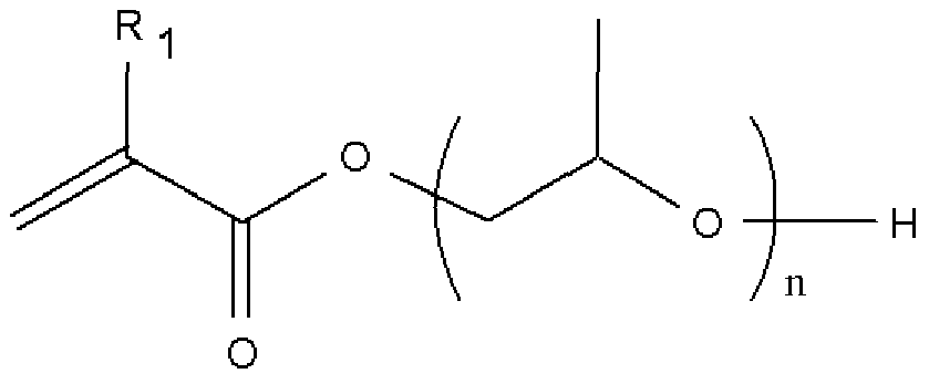
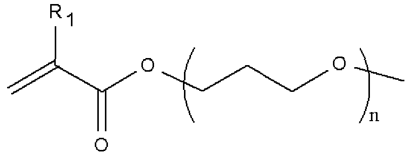


Claims
Priority Applications (1)
| Application Number | Priority Date | Filing Date | Title |
|---|---|---|---|
| US11/597,741 US20080113302A1 (en) | 2004-05-26 | 2005-05-25 | Pattern Forming Process |
Applications Claiming Priority (4)
| Application Number | Priority Date | Filing Date | Title |
|---|---|---|---|
| JP2004156596 | 2004-05-26 | ||
| JP2004-156596 | 2004-05-26 | ||
| JP2005-107956 | 2005-04-04 | ||
| JP2005107956A JP2006011371A (ja) | 2004-05-26 | 2005-04-04 | パターン形成方法 |
Publications (1)
| Publication Number | Publication Date |
|---|---|
| WO2005116774A1 true WO2005116774A1 (ja) | 2005-12-08 |
Family
ID=35451035
Family Applications (1)
| Application Number | Title | Priority Date | Filing Date |
|---|---|---|---|
| PCT/JP2005/009554 Ceased WO2005116774A1 (ja) | 2004-05-26 | 2005-05-25 | パターン形成方法 |
Country Status (5)
| Country | Link |
|---|---|
| US (1) | US20080113302A1 (ja) |
| JP (1) | JP2006011371A (ja) |
| KR (1) | KR20070026649A (ja) |
| TW (1) | TW200611080A (ja) |
| WO (1) | WO2005116774A1 (ja) |
Cited By (1)
| Publication number | Priority date | Publication date | Assignee | Title |
|---|---|---|---|---|
| US9513551B2 (en) | 2009-01-29 | 2016-12-06 | Digiflex Ltd. | Process for producing a photomask on a photopolymeric surface |
Families Citing this family (14)
| Publication number | Priority date | Publication date | Assignee | Title |
|---|---|---|---|---|
| JP4781434B2 (ja) * | 2006-08-03 | 2011-09-28 | 旭化成イーマテリアルズ株式会社 | 感光性樹脂組成物及び積層体 |
| TWI363891B (en) * | 2006-11-14 | 2012-05-11 | Lg Display Co Ltd | Manufacturing method of the flexible display device |
| IL194967A0 (en) * | 2008-10-28 | 2009-08-03 | Orbotech Ltd | Producing electrical circuit patterns using multi-population transformation |
| KR101650878B1 (ko) * | 2010-03-22 | 2016-08-25 | 삼성디스플레이 주식회사 | 박막 트랜지스터의 제조 방법 및 이를 이용한 표시 기판의 제조 방법 |
| WO2013088466A1 (ja) | 2011-12-12 | 2013-06-20 | 三菱電機株式会社 | レーザ光源装置及び映像表示装置 |
| JP7111466B2 (ja) * | 2014-08-01 | 2022-08-02 | アプライド マテリアルズ インコーポレイテッド | 3dパターン形成のためのデジタルグレイトーンリソグラフィ |
| CN114813758A (zh) * | 2014-10-31 | 2022-07-29 | 科磊股份有限公司 | 照明系统、具有照明系统的检验工具及操作照明系统的方法 |
| JP6743021B2 (ja) | 2014-12-31 | 2020-08-19 | ドルビー ラボラトリーズ ライセンシング コーポレイション | 画像プロジェクタ用の個別レーザファイバ入力 |
| TWI545394B (zh) * | 2015-05-29 | 2016-08-11 | Digital roller manufacturing system | |
| KR102097261B1 (ko) * | 2015-08-25 | 2020-04-06 | 아사히 가세이 가부시키가이샤 | 감광성 수지 조성물 |
| CN111279804B (zh) * | 2017-12-20 | 2023-10-24 | 住友电气工业株式会社 | 制造印刷电路板和层压结构的方法 |
| TWI809201B (zh) | 2018-10-23 | 2023-07-21 | 以色列商奧寶科技有限公司 | 用於校正晶粒放置錯誤之適應性路由 |
| JP2022071509A (ja) * | 2020-10-28 | 2022-05-16 | 矢崎総業株式会社 | 防食材、端子付き電線及びワイヤーハーネス |
| US12429769B2 (en) * | 2021-02-09 | 2025-09-30 | Dupont Electronics, Inc. | Photosensitive composition and photoresist dry film made therefrom |
Citations (16)
| Publication number | Priority date | Publication date | Assignee | Title |
|---|---|---|---|---|
| JPH063827A (ja) * | 1992-06-18 | 1994-01-14 | Nec Corp | 厚膜配線パターンの露光法 |
| JPH086246A (ja) * | 1994-06-15 | 1996-01-12 | Tokyo Ohka Kogyo Co Ltd | 耐熱性感光性樹脂組成物 |
| JP2000162767A (ja) * | 1998-11-26 | 2000-06-16 | Hitachi Chem Co Ltd | 感光性樹脂組成物、これを用いた感光性エレメント、レジストパターンの製造法及びプリント配線板の製造法 |
| JP2001040174A (ja) * | 1999-07-29 | 2001-02-13 | Nippon Kayaku Co Ltd | 樹脂組成物、ソルダーレジスト樹脂組成物及びこれらの硬化物 |
| JP2001290014A (ja) * | 2000-04-04 | 2001-10-19 | Nikon Corp | 光学素子の製造方法及び製造システム並びにこの製造方法を用いて製作された光学素子及びこの光学素子を用いた露光装置 |
| JP2002116315A (ja) * | 2000-10-11 | 2002-04-19 | Canon Inc | 微細光学素子の製造方法 |
| JP2002139824A (ja) * | 2000-11-01 | 2002-05-17 | Ricoh Opt Ind Co Ltd | 濃度分布マスク及び多段階露光方法による濃度分布マスクの製造方法 |
| JP2002303974A (ja) * | 1997-11-28 | 2002-10-18 | Hitachi Chem Co Ltd | 光硬化性樹脂組成物及びこれを用いた感光性エレメント |
| JP2003131377A (ja) * | 2001-10-22 | 2003-05-09 | Fuji Photo Film Co Ltd | 層間絶縁膜用感光性樹脂組成物および感光性転写材料 |
| JP2003337425A (ja) * | 2002-05-20 | 2003-11-28 | Fuji Photo Film Co Ltd | 露光装置 |
| JP2003337426A (ja) * | 2002-05-20 | 2003-11-28 | Fuji Photo Film Co Ltd | 露光装置 |
| JP2003337427A (ja) * | 2002-05-20 | 2003-11-28 | Fuji Photo Film Co Ltd | 露光装置 |
| JP2004006440A (ja) * | 2002-04-10 | 2004-01-08 | Fuji Photo Film Co Ltd | レーザ装置、露光ヘッド、及び露光装置 |
| JP2004046003A (ja) * | 2002-07-15 | 2004-02-12 | Seiko Epson Corp | 微細構造体、微細構造体の製造方法及び製造装置 |
| JP2004062156A (ja) * | 2002-06-07 | 2004-02-26 | Fuji Photo Film Co Ltd | 露光ヘッド及び露光装置 |
| JP2005062847A (ja) * | 2003-07-31 | 2005-03-10 | Fuji Photo Film Co Ltd | 露光ヘッド |
Family Cites Families (18)
| Publication number | Priority date | Publication date | Assignee | Title |
|---|---|---|---|---|
| JPS5340537B2 (ja) * | 1974-12-27 | 1978-10-27 | ||
| JPH02186247A (ja) * | 1989-01-12 | 1990-07-20 | Kyushu Electric Power Co Inc | 光学検査装置 |
| JP2769753B2 (ja) * | 1991-08-28 | 1998-06-25 | 株式会社オーク製作所 | 画像形成用露光装置 |
| JP3218658B2 (ja) * | 1992-01-16 | 2001-10-15 | 日立化成工業株式会社 | レジストの製造法 |
| JP3176178B2 (ja) * | 1993-06-25 | 2001-06-11 | 松下電工株式会社 | 回路板製造用マスクおよび回路板の製造方法 |
| US5741624A (en) * | 1996-02-13 | 1998-04-21 | Micron Technology, Inc. | Method for reducing photolithographic steps in a semiconductor interconnect process |
| US6133986A (en) * | 1996-02-28 | 2000-10-17 | Johnson; Kenneth C. | Microlens scanner for microlithography and wide-field confocal microscopy |
| KR100214271B1 (ko) * | 1996-06-29 | 1999-08-02 | 김영환 | 콘택홀용 위상 반전 마스크 |
| JPH113849A (ja) * | 1997-06-12 | 1999-01-06 | Sony Corp | 可変変形照明フィルタ及び半導体露光装置 |
| JP2001305663A (ja) * | 2000-04-20 | 2001-11-02 | Noritsu Koki Co Ltd | 画像焼付装置およびこれを備えた写真処理装置、ならびに画像焼付方法 |
| US6493867B1 (en) * | 2000-08-08 | 2002-12-10 | Ball Semiconductor, Inc. | Digital photolithography system for making smooth diagonal components |
| JP2003029415A (ja) * | 2001-07-06 | 2003-01-29 | Internatl Business Mach Corp <Ibm> | フォトレジスト加工方法及び段型金属体製造方法 |
| JP2003223007A (ja) * | 2002-01-30 | 2003-08-08 | Fuji Photo Film Co Ltd | 平版印刷版の製版方法 |
| JP4731787B2 (ja) * | 2002-04-10 | 2011-07-27 | 富士フイルム株式会社 | 露光ヘッド及び露光装置 |
| JP2003337428A (ja) * | 2002-05-20 | 2003-11-28 | Fuji Photo Film Co Ltd | 露光装置 |
| JP2003344865A (ja) * | 2002-05-22 | 2003-12-03 | Sharp Corp | 液晶用マトリクス基板の製造方法および液晶用マトリクス基板、ならびに電子回路基板の接続部形成方法 |
| JP2004062157A (ja) * | 2002-06-07 | 2004-02-26 | Fuji Photo Film Co Ltd | 光配線回路の製造方法、及びその光配線回路を備えた光配線基板 |
| JP2004240216A (ja) * | 2003-02-06 | 2004-08-26 | Fuji Photo Film Co Ltd | プリント配線板の製造方法 |
-
2005
- 2005-04-04 JP JP2005107956A patent/JP2006011371A/ja active Pending
- 2005-05-25 WO PCT/JP2005/009554 patent/WO2005116774A1/ja not_active Ceased
- 2005-05-25 US US11/597,741 patent/US20080113302A1/en not_active Abandoned
- 2005-05-25 KR KR1020067027255A patent/KR20070026649A/ko not_active Withdrawn
- 2005-05-25 TW TW094117002A patent/TW200611080A/zh unknown
Patent Citations (16)
| Publication number | Priority date | Publication date | Assignee | Title |
|---|---|---|---|---|
| JPH063827A (ja) * | 1992-06-18 | 1994-01-14 | Nec Corp | 厚膜配線パターンの露光法 |
| JPH086246A (ja) * | 1994-06-15 | 1996-01-12 | Tokyo Ohka Kogyo Co Ltd | 耐熱性感光性樹脂組成物 |
| JP2002303974A (ja) * | 1997-11-28 | 2002-10-18 | Hitachi Chem Co Ltd | 光硬化性樹脂組成物及びこれを用いた感光性エレメント |
| JP2000162767A (ja) * | 1998-11-26 | 2000-06-16 | Hitachi Chem Co Ltd | 感光性樹脂組成物、これを用いた感光性エレメント、レジストパターンの製造法及びプリント配線板の製造法 |
| JP2001040174A (ja) * | 1999-07-29 | 2001-02-13 | Nippon Kayaku Co Ltd | 樹脂組成物、ソルダーレジスト樹脂組成物及びこれらの硬化物 |
| JP2001290014A (ja) * | 2000-04-04 | 2001-10-19 | Nikon Corp | 光学素子の製造方法及び製造システム並びにこの製造方法を用いて製作された光学素子及びこの光学素子を用いた露光装置 |
| JP2002116315A (ja) * | 2000-10-11 | 2002-04-19 | Canon Inc | 微細光学素子の製造方法 |
| JP2002139824A (ja) * | 2000-11-01 | 2002-05-17 | Ricoh Opt Ind Co Ltd | 濃度分布マスク及び多段階露光方法による濃度分布マスクの製造方法 |
| JP2003131377A (ja) * | 2001-10-22 | 2003-05-09 | Fuji Photo Film Co Ltd | 層間絶縁膜用感光性樹脂組成物および感光性転写材料 |
| JP2004006440A (ja) * | 2002-04-10 | 2004-01-08 | Fuji Photo Film Co Ltd | レーザ装置、露光ヘッド、及び露光装置 |
| JP2003337425A (ja) * | 2002-05-20 | 2003-11-28 | Fuji Photo Film Co Ltd | 露光装置 |
| JP2003337426A (ja) * | 2002-05-20 | 2003-11-28 | Fuji Photo Film Co Ltd | 露光装置 |
| JP2003337427A (ja) * | 2002-05-20 | 2003-11-28 | Fuji Photo Film Co Ltd | 露光装置 |
| JP2004062156A (ja) * | 2002-06-07 | 2004-02-26 | Fuji Photo Film Co Ltd | 露光ヘッド及び露光装置 |
| JP2004046003A (ja) * | 2002-07-15 | 2004-02-12 | Seiko Epson Corp | 微細構造体、微細構造体の製造方法及び製造装置 |
| JP2005062847A (ja) * | 2003-07-31 | 2005-03-10 | Fuji Photo Film Co Ltd | 露光ヘッド |
Cited By (1)
| Publication number | Priority date | Publication date | Assignee | Title |
|---|---|---|---|---|
| US9513551B2 (en) | 2009-01-29 | 2016-12-06 | Digiflex Ltd. | Process for producing a photomask on a photopolymeric surface |
Also Published As
| Publication number | Publication date |
|---|---|
| TW200611080A (en) | 2006-04-01 |
| JP2006011371A (ja) | 2006-01-12 |
| US20080113302A1 (en) | 2008-05-15 |
| KR20070026649A (ko) | 2007-03-08 |
Similar Documents
| Publication | Publication Date | Title |
|---|---|---|
| WO2005116774A1 (ja) | パターン形成方法 | |
| WO2006028060A1 (ja) | パターン形成材料、並びにパターン形成装置及びパターン形成方法 | |
| JP4546367B2 (ja) | パターン形成材料、並びにパターン形成装置及びパターン形成方法 | |
| JP2006154622A (ja) | パターン形成材料及びパターン形成方法 | |
| JP4500657B2 (ja) | パターン形成材料、並びにパターン形成装置及びパターン形成方法 | |
| JP2005249970A (ja) | パターン形成材料、並びにパターン形成装置及びパターン形成方法 | |
| JP2006220863A (ja) | パターン形成材料、並びにパターン形成装置及びパターン形成方法 | |
| JP4422562B2 (ja) | パターン形成材料、並びにパターン形成装置及びパターン形成方法 | |
| JP2006251385A (ja) | パターン形成材料、並びにパターン形成装置及びパターン形成方法 | |
| JP4546393B2 (ja) | パターン形成材料、並びにパターン形成装置及びパターン形成方法 | |
| JP4485239B2 (ja) | パターン形成方法 | |
| JP2006243546A (ja) | パターン形成材料、並びにパターン形成装置及びパターン形成方法 | |
| JP2006171019A (ja) | パターン形成材料の製造方法及びパターン形成材料 | |
| JP2006251562A (ja) | パターン形成材料、並びにパターン形成装置及びパターン形成方法 | |
| JP2005258431A (ja) | パターン形成方法 | |
| JP4942969B2 (ja) | パターン形成材料及びパターン形成方法 | |
| JP2006184840A (ja) | パターン形成材料、並びにパターン形成装置及びパターン形成方法 | |
| WO2006025389A1 (ja) | パターン形成材料、並びにパターン形成装置及びパターン形成方法 | |
| JP2006003436A (ja) | パターン形成材料、並びにパターン形成装置及びパターン形成方法 | |
| JP2006208734A (ja) | パターン形成方法 | |
| JP2006350038A (ja) | パターン形成方法 | |
| JP2005292336A (ja) | パターン形成材料、並びにパターン形成装置及びパターン形成方法 | |
| JP2006308701A (ja) | パターン形成材料、並びにパターン形成装置及びパターン形成方法 | |
| JP2006292889A (ja) | パターン形成材料、並びにパターン形成装置及びパターン形成方法 | |
| JP2006227221A (ja) | パターン形成材料、及びパターン形成装置並びにパターン形成方法 |
Legal Events
| Date | Code | Title | Description |
|---|---|---|---|
| AK | Designated states |
Kind code of ref document: A1 Designated state(s): AE AG AL AM AT AU AZ BA BB BG BR BW BY BZ CA CH CN CO CR CU CZ DE DK DM DZ EC EE EG ES FI GB GD GE GH GM HR HU ID IL IN IS JP KE KG KM KP KR KZ LC LK LR LS LT LU LV MA MD MG MK MN MW MX MZ NA NG NI NO NZ OM PG PH PL PT RO RU SC SD SE SG SK SL SM SY TJ TM TN TR TT TZ UA UG US UZ VC VN YU ZA ZM ZW |
|
| AL | Designated countries for regional patents |
Kind code of ref document: A1 Designated state(s): BW GH GM KE LS MW MZ NA SD SL SZ TZ UG ZM ZW AM AZ BY KG KZ MD RU TJ TM AT BE BG CH CY CZ DE DK EE ES FI FR GB GR HU IE IS IT LT LU MC NL PL PT RO SE SI SK TR BF BJ CF CG CI CM GA GN GQ GW ML MR NE SN TD TG |
|
| 121 | Ep: the epo has been informed by wipo that ep was designated in this application | ||
| NENP | Non-entry into the national phase |
Ref country code: DE |
|
| WWW | Wipo information: withdrawn in national office |
Country of ref document: DE |
|
| WWE | Wipo information: entry into national phase |
Ref document number: 200580020670.9 Country of ref document: CN |
|
| WWE | Wipo information: entry into national phase |
Ref document number: 1020067027255 Country of ref document: KR |
|
| WWP | Wipo information: published in national office |
Ref document number: 1020067027255 Country of ref document: KR |
|
| 122 | Ep: pct application non-entry in european phase | ||
| WWE | Wipo information: entry into national phase |
Ref document number: 11597741 Country of ref document: US |
|
| NENP | Non-entry into the national phase |
Ref country code: JP |
|
| WWW | Wipo information: withdrawn in national office |
Country of ref document: JP |
|
| WWP | Wipo information: published in national office |
Ref document number: 11597741 Country of ref document: US |