WO2004104662A1 - 光デバイス及び光デバイスの製造方法、ならびに光集積デバイス - Google Patents
光デバイス及び光デバイスの製造方法、ならびに光集積デバイス Download PDFInfo
- Publication number
- WO2004104662A1 WO2004104662A1 PCT/JP2004/007136 JP2004007136W WO2004104662A1 WO 2004104662 A1 WO2004104662 A1 WO 2004104662A1 JP 2004007136 W JP2004007136 W JP 2004007136W WO 2004104662 A1 WO2004104662 A1 WO 2004104662A1
- Authority
- WO
- WIPO (PCT)
- Prior art keywords
- light
- optical
- refractive index
- optical transmission
- transmission line
- Prior art date
Links
Classifications
-
- G—PHYSICS
- G02—OPTICS
- G02F—OPTICAL DEVICES OR ARRANGEMENTS FOR THE CONTROL OF LIGHT BY MODIFICATION OF THE OPTICAL PROPERTIES OF THE MEDIA OF THE ELEMENTS INVOLVED THEREIN; NON-LINEAR OPTICS; FREQUENCY-CHANGING OF LIGHT; OPTICAL LOGIC ELEMENTS; OPTICAL ANALOGUE/DIGITAL CONVERTERS
- G02F1/00—Devices or arrangements for the control of the intensity, colour, phase, polarisation or direction of light arriving from an independent light source, e.g. switching, gating or modulating; Non-linear optics
- G02F1/29—Devices or arrangements for the control of the intensity, colour, phase, polarisation or direction of light arriving from an independent light source, e.g. switching, gating or modulating; Non-linear optics for the control of the position or the direction of light beams, i.e. deflection
- G02F1/31—Digital deflection, i.e. optical switching
- G02F1/313—Digital deflection, i.e. optical switching in an optical waveguide structure
- G02F1/3136—Digital deflection, i.e. optical switching in an optical waveguide structure of interferometric switch type
-
- G—PHYSICS
- G02—OPTICS
- G02B—OPTICAL ELEMENTS, SYSTEMS OR APPARATUS
- G02B6/00—Light guides; Structural details of arrangements comprising light guides and other optical elements, e.g. couplings
- G02B6/24—Coupling light guides
- G02B6/26—Optical coupling means
- G02B6/28—Optical coupling means having data bus means, i.e. plural waveguides interconnected and providing an inherently bidirectional system by mixing and splitting signals
-
- G—PHYSICS
- G02—OPTICS
- G02B—OPTICAL ELEMENTS, SYSTEMS OR APPARATUS
- G02B6/00—Light guides; Structural details of arrangements comprising light guides and other optical elements, e.g. couplings
- G02B6/10—Light guides; Structural details of arrangements comprising light guides and other optical elements, e.g. couplings of the optical waveguide type
- G02B6/12—Light guides; Structural details of arrangements comprising light guides and other optical elements, e.g. couplings of the optical waveguide type of the integrated circuit kind
- G02B6/13—Integrated optical circuits characterised by the manufacturing method
- G02B6/138—Integrated optical circuits characterised by the manufacturing method by using polymerisation
-
- G—PHYSICS
- G02—OPTICS
- G02B—OPTICAL ELEMENTS, SYSTEMS OR APPARATUS
- G02B6/00—Light guides; Structural details of arrangements comprising light guides and other optical elements, e.g. couplings
- G02B6/24—Coupling light guides
-
- G—PHYSICS
- G02—OPTICS
- G02B—OPTICAL ELEMENTS, SYSTEMS OR APPARATUS
- G02B6/00—Light guides; Structural details of arrangements comprising light guides and other optical elements, e.g. couplings
- G02B6/24—Coupling light guides
- G02B6/26—Optical coupling means
- G02B6/28—Optical coupling means having data bus means, i.e. plural waveguides interconnected and providing an inherently bidirectional system by mixing and splitting signals
- G02B6/2804—Optical coupling means having data bus means, i.e. plural waveguides interconnected and providing an inherently bidirectional system by mixing and splitting signals forming multipart couplers without wavelength selective elements, e.g. "T" couplers, star couplers
- G02B6/2808—Optical coupling means having data bus means, i.e. plural waveguides interconnected and providing an inherently bidirectional system by mixing and splitting signals forming multipart couplers without wavelength selective elements, e.g. "T" couplers, star couplers using a mixing element which evenly distributes an input signal over a number of outputs
- G02B6/2813—Optical coupling means having data bus means, i.e. plural waveguides interconnected and providing an inherently bidirectional system by mixing and splitting signals forming multipart couplers without wavelength selective elements, e.g. "T" couplers, star couplers using a mixing element which evenly distributes an input signal over a number of outputs based on multimode interference effect, i.e. self-imaging
-
- G—PHYSICS
- G02—OPTICS
- G02B—OPTICAL ELEMENTS, SYSTEMS OR APPARATUS
- G02B6/00—Light guides; Structural details of arrangements comprising light guides and other optical elements, e.g. couplings
- G02B6/10—Light guides; Structural details of arrangements comprising light guides and other optical elements, e.g. couplings of the optical waveguide type
- G02B6/12—Light guides; Structural details of arrangements comprising light guides and other optical elements, e.g. couplings of the optical waveguide type of the integrated circuit kind
- G02B2006/12083—Constructional arrangements
- G02B2006/12095—Graded
-
- G—PHYSICS
- G02—OPTICS
- G02B—OPTICAL ELEMENTS, SYSTEMS OR APPARATUS
- G02B6/00—Light guides; Structural details of arrangements comprising light guides and other optical elements, e.g. couplings
- G02B6/24—Coupling light guides
- G02B6/26—Optical coupling means
- G02B6/30—Optical coupling means for use between fibre and thin-film device
-
- G—PHYSICS
- G02—OPTICS
- G02B—OPTICAL ELEMENTS, SYSTEMS OR APPARATUS
- G02B6/00—Light guides; Structural details of arrangements comprising light guides and other optical elements, e.g. couplings
- G02B6/24—Coupling light guides
- G02B6/42—Coupling light guides with opto-electronic elements
- G02B6/4201—Packages, e.g. shape, construction, internal or external details
- G02B6/4204—Packages, e.g. shape, construction, internal or external details the coupling comprising intermediate optical elements, e.g. lenses, holograms
- G02B6/4214—Packages, e.g. shape, construction, internal or external details the coupling comprising intermediate optical elements, e.g. lenses, holograms the intermediate optical element having redirecting reflective means, e.g. mirrors, prisms for deflecting the radiation from horizontal to down- or upward direction toward a device
-
- G—PHYSICS
- G02—OPTICS
- G02F—OPTICAL DEVICES OR ARRANGEMENTS FOR THE CONTROL OF LIGHT BY MODIFICATION OF THE OPTICAL PROPERTIES OF THE MEDIA OF THE ELEMENTS INVOLVED THEREIN; NON-LINEAR OPTICS; FREQUENCY-CHANGING OF LIGHT; OPTICAL LOGIC ELEMENTS; OPTICAL ANALOGUE/DIGITAL CONVERTERS
- G02F1/00—Devices or arrangements for the control of the intensity, colour, phase, polarisation or direction of light arriving from an independent light source, e.g. switching, gating or modulating; Non-linear optics
- G02F1/01—Devices or arrangements for the control of the intensity, colour, phase, polarisation or direction of light arriving from an independent light source, e.g. switching, gating or modulating; Non-linear optics for the control of the intensity, phase, polarisation or colour
- G02F1/21—Devices or arrangements for the control of the intensity, colour, phase, polarisation or direction of light arriving from an independent light source, e.g. switching, gating or modulating; Non-linear optics for the control of the intensity, phase, polarisation or colour by interference
- G02F1/217—Multimode interference type
-
- G—PHYSICS
- G02—OPTICS
- G02F—OPTICAL DEVICES OR ARRANGEMENTS FOR THE CONTROL OF LIGHT BY MODIFICATION OF THE OPTICAL PROPERTIES OF THE MEDIA OF THE ELEMENTS INVOLVED THEREIN; NON-LINEAR OPTICS; FREQUENCY-CHANGING OF LIGHT; OPTICAL LOGIC ELEMENTS; OPTICAL ANALOGUE/DIGITAL CONVERTERS
- G02F1/00—Devices or arrangements for the control of the intensity, colour, phase, polarisation or direction of light arriving from an independent light source, e.g. switching, gating or modulating; Non-linear optics
- G02F1/29—Devices or arrangements for the control of the intensity, colour, phase, polarisation or direction of light arriving from an independent light source, e.g. switching, gating or modulating; Non-linear optics for the control of the position or the direction of light beams, i.e. deflection
- G02F1/31—Digital deflection, i.e. optical switching
- G02F1/313—Digital deflection, i.e. optical switching in an optical waveguide structure
- G02F1/3137—Digital deflection, i.e. optical switching in an optical waveguide structure with intersecting or branching waveguides, e.g. X-switches and Y-junctions
Definitions
- the present invention relates to a method for manufacturing an optical fiber and a light source having a sheet-like transmission line used for high-speed multi-mode and optical transmission, and more specifically, to an optical branching method.
- Multi-mode K suitable for photosynthesis, optical demultiplexer, optical filter, optical straight-through synth, optical x-ray, stapler, optical switch, etc.
- the present invention also relates to an optical disk and a method of manufacturing an optical disk using the principle of self-imaging of interference, and the present invention also relates to an optical disk having a plurality of the above optical disks.
- Multimode optical transmission lines are cheaper than single mode optical transmission lines and can be replaced with conventional electronic circuits.
- Multimode, optical transmission path, S G-shaped multimode, optical transmission path Example 7L, Wen (3) has a uniform refractive index Light-emitting body, a laser diode for inputting signal light to the incident end face of the light-emitting medium, an array, and a photo diode for receiving signal light emitted from the light-emitting end face of the transparent medium.
- An optical circuit board provided with a code and an array is disclosed. O
- a laser diode and an array are used. The emitted incident light repeats total reflection in the thickness direction and the width direction inside the transparent medium, exits from the entire area of the exit side end face as exit light, and is output as a photo diode. Received in one K array 0
- Document (2) like Document (3), is composed of a sheet-like transparent medium having a uniform refractive index, a laser diode for injecting signal light into a transparent medium, and a transparent sheet.
- the present invention discloses an optical branching device provided with a plurality of optical fins for receiving signal light emitted from a conductive medium, and the optical branching device described in Document (2) has a light incident side.
- the signal light is diffused inside the transparent medium.
- the incident light is transmitted in the thickness direction and the width direction inside the transparent medium. Repeated total reflection is emitted as emission light from the entire area of the emission side surface, and is received by the photodiode and array 0
- Document (1) also has a sheet-like photon having a maximum refractive index at the center in the thickness direction and a refractive index distribution that decreases as the distance from the center increases. 1 ⁇ J of the tanos o reference (
- the light source described in 1) is described as reducing the K dispersion of the multi-molecule by the refractive index distribution. Is emitted as outgoing light from the entire area of the outgoing end face o
- an optical waveguide for transmitting signal light in a multi-mode in a width direction is provided between a single-mode optical transmission line on an incident side and a single-mode optical transmission line on an exit side.
- the optical waveguide has a constant refractive index n of the optical waveguide and a basic mode width w in the width direction of the optical waveguide.
- ⁇ an optical waveguide having a predetermined length L determined from the wavelength ⁇ of the signal light to be transmitted, is based on the length L in the length of the signal light.
- Intrinsic modes generate emitted light by interfering with each other along the length direction (References (4) to (8), (11))
- Wavelength division multiplexing transmission (W a )
- optical demultiplexing for demultiplexing signal light of different wavelengths In the M system, optical demultiplexing for demultiplexing signal light of different wavelengths
- Optical fibers such as optical multiplexing that combine signal lights of different wavelengths play an important role.
- Such an optical demultiplexer and optical splitter are connected to the single-mode optical transmission line on the input side and the single-mode optical transmission line on the output side by a manhole mode in the width direction.
- These conventional optical demultiplexers and splitters combine an incident-side single-mode waveguide and an optical waveguide that is connected to the incident-side single-mode waveguide and transmits in multi-mode in the width direction.
- ⁇ is a single-mode
- the two-wavelength winter signal light that is mutually adjacent to the waveguide is transmitted and incident on the optical waveguide.
- the eigenwaves of the signal light are emitted from the optical waveguide by interfering with each other along the length direction.
- the width of the optical waveguide and the length of the optical waveguide are set so as to generate light emitted from different positions on the edge.
- Reference (10) shows a method for manufacturing an optical ⁇ path including an incident-side beam converting section, an optical waveguide section, and an emitting-side beam converting section.
- the method of manufacturing the optical fiber of No. 1) described that an optical waveguide was formed by sealing a fluid material in a glass plate. In particular, the incident side beam converter and the output side beam converter are refracted.
- the physical optical path length (phase speed) differs for each mode, and the intensity distribution of the emitted light depends on the length of the optical transmission path due to the la o. If the optical transmission path of O or Multimode, where the changing phenomenon occurs, is too long to exceed 100 m, the optical path. The light signal waveform changes, causing a phenomenon.
- phase dispersion and group velocity are different between the modes and the dispersion is caused by the decrease as in-, the intensity of the incident light is transmitted while maintaining the intensity on the output side.
- a refractive index component is applied.
- Document (1) discloses an optical antenna having stacked sheet-like optical transmission lines and having a refractive index distribution in the direction in which the sheet-like optical transmission lines are stacked. It is described. Since the mode of the optical transmission line described in the literature (1) is suppressed by the refractive index distribution, the mode and the dispersion are suppressed, so that a multimode high-frequency signal of a gigabit class is transmitted. If you do, o
- An optical device such as-requires a configuration to allow signal light to enter the sheet-like optical transmission line and to emit the signal light from the sheet-like optical transmission line. o
- the optical noise described in the above-mentioned document (1) and the signal light is incident parallel to the transmission direction of the signal light from the-end of the optical transmission line. Then, the signal light is emitted from the other end of the sheet-like optical transmission line in parallel with the transmission direction of the signal light (FIGS. 1 and 9 in Document (1)).
- the multi-modal optical path described in the literatures (2) and (3) is an incident light that is incident as signal light.
- the multi-mode and optical transmission lines described in 3) are designed to perform high transmission such that transmission speed is limited by general diffusion of incident light and exceeds 10 GbPS.
- the light V node described in the literature (1) has a refractive index component in the thickness direction, the mode and dispersion in the thickness direction are suppressed, but the width is small. Since the index of refraction is constant in the direction, mode and dispersion occur in the width direction, and the transmission speed is similarly limited. All of the technologies mounted on the board emit light as emission light from the entire area of the end face of the emission side. The problem of great loss was found
- optical waveguides described in Documents (4) to (8) to (11) are designed to receive single-mode signal light in the zonal direction.
- ⁇ Although a can be transmitted at high speed with a small loss of ⁇ , it can be transmitted at a high speed, but even in a single mode, the signal light has a large diffusion ⁇ a large angle and a large angle.
- incident light with a large beam size such as light, masolechi mode, or light emitted from a waveguide, it is difficult to connect to the optical waveguide because it is difficult to connect to the optical waveguide. The problem was when the loss of signal light was significant. Also ⁇
- optical waveguides described in the literatures (4), (8) and (11) have an axis offset with respect to the center of the optical waveguide. Because of the large loss, it was necessary to match the incoming and outgoing light with the incoming and outgoing light with high accuracy and precision.
- optical waveguides described in the literatures (4) to (8) (11) are used in a thickness direction in such a manner that a signal light, which is a multi-mode, is incident on the optical waveguide. If the divergence is large, the divergence angle is large, and the incoming and outgoing light Although difficult, the problem will be revised,
- the method of manufacturing the optical path described in the literature (10) is not an example in which the optical waveguide has a refractive index distribution.
- An example in which a refractive index distribution is provided is disclosed. Accordingly, the process of manufacturing an internal optical waveguide + in the method for manufacturing an optical device described in Reference (10) is disclosed. (1), (2), (4)-(9), (11)
- the width in the width and the length in the length direction are specified so as to have a lens function, using the process of manufacturing the inner beam conversion part of the method. Therefore, it is not possible to obtain a multi-mode, optical waveguide that generates interference, and it is not possible to obtain an optical waveguide that is described in the literature (10).
- the method of manufacturing the conversion section is a method of forming a refractive index distribution in an optical waveguide because the method of forming a refractive index distribution in an optical waveguide is a method of sequentially forming materials having different refractive indexes.
- the first object of the present invention is to input and output signal light.
- a first object of the present invention is to provide a method of manufacturing an optical integrated device and an optical integrated V bus having a plurality of the light ⁇ nodes.
- the first target is composed of the following first optical V-noise.
- An optical ⁇ -noise that is in contact with the signal light between the input signal input from the outside and the output output signal is defined as:
- the sheet has a maximum refractive index portion in the thickness direction of the sheet, and the refractive index does not increase as the distance from the maximum refractive index portion in the thickness direction increases.
- the signal light corresponding to the input signal is made to enter as the optical transmission line incident light
- a multi-mode device having a plurality of eigenmodes in the width direction orthogonal to both the length direction and the thickness direction in the length direction orthogonal to the thickness direction.
- a plurality of eigenmodes generate an outgoing light by interfering with each other in the longitudinal direction by IP.
- It is characterized by emitting outgoing light from an optical transmission line and outputting an output signal corresponding to the outgoing light.
- the first optical node according to the present invention is a multi-mode optical signal transmission device, since the optical transmission line has a refractive index in the thickness direction. Also, the dispersion in the thickness direction is suppressed.
- the optical bus according to the present invention is capable of transmitting and receiving signal light at high speed. At the time of Low loss ⁇ High-precision adjustment is not required when connecting ⁇
- the optical transmission line is a 1 ⁇ J number of a difference between the propagation constant of the 0th-order module K excited in the width direction of the optical transmission line and the propagation constant of the 1st-order module. 0 with the magnitude in the length direction represented
- the optical transmission line is based on the basic module width in the width direction, the effective refractive index for the 0th order light excited in the width direction, the wavelength of light transmitted through the multi-mode optical transmission path, 0 with lengthwise magnitude expressed by the function of
- the optical transmission line has a maximum bending at the center position in the vertical direction.
- /-Refractive index away from the center position.
- the refractive index distribution can vary approximately with the quadratic function. 0
- the optical transmission line is made of Pozi silane.
- the optical transmission line is made of Pozi silane, and the Po V silane is hardened.
- the refractive index distribution is given by the oxygen concentration distribution of o
- the input signal is an electric signal
- the air signal is converted into a signal light
- an input section is provided for inputting the signal light as light incident on an optical transmission line.
- the incident portion has a plurality of light emitting portions arranged in an array in the width direction of the optical transmission line.
- the input signal is applied to a signal light, and an input portion for inputting the signal light to the optical transmission line as incident light is provided.
- the output signal is a signal
- the emission unit has an array shape in the width direction of the light transmission path.
- the output signal is a signal light, and an output section is provided for emitting the signal light from the optical transmission line as the output light.
- the optical transmission path is a
- An incident surface for receiving incident light and
- the magnitude of the length direction I indicates that the basic mode width in the width direction is W, the effective refractive index for the 0th-order mode light pumped in the width direction is n, and the transmission through the multi-mode optical transmission line.
- the wavelength of the light to be emitted is ⁇
- the value is substantially an integral multiple of the following equation, and one incident light is incident on the incident surface and at the center in the width direction.
- the light path is a
- An incident surface for receiving incident light, and And an emission surface for emitting the emitted light An incident surface for receiving incident light, and And an emission surface for emitting the emitted light.
- the size in the length direction is W, and the width of the basic mode in the width direction is W.
- n is the effective refractive index for the zero-order mode light pumped in the width direction
- ⁇ is the wavelength of the light transmitted through the multi-mode optical transmission line. This is a value that is an integral multiple, and ⁇ incident light beams having all wavelengths ⁇ on the incident surface and symmetrically with respect to the center in the width direction are incident on the exit surface.
- the optical device is ⁇ (N 1? 2, 3 • hot ⁇
- An incident surface for receiving incident light and
- the magnitude of 1 in the length direction means that the basic mode width in the width direction is W 0, and the width in the width direction is 0 0 th mode, and the effective refractive index of the excited light is n 0 and ⁇ multi mode. Assuming that the wavelength of light transmitted through the optical transmission path is ⁇ , the value is almost an integral multiple of the following expression, and
- the optical device is ⁇ (see ⁇ 1, 2, 3) « «
- the size is 1 in the length direction and W is the basic mode width in the width direction.
- the effective refractive index of the excited 0th-order mode light is ⁇ 0, and ⁇ the wavelength of light transmitted through the multi-mode optical transmission line is L; Is an odd multiple of the formula
- ⁇ pieces of incident light having the same wavelength ⁇ are incident on the incident surface and at any positions in the width direction, and the incident position of each incident light and the width of the incident light Generates ⁇ outgoing lights corresponding to ⁇ incoming lights and 1 to 1 at positions where the positions are symmetrical with respect to the center in the width direction.
- the optical signal is input to ⁇ ( ⁇ 12, 3 input signals, and
- the optical transmission line is a single power plug that outputs as ⁇ output signals.
- An incident surface for receiving incident light and
- the size in the length direction is W and the basic mode width in the width direction is W.
- the actual halo m-fold rate of light is n.
- L is the wavelength of light transmitted in the Manolechi mode optical transmission line, the value is approximately the following equation.
- ⁇ pieces of incident light having the same wavelength ⁇ are made incident at all predetermined positions in the width direction on the incident surface, and on the exit surface, the incident position of each incident light and the width direction are different. Generate ⁇ outgoing light for any one of the incoming light at each position where the position is symmetrical with respect to the center in the width direction ⁇ (An integer that makes the inside of Katsuko positive)
- the optical noise is ⁇ E V E N (N E V E N
- NEVE incident light having the same wavelength; I is incident on the incident surface and symmetrically with respect to the center in the width direction.
- a star coupler that outputs as DD output signals.
- N 0 4 1 4 1 incident light having the same wavelength; I is incident on the incident surface and at an asymmetric position at the center in the width direction.
- the optical noise is N (N2 3 ) Input signals and can be output as N output signals corresponding to the first input signal M (M
- the optical transmission path is a
- the first surface formed at one end in the length direction
- the length in the length direction including the second surface formed at the other end in the length direction is w
- the basic mode width in the width direction is w.
- ⁇ incident lights having the same wavelength ⁇ are made incident at all positions in the width direction on the first surface, and the incident position of each incident light and the width direction are incident on the second surface. At each of the same positions, N outgoing light beams corresponding to ⁇ incoming light beams are generated, one by one.
- First input signals, and 1 Can be output as one-to-one or one-to-one output signal
- M ( ⁇ 1, 2, 3 • • •) second input signals are input, and both can be output as M output signals corresponding to the second input signals on a one-to-one basis.
- Optical transmission line Optical transmission line.
- the size in the length direction is equal to the width direction.
- W is the basic mode width.
- a total of ⁇ incident lights having the same wavelength ⁇ are made incident at any given position in the width direction on one surface, and the incident positions of each incident light and the width direction are made on the second surface. Each time the position becomes symmetrical with respect to the center in the width direction, ⁇ outgoing lights corresponding to N incoming lights and 1 to 1 are generated, respectively.
- ⁇ incident lights having the same wavelength ⁇ are incident on all the arbitrary positions in the width direction on the two surfaces, and the incident position of each incident light on the first surface and the width direction are incident on the first surface.
- the optical transmission path is formed at one end in the length direction and is an optical path of incident light incident along a direction parallel to the thickness direction.
- Reflection surface and / or length that bends approximately 90 in the length direction The optical path of the emitted light formed at the other end in the vertical direction and transmitted along the longitudinal direction is emitted along a direction parallel to the thickness direction. Includes reflective surface
- the optical transmission line is formed at one end in the longitudinal direction and bends the optical path of the incident light incident along the direction inclined in the thickness direction in the longitudinal direction.
- a prism, and / or an optical path of emitted light formed at the other end in the length direction and transmitted along the length direction is emitted along a direction inclined in the thickness direction. It has a bending curve.
- the optical transmission line has a plurality of eigenmodes in the thickness direction.With the configuration of-, multi-mode and optical noise utilizing interference are also provided in the thickness direction.
- the optical transmission line has a thickness of 20 m or more.
- the optical transmission path is curved so that the center position in the thickness direction always draws the same curve in two different cross sections including the length direction and the thickness direction.
- the optical transmission path has two different cross sections including the length direction and the thickness direction, and the center position in the thickness direction draws different curves. ⁇ Twisted like
- the first purpose is to be realized by the following optical integrated device
- An optical integrated device that is connected by signal light between the input signal input from the outside and the output smoothness, and is in the form of a sheet, and has a thickness of the sheet.
- An optical transmission line including a refractive index distribution having a maximum refractive index portion in the direction, and the refractive index does not increase as the distance from the maximum refractive index portion increases in the thickness direction. It has a light transmission section that is formed by shelling in the direction of
- the signal light corresponding to the input signal is emitted to each optical transmission line as incident light,
- a multi-mode having multiple eigenmodes in the width direction orthogonal to both the length direction and the thickness direction along the length direction orthogonal to the thickness direction.
- a plurality of eigenmodes generate outgoing light by interfering with each other in the longitudinal direction.
- ⁇ is characterized by emitting outgoing light from each optical transmission line and outputting an outlet corresponding to the outgoing light.
- the optical concentrator antenna according to the present invention has a multimode transmission of signal light since each optical transmission line has a refractive index distribution in the thickness direction. Mode in the thickness direction, dispersion is suppressed
- the signal light can be transmitted at a high speed, and the optical concentrator noise according to the present invention generates outgoing light due to multi-mode interference in each optical transmission line.
- the first one hundred basis is the following by X) ⁇ to 1 of the production method the first m of light ⁇ Roh office o
- a method for manufacturing a light-emitting device for connecting an input signal input from the outside and an output signal to be output by signal light comprising:
- the sheet has a large refractive index portion in the transverse direction of the sheet, and the refractive index does not increase as the distance from the maximum refractive index portion in the thickness direction increases.
- Optical transmission including rate distribution Have a road ⁇
- the signal light corresponding to the input signal is emitted to the optical transmission line as incident light.
- a multi-mode having a plurality of eigenmodes in the width direction orthogonal to both the length direction and the thickness direction along the length direction orthogonal to the thickness direction.
- a plurality of eigenmodes interfere with each other along the length direction to generate the outgoing light
- a third port for applying a predetermined amount of energy from above and below in the thickness direction to the resin-filled molding die
- a small ⁇ and 'length in the length direction is determined to form the connection part of the incoming and outgoing light.
- the application of energy is irradiation of the outside line of a predetermined wavelength.
- the mold to be prepared is made of a material that is transparent to the external line of the specified wavelength.
- the optical transmission line has a maximum refractive index at the center position in the thickness direction, and includes a refractive index component whose refractive index does not increase as the distance from the center position increases.
- the refractive index distribution varies ⁇ almost quadratic 0
- the optical transmission path is made of Pozi silane, and the optical transmission path is made of Po V silane.
- the mold includes a recess having a size that includes a plurality of manufacturing 1K optical transmission paths,
- the molding is performed in the following manner.
- the size is approximately equal in the width direction of the optical transmission line.
- the mold includes a recess having a size substantially equal to the optical transmission path, and
- the incident light and the outgoing light are made to enter and exit the optical transmission line.
- the method of manufacturing the optical V-noise of the present invention includes O It is possible to perform a stowdown at the time of manufacture because the use is strong o
- a multiplexed signal light in which two different wavelengths are overlapped and input is input, and the multiplexed signal light can be demultiplexed according to the wavelength and output as two different signal lights.
- the sheet has a maximum refractive index portion in the thickness direction of the sheet.
- the optical transmission path includes the refractive index component, and the refractive index does not increase as the distance from the large refractive index portion increases along the thickness direction.
- the multiplexed signal light is made to enter the optical transmission line as incident light,
- Incoming light is transmitted by multi-mode K, which has multiple eigenmodes for each wavelength, and multiple eigenmodes are transmitted in the longitudinal direction for signal light of the same wavelength.
- multi-mode K which has multiple eigenmodes for each wavelength, and multiple eigenmodes are transmitted in the longitudinal direction for signal light of the same wavelength.
- the second optical node according to the present invention has a configuration in which a signal light is transmitted in a multi-mode because the optical transmission line has a refractive index in the thickness direction. Mode and dispersion are suppressed in the thickness direction
- the optical antenna according to the present invention is capable of transmitting signal light at high speed, and the optical transmission line generates multi-mode light, emits light by interference, and responds to the wavelength.
- the loss of light is small at the time of input and output.
- the two outgoing light beams are emitted from the widthwise position where the ratio of the light amounts of each other is maximized.
- the two outgoing light beams have the light intensity of each other. Emitted from the minimum width direction o
- the optical transmission line is excited in the width direction of the optical transmission line.
- the optical transmission line has a rectangular parallelepiped shape, a basic mode in the width direction, a large refractive index in the width and width directions, a multimode, and a wavelength of light transmitted through the optical transmission line.
- ⁇ has a length dimension expressed by the function of and
- the optical transmission line has a maximum refractive index at the center position in the thickness direction, and includes a refractive index component whose refractive index does not increase with distance from the position. It is desirable that the fraction change approximately with the quadratic function o
- optical fibers described in the literatures (9) and (12) and (15) are optical waveguides that perform optical branching and transmit multi-mode signal light only in the width direction. It has the same problems as in the literatures (4) to (8) and (11). In other words, even in a single mode, signal light has a large degree of diffusion ⁇ a wide angle, a multiplexed signal light, or a multiplexed signal light with a large beam diameter is used. In the field a, there was a problem that the loss of the signal light at the time of entering and exiting was large due to the difficulty of the aperture ⁇ to the optical waveguide.
- the axis a with respect to the center of the optical waveguide It is necessary to make the incident multiplexed signal light and the outgoing signal light into the input and output side with high accuracy as ⁇ because the error is large with respect to the incident light which is shifted and o
- optical waveguide described in the light source described in the literatures (9) and (12) to (15) is multiplexed in the thickness direction with a multi-modal multi-K optical signal. ⁇ Mode and dispersion occur in the thickness direction ⁇ High-speed transmission is not possible o
- the second object of the present invention is to provide a mechanism for transmitting and receiving signal light.
- An object of the present invention is to provide an optical noise source capable of high-speed transmission of 10 GbS and capable of satisfactorily demultiplexing and multiplexing multiplexed signal light.
- the second giant is achieved by the third optical disk below.
- Optical sheet having a large refractive index portion in the thickness direction of the sheet, and extending along the thickness direction from the maximum refractive index portion.
- An optical transmission path including a refractive index component whose refractive index does not increase with distance
- the two signal lights are made incident as light incident on the optical transmission line, and both inside the optical transmission line and in the length direction and the thickness direction along the length direction orthogonal to the child direction. Width direction orthogonal to
- the third optical path according to the present invention is characterized in that the optical transmission path bends in the thickness direction, and the distribution of bending ratio is not provided. Even in a multi-mode configuration in which signal light is transmitted, mode and dispersion are suppressed in the thickness direction.
- the optical signal according to the present invention has a multimode optical transmission line that emits light by interference and generates light according to the wavelength.
- the optical transmission line described in Refs. (1) to (8) and (11) does not require high-precision adjustment for connection.
- the optical waveguides are designed to emit outgoing light uniquely in response to incident light, and therefore, by using an optical transmission line or an optical waveguide, No technical idea has been suggested for sizing to select the emission position of the outgoing light corresponding to the incident light.
- the third embodiment of the present invention is capable of easily coupling when inputting and outputting signal light.
- An optical signal that is connected to the signal light between the input signal input from the outside and the output signal to be output.
- the sheet has a maximum refractive index portion in the thickness direction of the sheet, and the refractive index increases as the distance from the maximum refractive index portion in the thickness direction increases.
- optical transmission line consisting of the partial optical transmission line 2 and 2
- a refractive index modulating means capable of changing a small one of the first and second partial optical transmission lines based on a control signal supplied from the outside;
- the signal light corresponding to the input signal is made incident as the first light transmission path incident light
- the first state which is the first state, inside the first optical transmission line, a plurality of eigenmodes in the width direction along the length direction orthogonal to the thickness direction and the width direction,
- the incident light is transmitted by the multi-mode K with
- Incident light is transmitted inside the first and second optical transmission lines in a multi-mode having a plurality of unique modes in the width direction along the thickness direction.
- a plurality of eigenmodes interfere with each other in the longitudinal direction to generate mountain light
- the fourth optical device has a configuration in which the optical transmission line has a refractive index distribution in the thickness direction, so that the signal light is transmitted and transmitted in a multi-mode, and the mode dispersion in the thickness direction is performed. Is suppressed
- the optical ap- paratus according to the present invention has a multi-mode optical transmission line, which emits outgoing light by interference and generates a switching light. Therefore, the loss at the time of input and output is small. ⁇ The connection at the time of connection does not require a high degree of adjustment.
- Jo equalizes the refractive index components of the first and second multimode spectral transmission paths
- the maximum refractive index of the Manorechimo K partial optical transmission line is set to be larger than the maximum refractive index of the second multi-mode partial optical transmission line.
- the refractive index modulating means is
- the refractive index distribution of the partial optical transmission line can be changed.
- the maximum refractive index of the second multi-mode and partial optical transmission line is smaller than the maximum refractive index of the first multi-mode and partial optical transmission line, and the optical device described in claim 49.
- the refractive index modulating means comprises:
- the first and second Manoreti mode spectroscopy is performed to equalize the refractive index distribution of the transmission path
- the maximum refractive index of the first Manoretimode partial optical transmission line is larger than the maximum refractive index of the second multimode and partial optical transmission line in the second state.
- the maximum refractive index of the second multi-mode partial optical transmission line is made smaller than the maximum refractive index of the first multi-mode partial optical transmission line in the second state.
- the optical transmission line whose refractive index distribution can be changed by the refractive index modulator 5 is a heat transmission line.
- the refractive index modulator includes a cooling sheet capable of generating and absorbing heat in response to a control signal,
- the refractive index distribution is changed by changing the temperature of the light transmission path by a cold sheet o
- the optical transmission path is
- the size in the length direction is such that the basic mode width in the width direction of the transmission line is W 0, the width direction is [0: the second-order excited zero-order mode, the effective refractive index of the light is n 0, and the first. ⁇
- the wavelength of light transmitted through the second optical transmission path is ⁇ , the value is almost an odd multiple of the following equation.
- the optical transmission line is
- the output light can be generated by the multi-mode and interference in the state 2 due to the composition of o
- the optical transmission line includes a refractive index distribution in which the refractive index is the maximum at the central position in the vertical direction, and the refractive index does not increase with distance from the central position.o
- each refractive index distribution changes along the quadratic function.0
- the optical waveguides described in References (4) to (8) and (11) have an input side and an output side. Both optical waveguides have a single mode (the core diameter is less than 10 ⁇ m), and therefore interfere with different eigenmodes in the width direction. Id, interference
- the separation interval of the emitted light at the output end may be 10 ⁇ m, which is equivalent to the core diameter of the optical waveguide on the output side in the two-branch field 8a. ⁇
- the core diameter calculated in the same manner is about 20 ⁇ m to 100 ⁇ m, which is as large as ⁇ 0.Therefore, the separation distance of the emitted light at the output end of the optical waveguide is at least the minimum Is required 0
- the TO between the separation of the emitted light according to the multi-mode and interference self-imaging principles is almost proportional to the width of the optical waveguide.o
- the length of the optical waveguide that is exposed to this field The magnitude in the direction is almost proportional to the square of the magnitude in the width direction.
- ⁇ Therefore, the input side is the multi-mode and the optical waveguide is the output side.
- the shape is 2 to 100 times in the width direction and 41000 times in the length direction, which is huge compared to the case of the singmo optical waveguide.
- the case P using the optical fin as the input / output waveguide, and the case n using the single mode optical fin ⁇ The size in the direction is 20 times, and the size in the length direction is about 200 times (specifically, about 400 m in width ⁇ about 120 m in length and 0000 m in length). Large, but at the same time, the width and length of the non-ratio (ratio) are very small, making it difficult to handle.
- the profile of the outgoing light generated by the multi-mode and self-imaging principle of interference is almost the same as the profile of the incident light. Therefore, a field ⁇ where two or more branches are formed or branched, that is, a field where a large number of modes and fields are input / output by the input / output end. 8.
- the width of the optical waveguide in the width direction must be made larger, as described above, it is based on the self-imaging principle of the multi-moter 1000 Wataru.
- the length in the length direction of the optical waveguide that generates the outgoing light is almost proportional to the square of the width in the width direction, and thus the width of the optical waveguide in the width direction is large.
- the problem is that the length in the length direction needs to be larger than the size of the two-branch field 8a.
- the fourth object of the present invention is to provide a method for inputting and outputting signal light.
- Mouth opening is easy. Equipped with a single-mode multi-mode optical transmission path with small loss X. Single-mode transmission of signal light and single-port J
- the fourth objective of the present invention is to provide a method for manufacturing the above-mentioned photonics o
- the fourth objective of the present invention is to provide the following: Achieved by the fifth glow
- the sheet has a large refractive index portion in the thickness direction of the sheet, and has a refractive index as the distance from the maximum refractive index portion in the thickness direction increases.
- the number of optical transmission lines including the refractive index distribution is arranged in a straight line with N IPs.
- Each signal light is made incident on each optical transmission line as incident light.
- ⁇ the length direction and the thickness direction along the length direction orthogonal to the thickness direction.
- the multi-mode which has multiple eigenmodes in the width direction perpendicular to the direction, transmits the incident light, and the eigenmodes interfere with each other in the length direction. Therefore, the outgoing light is generated at a position different from the position where the incident light is incident on each optical transmission line in the width direction, and
- the fifth optical path according to the present invention has the above configuration.
- ⁇ -It is possible to easily change between multiple signal lights. Therefore, when using a multi-mode optical fiber for the input / output part, Also, if the optical transmission path is enlarged, connection is possible o
- An incident surface for receiving incident light and
- the incident light is incident on the incident surface and in the width direction, and the incident position of each incident light on the exit surface and the position in the width direction are symmetric with respect to the center in the width direction. Generates outgoing light at the position where
- the optical path enlarges the interval of the signal light.
- the optical path has an incident side optical transmission line. The light that branches into the optical path is connected to each of the optical transmission lines as the signal light.
- the fourth object is achieved by the sixth light source described below.
- a light ⁇ bus for changing the position of signal light which is sheet-shaped, has a maximum refractive index portion in the thickness direction of the sheet, and has a large refractive index.
- a plurality of optical transmission lines including a refractive index component whose refractive index does not increase with distance from the portion in the thickness direction are provided,
- the light emitted from the optical transmission line is incident on another optical transmission line and becomes incident light.
- the multiple optical transmission lines are multi-lifed, and the signal light is incident on the optical transmission line. Let it be incident
- a multi-mode device having a plurality of eigenmodes in the width direction orthogonal to both the length direction and the thickness direction along the length direction orthogonal to the thickness direction.
- multiple eigenmodes K intersect each other along the length direction.
- the emitted light is generated at a position different from the position where the incident light enters the optical transmission line.
- the sixth optical bus according to the present invention has the above-mentioned configuration, it is possible to easily shift the signal light in the width direction. -When using an optical fiber of K, etc., it is possible to make the optical transmission line large-
- the sheet has a maximum refractive index portion in the thickness direction of the sheet, and the refractive index does not increase as the distance from the maximum refractive index portion in the thickness direction increases.
- N optical transmission lines including a refractive index distribution are arranged in a straight line to change the distance ⁇ ⁇ between N signal light sources.
- Each signal light is made incident on each optical transmission line as incident light, and is orthogonal to both the length direction and the thickness direction along the length direction orthogonal to the thickness direction inside each optical transmission line.
- the multi-mode which has multiple eigenmodes in the width direction, transmits the incident light, and the plurality of eigenmodes interfere with each other in the length direction. And the outgoing light is generated at a position different from the position where the incident light enters each optical transmission line.
- the above-mentioned fourth S target for emitting a light beam from each optical transmission line as a signal light is formed by the following seventh optical beam o.
- An optical connector that connects between an input signal input from outside and an output signal to be output by a signal light.
- Input-side optical transmission line that transmits the incident light corresponding to the force signal to make it incident on the sheet-like optical transmission line
- the incident side optical transmission line connects the incident side optical transmission line and the sheet-shaped optical transmission line, and converts the morphology K of the incident side optical transmission line into the incident light into the square optical transmission line.
- An output-side optical transmission line for transmitting the output light from the shutter-shaped optical transmission line as an output signal
- the emission side optical transmission line is connected to the sheet-like optical transmission line, and the field of the sheet-like optical transmission line is converted so as to be similar to the incidence on the emission side optical transmission line. And a side beam conversion unit.
- the signal light emitted from the incident-side beam converter is incident on the sheet-like optical transmission line as incident light.
- a plurality of unique modules K are arranged in the width direction orthogonal to both the length direction and the thickness direction along the length direction orthogonal to the thickness direction.
- the multimode which transmits the incident light, and the plurality of eigenmodes interfere with each other along the length direction to generate the outgoing light,
- the seventh optical signal according to the present invention has the above configuration, it is possible to easily change between a plurality of signal lights. In the case of using multi-mode optical fiber of different types, fields, and fields, it is possible to increase the size of the optical transmission line. It is preferable that ⁇
- the incident side beam converter is
- the incident side beam converter is
- ⁇ is arranged in the same number as 1
- the waveguide has a shape such that the width in the width direction becomes smaller toward the contact portion with the sheet-like optical transmission path.
- the incident side beam converter is formed integrally with the sheet-like optical transmission line.
- the incident side beam converter is
- One piece is arranged for each optical path.
- the output side beam converter is A lens element having a refractive index distribution in which the refractive index decreases with distance from the center with the center as the maximum refractive index, and
- the output side optical transmission line is
- An optical filter having a refractive index distribution in which the refractive index decreases with distance from the center with the center set as the maximum refractive index.
- O Includes a refractive index distribution in which the change in the refractive index between the center and the ⁇ side gradually increases from the exit side optical transmission line side to the spot-shaped optical transmission line side.
- Preferred ⁇ ha ⁇ Outgoing side beam converter is ⁇
- the waveguide has a shape in which the width in the width direction is smaller than the connection with the sheet-like optical transmission line.
- the exit-side beam converter is formed integrally with the sheet-like optical transmission path.
- the output side beam converter is
- the refractive index has a maximum refractive index at the center in the direction parallel to the thickness direction and the width direction of the sheet-shaped optical transmission line, and decreases as the distance from the center increases.
- An optical transmission line having a distribution, The above-mentioned fourth target, which is provided for one optical fiber transmission line, is formed by the following second method for manufacturing an optical T-path.
- a method for manufacturing a light path that uses signal light to connect between an input signal input from the outside and an output signal to be output.
- the optical device is
- the sheet has a large refractive index portion in the thickness direction of the sheet and has a refractive index distribution in which the refractive index does not increase as the distance from the maximum refractive index portion in the thickness direction increases.
- An incident-side optical transmission line for transmitting incident light corresponding to an input signal so as to be incident on a sheet-like optical transmission line
- the incident side where the incident side optical transmission line and the linear optical transmission line are in contact with each other, and the mode and file of the incident side optical transmission line are converted so as to be incident on the sheet type optical transmission line.
- An emission-side light 1 transmission path for transmitting the emission light to be output as an output signal from the sheet-like optical transmission path;
- the exit side optical transmission path is connected to the shunt optical transmission path, and the mode and file of the shunt optical transmission path are converted so that they can be input / output by the exit side optical transmission path.
- the first step is to prepare a molding die made of a material that can be applied to cure the resin, which is the material of the optical transmission line, in order to cure the resin. Fill the recess with resin, the second X and
- the cured resin has an incident side beam conversion section and an exit side beam conversion section that are not formed in the recesses, connect the conversion section to the TO and further Optical transmission line and outgoing side optical transmission line
- the second method of manufacturing the optical device according to the present invention includes the above-described opening. Therefore, a sheet-shaped optical transmission path including a desired refractive index distribution and an incident-side optical transmission path are provided. It is possible to easily and highly manufacture a light emitting device having a light emitting side and a light emitting side light transmitting path.
- the application of energy is limited to ultraviolet light of a predetermined wavelength.
- the mold is preferably made of a material that is transparent to the ultraviolet light of a predetermined wavelength and is transparent.
- the application of energy is performed by heating, preferably by curing the resin before the fourth step. 5th step to release the mold from the mold
- each optical transmission line is arranged on a substrate on which a positioning portion for positioning the optical transmission line is formed.
- the molding die has a small number of light transmission paths on the input side and output side.
- ⁇ Both include a positioning part for positioning one side.
- the incident side optical transmission line is an optical fiber
- ⁇ the exit side optical transmission line is an optical fiber
- the mouth is easy to shoot and the loss is small.
- an optical T-disc that has an F optical transmission line and is capable of high-speed transmission of about 10 Gbs, which is equivalent to signal light transmission in single mode. According to the first method for manufacturing an optical device according to the present invention, the above-described optical device can be manufactured.
- the first optical integrated path it is possible to provide an optical integrated diode provided with a plurality of the above optical integrated paths. Production of the first light collecting shellfish according to the invention
- the coupling at the time of inputting and outputting the signal light is easy and the loss is small.
- An optical transmission line is provided, which enables high-speed transmission of about 10 GbS, which is the same as that of signal transmission by Shinno Remo Co., Ltd., and enables excellent demultiplexing and multiplexing of multiple signal light.
- ⁇ can provide optical noise
- the signal light 6 The connection when shooting is easy. High-speed transmission of about 10 Gbs is possible, such as a single-mode Manoreti-mode with small loss, equipped with an optical transmission path X., and signal light transmission using a single mode, etc.
- the fifth to sixth optical V-noises according to the present invention, it is possible to obtain the signal light at the time of inputting and outputting the signal light.
- Multi-mode providing a light y-path with compact size in the width and length directions of the optical transmission line
- the optical aper is> -It is necessary to adjust the height between the optical part PP and the sheet-like optical transmission line when the optical parts are combined with the sheet-like optical transmission line, and It was not possible to turn optical devices into knockouts because of the five problems that had to be raised when mounting the module.
- literature (16) does not have a refractive index distribution.
- the optical waveguide described in the literature (2) has a mode and dispersion, and is a gigabit V-class.
- the high-frequency signal light of this type must be transmitted by multi-mode.
- the fifth major aspect of the present invention is that the mounting of the optical part is easy, and the opening of the gigabit class Takadanami.
- the transmission of light in a multi-mode or multi-mode provides an optical noise that can be applied.
- the sixth object of the present invention is to simplify the realization of the optical part.
- the fifth aspect of the present invention which is to provide an optical device, is constituted by an eighth optical device having the following configuration.
- An optical noise that transmits signal light incident from the outside and emits the transmitted signal light to the outside.
- An optical transmission path capable of transmitting light in a second direction orthogonal to one direction.
- the optical axis of the signal light entering the transmission path, and the optical axis of the signal light exiting from the optical path 12 are less or less parallel to the second direction.
- the two optical paths that enter the optical transmission line symmetrically with respect to the optical axis of the signal light have the same phase difference between the light transmission path and the phase difference emitted from the optical transmission path.
- the eighth optical device has a refractive index distribution in the first direction, and the signal light is orthogonal to the first direction by a plurality of optical paths. Since it has an optical transmission line that can be transmitted in two directions, it is possible to suppress mode and dispersion, and to transmit multi-mode high-frequency signal light of gigabit class. Since one of the optical transmission lines, the optical axis of the incident signal light, and the optical axis of the signal light emitted from the optical transmission lines is not parallel, the other is not parallel to the second direction. P
- the entire configuration of the optical path can be made compact and o
- one of the plurality of optical paths of the signal light that enters the optical transmission path symmetrically with respect to the optical axis of the signal light has one phase difference that is incident on the optical transmission path and exits from the optical transmission path. Since the phase difference is the same, the intensity distribution of the signal light at the time of incidence is emitted as it is as the signal light.o In other words, the phase difference does not occur due to the optical transmission line. Therefore, the light exits from the optical transmission line while maintaining the incident intensity distribution.
- the optical device has the following configuration.
- An emission part for emitting the signal light from the transmission line is provided.
- the optical axis of the signal light transmitted inside is in the second direction.
- the optical axis of the signal light transmitted inside crosses the second direction.
- the outside and the optical transmission line can be easily coupled.
- a light emitting element that emits signal light that enters the optical transmission line or a signal that exits from the optical transmission line Receiving light Receiving light
- the optical components can be simply mounted by ft.
- the above-mentioned one optical path has an optical path length difference equal to an integral multiple of the wavelength of the signal light to be transmitted (hereinafter, referred to as a configuration A). According to this, the phase difference of one optical path can be reduced to zero.
- the sum of the optical path length differences generated in the m optical path length difference generating sections is equal to several times the wavelength of the signal light, and is equal to
- the optical transmission line is a signal in the first direction, and is a sheet-like optical transmission line capable of closing light, and the thickness in the first direction is halved.
- This configuration includes a refractive index distribution in which the refractive index at the center is maximum and the refractive index does not increase as the distance from the center increases along the first direction.
- the above-mentioned sheet-like optical transmission line folds the optical axis of the signal light incident from a direction not parallel to the second direction in the second direction.
- the signal light beam is bent in the second direction by the first reflecting surface in the above-mentioned sheet-like optical transmission line. Therefore, the physical optical path length up to the position where all of the signal light is incident on the second reflecting surface is j times the meandering period of the optical path transmitted while meandering based on the refractive index. j 0 1 2 3 • • With this configuration, the signal light has the same intensity distribution on the incident side and the output side on the signal side. In the configuration A, it is preferable that one optical path has n optical path length difference generating portions (n 2 3 4
- ⁇ Configuration 2 the sum of the optical path length differences generated in the n optical path length difference generators is z (hereinafter referred to as ⁇ Configuration 2).
- ⁇ -The phase difference between the two optical paths can be reduced to zero.
- the optical transmission line is a sheet-like optical transmission line capable of closing the signal light in the first direction, and the thickness in the first direction is halved.
- the optical transmission path is parallel to the second direction, and the optical axis of the signal light incident from the direction is bent in two directions.
- the optical axis of the signal light transmitted in the two directions includes a second reflecting surface for bending the optical axis parallel to the second direction and bending the direction, and the optical path length difference generating part includes the first and the second reflecting surfaces. Reflected by the second reflecting surface-Refracted parts with different refractive index histories o
- the signal light be transmitted through the second optical path by the first reflecting surface in the second direction. From the position of the shading, all of the signal light
- the physical optical path up to the eye IJ incident on the launch surface is (j + 0 5) times (j 0 1, 2 3) the meandering period of the optical path that is meandering and transmitted based on the refractive index distribution.
- the intensity distribution of the signal light on the input side and the output side match due to the configuration of o-which is equivalent to heat * •).
- the above-mentioned one optical path has an optical path length difference of zero (hereinafter referred to as Configuration B).
- Configuration B has a single optical path.
- one optical path has n optical path length difference generating sections in which an optical path length difference occurs (n 2 3 4
- the optical transmission line is a sheet-like optical transmission line capable of closing signal light in the first direction, and the thickness in the first direction is halved.
- the refractive index power at the center is s at most ⁇ Including the refractive index distribution in which the refractive index does not increase as the distance from the center increases in the first direction ⁇ With this configuration, the refractive index distribution is Transmission of signal light with mode and dispersion suppressed o
- the above-mentioned sheet-shaped optical transmission line bends the optical axis of the signal light incident from a direction not parallel to the second direction in the second direction.
- the optical path of the signal light transmitted in the two directions is parallel to the second direction, the direction is folded, and the second reflection surface for bending is included.
- the signal light that enters the optical transmission line from a direction that is not parallel to the second direction can be easily incident on the optical transmission line, and can be parallel to the second direction.
- the signal light emitted from the optical transmission line in a direction other than the above can easily be emitted from the optical transmission line.
- the physical optical path length from the position to the position i, where all of the signal light is incident on the second reflecting surface, is the meandering period of the optical path that is meandering and transmitted based on the refractive index component. (j + 0 5) times (j 0 1 2 3 • See •) ⁇
- the signal light has the same intensity distribution on the input side and the output side
- one optical path does not have a portion where an optical optical path length difference occurs (hereinafter referred to as configuration 3).
- the optical transmission line is a short-form optical transmission line capable of closing the signal light in the first direction.
- the refractive index at the center is at most ⁇ Includes the refractive index that does not increase as the distance from the center along the first direction increases
- the above-mentioned straight optical transmission line is configured such that the optical axis of the incoming light incident from a direction not parallel to the second direction is bent in the second direction.
- one optical path does not have a portion where an optical path length difference occurs, and therefore, the phase difference of one optical path can be reduced to zero.
- An optical fiber that transmits signal light incident from the outside and emits the transmitted signal light from a predetermined position to the outside by multi-K interference.
- Signal light can be transmitted in the second direction orthogonal to the first direction.
- V Signal in the first direction.
- the symmetry is described symmetrically with respect to the optical axis of the signal light.
- the two optical paths that enter the spot-shaped optical transmission line have the same phase difference as the phase difference incident on the spot-shaped optical transmission path and the phase difference emitted from the spot-shaped optical transmission path.
- the above-mentioned ⁇ entrance sections and the N exit sections are all arranged at positions satisfying the conditions of a predetermined multi-mode and self-imaging principle of interference. ⁇
- the ninth optical signal according to the present invention includes a refractive index distribution in the first direction, and the signal light is orthogonal to the first direction by a plurality of optical paths in the second direction. It is possible to transmit the signal light of the ⁇ ⁇ mouth ”wave of the Gigabit V class by using a multi-mode K by providing an optical transmission path that can control the mode and dispersion.
- the light enters the optical transmission path symmetrically with respect to the optical axis of the signal light--two optical paths have a phase difference that enters the optical transmission path and a phase difference that exits the optical transmission path. Therefore, the intensity distribution of the incident signal light can be output as it is as it is.0 That is, since the phase difference does not occur due to the optical transmission line, the intensity distribution of the incident light does not change.
- the signal light can be emitted from the optical transmission line without loss.
- the multi-mode Controlling the signal light by using laser interference makes it possible. Therefore, the light
- the optical transmission line emits signal light that enters the optical transmission line.
- Optical parts such as light-emitting elements and photodetectors that receive signal light emitted from optical transmission lines
- the one optical path described above has an optical path length difference equal to an integer multiple of the wavelength of the signal light to be 1K (hereinafter referred to as “Configuration A and Level 5”).
- Configuration A and Level 5 the phase difference between the two optical paths can be reduced to z ⁇ .
- one optical path has m optical path length difference generating sections where an optical optical path length difference is generated (m ⁇ 2 1, 2 3
- the sum of the optical path lengths generated in the m optical path length difference generating sections is equal to ⁇ several times the wavelength of the signal light (hereinafter ⁇ Configuration 1 and ⁇ , ⁇ ) 0 O, the phase difference between the two optical paths can be reduced to zero.
- the optical transmission line has a large refractive index at the center where the size in the first direction is half, and the optical transmission line has a small refractive index from the center.
- the configuration of ⁇ including the refractive index distribution in which the refractive index does not increase as the distance f′a increases in one direction suppresses the mode and the component by the refractive index distribution and transmits the signal light 0
- the above-mentioned sheet-shaped optical transmission line bends the optical axis of the signal light incident from a direction that is not parallel to the second direction in the second direction.
- the first reflective surface of the above-mentioned sheet-shaped optical transmission line bends the optical axis of the signal light incident from a direction that is not parallel to the second direction in the second direction.
- a second reflecting surface for bending the optical axis of the signal light transmitted in the two directions in a direction not parallel to the second direction; and the optical path length difference generating part includes the first and the second reflecting surfaces.
- the signal light incident on the optical transmission line from a direction that is not parallel to the first direction can be simply incident on the optical transmission line in the first direction.
- the signal light emitted from the optical transmission line can be easily emitted from the optical transmission line.
- Configuration 1 is preferable, and furthermore, the above-mentioned sheet-like light source,
- the physical optical path length up to the position of the straight line U incident on the launch surface is i times (i 0 9 1 2 3 • •) the meandering period of the optical path that is meandering and transmitted based on the refractive index Due to the configuration of o, the signal light has the same intensity distribution on the input side and the output side.o is preferred in configuration A.
- ⁇ One optical path has an optical path length difference.
- the sum of the optical path length differences generated at the ⁇ optical path length difference generating parts is z (hereinafter referred to as “Formula 2”). O
- the phase difference between the two optical paths is reduced to zero.
- the optical transmission line has a maximum refractive index at the center where the thickness in the first direction is half that of the center.
- the refractive index distribution does not increase as the distance increases in one direction.
- the configuration of o reduces the mode and dispersion by the refractive index distribution and transmits the signal light ⁇
- Configuration 2 is more preferable. ⁇ Further, the above-mentioned situ-shaped optical transmission line is parallel to the second direction, and the optical axis of the signal light incident from the direction is bent in the second direction. 1st reflective surface and
- the optical path length difference generating part includes the first and second reflecting surfaces, including a second reflecting surface for bending the optical axis of the signal light transmitted in the two directions in a direction not parallel to the second direction. At the part where the refractive index history of the reflected light path is different-
- the optical transmission port can be viewed from a direction that is not parallel to the second direction.
- Light can be easily incident on the optical transmission line.o and the direction not parallel to the second direction.Easy optical transmission of the signal light emitted from the optical transmission line. It can be emitted from the road o
- the first reflection surface is used in the above-mentioned situ-shaped optical transmission line. ⁇ From the position where all of the V signal light is bent in the second direction The physical optical path length up to the point where all of the signal light is incident on the second reflection surface is meandering based on the refractive index component and is transmitted in a meandering period (j + 0 •
- the signal light intensity ⁇ J is the same on the incident side and on the output side.
- the above-described one optical path has an optical path length difference of zero (hereinafter referred to as “Configuration B”). O Since the configuration B is provided, When the phase difference is set to zero,
- optical path length difference generated in the n optical path length difference generators is the sum of z ⁇ ⁇ -(hereinafter referred to as Configuration 2 and 5). When the difference is set to zero, the result is 0
- the optical transmission line has a maximum refractive index at the center where the thickness in the first direction is half, and the optical transmission line has a maximum refractive index from the center.
- the above-mentioned sheet-shaped optical transmission line is configured such that the optical axis of the signal light incident from a direction not parallel to the second direction is bent in the second direction.
- the optical axis of the signal light transmitted in the two directions includes a second reflecting surface for bending the optical axis parallel to the second direction and in the direction. ⁇
- the part of the optical path reflected by the second reflecting surface has a different refractive index history 0
- the signal light that is incident on the optical transmission path can be easily input to the optical transmission path, and the signal light that is output from the optical transmission path is parallel to the second direction.
- the signal light that is output from the optical transmission path is parallel to the second direction.
- all the signal light is directed in the second direction by the first reflecting surface.
- the physical optical path length up to the position where all of the signal light is incident on the second reflection surface is determined by the meandering JplJ period of the optical path that is meandering and sent based on the refractive index distribution.
- the signal light has an intensity distribution between the incident side and the exit side.
- configuration B preferably, the two optical paths do not have a portion where an optical path length difference occurs (hereinafter referred to as configuration 3--
- the optical transmission line has a maximum refractive index at the center where the thickness in the first direction is half, and the optical transmission line has a thickness from the center.
- the refractive index increases as the distance increases along one direction.
- the above-mentioned linear optical transmission line has a first reflection for bending the optical axis of the signal light incident from a direction not parallel to the second direction in the second direction. Face and the first
- the physical optical path length between and the surface is equal to 3/2 times (i 0 1, 2, 3 • • •) the meandering period of the optical path that is meandering and transmitted according to the refractive index.
- the signal light is located on the first reflection surface and the second reflection surface at the center where the thickness of the optical transmission line in the first direction is halved, and in the first direction and the second direction. Focused in a line parallel to the three directions that intersect
- FIG. 1A is a perspective view showing an outline of a refractive index distribution slab waveguide of an optical fiber that splits light into two beams according to Embodiment 1 of the present invention.
- FIG. 1B is a cross-sectional view of a refractive index distribution slab waveguide of a light beam path that branches two lights according to the platform 1 of the embodiment of the present invention.
- FIG. 2 is a perspective view showing an outline of a refractive index distribution slab waveguide of an optical tape that performs eight-branch light according to the second embodiment of the present invention.
- FIG. 3 is a diagram showing a light-emitting device according to an embodiment 3 of the present invention.
- FIG. 4 is a perspective view showing an outline of the signal signal transmission.
- FIG. 4 is an optical device according to a modification of the third embodiment of the present invention. It is a perspective view showing an outline of the noss o
- FIG. 5 shows a light ⁇ path according to Embodiment 4 of the present invention.
- FIG. 2 is a perspective view showing an outline of a signal cross bus.
- FIG. 6 is a perspective view showing an outline of an eight-signal cross bus, which is an optical device according to a modification of the platform 4 according to the embodiment of the present invention.
- FIG. 7 shows the light ⁇ path according to the embodiment m5 of the present invention.
- FIG. 2 is a perspective view showing the outline of the signal power plug o
- HI 8A is a perspective view showing an outline of a one-sided control type optical switch which is an optical device according to a sixth embodiment of the present invention.
- FIG. 8B is a perspective view showing an outline of a double-sided control type optical switch which is an optical device according to a first modification of the sixth embodiment of the present invention.
- FIG. 9 is a perspective view showing an outline of an optical switch, which is an optical integrated bus according to Embodiment 7 of the present invention.
- FIG. 10 is a perspective view showing a schematic configuration of a one-way bidirectional storage bus, which is an optical V-path according to the eighth embodiment of the present invention.
- FIG. 11 is a perspective view showing an outline of a four-way bidirectional straight-slot laser made of an optical device according to a modification of the eighth embodiment of the present invention.
- FIG. 12 is a perspective view showing a schematic configuration of a one-way bidirectional exit bus, which is an optical fiber node according to the embodiment of the present invention o.
- FIG. 13 is a schematic diagram of a configuration of a one-to-straight bidirectional optical path which is an optical integrated path according to Embodiment 10 of the present invention.
- FIG. 14 is a schematic configuration diagram of a multilayer optical bus formed by an optical integrated bus according to Embodiment 11 of the present invention.
- FIG. 15A is a perspective view showing an example of the input and output of the gradient index slab waveguide.
- Figure 15B shows the input / output method of the refractive index distribution slab waveguide.
- Fig. 16 is a perspective view showing another example of the input / output method of the gradient index waveguide.
- FIG. 17A is a perspective view showing an example of the shape of the gradient index slab waveguide.
- FIG. 17B is a perspective view showing another example of the shape of the slab waveguide for the refractive index.
- Fig. 18 shows the BPM (BeamPro
- FIG. 19 is a top view showing a refractive index distribution slab waveguide of a star power plug having three input / output lights according to the present invention.
- FIG. 20A is a perspective view showing an outline of a one-side control type optical switch which is an optical device according to a second modification of the sixth embodiment of the present invention.
- FIG. 20B is a perspective view schematically showing a double-sided control type optical switch which is an optical device according to a third modification of the platform 6 of the embodiment of the present invention.
- FIG. 21A shows a platform according to an embodiment of the present invention.
- FIG. 12 is a perspective view showing an outline of a refractive index distribution slab waveguide of an optical demultiplexer for performing optical demultiplexing related to 12.
- FIG. 21B is a cross-sectional view of a refractive index distribution slab waveguide of an optical device for performing optical demultiplexing according to Embodiment 12 of the present invention.
- FIG. BPM simulation results when a signal light of 1 • 30 ⁇ m is transmitted to the trapped waveguide.
- Figure 2B shows the refractive index distribution stub waveguide
- FIG. 23 is a schematic configuration diagram of an optical double branch optical splitter according to Embodiment 13 of the present invention.
- FIG. 24 is a top view showing a main part of an optical amplifier for expanding an interval between three or more signal lights according to Modification 1 of Embodiment 13 of the present invention o
- FIG. 25 is a top view showing a main part of an optical disk for expanding a signal light interval according to a second modification of the first embodiment 13 of the present invention.
- FIG. 26 is a perspective view showing the outline of the configuration of an optical knives having a beam converting unit according to the platform 14 of the embodiment of the present invention.
- FIG. 10 is a perspective view showing an outline of the configuration of an optical surface according to a first modification of the fourth embodiment.
- FIG. 28A is a top view showing the outline of the configuration of the optical 7 ′′ noise according to the second modification of the embodiment HO14 of the present invention.
- FIG. 28B is a cross-sectional view illustrating an example of an emission-side beam conversion unit of the optical amplifier according to Modification 2 of Embodiment 14 of the present invention.
- FIG. 28C is a cross-sectional view showing another example of the light-exit-side beam conversion unit of the light path according to the second modification of the embodiment 14 of the present invention.
- FIG. 29 is a perspective view showing the outline of the configuration of the optical disk according to the third modification of the embodiment 14 of the present invention.
- Figure 30 shows an example of a method for manufacturing a gradient index slab waveguide.
- FIG. 31 is an explanatory view showing another example of the method of manufacturing the gradient index slab waveguide.
- Fig. 32 is a diagram illustrating the mechanism of the refractive index distribution using Posiran.
- FIG. 33 is an explanatory diagram illustrating a method for manufacturing an optical device and an optical disk according to Modification Example 1 of Embodiment 14 of the present invention.
- FIG. 34 is an explanatory view illustrating another example of a method for manufacturing an optical denos according to Modification 1 of Embodiment 14 of the present invention.
- FIG. 35 is a diagram illustrating another example of a method of manufacturing an optical tenon according to a first modification of the embodiment of the present invention.
- FIG. 36A shows a multimode according to the fifteenth embodiment of the present invention.
- Figure 36B is a front view of a multimode, single interference branch o
- FIG. 37 is a cross-sectional view of a portion where the signal light of one branch of the multimodal K interference according to the embodiment 15 of the present invention is transmitted.
- FIG. 38A shows a sheet-like optical transmission line and
- Fig. 36B is a graph showing the refractive index distribution of the ⁇ -strip optical transmission line, with the incident part cut along a plane including the C-D-G-H plane in Fig. 36A. Yes 0
- FIG. 39 is a cross-sectional view of a portion where the multimode interference-branch signal light according to the real form 16 of the present invention is transmitted.
- FIG. 40 is related to Embodiment 17 of the present invention.
- FIG. 41A is a cross-sectional view of a portion where signal light of an interferometer-branch device is transmitted.
- FIG. 41A shows a multi-mode device according to Embodiment 18 of the present invention.
- FIG. 4 is a cross-sectional view of a part of the optical transmission device where signal light is transmitted.
- Fig. 41B is a cross-sectional view of a portion of the multimode interference duplexer according to Embodiment 19 of the present invention where signal light is transmitted.
- FIG. 42A is a cross-sectional view of a portion where signal light is transmitted of the multimode interference duplexer according to Embodiment 20 of the present invention.
- FIG. 42B is a cross-sectional view of a portion where signal light is transmitted of the multimode interference duplexer according to Embodiment 21 of the present invention.
- FIG. 43A is a cross-sectional view of a portion of the multimode interference duplexer according to Embodiment 22 of the present invention where signal light is transmitted.
- FIG. 43B is a cross-sectional view of Embodiment 2 of the present invention.
- FIG. 4 is a cross-sectional view of a portion of the multi-mode interference two-branch device according to 3 where signal light is transmitted.
- FIG. 44 is a perspective view showing a configuration of the multimode interference duplexer according to the fifteenth embodiment.
- FIG. 45 is a partial cross-sectional view of the sheet-like optical transmission line according to Embodiment 15.
- Fig. 46 A to D are schematic diagrams showing examples of input / output configurations of optical devices.
- FIG. 47A is a perspective view showing an outline of a refractive index distribution slab waveguide of an optical device that performs two-branch light according to Embodiment 24 of the present invention.
- FIG. 47B is a perspective view showing an outline of a refractive index distribution slab waveguide of an optical device that performs optical branching according to a modification of Embodiment 24 of the present invention.
- the present invention is a combination of the following embodiments.
- the direction parallel to the Z axis is the length direction
- the direction parallel to the y axis is the thickness direction
- the X axis is defined as the width direction.o
- the positive direction of the Z-axis and the five directions are defined as the transmission direction.
- the X-axis and the Z-axis constitute a three-dimensional orthogonal coordinate system.o
- the magnitude in the direction parallel to the X axis is defined as the slab width (
- Fig. 1A is a perspective view showing an outline of a refractive index distribution slab waveguide 101 of a light path that splits light into two beams according to Embodiment 1 of the present invention.
- Light according to Embodiment He 1 of the present invention is a perspective view showing an outline of a refractive index distribution slab waveguide 101 of a light path that splits light into two beams according to Embodiment 1 of the present invention.
- FIG 5 is a cross-sectional view of the refractive index distribution slab waveguide 101 of the optical splitter.
- Fig. 18 shows the BPM (B eam P r ⁇ P agat 1 on M ethod)
- the optical taper according to Embodiment 1 is constructed around a refractive index distribution slab waveguide 101 for transmitting light.
- the refractive index slab waveguide 101 is shown in FIG. 1A.
- the refractive index distribution slap waveguide 101 which is a sheet-like multimode optical transmission line extending parallel to the XZ plane, has a maximum at the center in the thickness direction. It has a refractive index nmtax and has a refractive index distribution in the thickness direction where the refractive index does not increase with distance from the center position.
- the refractive index distribution slab waveguide 101 has a constant width in the width direction.
- the slab waveguide 101 has a refractive index of and a refractive index of ⁇ .
- the slab waveguide 101 includes a light incident surface 102 and a light emitting surface 103.
- the outgoing surface 103 facing the incident part (not shown) is located at a position symmetrical with respect to the center in the width direction.
- O The light-receiving part opposing the light-emitting part (not shown) that receives the two outgoing light rays 108 that are emitted is the center of the incident light face 107 corresponding to the signal light in the width direction of the incident face 102.
- O Incident light 107 is transmitted inside the gradient index slab waveguide 101.
- Incident light 107 is transmitted inside the refractive index slab waveguide 101. ⁇
- two outgoing light beams 108 are split into two beams from a position separated in the width direction of the emitting surface 103 by the splitting principle. Then exit and reach the exit o
- the slab length L of the slab waveguide 101 is n almost n
- the effective refractive index n with respect to the 0th-order mode light excited in the width direction. Is set to about 1.5, the wavelength of light to be transmitted; L is set to 1.30, and the slab width W of the slab waveguide 101 with a refractive index p is set to 400 ⁇ .
- the slab thickness D of the refractive index distribution slab waveguide 101 is 50 zm.
- the value of the shortest slab length L of the refractive index distribution slab waveguide 101 is about 92,400 ⁇ . Become .
- the value of the emission position interval D 1 of the emission light 108 is 200.008 ⁇ .
- Fig. 18 shows the results of the simulation performed under the above conditions. In Fig. 18, in the width direction of the incident surface 102 Among them, one incident light 107 incident on the position irf is divided into 5 branches, 4 branches, and 3 branches while causing multimode interference along the length direction, and finally, It can be seen that the output surface 103 has two branches, P + and o.
- the refractive index distribution in the thickness direction of the refractive index distribution slab waveguide 101 is, for example, the maximum refractive index at the center in the thickness direction located at the center in the thickness direction as shown in (Equation 1). It is approximately represented by nmax, the distance r from the center position in the thickness direction, and the refractive index distribution constant A 1/2.
- the maximum refractive index n max is set in the width direction. It is more convenient to substitute the effective refractive index nc> of the excited zero-order mode light. Therefore, in the following H volumes, the 0th-order MO-K light excited in the width direction as the refractive index It is assumed that the effective refractive index n 0 is used. 0 The effective refractive index no is determined by the maximum refractive index nmi, the wavelength of the signal light, and the shape of the sheet-like light transmission path 0
- the refractive index distribution constant is such that the light transmitted through the refractive index distribution slab waveguide 101 does not go out of the thin film, and further, the film of the slab waveguide 101 for the refractive index. Optimized according to the thickness and the profile of the incident light 107. o For example, a gradient index waveguide
- the effective refractive index n for the 0th-order molecule K, which is excited at Therefore, the state of the outgoing light with respect to the incident light transmitted through the center plane in the thickness direction of the gradient index slab waveguide 101 has a refractive index of n. Due to the multi-mode dispersion that excites in the width direction of the constant slab waveguide, it changes according to the slab length L. However, a change in the state of the outgoing light means a change in the number of the incoming light and the same image and the outgoing position.o
- the refractive index distribution slab waveguide 101 outputs the two images formed on the emission surface 103 as two emission lights 108, and outputs the two images. Since the two outgoing light beams 108 output the same image as the incident light beam 107, they each have a profile.
- a multimode interference (MMI: Mode Interferen Ce) multi-mode interference sensor such as the one shown in the figure. Accordingly, a device having the following functions (1) and (2) can be created.
- Constant refractive index n With respect to the incident light shifted by X from the center in the width direction in the slap waveguide having the following, the outgoing light having the same aperture as the incident light is expressed by the following (Equation 2). As shown in (Equation 8), the light is emitted from the emission surface while changing the position and number according to the slap length L.
- P and N are integers o and integer P is an integer for which (P ⁇ 1 / N) is positive
- ⁇ pieces of outgoing light can be emitted from the center in the width direction to an output point between the case of the incident light and the position shifted by X in the opposite direction ⁇
- the slab length L is as follows.
- N outgoing light beams W are symmetrical with respect to the center in the width direction of the outgoing surface. Emit at an interval of / N.
- the output light can be obtained individually for each incident light and the corresponding outgoing light can be correlated.
- the emitted light is split at the output.
- (11) light that does not transmit in the center plane in the thickness direction is affected by the refractive index in the thickness direction. Therefore, as shown in FIG.
- the light that propagates while meandering in the direction of ⁇ that is, the light that travels away from the center plane always travels from a part with a relatively large refractive index to a part with a relatively small refractive index.
- the thickness direction has a large angle ⁇ 90 ⁇ at the position farthest from the central axis.
- the refractive index distribution is a quadratic function refractive index distribution shown in (Equation 1)
- ⁇ (ii) A component of the transmission speed parallel to the center plane of light that does not transmit in the center plane in the thickness direction Is equivalent to (i) the transmission speed of light transmitted through the center plane in the thickness direction center-and what is less than or equal to is that there is no dispersion in the mode in the thickness direction- Therefore, the component parallel to the center plane of the light that does not transmit in the (i 1) thickness center plane of the incident light (the direction component perpendicular to the thickness direction of the meandering light) is (1) Light transmitted through the center plane in the thickness direction and
- pj-like emission are bifurcated symmetrically with respect to the center in the width direction.
- the light (meandering light) is not transmitted through the center plane in the thickness direction.
- the beam is bifurcated into the image of the incident light symmetrically in the center in the width direction according to the shape of the slap waveguide.
- the incident light is a gradient index slab waveguide.
- ⁇ 2 branches equally for all eigenmodes in the thickness direction of 101, so if the incident light is incident on the center position in the width direction of the incident surface, it will be from the center in the thickness direction. Misalignment and large spread angle
- the optical two-branch y-noise of the first embodiment is a refractive index-equivalent slab waveguide having a slab length L that is an odd multiple of a value represented by the following equation. ⁇ Generates two outgoing lights symmetrically to the center in the width direction of the outgoing face, and outputs the incoming light that enters the center in the width direction of the incoming face of the slab waveguide for the refractive index.
- the incident surface and the exit surface of the two-branching light of the form-shading device 1 of the embodiment can be interchanged and used as a two-light synthesizing noise.
- Two incident lights are made to enter symmetrically at the center position in the width direction of the incident surface, and one outgoing light is made to exit at the center in the width direction of the exit surface.
- L is
- FIG. 2 is a diagram showing eight light branches according to the second embodiment of the present invention.
- FIG. 3 is a perspective view schematically showing a stub waveguide for the refractive index of the device.
- the optical aperture according to the second embodiment includes a refractive index distribution slab waveguide 201 for transmitting light.o
- the refractive index distribution slab waveguide 201 is shown in FIG. As shown in the figure, a sheet-like multi-mode K optical transmission line extending parallel to the Xz plane is used.
- the refractive index distribution slab waveguide 201 has a large refractive index ⁇ max at the center in the thickness direction, and has a refractive index distribution in which the refractive index does not increase with distance from the center.
- Fractional slab waveguide 2 Fractional slab waveguide 2
- the refractive index distribution slab waveguide 201 includes the incident surface 202 and the exit surface 203.
- the incident surface 202 enters the incident light 207 at the center in the width direction. To face the entrance (not shown).
- the emission surface 203 receives the eight outgoing light 208 that is emitted symmetrically with respect to the center in the width direction.
- the 0-array O / E converter 2 2 1 including the 2 2 2) includes eight light-receiving sections 2 20 .
- the o-array O / E converter 2 2 1 includes the output and the output. 2 ⁇ touched o
- the slab length L is approximately n 0 X 0
- the exit position interval D1 of the eight outgoing light beams 208 is almost equal to 0 oz 8, but it is excited in the width direction
- n is the effective refractive index of the zero-order mode light.
- the same image as the eight incident lights on the emission surface is almost symmetrical about the center in the width direction.
- W. / 8 spaces apart O
- the gradient index slab waveguide 201 according to the second embodiment is-
- the eight images formed on the exit surface 203 of the and are output as ⁇ 8 outgoing lights and 208.o
- the eight outgoing lights 208 are incident light 200 Because they output the same image, they have the same ⁇ -file respectively.
- the incident light 207 enters the center in the width direction of the incident surface 202 as the signal light, and is incident on the refractive index distribution slab waveguide 201.
- the signal light transmitted inside is divided into eight inside the gradient index slab waveguide 201 according to the MMI self-imaging principle, and the signal light is divided in the width direction of the emission surface 203. Eight outgoing light 208 from a position distant from
- each light receiving section 220 is array
- optical disc according to the second embodiment is configured such that a light receiving section 220 that receives the outgoing light 208 coming out of the outgoing surface is an array / array.
- the optical nozzle according to the embodiment 2 can be easily adjusted and formed into a compact.
- the optical eight-branch element of the second embodiment has a slab waveguide with a refractive index having a slab length L of a value represented by the following equation, It is possible to generate eight outgoing lights symmetrically about the center in the width direction of the outgoing surface and output the eight outgoing lights that are made incident on the center in the width direction of the incoming surface of the refractive index distribution waveguide.
- V ⁇ ⁇ is a fit ⁇
- the input and output surfaces of the light 8 branching end of the type 2 can be replaced with each other by using the light input and output surfaces as ________________.
- the field is a slab of light 8a which causes eight incident lights to enter symmetrically at the center position in the width direction of the entrance surface and emits one emission light at the center in the width direction of the exit surface.
- the length L is
- Is equal to the slab length L of the optical two-branch node.
- Embodiment 1 is an example of a two-branch light beam.
- Embodiment 2 shows an example of a eight-branch light beam.
- the number of incident light beams is symmetrically set in the center of the width direction of the entrance surface of the gradient index waveguide having the same 13 ⁇ 4 slope, so that the exit surface Obtaining one outgoing light at the center of
- Figure 3 shows an optical device according to Embodiment 3 of the present invention.
- FIG. 2 is a perspective view showing an outline of a signal path 1 ⁇ 'tote path.
- FIG. The optical device according to the embodiment 3 has a refractive index distribution slab waveguide 301 with a refractive index of 12 ⁇ and a refractive index distribution slab waveguide 301.
- the slab waveguide 301 is a sheet-like manolechi mode light transmission path that extends parallel to the X ⁇ plane, and the refractive index distribution slab waveguide 301 is in the thickness direction. It has a maximum refractive index nma X at the center and has a distribution where the refractive index does not increase.
- the gradient index slab waveguide 301 has a constant refractive index in the width direction and does not have a refractive index component.
- the optical device according to the third embodiment includes an array-to-channel conversion unit 3332, an input line (bus) 3333, and an array-to-channel conversion unit 3.
- the array E / ⁇ conversion section 3332 includes a first light emitting section 330 and a second light emitting section 331.
- the first light-emitting portion 330 receives the first light 3338 (wavelength • ⁇ ) at a desired position in the width direction by reaching the incident surface 302 of the slab waveguide 301 corresponding to the refractive index. Let me do it.
- the second light-emitting portion 331, at the arbitrary position in the width direction on the incident surface of the gradient index slab waveguide 301, has the same wavelength as the first light. The second light 339 of this is made incident. Also, array E / O converter
- 3 3 2 is connected to the input electric wire (bus) 3 3 3.
- the oary E / O conversion section 3 3 2 is connected to the external electric signal input from the input electric wire 3 3 3.
- the array ON / E conversion unit 336 includes a first light receiving unit 334 and a second light receiving unit 335.
- the first light receiving portion 3334 is located at the same position in the width direction as the first light emitting portion 330 on the emission surface 303 of the refractive index distribution slab waveguide 301. Be placed.
- the second light receiving section 3 35 is a refractive index distribution
- the second light-emitting portion 331 is disposed at the same position as the second light-emitting portion 331 in the width direction on the emission surface of the light-emitting surface 01. Also, the array O / E converter 336 is connected to an output electric wire (nos) 3.37.
- the array OZE conversion section 336 converts the signal light received by the first light receiving section 334 and the second light receiving section 335 into an electric signal, and outputs the electric signal to the output electric wire 337. .
- the refractive index distribution slab waveguide 301 has a slap length L of approximately
- the slab length L of the refractive index distribution slab waveguide 301 is determined according to the embodiment.
- the second light 33 9 incident from the light emitting part 3 31 of 2 It forms an image with the same profile as when it enters the vicinity of the light-receiving part 335 of 0. Note that 8 Xn according to the principle of senoreo-imaging. XW 2
- the length of the slop waveguide 301 can be adjusted by the refractive index according to the application. . Even in high-speed transmission, disturbance of the signal light waveform in the thickness direction and the width direction may occur even in high-speed transmission, but the mechanism is similar to that of the first embodiment. According to the configuration, when an external electric signal is input to the array E / ⁇ conversion unit 3332 from the input electric wire 3333, the array E /
- the O-converting unit 332 radiates the external air 15 from the first light 338 radiated from the first light-emitting unit 3330 and the second light 338 radiated from the second light-emitting unit 331.
- the first light 338 radiated from the first light emitting portion 330 is converted into the light 339 by the refractive index distribution slab waveguide 310 from the entrance surface 302. And transmitted.
- 3 8 forms an image having the same profile as when the light enters near the first light receiving section 3 3 0.
- the first light 338 is output from the light exit surface 303 to the first light receiving portion 33 4 ⁇ while the second light emitting portion is
- the second light 339 radiated from 33 1 enters the refractive index distribution slab waveguide 301 from the entrance surface 302 and is transmitted. No.
- the light 339 enters the vicinity of the second light receiving section 335 in accordance with the principle of self-imaging, and forms an image having the same profile.
- the second light 33 9 is emitted from the exit surface 3
- FIG. 4 shows Embodiment 3 of the present invention.
- FIG. 9 is a perspective view showing an outline of an eight-signal strut system, which is an optical bus according to a modified example of the h signal bus.
- the optical signal of the modified example is a two-signal strut described above.
- the optical noise of the modified example is the refractive index distribution slab waveguide 401 and the nonlinear E / o conversion section 43. 2 and the input electric wire (s ) 3 3 3 and contact o /
- the E / O conversion section 43 which includes an E conversion section 436 and an output line (sling) 337, is provided with an E / O conversion section for a two-signal straight-through nos. o
- the light-emitting unit group 4 has substantially the same configuration as the conversion unit 332, but includes eight light-emitting units instead of the first light-emitting unit 330 and the second light-emitting unit 331.
- the array O / conversion unit 4 36 is identical to the array O / conversion unit 4 of the two-signal straight-through path. 6 has the same general configuration as that of FIG. 6, but a group of eight light receiving units instead of the first light receiving unit 3 3 4 and the second light receiving unit 3 3 5
- the light-emitting parts included in the light-emitting part group 446 have the same width as the light-receiving part included in the light-receiving part 447. Yes ⁇
- the light emitting unit group 4 4 6 is connected to the outside from the input electric wire 3 3 3 Based on the electrical signals, the first light 438 to the eighth light 445, which are all eight signal lights, are all incident on the incident light 402.
- the slab waveguide 4 0 1 is made to enter o
- the refractive index distribution slab waveguide 4 0 1 transmits the first light 4 38 to the eighth light 4 45 0 the first light 4 3 8 the 8th light 4 4 5 is the emission surface 4 0 in the case of the refractive index -ftl slab waveguide 3 0 1
- the number of incident light is N at any position on the entrance surface of the refractive index distribution slab waveguide having a slab length L which is almost an integral multiple of the following equation.
- the position in the width direction of the emission surface can be obtained from the ilL of
- FIG. 5 is a light path diagram according to the fourth embodiment of the present invention.
- the optical form according to the embodiment 4 is a refractive index distribution waveguide 50 which is a light-emitting optical waveguide.
- a slab waveguide 501 with a refractive index composed of 1 is a sheet-like multimode optical transmission line that extends parallel to the XZ plane, as shown in Fig. 5.
- the refractive index distribution slab waveguide 501 is located at the center in the thickness direction: the maximum refractive index nma X The center is separated from the center tp!
- the refractive index distribution slap waveguide 501 has a constant refractive index in the width direction and does not have a refractive index distribution.
- the optical bus according to the fifth embodiment is composed of an array E / O converter 532
- the O conversion unit 532 includes a first light-emitting unit 530 and a second light-emitting unit 531 o
- the first light-emitting unit 5330 is a refractive index distribution slab waveguide 5
- the first light 538 (wavelength- ⁇ ) is made incident on an arbitrary position in the width direction on the incident surface of the first light-emitting surface.
- the second light-emitting portion 531 is a refractive index distribution slab waveguide. 1st light and 2nd light of
- the input / output converter (connected to the input air line (noss) 3 3 3) is connected to the external E / O converter 5 3 2
- the array O / E conversion section 536 includes a first light receiving section 534 and a second light receiving section 535. It is arranged at a position symmetrical with respect to the center in the width direction with the second light-emitting portion 531 on the emission surface of the refractive index distribution slab waveguide 501.
- the second light receiving portion 535 is arranged at a position symmetrical with respect to the center in the width direction of the first light emitting portion 5300 on the emission surface of the refractive index distribution slab waveguide 501. . Also, the array ⁇ / ⁇ converter
- the array O / E conversion section 533 is a first light receiving section 534 and a second light receiving section 533. The signal light received by and is converted into an electric signal and output to the output line 337.
- the refractive index distribution slab waveguide 501 has a slab length L of approximately
- the slab length L of the refractive index distribution slab waveguide 501 is obtained by superimposing a plurality of incident lights in (1) asymmetric incidence (Equation 3) described in the first embodiment. Equivalent to the case. By setting the slab length L in this way, the first light 538 radiated from the first light-emitting portion 530 and incident from the incident surface 502 is obtained. Is the second
- the length of the gradient index slab waveguide 501 is adjusted according to the application. be able to .
- the details of the branch Also, even in the transmission, the disturbance of the signal light waveform in the thickness direction and the width direction is disturbed, and the mechanism is the same as in the first embodiment.
- the array E / o conversion section 5 3 2 Convert the air signal into a first light 538 radiated from the first light emitting portion 5330 and a second light 539 radiated from the second light emitting portion 531 o
- the first light 538 radiated from the first light-emitting portion 5330 is incident on the refractive index distribution slab waveguide 501 from the entrance surface 502 and transmitted by the ⁇ -first Light 5
- Reference numeral 38 denotes an image forming an image having the same profile as that incident on the vicinity of the first light receiving section 5334 according to the self-imaging source.
- the first light 5 3 • 8 is emitted from the outgoing surface 5 03 and received by the first light receiving section 5 34.
- the emitted second light 5 39 is transmitted to the incoming surface 5 0 2 O
- the second light 539 which is incident on the f [strap] waveguide 501 and is transmitted therefrom according to the self-imaging principle. 3 Form an image with the same pi file as when entering near 5
- the second light 539 is emitted from the emission surface 503 and output by the second light receiving portion 535.
- the first light receiving portion 534 is O Outputs a signal corresponding to the received first light 538 o
- the second light receiving section 535 outputs an electrical signal corresponding to the received second light 539 o Output
- the output signal is 3
- FIG. 6 is a perspective view showing an outline of an eight-signal cross path which is an optical noise according to a modification of the fourth embodiment of the present invention.
- the optical ⁇ noise of the modification is
- the optical path of the modified example is the refractive index distribution slab waveguide 601 and the array E / o converter 6 3
- the E / O converter 6 3 2 is an array of two-signal ⁇
- E / O converter 532 has substantially the same structure as that of E / O converter 532, but instead of first light-emitting unit 530 and second light-emitting unit 531, a light-emitting unit consisting of eight light-emitting units The group 6 4 6 is formed, and at the same point, the 0 and the parallel O / E converter 6 3-6 are the parallel O / E converters of the two-signal straight-through nos.
- the light emitting units included in the light emitting unit group 64 0 are all symmetrical with respect to the center in the width direction of the light receiving unit included in the light receiving unit group 64 7. Located o
- the light emitting section group 6 4 6 is an input power line. Based on the external Sir air signal input from 3 3 3, the first light 6 3 which is eight signal lights of the same wavelength 8 The 8th light 645 is independently incident on the incident surface 5002 into the refractive-index slab waveguide 601, and the refractive-index slab waveguide 601 is the first light 638 8 Transmits the light 6 45 o The first light 6 3 8 The 8 th light 6 45 is the emission surface 60 0 like the field of the slap waveguide 501 with the refractive index
- the principle that the eight incident lights emitted from the light-receiving parts symmetrically centered in the direction of the light-receiving part group 6 4 7 emitted from 3 are independent of the width of the light-emitting end and appear in parallel positions in the direction In (1) asymmetric incidence (Equation 3) described in form 1 of
- N is a refractive index component having a slab length L, which is almost an odd multiple of the following equation: N at arbitrary positions on the entrance surface of the slab waveguide
- FIG. 7 shows an optical device according to Embodiment 5 ′ of the present invention.
- the optical denoice according to the fifth embodiment is centered on a refractive index component -rfj slab waveguide 701 for transmitting light. It is composed of As shown in FIG. 7, the refractive index dividing lab waveguide 701 is a sheet-like ma / retimo mode and an optical transmission line which spread in parallel to the X X plane.
- the slab waveguide 70 1 has a maximum refractive index ⁇ ⁇ lax at the center in the thickness direction. It has a distribution in which the refractive index does not increase with distance from the center.
- the slab waveguide 70 1 for the refractive index has a constant refractive index in the width direction and no refractive index.
- the optical path according to the fifth embodiment is an array E / O converter. Part 7 3 2 and input
- O which has a fiber bus) 3 3 3, an array O / E conversion section 7 3 6, and an output electric wire (nos) 3 3 7 o
- the array E / o includes a first light-emitting section 730 and a second light-emitting section 731.
- the first light-emitting section 730 includes a refractive index distribution
- the first light 738 (wavelength: ⁇ ) is located at a predetermined distance from the center in the width direction on the incident surface of the waveguide 701.
- the second light emitting portion 731 is symmetric with respect to the center in the width direction with respect to the first light emitting portion 730 on the incident surface of the gradient index slab waveguide 701.
- pj are made incident on the same position, and the array E / O converter 732 is connected to the input power line (s) 33 3 Be touched. ⁇ ⁇
- the O conversion unit 732 is connected to the as- ⁇ input
- 3 ⁇ 4 m 1B is converted into signal light radiated from the first light emitting section 730 and the second light emitting section 731 0
- the array O / E converter 736 includes a ⁇ ⁇ first light-receiving part 733 and a second light-receiving part 735.o
- the first light-receiving part 733 has a refractive index distribution.
- the first light-emitting portion 730 is arranged at the same position in the width direction as the first light-emitting portion 730 on the emission surface of the slab waveguide 701.
- the second light receiving section 735 is located at the same position in the width direction as the second light emitting section 731 on the exit surface of the gradient index slab waveguide 701.
- ⁇ / E conversion unit 736 is composed of the first light-receiving unit 734 and the second light-receiving unit.
- the signal light received by 735 is converted into an electric signal and output to the output power line 3.37.
- the gradient index slab waveguide 70 1 has a slab length L that is approximately
- the first light 738 radiated from the first light-emitting portion 730 and entered from the incident surface 720 is converted into a first light-receiving portion 733 and a second light-receiving portion 73 Near 5 has the same profile as when it entered
- the signal light waveform is not disturbed in the thickness direction and the width direction, and the mechanism is the same as in the first embodiment.
- the array E / O conversion unit 732 when an external signal -w is input to the array E / O conversion unit 732 from the input 5-wire line 3333, the array E / O conversion unit 732 The external m air signal is converted into a first light 738 radiated from the first light emitting section 7330 and a second light 739 radiated from the second light emitting section 731.
- the first light 738 radiated from the first light emitting section 7330 enters the refractive index distribution slab waveguide 701 from the incident surface 702 and is transmitted therefrom.
- the reference numeral 38 has the same opening file as when the light enters the vicinity of the first light receiving portion 734 and the second light receiving portion 735.
- the light 738 is emitted from the emission surface 703, and the first light receiving section 73
- the output 0-direction The second light 739 emitted from the second light emitting section 731 is subjected to a refractive index distribution scan from the incident surface 7 02. The light enters the lab waveguide 70 1 and is transmitted
- the second light 739 is generated in the same manner as when the light enters the vicinity of the first light receiving portion 734 and the second light receiving portion 735. Form two images with files.
- the second light 739 is emitted from the emission surface 703 and is output to the second light receiving portion 735 0
- the first light receiving portion 734 is the first light receiving portion 734 O
- the second light receiving section 735 outputs the air signal corresponding to the received second light 739.
- the second light receiving section 735 outputs the air signal corresponding to the received second light 739.
- the air signal is output to the outside from the output electric wire 337, and the MMI is used as in o.
- the slab of the refractive index distribution slab waveguide is the value of the following equation.
- ⁇ is an integer that makes the inside of the bonnet positive, N.
- FIG. 19 is a top view showing a slab waveguide corresponding to the refractive index of a Supplier having three input / output lights according to the present invention.
- the first light 1902, the second light 1903, and the third light 1904 having ⁇ have different refractive indices from the incident surface of the slab waveguide 1900.
- the first light 1992 incident from the light source is a refraction-distributed slab waveguide 190.
- the second light 1903 is a gradient index slab waveguide 1 9
- X is incident on the other surface side.
- the three signal lights having the above incident positions are incident from the incident surface, and are transmitted through the gradient index waveguide having the slab length L that satisfies the above (Equation 12). And the first light 1992 and the first light
- the second light 1903 and the third light 1904 are separated from the other surface parallel to the longitudinal direction of the refractive index distribution slab waveguide 1901, respectively.
- Equation 12 the refractive index distribution slop waveguide that satisfies
- P is an integer, so that P is converted to >>-.
- Adjusting the slab length L of the slab waveguide by the refractive index to a desired length is necessary. O In particular, in the case where the length does not need to be adjusted, by setting P 0, it is possible to obtain a slab-waveguide with the best refractive index.
- FIG. 8A is a perspective view showing an outline of a one-sided control type optical switch which is an optical bus according to the sixth embodiment of the present invention.
- the optical switch according to the sixth embodiment is an optical switch.
- the first refractive index distribution slab partial waveguide 800 1 a and the second refractive index component, which is formed around the slab partial waveguide 800 1 b.o the first refractive index component As shown in FIG. 8A, the slab partial waveguide 80 1 a and the slab partial waveguide 800 1 b for the second refractive index are spread in parallel to the Xz plane on it as shown in FIG. 8A.
- the first refractive index distribution slab partial waveguide 8 0 1 a and the second refractive index distribution slab partial waveguide 8 0 FtJ has a width in the width direction 0 Slab partial waveguide for the first refractive index 8
- Wave path 800b is composed of a po- sition that exerts a predetermined thermo-optical effect.
- the slab partial waveguide 800 1 a for the first refractive index is
- the incident position and the outgoing position are defined by the first refractive index distribution slab partial waveguide 800a and the second refractive index slab partial waveguide. It is located at a position away from the center in the width direction of the toe of the lab waveguide 801, and the positions in the width direction are the same as each other.
- the waveguide 800 b has an emission position for emitting the emission light 808 on the emission surface 802 .o
- the outgoing position of 1b is ⁇
- 0 1b is placed at a position symmetrical with respect to the center in the width direction when one slab waveguide is used as a slab waveguide.
- ⁇ There is a cooling sheet 80.5 on the upper surface.
- the cooling sheet 805 is connected to the fox's statement control unit 807 by the view line 806.
- the oldness control unit 807 sends a cooling / heat sheet 805 based on a control signal supplied from the outside.
- the optical path of the sixth embodiment is tun.
- the degree control unit 807 is in the OFF state, the first refractive index distribution slab partial waveguide 8001a and the second refractive index distribution.
- the first refractive index distribution slab partial waveguide 8 0 b has the maximum refractive index nn 1 a X at the center in the thickness direction. And the refractive index increases with distance from the center! ] When there is no distribution, the first refractive index distribution slab partial waveguide
- the 80, 1a and the second refractive index distribution slab partial waveguides 800b have a constant refractive index in the width direction and do not have a refractive index distribution.
- the optical device according to the sixth embodiment includes a temperature control unit 8
- the large refractive index of the first refractive index distribution slab partial waveguide 800 1 a becomes the maximum of the second refractive index distribution slab partial waveguide 800 1 b.
- the refractive index is larger than the absolute value of the refractive index, and the mutual refractive index distributions are different from each other.
- the first refractive index distribution slab partial waveguide 800 1 a and the second refractive index distribution slab partial waveguide 800 1 b have a slab length L of about 4 Xn 0 XW. 2 Make sure that they match. However, the effective refractive index of the 0th-order mode light excited in the width direction is n. And.
- the slab length L of the first refractive index distribution slab partial waveguide 800a and the second refractive index distribution slab partial waveguide 8001b was described in the first embodiment ( 1) In (Equation 3) of asymmetric incidence
- the first refractive index distribution sub-portion waveguide 81 a and the second refractive index distribution sub-portion waveguide 8 can be used depending on the application. 0 1b length can be adjusted
- the position in the width direction of 0 3 is symmetrical with respect to the center with respect to the incident position.
- the image of ⁇ o is emitted as outgoing light 808
- the maximum refractive index of the first refractive index distribution slab partial waveguide 8 0 1 a is equal to the second refractive index distribution slab partial waveguide 8.
- X) is larger than the maximum index of refraction of 0 1b, so that by satisfying the predetermined index difference,
- the refractive index distribution partial waveguide 8001b of No. 2 functions as a crack with respect to the first refractive index partial waveguide 8001a of refractive index. Therefore, the first partial waveguide for the refractive index
- the incident light 8004 incident from the incident position 8001a is the first refractive index distribution slab partial waveguide 8001a and the second refractive index distribution slab partial waveguide 8 0 1 b, the first refractive index distribution partial waveguide 80 0
- the temperature control unit 807 is an O
- the refractive index distribution partial waveguide of 1 is 80
- the refractive index of the 1a and second refractive index distribution slab partial waveguides 8001b is configured to be the same, but the temperature g control unit 807 is turned on. In the case of o, if the temperature control unit 807 is in the OFF state, the first refractive index distribution slave partial waveguide
- the maximum refractive index of 801a is lower than the maximum refractive index of the second gradient-index slab partial waveguide 800b, and the mutual refractive index
- the degree control unit 807 is in the ON state.
- the outgoing light 808 is emitted from the second refractive index slab waveguide 800b, and when the temperature control section 807 is in the o FF state, the first refractive index distribution slab guide is provided.
- the outgoing light 809 is emitted from the waveguide 800a
- FIG. 8B is a perspective view showing an outline of a both-side control type optical switch formed by an optical device according to a first modification of the sixth embodiment of the present invention.
- the outline configuration is the same as that of the previously described optical cottage, different parts will be described. O The same reference sign indicates that the Doing
- the second refractive-index-distribution-slap partial waveguide 800 b has a cold seat 805, and the tangent 806 serves as a tangent line.
- ⁇ 1J says that it is in contact with the HL degree control unit 807.
- the light ⁇ path of the first modification of the embodiment ⁇ is:
- the refractive index of the first refractive index distribution partial waveguide 800 1 a matches the refractive index of the second refractive index distribution partial waveguide 800 1 b Yo 5
- the temperature control unit 807 is in the ON state, the two temperatures are controlled in opposite phases to increase the large refractive index of the first refractive index distribution partial waveguide 8001a.
- the maximum refractive index of the partial waveguide 8001b for the refractive index is made smaller so that the refractive indices of the two are different from each other. Thus, the switching can be performed at a higher speed than in the one-side control type.
- the temperature control section 807 is formed in a ⁇ -shaped configuration.
- the first refractive index distribution slab partial waveguide 800 1 a and the second refractive index distribution slab partial waveguide 800 1 b may be configured so that the refractive index distributions thereof match.
- the temperatures of both sides are controlled in opposite phases to increase the maximum refractive index of the first refractive index distribution partial waveguide 8001a. It is good to make the maximum refractive index of the second refractive index distribution slab partial waveguide 800 b smaller ⁇ so that the refractive indices are different from each other.
- FIG. 20A is a perspective view showing an outline of a one-sided control type optical switch which is an optical device according to a second modification of the sixth embodiment of the present invention.o A second modification of the sixth embodiment is Since the schematic configuration is the same as that of the optical antenna of the sixth embodiment described above, only the different parts will be described. O
- the width of the first refractive index distribution partial waveguide 200 a in the width direction is the first refractive index distribution partial waveguide.
- 2/0 1a and the second refractive index distribution Slab partial waveguide 2/0 1b is 1 / r2 times that of a single optical waveguide o
- a modification of the sixth embodiment Example 2 Let's say ⁇
- the maximum refractive index of the slab partial waveguide 800 1 a with the refractive index of 1 is the second refractive distribution slab partial guide. Larger than the maximum refractive index of waveguide 8001b
- the overall refractive index is configured to be different from each other.
- the first refractive index distribution slab partial waveguide 200 001 a has a size in the width direction. Functions as a slab waveguide with a refractive index of 1/2 W, and the size of the basic mode is:> 1 / '2W0. 0 The first refractive index component.
- the slab length L of the slab partial waveguide 2 0 0 1 a is approximately 4 X n 0 XW 2
- the light plate according to the second modification of the sixth embodiment Since the value 0 satisfies the condition for forming an image having a light source, the light plate according to the second modification of the sixth embodiment
- the 7 "path has an intensity control unit 807 that has a profile with the incident light due to the multi-imaging self-imaging principle even in the field ⁇ of the o-shaped table. Generates outgoing light to generate force o
- optical device according to the second modification of the sixth embodiment is described as follows.
- the slab partial waveguide 2 001 a for the first refractive index and the slab partial waveguide 2 for the second refractive index are configured so that the refractive index distributions of 0 0 1b match, when the temperature control unit 8 07 is in the ON state, the configuration is such that the 'refractive index distribution' matches.
- the control unit 807 is in the O ⁇ state, and the refractive index of 2 is set.
- the outgoing light 808 is emitted from the lab waveguide 200b, and the first refractive index distribution slab waveguide 200.000 when the im.
- Degree control unit 807 is in the OFF state.
- Emitted light 809 is emitted from 1a.
- FIG. 20 is a perspective view showing an outline of a double-sided control type optical switch which is an optical device according to a third modification of the sixth embodiment of the present invention.
- Reference numeral 2 denotes an optical tape which is a combination of Modification 1 and Modification 2 of Embodiment 6 described above. An o-number indicates that the components have the same configuration.
- the optical path according to the third modification of the sixth embodiment is the first refractive index-slapped partial waveguide 200.
- the width of the partial waveguide 200a is the first refractive index-slapped.
- the refractive index control was performed using a polymer having a large thermo-optic effect, but the first and second refractions such as the thermo-optic effect were performed.
- Index distribution slope Any method is possible as long as it is a method of individually changing the refractive index of each partial waveguide.o
- FIG. 9 is a perspective view showing an outline of an optical switch V-chart which is an optical condensing device according to the seventh embodiment of the present invention.
- An optical switch of the seventh embodiment The optical switch (FIG. 8B) described in the first modification of the sixth embodiment is connected to the refractive index distribution slab waveguide.
- the stacked optical switch group 901 which includes eight stacked optical switch groups 901, which are stacked in the thickness direction of 81, is applied to each of the optical switches included in the stacked optical switch group 901, according to the sixth embodiment.
- the part corresponding to the first refractive index distribution slab partial waveguide 800a as described above is arranged on the lower side in the figure.o
- the optical integrated device according to the seventh embodiment is
- the first array o / E converter 905 is a light emitting part corresponding to the first refractive index distribution slab partial waveguide 800 a of each optical switch.
- First light-receiving group consisting of eight light-receiving parts
- the E / E conversion unit 906 is composed of eight light receiving units that face the emission unit corresponding to the second refractive index distribution slab partial waveguide 800 b of each optical switch.
- the second array o / E conversion section 906 having a second light receiving section group 904 composed of
- the iSSL degree section is o N-shaped.
- the first refractive index distribution section includes that the outgoing light is emitted from the side of the first refractive index distribution section waveguide and that the 1-day control section is in the o N state.
- the configuration is such that the emitted light is emitted from the wave path side.
- the configuration is greater than or equal to o.
- the array incident light 902 is made incident on the portion (lower side in the figure) corresponding to the first refraction half-slab partial waveguide of each optical switch, and transmitted in the length direction.
- the optical switches are independent of each other as described in Embodiment 6.
- the first array 0 / E conversion unit 905 and the second array o / E conversion unit 906 are designed to output one signal to each light receiving unit when the output light is output to each light receiving unit. Part Outgoing light is emitted.
- 0 signal is assigned respectively.
- ⁇ The signal assigned to the first array / E converter 905 is assigned as the first output voltage as the output signal.
- the signal output to the outside via the wire 907 is assigned to the second array O / E converter 906, and the signal assigned to the second output O / E converter 906 is used as the output signal as the second output electric wire 9 0 8)
- the incident light 902 is generated by the optical transmission line placed on the incident side of the optical fiber or the like.
- Light from an external light source may be made incident.
- a configuration may be used in which the incident light is generated by the eight-branch optical device shown in the second embodiment.
- FIG. 10 is a perspective view showing a schematic configuration of a one-to-two-way straight-through circuit, which is an optical device according to the embodiment fie8 of the present invention.
- the optical 7 "bus according to the eighth embodiment reverses the signal light transmission direction of one of the two-signal straight-through bus described in the embodiment o.
- the optical beam according to the embodiment 8 is configured around a refractive index distribution slab waveguide 100.
- the lab waveguide 1001 is a sheet-shaped multi-mode optical transmission line that extends parallel to the XZ plane as shown in Fig. 10.
- 0 0 1 has a maximum refractive index nmax at the center in the longitudinal direction, and has a refractive index and a distribution that is not as high as it moves away from the center.
- 0 1 has a constant refractive index in the width direction and has no refractive index distribution
- the optical T-noise according to the eighth embodiment is a first E / o conversion unit.
- the first E / o converter 106 includes a first light emitting unit 104.
- the second E / o converter 1 009 is the second light emitting unit 1 0 1
- the first light emitting portion 1004 has a second light 1019 at a position in the width direction on the first surface 1002 of the refractive-index-equipped strap waveguide 1001. (Wavelength ⁇ )
- the optical portion 101 is located at an arbitrary position in the width direction on the second surface 1003 of the slab waveguide 1001 corresponding to the refractive index.
- the first E / o conversion unit 1006 which makes the first light 10 18 of 9 and-"-wavelength incident is connected to the first input line (nos) 1010.
- the 1 ⁇ / ⁇ conversion unit 1006 is the first input m3 ⁇ 453 ⁇ 4
- the O conversion section 1 009 is connected to the second input electric line (path) 1 0 1 1 o
- the second input / output conversion section 1 0 9 is connected to the second input electric line (nos) 1 0 1 Converts the external electric signal input from 1 into signal light radiated from the second light emitting unit 101
- the first o / E conversion section 1007 includes the first light receiving section 1016 o
- the second O / ⁇ conversion section 1008 includes the second light receiving section 101
- the second light receiving unit 10017 receives the first surface on the second surface 1003 of the slab waveguide 1001 for the refractive index.
- the first light 1018 which has the same wave length as the second light 109, is received at the fiz.
- the 1 o / ⁇ conversion section 1 0 7 is connected to the first output line (path) 1 0 1 2 ⁇
- the 1 o / E conversion section 1 0 7 converts the received signal light into the first output electrical signal Converts to external electric signal output from line (nos) 100 0 0 2nd o / E converter 1 008 is connected to 2nd output electric line (s) 10 13
- the o 2 ⁇ / E conversion unit 1008 receives the received signal light. Is converted to an external signal to be output externally by the second output power line (path) 1 ⁇ 13.
- the refractive index distribution slab waveguide 100 1 has a slop length L of approximately 8 X n 0 XW 0 2 , but is excited in the width direction. Let the effective refractive index of the 0th-order mode light be ⁇ 0. ⁇
- the slab length L of the refractive index distribution slab waveguide 1001 is (1) asymmetric as described in the first embodiment. In (Equation 2) of incidence, this corresponds to the case where multiple incident lights are superimposed. From the slab, the> L-length is used for the first light emitting unit 10
- the first light 10 18 incident from 14 is transmitted to the second light receiving section 10 1
- No. 19 forms an image having the same aperture file as when the light enters the vicinity of the first light receiving portion 110 16.
- 8 X:. X w Since a similar phenomenon appears for each length & of ⁇ , the slab length L is set to 8 X ⁇ 0 XW 2
- the length of the slab waveguide 1001 can be adjusted by the refractive index according to the application.
- the five-way split mechanism and the high-speed transmission mechanism that does not disturb the signal light waveform in the thickness and width directions are the same as those in the embodiment ** 1. You.
- the E / O converter 106 converts the external electric signal to the first light emitting unit 1
- the first light 110 18 radiated from the first light emitting portion 101 4 is
- the first light 11018 transmitted from the first surface 1002 by being incident on the slab waveguide 1001 corresponding to the refractive index is transmitted according to the principle of self-imaging.
- an image having the same ⁇ file is formed.
- the first light 1004 is transmitted from the second surface 1003 to the second light receiving section 1.
- Output second light receiving section 110 17 outputs a signal corresponding to the received first light 110 18
- the as-giving signal is output to the outside from the whistle 2 output electric wire 103.
- 0 19 is a slab waveguide 1 corresponding to the refractive index from the second surface 100 3.
- the second light 10 19 that is incident on and transmitted to the 0 01 is a self-image,.
- the second light beam 109 is formed by forming an image having the same ⁇ file when the light beam enters the vicinity of the first light receiving portion 11016.
- the first light receiving section 11016 output from the first surface 1002 to the first light receiving section 11016 outputs a + electric signal corresponding to the received second light 11019. Output . No.
- the first light receiving section 1 0 16 outputs an electric signal corresponding to the received second light 110 19, and the output electric signal is the first output electric power.
- the MMI can be used in both directions because the MMI is reversible because it is related to the direction of light transmission.
- Separate optical waveguides are used to transmit two signal lights to the stream in two directions. It is necessary to use a refractive index distribution slab waveguide
- FIG. 11 shows an outline of a four-way bidirectional straight-through nozzle, which is an optical V-noise according to a modification of the eighth embodiment of the present invention.
- the optical path of the modified example which is a perspective view, has a schematic configuration similar to that of the one-to-two-way signal straight-through node described above. And the refractive index distribution slab.
- ⁇ / ⁇ conversion section 110 8 first input m-th line, line (noth) 100 0, second input m-th line (/ th) 1 0 1 1,
- the first array / o conversion unit 1106 has a general configuration similar to that of the first E / o conversion unit 106 of a one-to-two-way straight-through noise.
- a first light emitting unit group consisting of four light emitting units is formed instead of the light emitting unit of 1 1 1 4 1 2 4
- the unit 1109 has a configuration similar to that of the second E / O conversion unit 1009 of a one-way bidirectional straight-through nos.
- the first array O / E conversion unit 1 1 1 which is similar in that a second light emitting unit group 1 1 1 5 consisting of 4 light emitting units instead of 5 is formed
- 1st light receiving unit group consisting of 4 light receiving units instead of 10 16
- the E conversion unit 1108 has substantially the same configuration as the second o / E conversion unit 1008 of the ⁇ 1 pair bidirectional storage noise, but the second light receiving unit 101 No. 7 consisting of four light receiving parts
- the point m corresponds to the point where the second light receiving unit group 1 1 1 7 is formed. No.
- the light emitting units included in the light emitting unit group 1 1 1 4 of the first light emitting unit all correspond to the light receiving units included in the second light receiving unit group 1 1 1 7 in the width direction.
- the light emitting units included in group 1 1 15 correspond to the light receiving units included in first light receiving unit group 1 1 1 6 in the width direction.
- the first light emitting unit group 1 1 1 4 is based on the external electric signal input from the first input line 1 10 1
- the first light which is four signal lights of one wavelength 1 1 2 1 to 4th light 1 1 2 4
- 1 1 2 1 to 4th light 1 1 2 4 are slab waveguides for refractive index 1
- the second light emitting unit group 1 1 1 5 is configured to output a signal based on an external electric signal input from the second input electric wire 101 1,
- the fifth light 1125 to eighth light 11128 which are all four signal lights of the same wavelength, are
- Refractive index gradient waveguide 1 110 1 transmits 5th light 1 1 2 5 8 light 1 1 2 8 o 5 light 1 1 2 5 to 8th light 1 1 2 8 are slab waveguides for refractive index 1
- the light is emitted from the first face
- Embodiment 8 shows an example of one-way bi-directional transmission and four-way bi-directional transmission.
- ⁇ is a refractive index distribution slab waveguide having a slab length L which is almost an integral multiple of the following equation.
- M pieces of incident light are incident from a given position on the second surface, respectively.-The position in the width direction of the second surface is ⁇ pieces from the position of one port J. ⁇ from the one position in the width direction of the light from the position ⁇
- FIG. 12 shows an optical device according to Embodiment 9 of the present invention. Overview of one-way bidirectional ⁇ shunt noise
- the optical de-noise according to the ninth embodiment is the same as that described in the fourth embodiment.Transmission of one signal light of the two-signal cross-path described in the fourth embodiment The direction was reversed, enabling two-way communication.
- the optical path according to the ninth embodiment has a refractive index distribution slab waveguide centered around a refractive index distribution slab waveguide.
- the path 1221 is a sit-shaped multi-mode optical transmission path extending parallel to the XZ plane.
- the refractive index distribution slab waveguide 1 201 has a maximum refractive index in the middle L in the thickness direction.
- the refractive index distribution slab waveguide 1201 is in the width direction. Has a constant refractive index and no refractive index distribution.
- the optical knuckle noise according to the ninth embodiment includes a first / second conversion unit 120.
- the first E / O conversion section 1206 includes a first light emitting section 1 2 1 4 o
- the second E / o conversion section 1209 includes a second light emitting section 1 2 1
- the first light-emitting portion 1 2 1 4 is located at an arbitrary position in the width direction on the first surface 1 202 of the refractive index distribution slab waveguide 1 201.
- 1 8 (wavelength ⁇ ) is incident ⁇
- the second light emitting portion 1 2 15 is placed on the second surface 1 203 of the slab waveguide 1 201 for the refractive index, and 1st light 1 2 1
- the conversion section 1 206 is connected to the 1 input air line (bus) 1 0 0 0 0
- the 1st E / 0 conversion section 1 206 is the 1st input electric wire
- the first o / E conversion section 1207 includes a first light receiving section 1216.
- the second O / E conversion section 1208 includes a second light receiving section 1221.
- the first light-receiving part 1 2 16 is located on the first surface 122 of the refractive index distribution
- the second light-receiving part 1 is arranged at a position where the position in the width direction is symmetrical to the center of the light, and receives the uniform light 2 (wavelength : ⁇ ).
- the 1 o / E converter 1 2 0 7 is connected to the 1st output lightning line (nos) 1 0 12 o o 1st O / E converter 1 2 0 7 is the output signal i-line (bus
- the second O / E conversion unit 1208 converts the signal to an external electric signal to be output externally by the input output terminal 102.
- the second O / E conversion section 1208 is connected to the external output through the second output line (noise) 1001 to receive the signal light. Convert to signal 0
- the refractive index distribution waveguide 1 2 0 1 provides the slab -g L 4 X no XW ⁇ ⁇ ⁇
- the effective refractive index of the 0th-order mode light, which is excited in the width direction, is ⁇ .
- the slab length L is the same as the slab length L in (1) asymmetric incidence (Equation 3) described in the first embodiment.
- the first light 1 2 18 incident from 14 is transmitted to the second light receiving section 1 2 1
- the E / O conversion unit 1206 transmits the external i signal to the first light emitting unit 1
- the external signal from the second input line 103 is converted to the second ⁇ / ⁇ conversion section.
- the second E / O conversion section 12 9 converts the external signal into a second light 12 9 radiated from the second light emitting section 12 15. Convert The light 1 2 1 8 emitted from the light section 1 2 1 4 of 1 is
- the first light 1 2 1 8 is transmitted from the second surface 1 203 to the second light receiving section 1
- Light 1219 is incident on the refractive index distribution slab waveguide 1201 from the second surface 1203 and is transmitted.o The second light 1219 is a The first light-receiving part 1 2 1
- the first light receiving section 1 2 16 outputs the air signal corresponding to the received second light 1 2 1 9 o
- the output signal is output from the 1st output power line 1 0 1 2 to the outside. M output like 0
- MI is reversible, which is related to the direction of light transmission
- MMI can be used in both directions.o In other words, two signal lights are transmitted bidirectionally to a terminal. It is necessary to prepare individual optical waveguides for each case. ⁇ , It is possible to transmit bidirectionally independently with one gradient-index slab waveguide 1 0 1
- FIG. 13 is a schematic diagram showing a configuration of a one-way bidirectional straight-through path palette which is an optical path according to the embodiment of the present invention.
- the light collection and the cladding of the tenth embodiment are the same as the one-way bidirectional straight-seat bus of the eighth embodiment, as shown in FIG.
- the optical integrated optical path according to the embodiment 10 is composed mainly of a laminated bidirectional straight-through node 1301 formed by the above-described method.
- the first array E / o converter section 1322 is an array of eight light emitting sections arranged on the-end (left side in the drawing) of each bidirectional strut cutout nos.
- O The first array / E conversion unit 13 03 is one side of each bidirectional straight-through node. (Eight light receiving units arranged on the left and right sides of the paper) are arrayed.
- the third array E / O conversion section 1305 is arranged on the other end face (the right side of the paper) of each bidirectional storage sensor.
- the second array E / O conversion section 1305 and the second array o / E conversion section 1304 are arranged adjacent to each other.
- Each of the light emitting units of the conversion unit 1302 is a second array o E conversion unit.
- the second light-ray E / o conversion unit 13 is disposed so as to face each of the light-receiving units 1304 and ⁇ each bi-directional slot.
- Each light-emitting part 05 is arranged to face each light-receiving part of the first array O / E conversion part 1303 across each bidirectional straight-through node o.
- the first array E / O conversion section 1302 is connected to the first input power line 1306, and the second array E / O conversion section 1305 is connected to the second input electric line. 1 3 0 8
- the second array O / E conversion section 1304 is connected to the
- the electric signal input from the first input line 1306 is output by the first array E / O converter 1322.
- Each converted signal light is radiated from each light-emitting part and enters each bidirectional straight-through optic as incident light.
- the converted electric signal is converted into signal light by a second array E / O conversion section 135.o
- Each converted signal light is emitted from each light emitting section and becomes incident light.
- O The signal light incident on each bidirectional straight-slot node is transmitted separately according to the principle of self-imaging.
- O The image formed near the part is output to each light receiving part of the bidirectional straight sheet path.
- O The first array O / E conversion part 13 0 3 in which the outgoing light is received by each light receiving part.
- Is a second array O / E conversion unit 1303 in which each of the light receiving units receives the outgoing light, which converts the outgoing light into an air signal and outputs the first output electric wire 13 07
- the tenth embodiment discloses a stacked bidirectional straight-seat node consisting of a one-to-one bidirectional straight-seat node.
- Embodiment 9 discloses a stacked bidirectional straight-seat node consisting of a one-to-one bidirectional straight-seat node.
- the two-way optical storage system of the present invention may be a two-way optical storage system in which two types of optical buses are stacked, i.e., a one-way bi-directional optical bus and a bi-directional optical bus according to the eighth and ninth embodiments.
- Fig. 14 is a schematic diagram showing the configuration of a multi-optical bus which is an optical integrated bus according to Embodiment 11 of the present invention.
- the light condensing antenna according to the present invention is formed by a refractive index distribution sapphire having different sizes in the width direction, and is formed by laminating waveguides in the thickness direction.
- the multi-mode and interference self-imaging may be any of single-layer refractive index distribution slab waveguides such as 1-5 to 89, which are used in the embodiment. According to the switching principle, the effect of
- the distance between the actual devices, between the boards, or between the chips mounted on the board is not constant, and therefore, in practice, the optical path path corresponding to various lengths ⁇
- the optical silos of different lengths are multilayered and integrated.
- the optical N-branch device (b) according to the first embodiment is used.
- FIG. 21A is a perspective view showing an outline of a refractive index distribution slab waveguide 2101 of an optical device that performs optical demultiplexing according to Embodiment 12 of the present invention.
- 21 B performs the optical demultiplexing according to the embodiment 12 of the present invention, and the refractive index distribution slab waveguide of the optical device.
- Fig. 22A shows the BPM (Beam Propagation Method) when a 1.30 ⁇ m signal light is transmitted through the refractive index distribution slab waveguide 2101.
- Figure 22B shows the BPM simulation of the field P in which the signal light of 1 • 55 ⁇ m is transmitted to the refractive index distribution slab waveguide 2101.
- the optical device according to the embodiment 12 has a refractive index distribution slab waveguide 2 101 that transmits light. As shown in Fig. 21A, this is a sheet-like multi-mode optical transmission line that extends parallel to the Xz plane.
- the / SB folded-index distribution slab waveguide 2 101 has a maximum refractive index ⁇ max at the center position in the thickness direction, and does not increase in the refractive index as the distance from the center position increases. Have a proportion
- the gradient index slab waveguide 2 101 has a constant refractive index in the width direction and no refractive index distribution.o The gradient index slab waveguide 2 101 has an incident surface 2 10 2, and the exit surface 2 10 3.
- the incident surface 2102 has two different wavelengths (wavelength 130 ⁇ m and wavelength 1.55) at a predetermined distance from the center in the width direction. ⁇ )) opposes an incident portion (not shown) for receiving the multiply incident light 210 7 in which the increased amount of light is incident.
- the outgoing surface 2103 receives two outgoing light beams 210 and 108 with different wavelengths, which are emitted from symmetrical positions with respect to the center in the width direction. Opposes the emission part (not shown).
- the incident part makes the multiple incident light 2107 enter a position away from the center in the width direction of the incident surface 2102 by a predetermined distance.
- the multiple incident light 2 107 is transmitted through the refractive index distribution slab waveguide 101 and the multiple incident light 210 7 is transmitted to the refractive index distribution slab waveguide 210 1. Internally, the light is split into two in accordance with the wavelength in accordance with the principle of multi-mode interference, which will be described later, in the width direction of the exit surface 210 3 [ ⁇ Outgoing light 2108 and outgoing light 2109 having different wavelengths (wavelength 1 • 30 ⁇ m and wavelength 1.55 ⁇ m) from the light source to the emission part o
- the slab length L of the rub waveguide 2 101 for the refractive index is such that the phase difference between the light amount movement at the wavelength of 1 • 30 ⁇ m and the light amount movement at the wavelength of 1.55 ⁇ m is opposite.
- the refractive index distribution in the thickness direction of the refractive index distributed slab waveguide 2101 is, for example, the maximum of the refractive index located at the center in the thickness direction as shown in (Equation 1) described above. Point n max and distance r away from the maximum point in the thickness direction and refractive index distribution constant 2
- the refractive index distribution constant is set so that light transmitted through the refractive index distribution slab waveguide 201 does not go out of the film thickness. It is optimized according to the thickness and the aperture of the multiple incident light 2107. For example, the refractive index component fj In the case where the divergent angle of the multiple incident light 2107 is large relative to the film thickness of the lab waveguide 2101, the refractive index fractional constant is large. When the spread angle of 2 107 is small, the refractive index fraction is small.
- Adjusting the film thickness of 1 can reduce the diameter of the termination hole, and the refractive index distribution is not a continuous change as shown in (Equation 1).
- the state of the outgoing light for 107 is that the slab length L is given by the multi-modal mode dispersion that excites in the width direction of the constant slab waveguide when the refractive index is ⁇ 0. It changes according to. However, changing the state of the outgoing light means that the number of the same images as the incident light and the outgoing position change.
- the slab length L is set to the wavelength
- the optical path length is such that the phase difference between the light amount shift of 1.30 ⁇ and the light amount shift of wavelength 1.55 ⁇ m is in opposite phase (that is, an integral multiple of ⁇ ).
- the simulation shown in Fig. 22 (2) shows the behavior of light at a wavelength of 130 ⁇ m. Wavelength of multiple incident light 2 107
- the signal light component corresponding to 1.30 ⁇ is divided into a zero-order mode (basic mode K) unique to the refractive index-slapped waveguide 2 101 and a first-order mode. Be expanded .
- the mode dispersion is different between the 0th mode and the 1st mode. In other words, the propagation constant of the 0th-order mode is different from the propagation constant of the 1st-order mode.
- mode interference occurs between the 0th-order mode and the 1st-order mode.
- This mode interference causes a wavelength of 130
- the signal light component corresponding to ⁇ m is, as shown in Fig. 22A, a force that moves alternately in the width direction in the refractive index distribution slab waveguide 2101 in the width direction from S. Is transmitted in one direction (paper direction, left to right).
- the signal light component corresponding to the wavelength of 1.55 m is shown in the figure.
- the wavelength 1 • 30 ⁇ m signal light component has a different chromatic dispersion from the wavelength 1-55 ⁇ m signal light component. That is, the wavelength 1 • 30 ⁇ m signal light component and the wavelength 1 • Since the propagation constant of each mode is different from that of the signal light component of 55 ⁇ m, when moving through the refractive index distribution slab waveguide 201, different fist movements occur.
- the optical fiber according to the embodiment 12 has a slab length L of the refractive index distribution slap waveguide 2 101.
- phase difference between the light amount shift of the signal light having a wavelength of 1-30 ⁇ m and the light amount shift of the signal light having a wavelength of 1 • 5 o ⁇ m is opposite phase (that is,
- the light is emitted as 108 and the emitted light 210, thereby achieving optical demultiplexing.
- the light is not transmitted in the center plane in the thickness direction. Since the light is affected by the refractive index distribution in the thickness direction, the light is transmitted along the center plane as shown in Fig. 2 ⁇ ⁇ . It propagates while meandering in the thickness direction. In other words, light traveling in a direction away from the center plane always travels from a portion having a relatively high refractive index to a portion having a relatively high refractive index, so that the angle between the traveling direction and the thickness direction gradually increases as it travels.
- the center plane in the thickness direction is parallel to the center plane of the light that is not transmitted.
- the component of the transmission speed is (i) equal to the transmission speed of light transmitted in the center plane in the thickness direction, which means that there is no mode dispersion in the thickness direction.
- ⁇ The component of the incident light that is parallel to the center ⁇ of the light that does not transmit in the (i 1) thickness center plane (the component perpendicular to the thickness direction of the meandering light) is ⁇ ( i) Similar to the light transmitted in the center plane in the thickness direction, it is symmetrical with respect to the center in the width direction at the exit plane, similarly to the light transmitted in the center plane in the thickness direction.
- the component (ii) of the incident light which is not transmitted through the center plane in the thickness direction, and is perpendicular to the center plane of the light (thickness direction component of the meandering light) changes in the propagation position of the meandering light.
- the state of the emitted light is unspecified.
- the meandering light component in the thickness direction is not s-thick in the thickness direction. Not affected by waveform disturbance,-
- the slab waveguide According to the shape of the slab waveguide, it is symmetrically split into two at the center of the width direction as the image of the incident light.
- the incident light is a gradient index waveguide.
- a method in which the ratio of the light amounts of the two emitted lights to each other is determined by the position in the width direction at which the maximum is obtained, and the 1AZ in the width direction at which the light amounts of the two emitted lights are minimized. It is permissible to use any of the methods specified below. Small loss
- FIG. 16 is a perspective view showing another example of the input / output method of the refractive index distribution slab waveguide
- FIG. 16 is a perspective view showing another example of the input / output method of the refractive index distribution slab waveguide. is there .
- a gradient index slab For example, a gradient index slab
- the input / output end face of the wave path is inclined to 45 to form a reflective surface 1502 and a reflective surface 1503, and the input / output light incident from a direction perpendicular to the thickness direction is applied to the reflective surface 1. 5 0 2 and reflection surface 1 5 0 3
- a reflection method (Fig. 15A) in which the optical path is radiated and bent 90 times, in the thickness direction near the input / output end face of the gradient index slab waveguide.
- the prism 162 is moved close to the surface of the light source, and the light entering and exiting the prism 162 is coupled to the optical bus. It may be possible to use a force-blur method (Fig. 16). Alternatively, a diffractive optical element such as a diffraction grating may be used in place of the prism 1602.
- Electrical waveguide 1 a diffractive optical element such as a diffraction grating
- ⁇ 7 In ' which is a lightning hipped substrate formed by sandwiching between 53 and 3, as shown in Fig.
- FIG. 17A is a perspective view showing an example of the shape of the refractive index distribution slab waveguide
- FIG. 17B is a perspective view showing another example of the shape of the refractive index slab waveguide.
- the refractive index distribution slab waveguide 1701 has two different cross sections including the length direction and the thickness direction.
- the refractive index-dependent slab waveguide 1702 is a curve in which the center position in the thickness direction is different in two cross sections of different sound absorptions including the length direction and the thickness direction. It may be twisted (Fig. 17B). In general, a slab waveguide with a constant index of refraction in the thickness direction may be bent or twisted. Scattered by changes in the angle of incidence when light is reflected at the boundary interface.
- FIG. 23 is a schematic diagram of a configuration of an optical two-branch optical device according to Embodiment 13 of the present invention. As shown in FIG. 23, the first refractive index distribution slab waveguide 2 301 and the second refractive index distribution slab waveguide
- Numeral 03 is a sheet-shaped Mano Retimo K optical transmission line whose spread also extends parallel to the XZ plane.
- the first to third refractive index distributed slab waveguides 2 3 0 1 2 3 0 3 have a large refractive index n w a X ⁇ at the center in the thickness direction, and follow the distance from the center.
- the first to third refractive index distribution slab waveguides 2301 to 2303 have a constant refractive index in the width direction.
- the first waveguide having a refractive index distribution and having a refractive index distribution is the same as that of the first embodiment.
- the refractive index distribution slab waveguide is
- the width is the basic mode width W in the direction.
- the wavelength of the incident light approximately ⁇ . ⁇ W. 2 (2 ⁇ ).
- the rate distribution slab waveguide 2303 is the same as the cross sheet bus according to the fourth embodiment. That is, the slab length L2 of the second refractive index distribution slab waveguide 2301 and the third refractive index distribution slab waveguide 2303 is the basic mode in the width direction. Width W. And the effective refractive index n of the zero-order mode light that is excited in the width direction. And '' function of incident light wave ⁇ : 1 V, deviation is almost 4: X ⁇
- the optical bus according to Embodiment 13 is configured such that incident light is incident from a laser incident portion (not shown) to a central position in the width direction of the incident surface of the first refractive index distribution slab waveguide 2301. ⁇
- the first refractive index distribution slab waveguide 2301 enters the center of the entrance surface in the width direction.
- the incident light is transmitted to generate two outgoing lights symmetrical with respect to the center in the width direction of the outgoing surface according to the self-mapping principle.
- one outgoing light is ⁇ the second refractive index slab waveguide.
- the slab waveguide 2 3 0 2 is incident at a position a predetermined distance away from the center in the width direction of the entrance surface of 2 3 0 2
- the incident light is transmitted, and outgoing light is generated at a position symmetrical with respect to the center in the width direction with respect to the incident light on the outgoing surface.
- the other emitted light is the third gradient index slab waveguide.
- the third refractive index distribution slab waveguide 2 3 0 3 is incident at a position a predetermined distance away from the center in the width direction of the entrance surface of 2 3 0 3
- the incident light is transmitted and the position symmetrical with respect to the center in the width direction with respect to the incident light on the exit surface is transmitted.
- the width of the basic mode of the first refractive index distribution slab waveguide 2301 is set to w.
- the predetermined distance from the center in the width direction of the incident surface of the incident surface to the incident position of the incident light is represented by X 1
- the predetermined distance from the entrance surface of the third refractive index distribution slab waveguide 230 is In the o field ⁇ , where the predetermined distance from the center in the width direction to the incident position of the incident light is 2,
Description


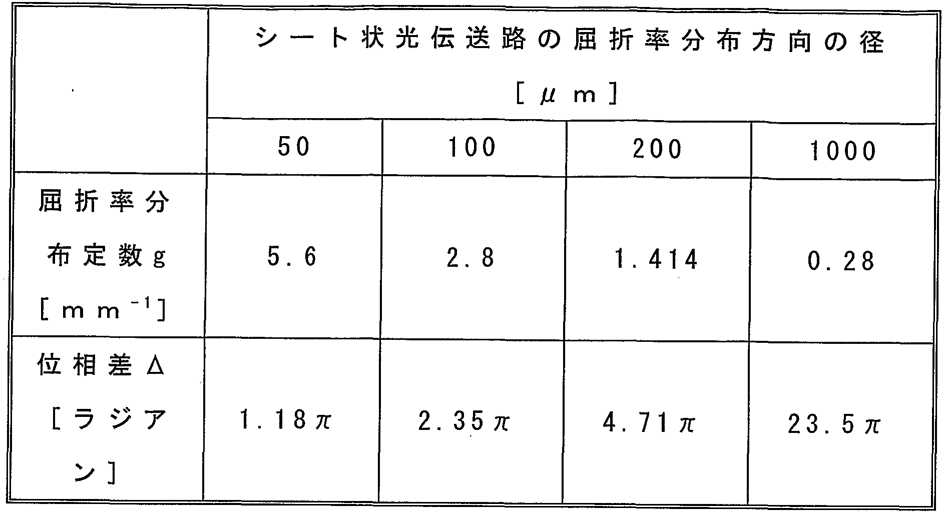

Claims
Priority Applications (5)
| Application Number | Priority Date | Filing Date | Title |
|---|---|---|---|
| JP2005506384A JP4130834B2 (ja) | 2003-05-23 | 2004-05-19 | 光デバイス及び光デバイスの製造方法、ならびに光集積デバイス |
| CN200480001705XA CN1723401B (zh) | 2003-05-23 | 2004-05-19 | 光器件和光器件制造方法以及光集成器件 |
| US10/534,835 US7266277B2 (en) | 2003-05-23 | 2004-05-19 | Optical device, optical device manufacturing method, and optical integrated device |
| EP04733957.7A EP1662284B1 (en) | 2003-05-23 | 2004-05-19 | Optical device, optical device manufacturing method, and optical integrated device |
| KR1020057010671A KR101228225B1 (ko) | 2003-05-23 | 2004-05-19 | 광디바이스, 광디바이스의 제조방법 및 광집적 디바이스 |
Applications Claiming Priority (6)
| Application Number | Priority Date | Filing Date | Title |
|---|---|---|---|
| JP2003-145708 | 2003-05-23 | ||
| JP2003145708 | 2003-05-23 | ||
| JP2004017655 | 2004-01-26 | ||
| JP2004-017655 | 2004-01-26 | ||
| JP2004068066 | 2004-03-10 | ||
| JP2004-068066 | 2004-03-10 |
Publications (1)
| Publication Number | Publication Date |
|---|---|
| WO2004104662A1 true WO2004104662A1 (ja) | 2004-12-02 |
Family
ID=33479646
Family Applications (1)
| Application Number | Title | Priority Date | Filing Date |
|---|---|---|---|
| PCT/JP2004/007136 WO2004104662A1 (ja) | 2003-05-23 | 2004-05-19 | 光デバイス及び光デバイスの製造方法、ならびに光集積デバイス |
Country Status (6)
| Country | Link |
|---|---|
| US (1) | US7266277B2 (ja) |
| EP (1) | EP1662284B1 (ja) |
| JP (1) | JP4130834B2 (ja) |
| KR (1) | KR101228225B1 (ja) |
| CN (1) | CN1723401B (ja) |
| WO (1) | WO2004104662A1 (ja) |
Cited By (3)
| Publication number | Priority date | Publication date | Assignee | Title |
|---|---|---|---|---|
| WO2012099275A1 (ja) * | 2011-01-21 | 2012-07-26 | 日本電気株式会社 | 光カプラと分岐制御方法 |
| JP2014006338A (ja) * | 2012-06-22 | 2014-01-16 | Ntt Electornics Corp | 光電子集積モジュール |
| CN103731210B (zh) * | 2013-12-30 | 2016-01-20 | 北京航空航天大学 | 一种用于ase光纤光源的多功能集成器件 |
Families Citing this family (22)
| Publication number | Priority date | Publication date | Assignee | Title |
|---|---|---|---|---|
| JP3768901B2 (ja) * | 2002-02-28 | 2006-04-19 | 松下電器産業株式会社 | 立体光導波路の製造方法 |
| JPWO2005114278A1 (ja) * | 2004-05-21 | 2008-03-27 | 松下電器産業株式会社 | 屈折率分布型光学部材、屈折率分布型光学部材の製造方法、光モジュール、および光モジュールの製造方法 |
| JP4556149B2 (ja) * | 2008-03-27 | 2010-10-06 | ソニー株式会社 | 指向特性取得方法及び指向特性取得装置 |
| DE102008044818A1 (de) * | 2008-08-28 | 2010-03-04 | Fraunhofer-Gesellschaft zur Förderung der angewandten Forschung e.V. | Multimode-Interferenzkoppler und Verfahren zu seiner konstruktiven Ausgestaltung |
| KR101627117B1 (ko) * | 2009-03-31 | 2016-06-13 | 셀렉스 이에스 에스.피.에이. | 2차 비선형 광 계수 결정 방법 및 시스템 |
| US8606058B2 (en) * | 2009-04-30 | 2013-12-10 | Hewlett-Packard Development Company, L.P. | Multi-channel optical coupler |
| JP5482346B2 (ja) * | 2010-03-18 | 2014-05-07 | 富士通株式会社 | 光導波路素子及びそのような光導波路素子を備えた光受信機 |
| KR101176950B1 (ko) * | 2010-09-17 | 2012-08-30 | 주식회사 유나이브 | 부품의 수동 정렬을 구현하는 광 송수신 장치 및 부품의 수동 정렬방법 |
| CN104025376B (zh) * | 2012-01-18 | 2016-10-26 | 索尼公司 | 传输线和传输方法 |
| WO2017022719A1 (ja) * | 2015-08-04 | 2017-02-09 | 旭硝子株式会社 | 樹脂光導波路 |
| US10094980B2 (en) * | 2016-01-12 | 2018-10-09 | King Saud University | Three-dimensional space-division Y-splitter for multicore optical fibers |
| US9864139B1 (en) * | 2016-01-22 | 2018-01-09 | Seagate Technology Llc | Uniform laser direct writing for waveguides |
| US10288808B1 (en) | 2016-01-22 | 2019-05-14 | Seagate Technology Llc | Laser direct writing for non-linear waveguides |
| JP6639696B2 (ja) * | 2016-11-10 | 2020-02-05 | 三菱電機株式会社 | 集積型光モジュールの光軸調整方法、製造方法、および光軸調整装置 |
| FR3061561B1 (fr) * | 2016-12-29 | 2019-05-31 | Commissariat A L'energie Atomique Et Aux Energies Alternatives | Dispositif de collimation |
| CN108983446B (zh) * | 2017-06-01 | 2021-04-06 | Tcl科技集团股份有限公司 | 一种光强调制器 |
| US11009662B2 (en) * | 2017-09-05 | 2021-05-18 | Facebook Technologies, Llc | Manufacturing a graded index profile for waveguide display applications |
| JP6716029B1 (ja) | 2018-10-10 | 2020-07-01 | 三菱電機株式会社 | 多モード干渉型光導波路デバイス及び光集積回路 |
| CN109239835A (zh) * | 2018-10-19 | 2019-01-18 | 成都理想境界科技有限公司 | 波导、成像扩展模组、光源模组、近眼显示系统及设备 |
| US11243365B2 (en) * | 2018-11-16 | 2022-02-08 | The Boeing Company | Methods for providing flammability protection for plastic optical fiber |
| RU199247U1 (ru) * | 2019-11-29 | 2020-08-24 | Федеральное государственное бюджетное образовательное учреждение высшего образования "Московский государственный университет имени М.В. Ломоносова" (МГУ) | Оптический интегральный чип с элементом для ввода излучения в волновод или вывода из него |
| CN110927969A (zh) * | 2019-12-09 | 2020-03-27 | 京东方科技集团股份有限公司 | 光学显示系统和显示装置 |
Citations (5)
| Publication number | Priority date | Publication date | Assignee | Title |
|---|---|---|---|---|
| US3614197A (en) * | 1967-04-27 | 1971-10-19 | Semiconductor Res Found | Solid optical wave guide having a radially varying refractive index |
| WO1992011550A1 (en) * | 1990-12-20 | 1992-07-09 | The Secretary Of State For Defence In Her Britannic Majesty's Government Of The United Kingdom Of Great Britain And Northern Ireland | Optical device |
| JPH1184434A (ja) * | 1997-09-02 | 1999-03-26 | Nippon Telegr & Teleph Corp <Ntt> | 光制御回路および動作方法 |
| JP2000111738A (ja) * | 1998-10-08 | 2000-04-21 | Fuji Xerox Co Ltd | 光データバス、光データバスの製造方法、および信号処理装置 |
| JP2001183710A (ja) * | 1999-12-27 | 2001-07-06 | Kddi Corp | 多モード干渉導波路型光スイッチ |
Family Cites Families (15)
| Publication number | Priority date | Publication date | Assignee | Title |
|---|---|---|---|---|
| FR2285623A1 (fr) | 1974-09-20 | 1976-04-16 | Max Planck Gesellschaft | Dispositif auto-formateur d'images, comportant un guide d'ondes |
| US4712854A (en) * | 1983-07-11 | 1987-12-15 | Omron Tateisi Electronics Co. | Optical waveguide and method of making the same |
| JPS6235304A (ja) | 1985-08-09 | 1987-02-16 | Nippon Telegr & Teleph Corp <Ntt> | レンズ付き光導波路回路及びその製造方法 |
| JPH01156703A (ja) | 1987-12-14 | 1989-06-20 | Fujitsu Ltd | 光カプラ |
| GB2220764B (en) | 1988-07-15 | 1992-02-19 | Stc Plc | Single mode couplers |
| JPH0511132A (ja) | 1991-07-08 | 1993-01-19 | Nippondenso Co Ltd | 光分岐結合器 |
| JPH08201648A (ja) | 1995-01-26 | 1996-08-09 | Nippon Telegr & Teleph Corp <Ntt> | 光導波回路 |
| JP3837980B2 (ja) | 1999-03-16 | 2006-10-25 | 富士ゼロックス株式会社 | 光分岐装置及びこれを用いた光バス回路 |
| JP3988357B2 (ja) | 1999-09-08 | 2007-10-10 | 富士ゼロックス株式会社 | 光バス回路基板 |
| US6836608B2 (en) * | 2000-12-28 | 2004-12-28 | Matsushita Electric Industrial Co., Ltd. | Planar optical waveguide, method for manufacturing the same and polymer optical waveguide |
| US7035518B2 (en) * | 2001-04-13 | 2006-04-25 | Hitachi Cable, Ltd. | Polymer waveguides and process for producing the same |
| JP2003043285A (ja) | 2001-07-27 | 2003-02-13 | Matsushita Electric Ind Co Ltd | 光デバイスの製造方法および光デバイス |
| AU2003224891A1 (en) * | 2002-04-09 | 2003-10-27 | Massachusetts Institute Of Technology | Polysilane thin films for directly patternable waveguides |
| JP2004012635A (ja) * | 2002-06-04 | 2004-01-15 | Nippon Paint Co Ltd | 光電気配線複合実装基板及びその製造方法 |
| CN1304861C (zh) * | 2002-06-27 | 2007-03-14 | 松下电器产业株式会社 | 光波导和用于制造该光波导的方法 |
-
2004
- 2004-05-19 CN CN200480001705XA patent/CN1723401B/zh not_active Expired - Fee Related
- 2004-05-19 US US10/534,835 patent/US7266277B2/en active Active
- 2004-05-19 EP EP04733957.7A patent/EP1662284B1/en not_active Expired - Fee Related
- 2004-05-19 JP JP2005506384A patent/JP4130834B2/ja not_active Expired - Fee Related
- 2004-05-19 WO PCT/JP2004/007136 patent/WO2004104662A1/ja active Application Filing
- 2004-05-19 KR KR1020057010671A patent/KR101228225B1/ko active IP Right Grant
Patent Citations (5)
| Publication number | Priority date | Publication date | Assignee | Title |
|---|---|---|---|---|
| US3614197A (en) * | 1967-04-27 | 1971-10-19 | Semiconductor Res Found | Solid optical wave guide having a radially varying refractive index |
| WO1992011550A1 (en) * | 1990-12-20 | 1992-07-09 | The Secretary Of State For Defence In Her Britannic Majesty's Government Of The United Kingdom Of Great Britain And Northern Ireland | Optical device |
| JPH1184434A (ja) * | 1997-09-02 | 1999-03-26 | Nippon Telegr & Teleph Corp <Ntt> | 光制御回路および動作方法 |
| JP2000111738A (ja) * | 1998-10-08 | 2000-04-21 | Fuji Xerox Co Ltd | 光データバス、光データバスの製造方法、および信号処理装置 |
| JP2001183710A (ja) * | 1999-12-27 | 2001-07-06 | Kddi Corp | 多モード干渉導波路型光スイッチ |
Non-Patent Citations (3)
| Title |
|---|
| LI B. ET AL: "Low-loss 1x2 multimode interference wavelength demultiplexer in silicon-germanium alloy", IEEE PHOTONICS TECHNOLOGY LETTERS, vol. 11, no. 5, May 1999 (1999-05-01), pages 575 - 577, XP000830418 * |
| LIN K-C. ET AL: "Guided-wave 1.3/1.55 mum wavelength division multiplexer based on multimode interference", ELECTRONICS LETTERS, vol. 32, no. 14, 4 July 1996 (1996-07-04), pages 1259 - 1261, XP006005373 * |
| SOLDANO L.B. ET AL: "Optical multi-mode interference devices based on self-imaging: principles and applications", J. OF LIGHTWAVE TECHNOLOGY, vol. 13, no. 4, April 1995 (1995-04-01), pages 615 - 627, XP000513578 * |
Cited By (4)
| Publication number | Priority date | Publication date | Assignee | Title |
|---|---|---|---|---|
| WO2012099275A1 (ja) * | 2011-01-21 | 2012-07-26 | 日本電気株式会社 | 光カプラと分岐制御方法 |
| JP2014006338A (ja) * | 2012-06-22 | 2014-01-16 | Ntt Electornics Corp | 光電子集積モジュール |
| US9229179B2 (en) | 2012-06-22 | 2016-01-05 | Ntt Electronics Corporation | Integrated optoelectronic module |
| CN103731210B (zh) * | 2013-12-30 | 2016-01-20 | 北京航空航天大学 | 一种用于ase光纤光源的多功能集成器件 |
Also Published As
| Publication number | Publication date |
|---|---|
| US7266277B2 (en) | 2007-09-04 |
| US20050259935A1 (en) | 2005-11-24 |
| KR101228225B1 (ko) | 2013-01-31 |
| CN1723401B (zh) | 2010-12-01 |
| EP1662284B1 (en) | 2015-03-25 |
| EP1662284A4 (en) | 2007-07-18 |
| JP4130834B2 (ja) | 2008-08-06 |
| CN1723401A (zh) | 2006-01-18 |
| EP1662284A1 (en) | 2006-05-31 |
| KR20060015453A (ko) | 2006-02-17 |
| JPWO2004104662A1 (ja) | 2006-07-20 |
Similar Documents
| Publication | Publication Date | Title |
|---|---|---|
| WO2004104662A1 (ja) | 光デバイス及び光デバイスの製造方法、ならびに光集積デバイス | |
| JP5259829B2 (ja) | 光結合装置及び光合分波装置 | |
| WO2016131355A1 (en) | Photonic chip surface grating coupler (sgc) -based optical splitter and optical combiner | |
| JP2010524022A (ja) | マルチプレクサ導波路結合方法およびシステム | |
| JP2000056146A (ja) | 自己導波光回路 | |
| WO2008035466A1 (fr) | Substrat de guide d'ondes optique et substrat supportant un circuit hybride photoélectrique | |
| JP2010044349A (ja) | 光波長合分波回路 | |
| JP2008250019A (ja) | 光集積回路および光集積回路モジュール | |
| JP6402519B2 (ja) | 光導波路素子 | |
| US20050013541A1 (en) | Diffraction device using photonic crystal | |
| JP2008261952A (ja) | 三次元交差導波路 | |
| WO2006051981A1 (ja) | 光反射器、光合分波器及び光システム | |
| KR101204335B1 (ko) | 배열 도파로 격자 구조체들을 구비하는 광 소자 칩 | |
| US20220146749A1 (en) | Self-Aligning Photonic Interconnections for Photonic Integrated Circuits | |
| JP6643437B1 (ja) | 光導波路素子 | |
| JP6530061B2 (ja) | グレーティングカプラ | |
| JP2023047302A (ja) | 多重化および逆多重化するマルチモードデバイス | |
| US11199659B2 (en) | Optical module | |
| Ura et al. | Integrated-optic free-space-wave coupler for package-level on-board optical interconnects | |
| Gruber et al. | Planar-integrated free-space optical fan-out module for MT-connected fiber ribbons | |
| US10061080B2 (en) | Multi-mode forked grating coupler | |
| JP2005010333A (ja) | 導波路型光信号処理器 | |
| JP5589066B2 (ja) | 光波をディジタル的に処理する方法およびディジタル平面ホログラフィに基づく集積平面光学装置 | |
| JP6335676B2 (ja) | 基板型光導波路素子 | |
| JP5291049B2 (ja) | 平面光波回路および受光デバイス |
Legal Events
| Date | Code | Title | Description |
|---|---|---|---|
| AK | Designated states |
Kind code of ref document: A1 Designated state(s): AE AG AL AM AT AU AZ BA BB BG BR BW BY BZ CA CH CN CO CR CU CZ DE DK DM DZ EC EE EG ES FI GB GD GE GH GM HR HU ID IL IN IS JP KE KG KP KR KZ LC LK LR LS LT LU LV MA MD MG MK MN MW MX MZ NA NI NO NZ OM PG PH PL PT RO RU SC SD SE SG SK SL SY TJ TM TN TR TT TZ UA UG US UZ VC VN YU ZA ZM ZW |
|
| AL | Designated countries for regional patents |
Kind code of ref document: A1 Designated state(s): BW GH GM KE LS MW MZ NA SD SL SZ TZ UG ZM ZW AM AZ BY KG KZ MD RU TJ TM AT BE BG CH CY CZ DE DK EE ES FI FR GB GR HU IE IT LU MC NL PL PT RO SE SI SK TR BF BJ CF CG CI CM GA GN GQ GW ML MR NE SN TD TG |
|
| 121 | Ep: the epo has been informed by wipo that ep was designated in this application | ||
| WWE | Wipo information: entry into national phase |
Ref document number: 10534835 Country of ref document: US |
|
| WWE | Wipo information: entry into national phase |
Ref document number: 2005506384 Country of ref document: JP |
|
| WWE | Wipo information: entry into national phase |
Ref document number: 2004733957 Country of ref document: EP |
|
| WWE | Wipo information: entry into national phase |
Ref document number: 1020057010671 Country of ref document: KR |
|
| WWE | Wipo information: entry into national phase |
Ref document number: 2004801705X Country of ref document: CN |
|
| WWP | Wipo information: published in national office |
Ref document number: 1020057010671 Country of ref document: KR |
|
| WWP | Wipo information: published in national office |
Ref document number: 2004733957 Country of ref document: EP |