WO2000040586A1 - Borane derivatives and organic electroluminescents - Google Patents
Borane derivatives and organic electroluminescents Download PDFInfo
- Publication number
- WO2000040586A1 WO2000040586A1 PCT/JP1999/007219 JP9907219W WO0040586A1 WO 2000040586 A1 WO2000040586 A1 WO 2000040586A1 JP 9907219 W JP9907219 W JP 9907219W WO 0040586 A1 WO0040586 A1 WO 0040586A1
- Authority
- WO
- WIPO (PCT)
- Prior art keywords
- group
- formula
- borane
- organic
- substituted
- Prior art date
- Legal status (The legal status is an assumption and is not a legal conclusion. Google has not performed a legal analysis and makes no representation as to the accuracy of the status listed.)
- Ceased
Links
Classifications
-
- C—CHEMISTRY; METALLURGY
- C07—ORGANIC CHEMISTRY
- C07F—ACYCLIC, CARBOCYCLIC OR HETEROCYCLIC COMPOUNDS CONTAINING ELEMENTS OTHER THAN CARBON, HYDROGEN, HALOGEN, OXYGEN, NITROGEN, SULFUR, SELENIUM OR TELLURIUM
- C07F5/00—Compounds containing elements of Groups 3 or 13 of the Periodic Table
- C07F5/02—Boron compounds
- C07F5/027—Organoboranes and organoborohydrides
-
- C—CHEMISTRY; METALLURGY
- C09—DYES; PAINTS; POLISHES; NATURAL RESINS; ADHESIVES; COMPOSITIONS NOT OTHERWISE PROVIDED FOR; APPLICATIONS OF MATERIALS NOT OTHERWISE PROVIDED FOR
- C09K—MATERIALS FOR MISCELLANEOUS APPLICATIONS, NOT PROVIDED FOR ELSEWHERE
- C09K11/00—Luminescent materials, e.g. electroluminescent or chemiluminescent
- C09K11/06—Luminescent materials, e.g. electroluminescent or chemiluminescent containing organic luminescent materials
-
- H—ELECTRICITY
- H10—SEMICONDUCTOR DEVICES; ELECTRIC SOLID-STATE DEVICES NOT OTHERWISE PROVIDED FOR
- H10K—ORGANIC ELECTRIC SOLID-STATE DEVICES
- H10K85/00—Organic materials used in the body or electrodes of devices covered by this subclass
- H10K85/30—Coordination compounds
- H10K85/321—Metal complexes comprising a group IIIA element, e.g. Tris (8-hydroxyquinoline) gallium [Gaq3]
- H10K85/322—Metal complexes comprising a group IIIA element, e.g. Tris (8-hydroxyquinoline) gallium [Gaq3] comprising boron
-
- H—ELECTRICITY
- H10—SEMICONDUCTOR DEVICES; ELECTRIC SOLID-STATE DEVICES NOT OTHERWISE PROVIDED FOR
- H10K—ORGANIC ELECTRIC SOLID-STATE DEVICES
- H10K85/00—Organic materials used in the body or electrodes of devices covered by this subclass
- H10K85/60—Organic compounds having low molecular weight
- H10K85/615—Polycyclic condensed aromatic hydrocarbons, e.g. anthracene
-
- H—ELECTRICITY
- H10—SEMICONDUCTOR DEVICES; ELECTRIC SOLID-STATE DEVICES NOT OTHERWISE PROVIDED FOR
- H10K—ORGANIC ELECTRIC SOLID-STATE DEVICES
- H10K85/00—Organic materials used in the body or electrodes of devices covered by this subclass
- H10K85/60—Organic compounds having low molecular weight
- H10K85/658—Organoboranes
-
- H—ELECTRICITY
- H10—SEMICONDUCTOR DEVICES; ELECTRIC SOLID-STATE DEVICES NOT OTHERWISE PROVIDED FOR
- H10K—ORGANIC ELECTRIC SOLID-STATE DEVICES
- H10K2102/00—Constructional details relating to the organic devices covered by this subclass
- H10K2102/10—Transparent electrodes, e.g. using graphene
- H10K2102/101—Transparent electrodes, e.g. using graphene comprising transparent conductive oxides [TCO]
- H10K2102/103—Transparent electrodes, e.g. using graphene comprising transparent conductive oxides [TCO] comprising indium oxides, e.g. ITO
-
- H—ELECTRICITY
- H10—SEMICONDUCTOR DEVICES; ELECTRIC SOLID-STATE DEVICES NOT OTHERWISE PROVIDED FOR
- H10K—ORGANIC ELECTRIC SOLID-STATE DEVICES
- H10K50/00—Organic light-emitting devices
- H10K50/10—OLEDs or polymer light-emitting diodes [PLED]
- H10K50/11—OLEDs or polymer light-emitting diodes [PLED] characterised by the electroluminescent [EL] layers
-
- H—ELECTRICITY
- H10—SEMICONDUCTOR DEVICES; ELECTRIC SOLID-STATE DEVICES NOT OTHERWISE PROVIDED FOR
- H10K—ORGANIC ELECTRIC SOLID-STATE DEVICES
- H10K85/00—Organic materials used in the body or electrodes of devices covered by this subclass
- H10K85/30—Coordination compounds
- H10K85/321—Metal complexes comprising a group IIIA element, e.g. Tris (8-hydroxyquinoline) gallium [Gaq3]
- H10K85/324—Metal complexes comprising a group IIIA element, e.g. Tris (8-hydroxyquinoline) gallium [Gaq3] comprising aluminium, e.g. Alq3
-
- H—ELECTRICITY
- H10—SEMICONDUCTOR DEVICES; ELECTRIC SOLID-STATE DEVICES NOT OTHERWISE PROVIDED FOR
- H10K—ORGANIC ELECTRIC SOLID-STATE DEVICES
- H10K85/00—Organic materials used in the body or electrodes of devices covered by this subclass
- H10K85/40—Organosilicon compounds, e.g. TIPS pentacene
-
- H—ELECTRICITY
- H10—SEMICONDUCTOR DEVICES; ELECTRIC SOLID-STATE DEVICES NOT OTHERWISE PROVIDED FOR
- H10K—ORGANIC ELECTRIC SOLID-STATE DEVICES
- H10K85/00—Organic materials used in the body or electrodes of devices covered by this subclass
- H10K85/60—Organic compounds having low molecular weight
- H10K85/631—Amine compounds having at least two aryl rest on at least one amine-nitrogen atom, e.g. triphenylamine
- H10K85/633—Amine compounds having at least two aryl rest on at least one amine-nitrogen atom, e.g. triphenylamine comprising polycyclic condensed aromatic hydrocarbons as substituents on the nitrogen atom
-
- Y—GENERAL TAGGING OF NEW TECHNOLOGICAL DEVELOPMENTS; GENERAL TAGGING OF CROSS-SECTIONAL TECHNOLOGIES SPANNING OVER SEVERAL SECTIONS OF THE IPC; TECHNICAL SUBJECTS COVERED BY FORMER USPC CROSS-REFERENCE ART COLLECTIONS [XRACs] AND DIGESTS
- Y10—TECHNICAL SUBJECTS COVERED BY FORMER USPC
- Y10S—TECHNICAL SUBJECTS COVERED BY FORMER USPC CROSS-REFERENCE ART COLLECTIONS [XRACs] AND DIGESTS
- Y10S428/00—Stock material or miscellaneous articles
- Y10S428/917—Electroluminescent
Definitions
- the present invention relates to a novel borane derivative, various materials using the borane derivative, and an organic electroluminescent device (hereinafter, referred to as an organic EL device). More specifically, the present invention relates to borane derivatives having a novel structure, various materials using a porane derivative having a structure useful for applications such as electronic functional materials and optical functional materials, and organic EL devices.
- an organic EL device an organic electroluminescent device
- borane compounds containing boron atoms in their molecules are expected to exhibit unique optical and electronic properties due to the existence of empty ⁇ orbitals of boron atoms.
- borane compounds generally have the drawback of being unstable to air and water, and thus are not suitable for use as materials.
- Document 4 also describes the physical properties of a fluorescent substance in a solution state, but does not describe luminescence in a solid state, nor does it describe application to a luminescent material.
- An organic EL device basically has a structure in which a charge transporting material or an organic compound serving as a luminescent material is sandwiched between two electrodes. It is desirable that the organic EL device has low power consumption and high efficiency, and for that purpose, it is necessary to use an organic compound which is a luminescent material having high luminous efficiency.
- Japanese Patent Application Laid-Open No. 7-102251 also discloses an example in which a boron compound is used for an organic or EL device.
- the boron compound used here had a high driving voltage and a low light emission luminance.
- the present inventors have conducted intensive studies to solve the problem of providing a novel borane derivative, various materials using the borane derivative, and an organic EL device, and as a result, have obtained a porane derivative having a specific structure and a specific structure.
- the present inventors have found that the above problems can be solved by using a borane derivative as a material, particularly in an organic EL device, and have completed the present invention.
- the borane derivative of the present invention is a novel compound represented by the following formula (1).
- the borane derivative of the present invention can be expected to be widely applied not only to light-emitting materials and charge-transporting materials but also to electronic functional materials and optical functional materials utilizing electronic properties derived from borane atoms. Things.
- 1 1 to 1 8 Oyopi 2 2 are each independently a hydrogen atom, a saturated or unsaturated hydrocarbon group, an aromatic group, a heterocyclic group, a substituted amino group, a substituted boryl group, an alkoxy X, Y and Zi each independently represent a saturated or unsaturated hydrocarbon group, an aromatic group, a heterocyclic group, a substituted amino group, an alkoxy group or an aryloxy group;
- the substituents of Z 2 and Z 2 may combine with each other to form a condensed ring, and n represents an integer of 1 to 3, and when n is 2 or more, Z i may be different.
- n is 1, X, Y and R 2 are methyl groups, and R s Does not include the case where is a hydrogen atom or a substituted boryl group, and the case where n is 3 and Z 1 is a methyl group.
- borane derivatives represented by the formula (1) those in which at least one substituted or unsubstituted 9-anthryl group is bonded to a boron atom are preferable.
- borane derivative of the present invention include compounds represented by the following formulas (3) to (9).
- the compound of the formula (3) is a borane derivative in which n is 3, R 4 R is a hydrogen atom, and ⁇ and Z s are benzo-condensed in the above formula (1).
- the compound of the formula (5) is a compound of the above formula (1), wherein R 4 to R 7 are a hydrogen atom, R 8 is a phenyl group, n is 3, and Z, and Z 2 are benzo-condensed borane. It is a derivative.
- n 2
- R 1 and R 3 to R 8 are hydrogen atoms
- R 2 , X and Y are methyl groups
- Z i and Z 2 are all It is a borane derivative obtained by azo condensation.
- n is 2
- RJ and R 3 to R 7 are a hydrogen atom
- R 2 , X and Y are a methyl group
- one of R 8 is an anthryl mesitylporyl group
- the remaining one of R 8 is a hydrogen atom, and the borane derivative obtained by benzo-condensation of Z 2 .
- n 3
- R 4 to R 8 are a hydrogen atom
- Z 2 is subjected to benzo-condensation at one place, and the remaining uncondensed 2
- One Z is a methyl group
- the other two non-condensed Z are borane derivatives of a hydrogen atom.
- n is 1, R 3 to R 7 are a hydrogen atom, R 2 , X and Y are methyl groups, R 8 is a phenyl group, ⁇ and Zeta 2 and is benzofused borane derivatives.
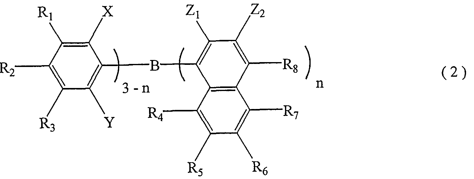
- the borane derivative used in the various materials of the present invention that is, the light emitting material, the charge transport material, and the organic EL device-related materials (light emitting layer, charge transport layer) is represented by the following formula (2).
- Ri Rg and Z 2 each independently represent a hydrogen atom, a saturated or unsaturated hydrocarbon group, an aromatic group, a heterocyclic group, a substituted amino group, a substituted boryl group, an alkoxy group or an aryloxy group.
- the borane derivative is preferably bulky in order to be stable even in the air and have sufficient durability and performance as a material, and has an anthracene ring and / or a naphthalene ring. It is desirable.
- At least one substituted or unsubstituted 9-anthryl of the borane derivative represented by the above formula (2) is included in the light emitting material, the charge transport material and the organic EL device of the present invention. Those having attached groups are preferred.
- borane derivatives include the compounds represented by the above formulas (3) to (9) and the compounds represented by the following formulas (10) to (14).
- the borane derivative of the present invention and the borane derivative used for various materials of the present invention can be synthesized by a known method represented by the following production method. it can. That is, the compound can be synthesized by reacting a compound represented by the general formula (15) with a base, followed by reacting with a borane compound.
- Ar represents the following formula (16) or (17), and W represents a halogen atom.
- R 1 to R 3 each independently represent a hydrogen atom, a saturated or unsaturated hydrocarbon group, an aromatic group, a heterocyclic group, a substituted amino group, a substituted boryl group, an alkoxy group, or an aryloxy group.
- X and Y each independently represent a saturated or unsaturated hydrocarbon group, an aromatic group, a heterocyclic group, a substituted amino group, an alkoxy group or an aryloxy group.
- Oyobi 2 2 are each independently a hydrogen atom, a saturated or unsaturated hydrocarbon group, an aromatic group, a heterocyclic group, a substituted amino group, a substituted boryl group, an alkoxy Z represents a saturated or unsaturated hydrocarbon group, an aromatic group, a heterocyclic group, a substituted amino group, an alkoxy group or an aryloxy group, and the substituents of Z i and Z 2 represent
- the base used in this production method may be, for example, an organic lithium reagent such as n-butyllithium, tert-butyllithium, or phenyllithium, magnesium, or magnesium bromide. And the like.
- the solvent used is not particularly limited as long as it is inert to these bases.
- Ether solvents such as getyl ether or tetrahydrofuran (hereinafter referred to as THF) or aromatic solvents such as benzene and toluene are used.
- examples of the borane compound to be used include halogenated borane such as trichloroborane, trifluoroborane or a complex thereof, and alkoxyborane such as trimethoxyborane or trisopropoxyborane.
- reaction temperature is not particularly limited, but is usually preferably about 178 ° C to 120 ° C.
- reaction time There is no particular limitation on the reaction time for these reactions, and the reaction may be stopped when the reaction has sufficiently proceeded.
- the reaction may be tracked by a general analytical means such as NMR or chromatography, and the end point of the reaction may be determined at an optimum time.
- the borane derivative of the present invention can also be obtained by subjecting the obtained compound to a substitution reaction.
- Substituents added by the substitution reaction include methyl, ethyl, normal propyl, isopropyl, cyclopentyl, tert-butyl and other alkyl groups, vinyl groups, aryl groups, butyr groups, and styryl groups.
- Amino groups such as alkenyl groups, methoxy groups, ethoxy groups, propoxy groups, phenyloxy groups, etc.
- aryloxy groups dimethylamino groups, diphenylamino groups, etc., trimethylsilyl groups, dimethyl-tert-butylsilyl groups, trimethoxysilyl groups and Silyl groups such as triunylsilyl group, boryl groups such as dianthyl boryl group, dimesityl boryl group, phenyl group, naphthyl group, anthryl group, biphenyl group, tolyl group, pyrenyl group, perylenyl group, anisyl group, turf Aryl groups such as phenyl and phenanthrenyl groups; And heterocyclic rings such as a phenanthrolyl group, a benzochenyl group, a benzothiazolyl group, an indolyl group, a silacyclopentagenenyl group and a pyridyl group.
- boryl groups such as dianthyl boryl group, dimesityl boryl group, phenyl group,
- the organic EL device of the present invention basically has a structure in which a borane derivative layer containing a borane derivative represented by the above formula (2) as a main component is sandwiched between a pair of electrodes and (anode and cathode). Things.
- the borane derivative can be used as both a light emitting material and a charge transport material, it is suitable as a material for a light emitting layer and a charge transport layer (a hole injection layer, a hole transport layer, an electron injection layer, and an electron transport layer).
- the obtained borane derivative layer effectively functions as a light emitting layer and a charge transport layer.
- a hole injection material, a hole transport material, a light emitting material, an electron injection material, an electron transport material, or the like other than the borane derivative may be added to the borane derivative layer.
- an electron-donating compound and an electron-accepting compound serving as a charge transporting material are often used, and a mixture thereof is added or these are laminated and used. However, they are also known to form undesirable charge transfer complexes or exciplexes.
- the borane derivative used in the present invention since the bulky group bonded to the boron atom is arranged in a propeller shape centering on the boron atom, it is difficult to form a charge transfer complex or an exciplex. It has a structure. Accordingly, when the borane derivative is used as a material for an organic EL device as an electron donating compound or an electron accepting compound, there is an advantage that a highly efficient device can be easily obtained.
- a hole injection layer, a hole transport layer, a light emitting layer, an electron injection layer, an electron transport layer, an interface layer, and the like may be arbitrarily provided between the electrodes in addition to the borane derivative layer. No problem.
- the hole injection layer, the electron injection layer, the hole transport layer, the electron transport layer, and the interface layer are not necessarily required, but by providing these layers, the luminous efficiency can be improved.
- the introduction of a hole injection layer and a hole transport layer greatly improves luminous efficiency.
- the organic EL device of the present invention is preferably supported on a substrate.
- the substrate only needs to have mechanical strength, thermal stability and transparency, and glass, a transparent plastic film, or the like can be used.
- anode material used for the anode of the organic EL device of the present invention metals, alloys, electrically conductive compounds having a work function greater than 4 eV, and mixtures thereof can be used.
- a metal such as A u, C ul, indium tin O hexa Lee de (hereinafter, referred to as ITO), S N_ ⁇ 2, a conductive transparent material such as Z eta theta is like et be.
- cathode material used for the cathode of the organic EL device of the present invention metals, alloys, electrically conductive compounds, and mixtures thereof having a work function smaller than 4 eV can be used.
- specific examples include calcium, magnesium, lithium, aluminum, magnesium alloys, lithium alloys, aluminum alloys, and the like, and mixtures thereof include aluminum lithium, magnesium / silver, magnesium / indium, and the like.
- the electrodes has a light transmittance of at least 10% in order to efficiently extract light emitted from the organic EL element.
- the sheet resistance as an electrode is preferably several hundred ⁇ or less.
- the film thickness depends on the properties of the electrode material, and is usually selected from the range of 10 nm to 1 ⁇ , preferably 10 to 400 nm.
- Such an electrode can be manufactured by forming a thin film by a method such as vapor deposition and sputtering using the above-mentioned electrode materials (anode material and cathode material).
- the light-emitting layer which is an essential constituent layer of the organic EL device of the present invention, has the formula (2)
- a borane derivative is preferably used, a light-emitting material other than the borane derivative may be used. Further, by using a mixture of the borane derivative represented by the formula (2) and a light emitting material other than the borane derivative, light having a wavelength different from that of the borane derivative can be generated, and the luminous efficiency can be further improved. It should be noted that there is no problem in using two or more borane derivatives represented by the formula (2) in combination.
- Such luminescent materials other than the borane derivative represented by the formula (2) include the luminescent materials described in “Polyfunctional Materials” edited by the Society of Polymer Science, “Optical Functional Materials”, Kyoritsu Shuppan (1991), p.236. Known substances such as photofluorescent materials, fluorescent brighteners, laser dyes, organic scintillators, and various fluorescent analysis reagents can be mentioned.
- polycyclic condensed compounds such as anthracene, phenanthrene, pyrene, chrysene, perylene, coronene, rubrene, and quinatalidone; oligophenylene compounds such as quarter phenyl; 1,4-bis (2-methylstyrinole) benzene 1,4-bis (4-methylstyryl) benzene, 1,4-bis (4-methyl-5-phenyl-2-oxazolyl) benzene, 1,4-bis (5-phenyl-2-oxazolyl) benzene , 2,5-bis (5- tert-butyl-2-benzoxazolyl) thiophene, 1,4-diphenyl-1,3-phenyl "thagene, 1,6-diphenyl-1,3,5- Hexatriene, scintillator for liquid scintillation such as 1,1,4,4-tetraphenyl-1,3-butadiene,
- the hole injection layer which is a selective component layer of the organic EL device of the present invention, can be obtained by using a hole injection material.
- a hole injection material In this case, one or more hole injection materials are used to form a single hole injection layer.
- An injection layer may be obtained, and a plurality of hole injection layers may be obtained using several different hole injection materials.
- the hole transporting layer which is a selective component layer of the organic EL device of the present invention, comprises a hole transporting material.
- one hole transport layer may be obtained using one or more hole transport materials, and a plurality of hole transport layers may be obtained using several different types of hole transport materials.
- a hole transport layer may be obtained.
- a borane derivative represented by the above formula (2) can be used as the hole injection material and the hole transport material.
- any known substance that can be used for the hole injection layer and the hole transport layer of the organic EL device include, for example, carbazole derivatives (N-phenylcarbazole, polybutyl carbazole, etc.), triarylamine derivatives (TPD, polymers having an aromatic tertiary amine in the main chain or side chain).
- NPD 1,1-bis (4-di-p-tolylaminophenyl) cyclohexane, ⁇ , ⁇ '-diphenyl-N, ⁇ '-dinaphthyl-4,4'-diaminobiphenyl (hereinafter abbreviated as NPD) ), 4, 4 ', 4 "-tris ⁇ - (3-methylphenyl) - ⁇ -phenylamino) triphenylamine, Journal of the' Chemical Society Society Chemical Communication No. 2175 page 1996 Compounds described in Japanese Patent Application Laid-Open Nos.
- JP-A No. 8-100172 and JP-A-8-48656 such as starburst amine derivatives described in Advanced Materials, Vol. 6, page 677 (1994), stilbenes, etc. Derivatives (Chemical Society of Japan 72nd Annual Meeting Preprints (11), p. 1392, pp. 29898, etc.), phthalocyanine derivatives (metal-free, copper phthalocyanine, etc.), polysilanes, and the like.
- the electron injection layer which is a selective constituent layer of the organic EL device of the present invention, can be obtained by using an electron injection material.
- one or more electron injection materials are used to obtain one electron injection layer.
- the electron transport layer which is a selective component layer of the organic EL device of the present invention, can be obtained by using an electron transport material.
- one or more electron transport materials are used to form one electron transport layer.
- Layers may be obtained, and a plurality of electron transport layers may be obtained using several different types of electron transport materials.
- the electron injection material and the electron transport material it is preferable to use a borane derivative represented by the above formula (2), but in photoconductive materials, those conventionally used as electron transfer compounds, Any known substance that can be used for the electron injection layer and the electron transport layer of the organic EL element can be selected and used.
- Examples of such known materials include, for example, Jifuwe two Rukinon derivative (electrophotographic Journal, 30,3 (1991) as described in, etc.), Peri Ren derivative (J.Apply.Phys., 2 ⁇ , 2 6 9 (1988)), oxadiazole derivatives (Jpn. J. Appl. Phys., 27, L713 (1988), Applied 'Physics' Letter (Appl. Phys. Lett.), 55, 1 489 (1989), such as those described in), such as those described in Chiofen derivative (JP-a-4 one 2 1 2286 JP), Toriazoru derivative (Jpn.
- the hole injecting material, hole transporting material, light emitting material, electron injecting material and the like which can be used in the organic EL device of the present invention preferably have a T g of 80 ° C. or higher, more preferably a T g of 80 ° C. or higher. More than 100 ° C.
- the interface layer which is a selective constituent layer of the organic EL device of the present invention, is preferably a layer capable of promoting the injection of electrons from the cathode, and a layer capable of preventing holes from flowing into the cathode. These are selected depending on the compatibility with the material used for the cathode, and specific examples thereof include lithium fluoride, magnesium fluoride, calcium fluoride, and the like.
- Each layer constituting the organic EL device of the present invention can be formed by forming a material constituting each layer into a thin film by a known method such as an evaporation method, a spin coating method, and a casting method.
- each layer formed in this way is not particularly limited, and can be appropriately selected according to the properties of the material. It is selected within the range of ⁇ 500 nm.
- the vapor deposition conditions vary depending on the type of the borane derivative, the target crystal structure and the association structure of the molecule-cumulative film, but generally, the boat heating temperature is 50 to 400 ° C. , vacuum 1 0- 6 ⁇ :. 1 0- 3 P a, the deposition rate 0 0 1 ⁇ 5 O n mZ seconds, the substrate temperature one 1 5 0 tens 3 0 0 ° C, film thickness 5 eta [pi! It is desirable to select an appropriate value within the range of 5 ⁇ m.
- an organic EL device of the present invention a method for producing an organic EL device having the above-mentioned constitution (1) and comprising the anode Z-borane derivative layer / cathode will be described.
- the anode After forming a thin film made of an anode material on a suitable substrate by a vapor deposition method so as to have a film thickness of preferably in the range of 10 to 200 nm, the anode is formed.
- a borane derivative thin film is formed thereon to form a light emitting layer, and a thin film made of a cathode material is formed on the light emitting layer to a thickness of 1 ⁇ m or less by vapor deposition to form a cathode.
- the organic EL device of (1) is obtained.
- the production order can be reversed, and the cathode, the light emitting layer, and the anode can be produced in this order.
- the anode When a DC voltage is applied to the organic EL device obtained in this manner, the anode may be applied with + polarity and the cathode may be applied with one polarity. Light emission can be observed from the transparent electrode side (anode or cathode, and both).
- the organic EL element also emits light when an AC voltage is applied.
- the waveform of the applied AC may be arbitrary.
- Example 2 The synthesis was carried out in the same manner as in Example 1, except that 9,10-dilithioanthracene used in Example 1 was changed to mesityl lithium.
- a transparent support substrate was prepared by depositing ITO to a thickness of 100 nm on a glass substrate of 25 mmX 75 mmX 1.1 mm by an evaporation method (manufactured by Tokyo Sanyo Vacuum Co., Ltd.). This transparent support substrate is fixed to a substrate holder of a commercially available vapor deposition device (manufactured by Vacuum Equipment Co., Ltd.), and N, N, dinaphthyl ⁇ , ⁇ '-diphenylbenzidine (hereinafter abbreviated as NPD) is added.
- a quartz crucible containing 4-diphenylsilacyclopentadiene (hereinafter referred to as ⁇ ), a graphite crucible containing magnesium, and a Daraphite crucible containing silver were installed.
- Pressure of the vacuum vessel was reduced to 1 X 10- 3 P a, and heating the crucible NPD containing, by depositing NPD to a film thickness of 5 0 nm to form a hole transport layer, then the above formula
- the crucible containing the compound represented by (10) is heated and vapor-deposited to a thickness of 15 nm to form a light-emitting layer.
- the crucible containing PYPY is heated to form a film.
- An electron transporting layer was formed by vapor-depositing ⁇ to have a thickness of 35 ⁇ m.
- the deposition rate was between 0.1 and 0.211111 ns.
- the I TO electrodes anode, a cathode an alloy electrode of magnesium and silver, the indicia pressurizing a DC voltage of about 1 m AZ cm 2 of current flows, the luminance of about 100 cd / m 2, wavelength 51
- a device was prepared in the same manner as in Example 4, except that the compound represented by the formula (10) was replaced with tris (8-hydroxyquinoline).
- a device was prepared in the same manner as in Example 4 except that the compound represented by the above formula (10) was changed to trimesityl borane.
- a device was prepared in the same manner as in Example 4 except that the thickness of the layer made of the compound represented by the formula (10) was changed to 5 O nm without using PYPY used in Example 4.
- the I tO electrodes an anode, a cathode an alloy electrode of magnesium and silver, the indicia pressurizing a DC voltage of about 1 mA / cm 2 current flows, brightness of about 6 cd / m 2, wavelength 5 1 5 eta m A green luminescence was obtained.
- a device was prepared in the same manner as in Example 4, except that the compound represented by the formula (10) used in Example 4 was replaced with the compound represented by the formula (4).
- a device was prepared in the same manner as in Example 4, except that the compound represented by the formula (10) used in Example 4 was replaced with the compound represented by the formula (11).
- the I TO electrodes anode, a cathode an alloy electrode of magnesium and silver, the indicia pressurizing a DC voltage of about 1 mA / cm 2 current flows, the luminance of about 3 0 c dZm 2, blue light emission wavelength 464 nm Obtained.
- the transparent supporting substrate used in Example 4 was fixed to a substrate holder of a vapor deposition apparatus and a quartz crucible containing NPD, a quartz crucible containing a compound represented by the formula (10), and a tungsten crucible containing aluminum A crucible made of tundane and a crucible made of tundatin containing lithium fluoride were attached.
- Pressure of the vacuum vessel was reduced to 1 X 1 0- 3 P a, and heating the crucible NPD containing, by depositing NPD to a film thickness of 5 0 nm to form a hole transport layer, then the formula ( The crucible containing the compound represented by (10) was heated and evaporated to a thickness of 50 nm to form an electron-transporting luminescent layer. The deposition rate was between 0.1 and 0.2 nm / sec. Then pressure of the vacuum vessel was reduced to 2 X 1 0- 4 P a, heated tungsten crucible was deposited lithium fluoride on the 2 nm organic layer, and finally aluminum was 1 00 nm deposited, organic An EL device was obtained.
- a device was prepared in the same manner as in Example 8, except that the compound represented by the formula (10) used in Example 8 was changed to a compound represented by the formula (4).
- the I TO electrodes anode, a cathode an alloy electrode of magnesium and silver, the indicia pressurizing the DC voltage, the current flows of about 2 mA / cm 2, the luminance of about 1 5 cd / m 2, wavelength 6 1 6
- a device was prepared in the same manner as in Example 4, except that the compound represented by the formula (10) used in Example 4 was replaced with the compound represented by the formula (9).
- a device was prepared in the same manner as in Example 4, except that the compound represented by the formula (10) used in Example 4 was replaced with the compound represented by the formula (12).
- the I TO electrodes anode, a cathode an alloy electrode of magnesium and silver, the indicia pressurizing a DC voltage, from about 0. ⁇ ⁇ / C m 2 of current flows, the luminance of about 1 0 0 cd / m 2, wavelength of 5 1 A green emission of 1 nm was obtained.
- a device was prepared in the same manner as in Example 4, except that the compound represented by the formula (10) used in Example 4 was replaced with the compound represented by the formula (13).
- the transparent supporting substrate used in Example 4 was fixed to a substrate holder of a vapor deposition apparatus, and a quartz crucible containing an NPD, a quartz crucible containing a compound represented by the formula (10), and a quartz crucible represented by the formula (11)
- a quartz crucible containing a compound, a quartz crucible containing PYP Y, a tungsten crucible containing aluminum, and a tungsten crucible containing lithium fluoride were attached.
- Example 13 The compound represented by the formula (10) used in Example 13 was added to the compound represented by the formula (14), and the compound represented by the formula (11) was added to tris 8-hydroxyquinoline aluminum.
- An element was prepared in the same manner as in Example 13 except that the element was changed to a yum.
- the borane derivative which is a novel compound of the present invention, has high luminous efficiency in a solid state, and thus is suitable as a luminescent material. It is also useful as optoelectronic functional materials such as electrophotography, nonlinear optical materials, and conductive materials.
- the organic EL device of the present invention uses a luminescent material having high luminous efficiency, a display with low power consumption and a long life can be produced by using the luminescent material.
Landscapes
- Chemical & Material Sciences (AREA)
- Engineering & Computer Science (AREA)
- Materials Engineering (AREA)
- Organic Chemistry (AREA)
- Physics & Mathematics (AREA)
- Spectroscopy & Molecular Physics (AREA)
- Inorganic Chemistry (AREA)
- Electroluminescent Light Sources (AREA)
Description


Claims

Priority Applications (4)
| Application Number | Priority Date | Filing Date | Title |
|---|---|---|---|
| EP99961319A EP1142895B1 (en) | 1999-01-08 | 1999-12-22 | Borane derivatives and organic electroluminescents |
| DE69932263T DE69932263T2 (de) | 1999-01-08 | 1999-12-22 | Borderivate und organische elektrolumineszierende verbindungen |
| US09/869,920 US6767654B2 (en) | 1999-01-08 | 1999-12-22 | Organic electroluminescent device |
| JP2000592294A JP4055363B2 (ja) | 1999-01-08 | 1999-12-22 | ボラン誘導体および有機電界発光素子 |
Applications Claiming Priority (2)
| Application Number | Priority Date | Filing Date | Title |
|---|---|---|---|
| JP278699 | 1999-01-08 | ||
| JP11/2786 | 1999-01-08 |
Publications (1)
| Publication Number | Publication Date |
|---|---|
| WO2000040586A1 true WO2000040586A1 (en) | 2000-07-13 |
Family
ID=11539046
Family Applications (1)
| Application Number | Title | Priority Date | Filing Date |
|---|---|---|---|
| PCT/JP1999/007219 Ceased WO2000040586A1 (en) | 1999-01-08 | 1999-12-22 | Borane derivatives and organic electroluminescents |
Country Status (5)
| Country | Link |
|---|---|
| US (1) | US6767654B2 (ja) |
| EP (1) | EP1142895B1 (ja) |
| JP (1) | JP4055363B2 (ja) |
| DE (1) | DE69932263T2 (ja) |
| WO (1) | WO2000040586A1 (ja) |
Cited By (28)
| Publication number | Priority date | Publication date | Assignee | Title |
|---|---|---|---|---|
| EP1217668A1 (de) * | 2000-12-22 | 2002-06-26 | Covion Organic Semiconductors GmbH | Verwendung von Bor- und Aluminium-Verbindungen in Elektronik-Bauteilen |
| JP2003031367A (ja) * | 2001-07-11 | 2003-01-31 | Konica Corp | 有機エレクトロルミネッセンス素子及び表示装置 |
| JP2003031368A (ja) * | 2001-07-11 | 2003-01-31 | Konica Corp | 有機エレクトロルミネッセンス素子及び表示装置 |
| JP2003208988A (ja) * | 2001-11-09 | 2003-07-25 | Konica Corp | 有機エレクトロルミネッセンス素子及び表示装置 |
| JP3440296B2 (ja) | 1999-09-02 | 2003-08-25 | 大阪大学長 | エレクトロルミネッセンス素子 |
| WO2005039246A1 (ja) * | 2003-09-30 | 2005-04-28 | Konica Minolta Holdings, Inc. | 有機エレクトロルミネッセンス素子、照明装置、表示装置 |
| JP2005200638A (ja) * | 2003-12-19 | 2005-07-28 | Showa Denko Kk | ホウ素を含有する高分子化合物およびこれを用いた有機発光素子 |
| WO2005091686A1 (ja) * | 2004-03-19 | 2005-09-29 | Chisso Corporation | 有機電界発光素子 |
| WO2005104627A1 (ja) * | 2004-04-19 | 2005-11-03 | Idemitsu Kosan Co., Ltd. | 有機エレクトロルミネッセンス素子 |
| JP2006525395A (ja) * | 2003-05-08 | 2006-11-09 | オスラム オプト セミコンダクターズ ゲゼルシャフト ミット ベシュレンクテル ハフツング | 非共役のポリマーのペルアリール化ボラン、有機半導体発光材料及び/又は輸送材料としてのその使用、その製造方法及びその使用 |
| JP2007522271A (ja) * | 2003-12-29 | 2007-08-09 | オスラム オプト セミコンダクターズ ゲゼルシャフト ミット ベシュレンクテル ハフツング | 過アリール化ボランをベースとする、ポリマー燐光性有機半導体エミッター物質、その製法及びその使用 |
| JP2007531993A (ja) * | 2004-03-31 | 2007-11-08 | オスラム オプト セミコンダクターズ ゲゼルシャフト ミット ベシュレンクテル ハフツング | 有機発光ダイオード、並びにその使用 |
| WO2007145136A1 (ja) | 2006-06-15 | 2007-12-21 | Toray Industries, Inc. | 発光素子材料および発光素子 |
| JP2008227512A (ja) * | 2001-12-06 | 2008-09-25 | Konica Minolta Holdings Inc | 有機エレクトロルミネッセンス素子および表示装置 |
| JP2009507385A (ja) * | 2005-09-05 | 2009-02-19 | オスラム オプト セミコンダクターズ ゲゼルシャフト ミット ベシュレンクテル ハフツング | 有機電子素子における電子輸送層のn型ドーピングのための材料 |
| US7510782B2 (en) | 2003-12-19 | 2009-03-31 | Showa Denko K.K. | Boron-containing polymer compound and organic light emitting device using the same |
| US7737162B2 (en) | 2002-07-03 | 2010-06-15 | Gilead Sciences, Inc. | Viral inhibitors |
| JP2011049163A (ja) * | 2009-07-31 | 2011-03-10 | Fujifilm Corp | 有機電界発光素子用材料入り容器、並びに、有機電界発光素子用材料、蒸着膜及びその製造方法、有機電界発光素子、及び容器のスクリーニング方法 |
| JP2011151407A (ja) * | 2011-03-17 | 2011-08-04 | Konica Minolta Holdings Inc | 有機エレクトロルミネッセンス素子及び表示装置 |
| US8120022B2 (en) | 2007-07-27 | 2012-02-21 | Toray Industries, Inc. | Light emitting device material and light emitting device |
| WO2012102333A1 (ja) | 2011-01-27 | 2012-08-02 | Jnc株式会社 | 新規アントラセン化合物およびこれを用いた有機電界発光素子 |
| WO2013031638A1 (ja) * | 2011-08-31 | 2013-03-07 | 住友化学株式会社 | ボラン化合物と共役高分子化合物とを含む組成物及び素子 |
| WO2013077141A1 (ja) | 2011-11-25 | 2013-05-30 | Jnc株式会社 | ベンゾフルオレン化合物、該化合物を用いた発光層用材料および有機電界発光素子 |
| WO2014042197A1 (ja) | 2012-09-11 | 2014-03-20 | Jnc株式会社 | 有機電界発光素子用材料、有機電界発光素子、表示装置、及び照明装置 |
| US8686628B2 (en) | 2005-09-02 | 2014-04-01 | Semiconductor Energy Laboratory Co., Ltd. | Anthracene derivative |
| WO2015102118A1 (ja) | 2014-02-18 | 2015-07-09 | 学校法人関西学院 | 多環芳香族化合物 |
| WO2017055263A1 (en) | 2015-09-28 | 2017-04-06 | Novaled Gmbh | Organic electroluminescent devices comprising borane compounds |
| WO2018212169A1 (ja) | 2017-05-16 | 2018-11-22 | 学校法人関西学院 | 多環芳香族化合物 |
Families Citing this family (20)
| Publication number | Priority date | Publication date | Assignee | Title |
|---|---|---|---|---|
| KR101102102B1 (ko) | 2003-05-08 | 2012-01-18 | 오스람 옵토 세미컨덕터스 게엠베하 | 비콘쥬게이트된 중합성 퍼아릴화된 보란, 유기 반도체 트랜스미터 및/또는 운반 재료로서의 상기 보란의 용도, 상기 보란의 제조 방법 및 상기 방법의 적용 |
| DK2161273T3 (en) * | 2003-12-22 | 2015-07-20 | Leuven K U Res & Dev | Imidazo [4,5-C] pyridine compounds and methods for antiviral therapy |
| DE102004023219B4 (de) * | 2004-05-11 | 2006-03-09 | Siemens Ag | Organisches elektronisches Bauelement |
| PT1841765E (pt) * | 2004-12-21 | 2009-05-14 | Gilead Sciences Inc | Anticorpos para mcp-1 humano |
| WO2006070907A1 (en) | 2004-12-28 | 2006-07-06 | Semiconductor Energy Laboratory Co., Ltd. | Anthracene derivative, light emitting element using the same, and light emitting device using the same |
| EP1888706B1 (de) | 2005-05-03 | 2017-03-01 | Merck Patent GmbH | Organische elektrolumineszenzvorrichtung und in deren herstellung verwendete boronsäure- und borinsäure-derivate |
| WO2007015407A1 (en) * | 2005-08-04 | 2007-02-08 | Semiconductor Energy Laboratory Co., Ltd. | Carbazole derivative, light-emitting element material obtained by using carbazole derivative, light-emitting element, and electronic device |
| US20070215864A1 (en) * | 2006-03-17 | 2007-09-20 | Luebben Silvia D | Use of pi-conjugated organoboron polymers in thin-film organic polymer electronic devices |
| US7754720B2 (en) * | 2006-07-07 | 2010-07-13 | Gilead Sciences, Inc. | Pyridazine compound and use thereof |
| US8102275B2 (en) * | 2007-07-02 | 2012-01-24 | Procter & Gamble | Package and merchandising system |
| US20100006462A1 (en) * | 2008-07-14 | 2010-01-14 | Mcguire Kenneth Stephen | Packaging assembly having a sensory interactable element |
| US20090008275A1 (en) * | 2007-07-02 | 2009-01-08 | Ferrari Michael G | Package and merchandising system |
| UA99466C2 (en) | 2007-07-06 | 2012-08-27 | Гилиад Сайенсиз, Инк. | Crystalline pyridazine compound |
| US8350679B2 (en) * | 2009-04-24 | 2013-01-08 | The Procter & Gamble Company | Consumer product kit having enhanced product presentation |
| JPWO2016017514A1 (ja) * | 2014-07-31 | 2017-04-27 | コニカミノルタ株式会社 | 有機エレクトロルミネッセンス素子、発光性薄膜、表示装置及び照明装置 |
| KR102322011B1 (ko) | 2014-12-02 | 2021-11-05 | 삼성디스플레이 주식회사 | 축합환 화합물 및 이를 포함한 유기 발광 소자 |
| KR102322013B1 (ko) | 2014-12-12 | 2021-11-05 | 삼성디스플레이 주식회사 | 축합환 화합물 및 이를 포함한 유기 발광 소자 |
| KR102328676B1 (ko) | 2014-12-24 | 2021-11-19 | 삼성디스플레이 주식회사 | 축합환 화합물 및 이를 포함한 유기 발광 소자 |
| KR102314468B1 (ko) | 2014-12-30 | 2021-10-20 | 삼성디스플레이 주식회사 | 축합환 화합물 및 이를 포함한 유기 발광 소자 |
| US11629289B2 (en) * | 2019-05-06 | 2023-04-18 | The Hong Kong University Of Science And Technology | Donor-acceptor aggregation-induced emission luminogen with multi-stimuli responsive behavior |
Citations (2)
| Publication number | Priority date | Publication date | Assignee | Title |
|---|---|---|---|---|
| EP0775706A2 (de) * | 1995-11-24 | 1997-05-28 | Ciba SC Holding AG | Borat Photoinitiatoren aus Polyboranen |
| WO1998036035A1 (en) * | 1997-02-13 | 1998-08-20 | Queen's University At Kingston | Luminescent compounds and methods of making and using same |
Family Cites Families (2)
| Publication number | Priority date | Publication date | Assignee | Title |
|---|---|---|---|---|
| DE2534713A1 (de) | 1975-08-04 | 1977-02-17 | Dirk Dr Basting | Farbstofflaser |
| AU7764998A (en) * | 1997-05-23 | 1998-12-11 | Ciba Specialty Chemicals Holding Inc. | Polyborate coinitiators for photopolymerization |
-
1999
- 1999-12-22 US US09/869,920 patent/US6767654B2/en not_active Expired - Lifetime
- 1999-12-22 WO PCT/JP1999/007219 patent/WO2000040586A1/ja not_active Ceased
- 1999-12-22 JP JP2000592294A patent/JP4055363B2/ja not_active Expired - Fee Related
- 1999-12-22 EP EP99961319A patent/EP1142895B1/en not_active Expired - Lifetime
- 1999-12-22 DE DE69932263T patent/DE69932263T2/de not_active Expired - Fee Related
Patent Citations (2)
| Publication number | Priority date | Publication date | Assignee | Title |
|---|---|---|---|---|
| EP0775706A2 (de) * | 1995-11-24 | 1997-05-28 | Ciba SC Holding AG | Borat Photoinitiatoren aus Polyboranen |
| WO1998036035A1 (en) * | 1997-02-13 | 1998-08-20 | Queen's University At Kingston | Luminescent compounds and methods of making and using same |
Non-Patent Citations (2)
| Title |
|---|
| BLOUNT JOHN F. ET AL.: "Conformational analysis of triarylboranes", J. AMER. CHEM. SOC.,, vol. 95, no. 21, 1973, pages 7019 - 7029, XP002926480 * |
| See also references of EP1142895A4 * |
Cited By (39)
| Publication number | Priority date | Publication date | Assignee | Title |
|---|---|---|---|---|
| JP3440296B2 (ja) | 1999-09-02 | 2003-08-25 | 大阪大学長 | エレクトロルミネッセンス素子 |
| WO2002052661A1 (de) * | 2000-12-22 | 2002-07-04 | Covion Organic Semiconductors Gmbh | Verwendung von bor- und aluminium-verbindungen in elektronik-bauteilen |
| US7279603B2 (en) | 2000-12-22 | 2007-10-09 | Merck Patent Gmbh | Boron and aluminum compounds in electronic components |
| US7060369B2 (en) | 2000-12-22 | 2006-06-13 | Covion Organic Semiconductors Gmbh | Use of boron and aluminum compounds in electronic components |
| EP1217668A1 (de) * | 2000-12-22 | 2002-06-26 | Covion Organic Semiconductors GmbH | Verwendung von Bor- und Aluminium-Verbindungen in Elektronik-Bauteilen |
| JP2003031368A (ja) * | 2001-07-11 | 2003-01-31 | Konica Corp | 有機エレクトロルミネッセンス素子及び表示装置 |
| JP2003031367A (ja) * | 2001-07-11 | 2003-01-31 | Konica Corp | 有機エレクトロルミネッセンス素子及び表示装置 |
| JP2003208988A (ja) * | 2001-11-09 | 2003-07-25 | Konica Corp | 有機エレクトロルミネッセンス素子及び表示装置 |
| JP2008227512A (ja) * | 2001-12-06 | 2008-09-25 | Konica Minolta Holdings Inc | 有機エレクトロルミネッセンス素子および表示装置 |
| US7737162B2 (en) | 2002-07-03 | 2010-06-15 | Gilead Sciences, Inc. | Viral inhibitors |
| EP2332938A1 (en) | 2002-07-03 | 2011-06-15 | K.U. Leuven Research & Development | Viral inhibitors |
| JP2006525395A (ja) * | 2003-05-08 | 2006-11-09 | オスラム オプト セミコンダクターズ ゲゼルシャフト ミット ベシュレンクテル ハフツング | 非共役のポリマーのペルアリール化ボラン、有機半導体発光材料及び/又は輸送材料としてのその使用、その製造方法及びその使用 |
| WO2005039246A1 (ja) * | 2003-09-30 | 2005-04-28 | Konica Minolta Holdings, Inc. | 有機エレクトロルミネッセンス素子、照明装置、表示装置 |
| JP2005200638A (ja) * | 2003-12-19 | 2005-07-28 | Showa Denko Kk | ホウ素を含有する高分子化合物およびこれを用いた有機発光素子 |
| US7510782B2 (en) | 2003-12-19 | 2009-03-31 | Showa Denko K.K. | Boron-containing polymer compound and organic light emitting device using the same |
| JP2007522271A (ja) * | 2003-12-29 | 2007-08-09 | オスラム オプト セミコンダクターズ ゲゼルシャフト ミット ベシュレンクテル ハフツング | 過アリール化ボランをベースとする、ポリマー燐光性有機半導体エミッター物質、その製法及びその使用 |
| WO2005091686A1 (ja) * | 2004-03-19 | 2005-09-29 | Chisso Corporation | 有機電界発光素子 |
| JP2007531993A (ja) * | 2004-03-31 | 2007-11-08 | オスラム オプト セミコンダクターズ ゲゼルシャフト ミット ベシュレンクテル ハフツング | 有機発光ダイオード、並びにその使用 |
| WO2005104627A1 (ja) * | 2004-04-19 | 2005-11-03 | Idemitsu Kosan Co., Ltd. | 有機エレクトロルミネッセンス素子 |
| US8686628B2 (en) | 2005-09-02 | 2014-04-01 | Semiconductor Energy Laboratory Co., Ltd. | Anthracene derivative |
| US8481785B2 (en) | 2005-09-05 | 2013-07-09 | Osram Opto Semiconductors Gmbh | Materials for N-doping the electron-transporting layers in organic electronic components |
| JP4878368B2 (ja) * | 2005-09-05 | 2012-02-15 | オスラム オプト セミコンダクターズ ゲゼルシャフト ミット ベシュレンクテル ハフツング | 有機電子素子における電子輸送層のn型ドーピングのための材料 |
| JP2009507385A (ja) * | 2005-09-05 | 2009-02-19 | オスラム オプト セミコンダクターズ ゲゼルシャフト ミット ベシュレンクテル ハフツング | 有機電子素子における電子輸送層のn型ドーピングのための材料 |
| US8729530B2 (en) | 2006-06-15 | 2014-05-20 | Toray Industries, Inc. | Material for light-emitting device and light-emitting device |
| WO2007145136A1 (ja) | 2006-06-15 | 2007-12-21 | Toray Industries, Inc. | 発光素子材料および発光素子 |
| US8120022B2 (en) | 2007-07-27 | 2012-02-21 | Toray Industries, Inc. | Light emitting device material and light emitting device |
| JP2011049163A (ja) * | 2009-07-31 | 2011-03-10 | Fujifilm Corp | 有機電界発光素子用材料入り容器、並びに、有機電界発光素子用材料、蒸着膜及びその製造方法、有機電界発光素子、及び容器のスクリーニング方法 |
| WO2012102333A1 (ja) | 2011-01-27 | 2012-08-02 | Jnc株式会社 | 新規アントラセン化合物およびこれを用いた有機電界発光素子 |
| JP2011151407A (ja) * | 2011-03-17 | 2011-08-04 | Konica Minolta Holdings Inc | 有機エレクトロルミネッセンス素子及び表示装置 |
| WO2013031638A1 (ja) * | 2011-08-31 | 2013-03-07 | 住友化学株式会社 | ボラン化合物と共役高分子化合物とを含む組成物及び素子 |
| JP2013049806A (ja) * | 2011-08-31 | 2013-03-14 | Sumitomo Chemical Co Ltd | ボラン化合物と共役高分子化合物とを含む組成物及び素子 |
| US9255221B2 (en) | 2011-08-31 | 2016-02-09 | Sumitomo Chemical Company, Limited | Composition containing borane compound and conjugated polymer compound, and element |
| WO2013077141A1 (ja) | 2011-11-25 | 2013-05-30 | Jnc株式会社 | ベンゾフルオレン化合物、該化合物を用いた発光層用材料および有機電界発光素子 |
| US9590182B2 (en) | 2011-11-25 | 2017-03-07 | Jnc Corporation | Benzofluorene compound, material for luminescent layer using said compound and organic electroluminescent device |
| WO2014042197A1 (ja) | 2012-09-11 | 2014-03-20 | Jnc株式会社 | 有機電界発光素子用材料、有機電界発光素子、表示装置、及び照明装置 |
| WO2015102118A1 (ja) | 2014-02-18 | 2015-07-09 | 学校法人関西学院 | 多環芳香族化合物 |
| EP3345911A1 (en) | 2014-02-18 | 2018-07-11 | Kwansei Gakuin Educational Foundation | Polycyclic aromatic compounds and their use as organic device material |
| WO2017055263A1 (en) | 2015-09-28 | 2017-04-06 | Novaled Gmbh | Organic electroluminescent devices comprising borane compounds |
| WO2018212169A1 (ja) | 2017-05-16 | 2018-11-22 | 学校法人関西学院 | 多環芳香族化合物 |
Also Published As
| Publication number | Publication date |
|---|---|
| US20030152800A1 (en) | 2003-08-14 |
| DE69932263T2 (de) | 2007-06-06 |
| EP1142895A4 (en) | 2003-07-23 |
| EP1142895B1 (en) | 2006-07-05 |
| US6767654B2 (en) | 2004-07-27 |
| EP1142895A1 (en) | 2001-10-10 |
| JP4055363B2 (ja) | 2008-03-05 |
| DE69932263D1 (de) | 2006-08-17 |
Similar Documents
| Publication | Publication Date | Title |
|---|---|---|
| JP4055363B2 (ja) | ボラン誘導体および有機電界発光素子 | |
| JPWO2000040586A1 (ja) | ボラン誘導体および有機電界発光素子 | |
| JP3508984B2 (ja) | 有機化合物及び該有機化合物を用いた発光素子 | |
| JP3834954B2 (ja) | シラシクロペンタジエン環を有する正孔輸送材料 | |
| EP0879868B1 (en) | Organic compound and electroluminescent device using the same | |
| KR100625505B1 (ko) | 실롤 유도체 및 이를 사용한 유기 전계 발광소자 | |
| KR100806059B1 (ko) | 디피리딜티오펜 유도체를 포함하는 유기 전계 발광 소자 | |
| JP2918150B2 (ja) | シラシクロペンタジエン誘導体を用いた有機電界発光素子 | |
| JPH11222590A (ja) | トリアリールアミン誘導体を用いた有機電界発光素子 | |
| JP3985311B2 (ja) | アミン誘導体及びそれを用いた有機電界発光素子 | |
| JP2002173488A (ja) | 環状3級アミン化合物およびこの化合物を含有する有機電界発光素子 | |
| JP4545243B2 (ja) | ジアミノナフタレン誘導体、及びそれを用いた有機電界発光素子 | |
| JP4026273B2 (ja) | 有機エレクトロルミネッセンス素子用材料およびそれを使用した有機エレクトロルミネッセンス素子 | |
| JPH11338172A (ja) | ナフタレン誘導体、及びそれを用いた有機電界発光素子 | |
| JP3642606B2 (ja) | 有機el素子 | |
| JPWO2003050201A1 (ja) | 有機エレクトロルミネッセンス素子材料 | |
| JP4310867B2 (ja) | シロール共重合体を用いた電界発光素子 | |
| JP4069505B2 (ja) | トリナフチルベンゼン誘導体、及びそれを用いた有機電界発光素子 | |
| JP3726316B2 (ja) | 電界発光素子 | |
| JPH08208745A (ja) | オキサジアゾール重合体 | |
| WO2002005599A1 (en) | Charge-transporting material containing diazapentacene derivative, luminescent material, and organic electroluminescent element employing these | |
| JP3858278B2 (ja) | 電界発光素子 | |
| JP3925543B2 (ja) | 電界発光素子 | |
| JP4460704B2 (ja) | ジスチリルアリーレン誘導体および有機電界発光素子 | |
| JP2004146110A (ja) | ジヒドロフェナジン誘導体を陽極バッファー層に含有する有機電界発光素子 |
Legal Events
| Date | Code | Title | Description |
|---|---|---|---|
| AK | Designated states |
Kind code of ref document: A1 Designated state(s): CA JP KR US |
|
| AL | Designated countries for regional patents |
Kind code of ref document: A1 Designated state(s): AT BE CH CY DE DK ES FI FR GB GR IE IT LU MC NL PT SE |
|
| DFPE | Request for preliminary examination filed prior to expiration of 19th month from priority date (pct application filed before 20040101) | ||
| 121 | Ep: the epo has been informed by wipo that ep was designated in this application | ||
| ENP | Entry into the national phase |
Ref country code: JP Ref document number: 2000 592294 Kind code of ref document: A Format of ref document f/p: F |
|
| WWE | Wipo information: entry into national phase |
Ref document number: 1999961319 Country of ref document: EP |
|
| WWE | Wipo information: entry into national phase |
Ref document number: 09869920 Country of ref document: US |
|
| WWP | Wipo information: published in national office |
Ref document number: 1999961319 Country of ref document: EP |
|
| WWG | Wipo information: grant in national office |
Ref document number: 1999961319 Country of ref document: EP |