US9853187B2 - Light emitting diode - Google Patents
Light emitting diode Download PDFInfo
- Publication number
- US9853187B2 US9853187B2 US15/356,262 US201615356262A US9853187B2 US 9853187 B2 US9853187 B2 US 9853187B2 US 201615356262 A US201615356262 A US 201615356262A US 9853187 B2 US9853187 B2 US 9853187B2
- Authority
- US
- United States
- Prior art keywords
- layer
- conductivity type
- light emitting
- emitting diode
- type semiconductor
- Prior art date
- Legal status (The legal status is an assumption and is not a legal conclusion. Google has not performed a legal analysis and makes no representation as to the accuracy of the status listed.)
- Active
Links
Images


Classifications
-
- H—ELECTRICITY
- H01—ELECTRIC ELEMENTS
- H01L—SEMICONDUCTOR DEVICES NOT COVERED BY CLASS H10
- H01L33/00—Semiconductor devices with at least one potential-jump barrier or surface barrier specially adapted for light emission; Processes or apparatus specially adapted for the manufacture or treatment thereof or of parts thereof; Details thereof
- H01L33/02—Semiconductor devices with at least one potential-jump barrier or surface barrier specially adapted for light emission; Processes or apparatus specially adapted for the manufacture or treatment thereof or of parts thereof; Details thereof characterised by the semiconductor bodies
- H01L33/10—Semiconductor devices with at least one potential-jump barrier or surface barrier specially adapted for light emission; Processes or apparatus specially adapted for the manufacture or treatment thereof or of parts thereof; Details thereof characterised by the semiconductor bodies with a light reflecting structure, e.g. semiconductor Bragg reflector
-
- H—ELECTRICITY
- H01—ELECTRIC ELEMENTS
- H01L—SEMICONDUCTOR DEVICES NOT COVERED BY CLASS H10
- H01L33/00—Semiconductor devices with at least one potential-jump barrier or surface barrier specially adapted for light emission; Processes or apparatus specially adapted for the manufacture or treatment thereof or of parts thereof; Details thereof
- H01L33/02—Semiconductor devices with at least one potential-jump barrier or surface barrier specially adapted for light emission; Processes or apparatus specially adapted for the manufacture or treatment thereof or of parts thereof; Details thereof characterised by the semiconductor bodies
- H01L33/26—Materials of the light emitting region
- H01L33/30—Materials of the light emitting region containing only elements of group III and group V of the periodic system
- H01L33/32—Materials of the light emitting region containing only elements of group III and group V of the periodic system containing nitrogen
- H01L33/325—Materials of the light emitting region containing only elements of group III and group V of the periodic system containing nitrogen characterised by the doping materials
-
- H—ELECTRICITY
- H01—ELECTRIC ELEMENTS
- H01L—SEMICONDUCTOR DEVICES NOT COVERED BY CLASS H10
- H01L33/00—Semiconductor devices with at least one potential-jump barrier or surface barrier specially adapted for light emission; Processes or apparatus specially adapted for the manufacture or treatment thereof or of parts thereof; Details thereof
- H01L33/02—Semiconductor devices with at least one potential-jump barrier or surface barrier specially adapted for light emission; Processes or apparatus specially adapted for the manufacture or treatment thereof or of parts thereof; Details thereof characterised by the semiconductor bodies
- H01L33/26—Materials of the light emitting region
- H01L33/30—Materials of the light emitting region containing only elements of group III and group V of the periodic system
- H01L33/32—Materials of the light emitting region containing only elements of group III and group V of the periodic system containing nitrogen
-
- H—ELECTRICITY
- H01—ELECTRIC ELEMENTS
- H01L—SEMICONDUCTOR DEVICES NOT COVERED BY CLASS H10
- H01L33/00—Semiconductor devices with at least one potential-jump barrier or surface barrier specially adapted for light emission; Processes or apparatus specially adapted for the manufacture or treatment thereof or of parts thereof; Details thereof
- H01L33/36—Semiconductor devices with at least one potential-jump barrier or surface barrier specially adapted for light emission; Processes or apparatus specially adapted for the manufacture or treatment thereof or of parts thereof; Details thereof characterised by the electrodes
- H01L33/40—Materials therefor
- H01L33/405—Reflective materials
Definitions
- the present invention relates to a light emitting diode, and more specifically to a white light emitting diode including a p-type semiconductor layer, a conductivity type reflective layer formed on the p-type semiconductor layer to reflect light of a short wavelength band propagating through the p-type semiconductor layer, and a metal electrode formed on the conductivity type semiconductor layer to further reflect light of a short wavelength band and light of a visible wavelength band.
- nitrides of Group III elements such as gallium nitride (GaN) and aluminum nitride (AlN) have recently received much attention as materials for visible and ultraviolet light emitting devices due to their good thermal stability and direct transition type energy band structure.
- GaN gallium nitride
- AlN aluminum nitride
- blue and green light emitting devices using indium gallium nitride (InGaN) are utilized in various applications, including large-area full-color flat panel displays, traffic signal lamps, indoor lighting systems, high-density light sources, high-resolution output systems, and optical communications.
- a nitride semiconductor layer of a Group III element is grown on a substrate made of a dissimilar material with a similar crystal structure by a suitable process, metal organic chemical vapor deposition (MOCVD) or molecular beam epitaxy (MBE).
- MOCVD metal organic chemical vapor deposition
- MBE molecular beam epitaxy
- a sapphire substrate having a hexagonal system structure is mainly used as the dissimilar substrate.
- sapphire is an electrical insulator, limiting the structure of a light emitting diode.
- a technique for fabricating a vertical light emitting diode with high efficiency has been recently developed in which epitaxial layers, such as nitride semiconductor layers, are allowed to grow on a growth substrate made of a dissimilar material, such as sapphire, a support substrate is bonded to the epitaxial layers, and the growth substrate is separated by a suitable process, such as a laser lift-off process.
- epitaxial layers such as nitride semiconductor layers
- a vertical light emitting diode is fabricated by sequentially forming an n-type GaN layer, an active layer, and a p-type GaN layer on a sapphire substrate as a growth substrate, forming a p-type ohmic electrode or an ohmic reflective layer on the p-type GaN layer, bonding a support substrate thereon, removing the sapphire substrate, and forming an electrode pad on the exposed n-type compound semiconductor layer.
- a flip-chip light emitting diode has been developed that achieves high luminance and high output without the need for bonding wires to the sides of an electrode pad.
- the flip-chip light emitting diode is generally constructed such that light is emitted through a sapphire substrate rather than through a p-type semiconductor layer. This construction enables the use of a thick p-type electrode, ensuring good current spreading in the p-type semiconductor layer. In addition, heat can be dissipated through the sub mount substrate, resulting in a significant reduction in thermal resistance.
- the flip-chip light emitting diode and the vertical light emitting diode In the flip-chip light emitting diode and the vertical light emitting diode, light emitted from the active layer to the p-type semiconductor layer should be reflected towards the substrate.
- the formation of a reflective layer is necessary for the reflection of light emitted to the p-type semiconductor layer.
- a metal electrode is generally used to perform the function of the reflective layer.
- An object of the present invention is to provide a light emitting diode with improved light extraction efficiency that uses light of a short wavelength band that is free from many disadvantages associated with the use of aluminum in conventional light emitting diodes.
- a further object of the present invention is to provide a light emitting diode constructed to include a first reflective layer for reflecting light of a short wavelength band and a second reflective layer for reflecting light of a short wavelength band and light of a blue wavelength band such that the light emitting diode has high reflectance in a broad wavelength region, including light of a short wavelength band, achieving improved light extraction efficiency.
- a light emitting diode includes a first conductivity type semiconductor layer having a front side and a back side, a second conductivity type semiconductor layer having a front side and a back side, an active layer formed between the back side of the first conductivity type semiconductor layer and the front side of the second conductivity type semiconductor layer, a second conductivity type reflective layer formed on the back side of the second conductivity type semiconductor layer, and a reflective part formed on the back side of the second conductivity type reflective layer opposite the second conductivity type semiconductor layer to reflect light of a short wavelength (UVA wavelength) band and light of a blue wavelength band and electrically connected to the second conductivity type semiconductor layer
- the second conductivity type reflective layer includes distributed bragg reflector (DBR) unit layers for reflecting light of a short wavelength (UVA wavelength) band of 315 nm to 420 nm, each of the DBR unit layers includes a low refractive index layer and a high refractive index layer adjacent to the low refractive index layer, the low refractive
- DBR distributed bragg reflect
- a phase-matching layer is formed between the second conductivity type semiconductor layer and the second conductivity type DBR.
- the first doping concentration is from 1 ⁇ 10 16 cm ⁇ 3 to 5 ⁇ 10 17 cm ⁇ 3 and the second doping concentration is from 1 ⁇ 10 18 cm ⁇ 3 to 1 ⁇ 10 21 cm ⁇ 3 .
- the doping concentration of the second conductivity type dopant in the DBR unit layer placed closest to the reflective part as a second electrode is from 5 ⁇ 10 18 cm ⁇ 3 to 1 ⁇ 10 21 cm ⁇ 3 and is higher than those in the other DBR unit layers to achieve improved ohmic contact.
- the second electrode includes a second conductivity type intermediate layer for improving ohmic contact and a reflective metal layer for reflecting light of a short wavelength band and light of a blue wavelength band.
- the reflective metal layer includes silver.
- a sapphire, SiC, Si, glass or ZnO substrate is located on the front side of the first conductivity type semiconductor layer.
- the first conductivity type semiconductor layer is an n-type semiconductor layer and the second conductivity type semiconductor layer is a p-type semiconductor layer.
- each of the DBR unit layers of the second conductivity type reflective layer includes a first transition portion formed between the low refractive index layer and the high refractive index layer and whose Al content gradually decreases from the front to the back and a second transition portion formed between the high refractive index layer and the low refractive index layer of the next adjacent DBR unit layer and whose Al content gradually increases from the front to the back.
- delta doping may be applied to the starting and end points of each of the first transition portion and the second transition portion.
- the second conductivity type reflective layer has a thickness of 60 nm to 1500 nm.
- each of the DBR unit layers has a thickness of 60 nm to 100 nm.
- each of the low refractive index layers and the high refractive index layers of the DBR unit layers has a thickness of 30 nm to 50 nm.
- the second conductivity type intermediate layer has a thickness of 10 nm to 150 nm.
- the phase-matching layer includes Al x Ga 1-x N (0 ⁇ x ⁇ 1).
- the phase-matching layer has a thickness of 5 nm to 50 nm.
- the Al content of each of the first transition portions and the second transition portions may vary linearly or in the form of a quadratic curve.
- the light emitting diode of the present invention is constructed to include a first reflective layer for reflecting light of a short wavelength band and a second reflective layer for reflecting light of a short wavelength band and light of a blue wavelength band. Due to this construction, the light emitting diode of the present invention has high reflectance in a broad wavelength region, including UVA and blue wavelength bands, achieving further improved light extraction efficiency.
- FIG. 1 shows wavelength-dependent changes in the reflectance of aluminum (Al) and silver (Ag);
- FIG. 2 is a longitudinal sectional view of a light emitting diode according to one embodiment of the present invention.
- FIG. 3 shows wavelength-dependent changes in the reflectance of a light emitting diode according to one embodiment of the present invention
- FIG. 4 shows an example of position-dependent changes in the aluminum (Al) content of low refractive index layers and high refractive index layers of DBR unit layers constituting a second conductivity type reflective layer of a light emitting diode according to one embodiment of the present invention
- FIG. 5 shows a further example of position-dependent changes in the aluminum (Al) content of low refractive index layers and high refractive index layers of DBR unit layers constituting a second conductivity type reflective layer of a light emitting diode according to one embodiment of the present invention
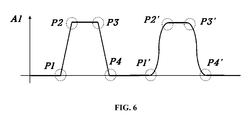
- FIG. 6 shows an example of position-dependent changes in the aluminum (Al) content of low refractive index layers and high refractive index layers of DBR unit layers of the light emitting diode shown in FIG. 5 in which a first transition portion and a second transition portion in the form of quadratic curves are formed in one of the DBR unit layers.
- the formation of the first and second transition portions can prevent a rapid change in energy band, leading to a reduction in the electrical resistance of the DBR unit layer.
- a metal electrode including silver (Ag) may be used as a reflective layer.
- silver has substantially low reflectance values in the UVA wavelength band of 315 nm to 420 nm despite its very high reflectance in the blue wavelength band, as shown in FIG. 1 . Accordingly, the use of silver as a material for a reflective layer is not suitable for the fabrication of a white light emitting diode using the UVA wavelength band.
- Aluminum (Al) may be used as a material for a reflective layer or electrode for reflecting light of a UVA wavelength band.
- Aluminum (Al) has high reflectance values in the UVA wavelength band, as shown in FIG. 1 , but has poor ohmic contact with a p-type semiconductor layer.
- the use of an aluminum electrode involves the use of a diffusion barrier layer, together with a process for forming the diffusion barrier layer.
- FIG. 2 is a longitudinal sectional view of a light emitting diode according to one embodiment of the present invention
- FIG. 3 shows wavelength-dependent changes in the reflectance of a light emitting diode according to one embodiment of the present invention
- FIG. 4 shows an example of position-dependent changes in the aluminum (Al) content of low refractive index layers and high refractive index layers of DBR unit layers constituting a second conductivity type reflective layer of a light emitting diode according to one embodiment of the present invention
- FIG. Al aluminum
- FIG. 5 shows a further example of position-dependent changes in the aluminum (Al) content of low refractive index layers and high refractive index layers of DBR unit layers constituting a second conductivity type reflective layer of a light emitting diode according to one embodiment of the present invention
- FIG. 6 shows various composition profiles of aluminum included in DBR unit layers.
- the light emitting diodes exemplified in these figures are flip-chip light emitting diodes. Although the following description is focused on flip-chip light emitting diodes, it should be noted that the same description is also applicable to vertical light emitting diodes. It should also be noted that the thickness of each layer in the drawings is exaggerated or schematically illustrated for convenience in description.
- FIG. 2 illustrates a light emitting diode according to one embodiment of the present invention.
- the light emitting diode includes a sapphire substrate 10 , a first conductivity type semiconductor layer 20 , an active layer 30 , a second conductivity type semiconductor layer 40 , a second conductivity type reflective layer 50 , a first electrode 80 , a reflective part as a second electrode, and a phase-matching layer 90 .
- Each of the first conductivity type semiconductor layer 20 and the second conductivity type semiconductor layer 40 has a front side and a back side. As illustrated, the first conductivity type semiconductor layer 20 is an n-type semiconductor layer and the second conductivity type semiconductor layer 40 is a p-type semiconductor layer. In this figure, the front and back sides of each of the first conductivity type semiconductor layer 20 , the active layer 30 , and the second conductivity type reflective layer 50 refer to the sides directed toward the top and bottom, respectively.
- the active layer 30 is formed between the back side of the first conductivity type semiconductor layer 20 and the front side of the second conductivity type semiconductor layer 40 .
- the active layer 30 is a layer where electrons recombine with holes to produce light.
- the active layer 30 may have a multiple quantum well (MQW) structure.
- the active layer 30 may be a semiconductor layer composed of a nitride, such as InGaN, AlGaN, AlGaInN or GaN.
- the first conductivity type semiconductor layer 20 , the active layer 30 , and the second conductivity type semiconductor layer 40 may be formed by suitable deposition and epitaxy processes, such as chemical vapor deposition (CVD), metal organic chemical vapor deposition (MOCVD), plasma-enhanced chemical vapor deposition (PECVD), molecular beam epitaxy (MBE), and hydride vapor phase epitaxy (HVPE).
- CVD chemical vapor deposition
- MOCVD metal organic chemical vapor deposition
- PECVD plasma-enhanced chemical vapor deposition
- MBE molecular beam epitaxy
- HVPE hydride vapor phase epitaxy
- the first electrode 80 is an element electrically connected to the first conductivity type semiconductor layer 20 .
- the reflective part is formed on the back side of the second conductivity type reflective layer and functions as a second electrode.
- the reflective part consists of a second conductivity type intermediate layer 72 for improving ohmic contact and a reflective metal layer 74 for reflecting light of UVA and blue wavelength bands.
- the first electrode 80 is an electrode electrically connected to the first conductivity type semiconductor layer 20 and the reflective part is electrically connected to the second conductivity type semiconductor layer 40 to function as a second electrode.
- the second conductivity type reflective layer 50 functions as a first reflective layer, which will be explained below
- the reflective metal layer 74 of the reflective part functions as a second reflective layer.
- the second conductivity type intermediate layer 72 may substantially have a thickness of 10 nm to 150 nm.
- the second conductivity type reflective layer 50 is formed on the back side of the second conductivity type semiconductor layer 40 , that is, between the back side of the second conductivity type semiconductor layer 40 and the reflective part, to reflect light of a short wavelength band entering through the second conductivity type semiconductor layer 40 from the active layer.
- the short wavelength is substantially from 315 nm to 420 nm.
- the second conductivity type reflective layer 50 includes DBR unit layers 50 a , 50 b , 50 c , . . . , 50 z .
- the DBR unit layer 50 a is explained as a representative example of the DBR unit layers but the same explanation of the DBR unit layer 50 a is made for the other DBR unit layers.
- the DBR unit layer 50 a includes a low refractive index layer 50 a 1 and a high refractive index layer 50 a 2 adjacent to each other.
- the low refractive index layer 50 a 1 and the high refractive index layer 50 a 2 include Al x Ga 1-x N (0 ⁇ x ⁇ 1) and Al y Ga 1-y N (0 ⁇ y ⁇ 1, y ⁇ x), respectively.
- the number of the DBR unit layers 50 a , 50 b , 50 c , . . . , 50 z in the second conductivity type reflective layer 50 is variable and may be adjusted such that the reflectance of the second conductivity type reflective layer 50 is substantially 80% or higher.
- the term “adjacent” used in the explanation of the positions of the low refractive index layer 50 a 1 and the high refractive index layer 50 a 2 means that the low refractive index layer 50 a 1 may directly neighbor the high refractive index layer 50 a 2 without an intervening element therebetween or an intervening element may be present between the low refractive index layer 50 a 1 and the high refractive index layer 50 a 2 .
- the low refractive index layers 50 a 1 and the high refractive index layers 50 a 2 are repeated alternately to form a continuous pattern in the DBR unit layers 50 a , 50 b , 50 c , . . . , 50 z of the second conductivity type reflective layer 50 .
- the second conductivity type reflective layer 50 is a p-type DBR.
- the low refractive index layer 50 a 1 and the high refractive index layer 50 a 2 include Al x Ga 1-x N (0 ⁇ x ⁇ 1) and Al y Ga 1-y N (0 ⁇ y ⁇ 1, y ⁇ x), respectively, as described above, and the Al content of the low refractive index layer 50 a 1 is always higher than that of the high refractive index layer 50 a 2 because the refractive index of GaN ( ⁇ 2.4 in the UV band) is lower than that of AlN.
- the low refractive index layer 50 a 1 and the high refractive index layer 50 a 2 may be, for example, composed of AlN and GaN, respectively.
- the doping concentration of the second conductivity type dopant in the DBR unit layer 50 z placed closest to the second electrode is higher than those in the other DBR unit layers. This concentration profile can improve the ohmic contact with the second electrode.
- the DBR unit layer 50 z placed closest to the p-type electrode may be a p-type semiconductor layer doped with the dopant at a high concentration up to a maximum of 5 ⁇ 10 20 cm ⁇ 3 .
- the first doping concentration may be lower than the second doping concentration.
- This doping concentration profile can reduce the occurrence of free-carrier absorption in the second conductivity type reflective layer 50 because free-carrier absorption occurs relatively frequently in the DBR unit layers placed relatively close to the active layer 30 compared to in the other DBR unit layers.
- the second doping concentration may be substantially from 1 ⁇ 10 18 cm ⁇ 3 to 1 ⁇ 10 21 cm ⁇ 3 and the first doping concentration may be substantially from 1 ⁇ 10 16 cm ⁇ 3 to 5 ⁇ 10 17 cm ⁇ 3 .
- the thickness of the second conductivity type reflective layer 50 may be substantially from 60 nm to 1500 nm and each DBR unit layer (for example, 50 a ) may be substantially from 60 nm to 100 nm.
- each of the low refractive index layer 50 a 1 and the high refractive index layer 50 a 2 may be substantially from 30 nm to 50 nm.
- the phase-matching layer 90 is added between the second conductivity type semiconductor layer 40 and the second conductivity type reflective layer 50 to maximize the effective reflectance of the reflective layers.
- the doping concentration of the second conductivity type dopant in the phase-matching layer 90 is also maintained at a lower level than the second doping concentration. This concentration profile can reduce the occurrence of free-carrier absorption.
- the second doping concentration may be substantially from 1 ⁇ 10 18 cm ⁇ 3 to 1 ⁇ 10 21 cm ⁇ 3 and the doping concentrations of the second conductivity type dopant both in the initial three DBR unit layers 50 a , 50 b , and 50 c and in the phase-matching layer may be substantially from 1 ⁇ 10 16 cm ⁇ 3 to 5 ⁇ 10 17 cm ⁇ 3 .
- the phase-matching layer 90 may include Al x Ga 1-x N (0 ⁇ x ⁇ 1) and may have a thickness of 5 nm to 50 nm
- the light emitting diode of the present invention is constructed to include the second conductivity type reflective layer 50 as a first reflective layer for reflecting light of a UVA wavelength band and the reflective metal layer 74 as a second reflective layer for reflecting light of a UVA wavelength band and light of a blue wavelength band. Due to this construction, the light emitting diode of the present invention has high reflectance in a broad wavelength region, including UVA and blue wavelength bands, achieving further improved light extraction efficiency. Furthermore, the conductivity type DBR reflects light propagating through the p-type semiconductor layer, achieving improved light efficiency. The formation of the conductivity type DBR can advantageously eliminate the need for additional processes for the formation of a non-conductivity type DBR and current paths.
- Section 1 is a wavelength band shorter than Section 2 (S2).
- Section 1 and shorter sections correspond to UVB and UVC wavelength bands that are not used in white light emitting diodes.
- Section 2 is a portion of the UVA wavelength band (315 nm to 420 nm) and is mostly reflected from the second conductivity type reflective layer 50 illustrated in FIG. 2 .
- the second conductivity type reflective layer 50 shows a reflectance of ⁇ 90% ( ⁇ 0.9), which is given by the red curve in Section 2.
- Section 3 corresponds to a portion of the UVA wavelength band and the blue wavelength band.
- the second conductivity type reflective layer 50 as a first reflective layer reflects light of a UVA wavelength band and the reflective metal layer 74 as a second reflective layer reflects light of a UVA wavelength band and light of a blue wavelength band such that the light emitting diode has high reflectance in a broad wavelength band, including UVA, achieving further improved light extraction efficiency.
- the low refractive index layer 50 a 1 and the high refractive index layer 50 a 2 of each of the DBR unit layers include Al x Ga 1-x N (0 ⁇ x ⁇ 1) and Al y Ga 1-y N (0 ⁇ y ⁇ 1, y ⁇ x), respectively.
- the aluminum (Al) content of the second conductivity type reflective layer 50 may vary and some examples thereof are graphically shown in FIGS. 4 to 6 . In each graph, the x-axis shows the position of the second conductivity type reflective layer 50 and the y-axis shows the Al content when the second conductivity type reflective layer 50 is positioned vertically.
- a represents the low refractive index layer 50 a 1
- b represents the high refractive index layer 50 a 2
- the sum a+b is the DBR unit 50 a .
- the low refractive index layer 50 a 1 is substantially an AlN layer where the Al content is highest and the high refractive index layer 50 a 2 is substantially a GaN layer where the Al content is lowest. Accordingly, the AlN and GaN layers are repeated in an alternating pattern in the second conductivity type reflective layer 50 .
- each of the DBR unit layers of the second conductivity type reflective layer 50 includes a first transition portion t 1 formed between the low refractive index layer 50 a 1 and the high refractive index layer 50 a 2 and whose Al content gradually decreases from the front to the back and a second transition portion t 2 formed between the high refractive index layer 50 a 2 and the low refractive index layer 50 a 1 of the next adjacent DBR unit layer ( 50 b of FIG. 2 ) and whose Al content gradually increases from the front to the back.
- t 1 formed between the low refractive index layer 50 a 1 and the high refractive index layer 50 a 2 and whose Al content gradually decreases from the front to the back
- a second transition portion t 2 formed between the high refractive index layer 50 a 2 and the low refractive index layer 50 a 1 of the next adjacent DBR unit layer ( 50 b of FIG. 2 ) and whose Al content gradually increases from the front to the back.
- the low refractive index layer is represented by 0.5t 2 +a+0.5t 1
- the high refractive index layer is represented by 0.5t 1 +b+0.5t 2
- the thickness of one DBR unit layer is represented by a+b+t 1 +t 2 .
- the DBR unit layer may be designed such that the optical thickness (i.e. a+b+t 1 +t 2 ) is ⁇ /2.
- Each of the low refractive index layer 50 a 1 and the high refractive index layer 50 a 2 of the DBR unit layer may be designed to have a thickness of ⁇ /4.
- the Al content profile of each of the first transition portion t 1 and the second transition portion t 2 may vary, for example, linearly or in the form of a quadratic curve.
- the starting point P 3 and the end point P 4 of the first transition portion t 1 and the starting point P 1 and the end point P 2 of the second transition portion t 2 are heterojunctions where the content of Al is changed rapidly rather than gradually. Only these points can be subjected to delta doping to prevent a rapid change in energy band.
- the Al content profiles have been explained herein with reference to the drawings, the Ga content also varies in response to the Al content because the DBR unit layers are composed of Al x Ga 1-x N (0 ⁇ x ⁇ 1) and Al y Ga 1-y N (0 ⁇ y ⁇ 1, y ⁇ x).
- delta doping is a technique to obtain a doping profile that looks like a delta function.
- high background doping leads to an overall increase in the occurrence of free-carrier absorption.
- the occurrence of free-carrier absorption can be prevented by adjusting the second doping concentration to the level of 1 ⁇ 10 18 cm ⁇ 3 to 1 ⁇ 10 21 cm ⁇ 3 and applying delta doping to only the portions, i.e. the transition portions t 1 and t 2 , where the content of Al varies.
- the adjustment of the second doping concentration and the delta doping can reduce a rapid change in energy band with varying Al content, leading to a reduction in the resistance of the second conductivity type reflective layer 50 .
- the new concept of light emitting diode of the present invention does not require the use of a reflective metal electrode, such as a silver or aluminum electrode that is not suitable for the formation of current paths due to its poor mechanical/electrical connection to a p-type semiconductor layer, unlike conventional light emitting diodes in which a non-conductivity type DBR is formed on a p-type semiconductor.
- the light efficiency of the light emitting diode according to the present invention can be considerably improved without the need to use an additional reflective metal layer.
Priority Applications (3)
| Application Number | Priority Date | Filing Date | Title |
|---|---|---|---|
| US15/693,159 US9985176B2 (en) | 2016-03-17 | 2017-08-31 | Light emitting diode with reflective part for UVA and blue wavelengths |
| US15/962,727 US10217899B2 (en) | 2016-03-17 | 2018-04-25 | Light emitting diode with reflective part for UVA and blue wavelengths |
| US16/245,405 US10622512B2 (en) | 2016-03-17 | 2019-01-11 | Light emitting diode with reflective part for UVA and blue wavelengths |
Applications Claiming Priority (2)
| Application Number | Priority Date | Filing Date | Title |
|---|---|---|---|
| KR10-2016-0032026 | 2016-03-17 | ||
| KR1020160032026A KR20170108321A (ko) | 2016-03-17 | 2016-03-17 | 발광 다이오드 |
Related Child Applications (1)
| Application Number | Title | Priority Date | Filing Date |
|---|---|---|---|
| US15/693,159 Continuation US9985176B2 (en) | 2016-03-17 | 2017-08-31 | Light emitting diode with reflective part for UVA and blue wavelengths |
Publications (2)
| Publication Number | Publication Date |
|---|---|
| US20170271555A1 US20170271555A1 (en) | 2017-09-21 |
| US9853187B2 true US9853187B2 (en) | 2017-12-26 |
Family
ID=57483232
Family Applications (4)
| Application Number | Title | Priority Date | Filing Date |
|---|---|---|---|
| US15/356,262 Active US9853187B2 (en) | 2016-03-17 | 2016-11-18 | Light emitting diode |
| US15/693,159 Active US9985176B2 (en) | 2016-03-17 | 2017-08-31 | Light emitting diode with reflective part for UVA and blue wavelengths |
| US15/962,727 Active US10217899B2 (en) | 2016-03-17 | 2018-04-25 | Light emitting diode with reflective part for UVA and blue wavelengths |
| US16/245,405 Active US10622512B2 (en) | 2016-03-17 | 2019-01-11 | Light emitting diode with reflective part for UVA and blue wavelengths |
Family Applications After (3)
| Application Number | Title | Priority Date | Filing Date |
|---|---|---|---|
| US15/693,159 Active US9985176B2 (en) | 2016-03-17 | 2017-08-31 | Light emitting diode with reflective part for UVA and blue wavelengths |
| US15/962,727 Active US10217899B2 (en) | 2016-03-17 | 2018-04-25 | Light emitting diode with reflective part for UVA and blue wavelengths |
| US16/245,405 Active US10622512B2 (en) | 2016-03-17 | 2019-01-11 | Light emitting diode with reflective part for UVA and blue wavelengths |
Country Status (3)
| Country | Link |
|---|---|
| US (4) | US9853187B2 (ja) |
| JP (3) | JP6039848B1 (ja) |
| KR (1) | KR20170108321A (ja) |
Cited By (12)
| Publication number | Priority date | Publication date | Assignee | Title |
|---|---|---|---|---|
| US10217899B2 (en) * | 2016-03-17 | 2019-02-26 | Lumens Co., Ltd. | Light emitting diode with reflective part for UVA and blue wavelengths |
| US20210351230A1 (en) | 2017-11-27 | 2021-11-11 | Seoul Viosys Co., Ltd. | Light emitting diode (led) stack for a display |
| US11282981B2 (en) | 2017-11-27 | 2022-03-22 | Seoul Viosys Co., Ltd. | Passivation covered light emitting unit stack |
| US11289536B2 (en) | 2017-11-27 | 2022-03-29 | Seoul Viosys Co., Ltd. | Light emitting device having commonly connected LED sub-units |
| US11289461B2 (en) | 2017-12-05 | 2022-03-29 | Seoul Viosys Co., Ltd. | Light emitting device with LED stack for display and display apparatus having the same |
| US11522008B2 (en) | 2018-01-02 | 2022-12-06 | Seoul Viosys Co., Ltd. | Display device having light emitting stacked structure |
| US11522006B2 (en) | 2017-12-21 | 2022-12-06 | Seoul Viosys Co., Ltd. | Light emitting stacked structure and display device having the same |
| US11527513B2 (en) | 2017-12-20 | 2022-12-13 | Seoul Viosys Co., Ltd. | LED unit for display and display apparatus having the same |
| US11527519B2 (en) | 2017-11-27 | 2022-12-13 | Seoul Viosys Co., Ltd. | LED unit for display and display apparatus having the same |
| US11552061B2 (en) | 2017-12-22 | 2023-01-10 | Seoul Viosys Co., Ltd. | Light emitting device with LED stack for display and display apparatus having the same |
| US11557577B2 (en) | 2018-01-03 | 2023-01-17 | Seoul Viosys Co., Ltd. | Light emitting device with LED stack for display and display apparatus having the same |
| US11804512B2 (en) | 2017-12-14 | 2023-10-31 | Seoul Viosys Co., Ltd. | Light emitting stacked structure and display device having the same |
Families Citing this family (6)
| Publication number | Priority date | Publication date | Assignee | Title |
|---|---|---|---|---|
| US11201261B2 (en) | 2017-02-17 | 2021-12-14 | Dowa Electronics Materials Co., Ltd. | Deep ultraviolet light emitting element and method of manufacturing the same |
| JP6727185B2 (ja) * | 2017-12-28 | 2020-07-22 | 日機装株式会社 | 窒化物半導体発光素子 |
| KR20190104902A (ko) | 2018-03-02 | 2019-09-11 | 마이크로머티어리얼즈 엘엘씨 | 금속 산화물들을 제거하기 위한 방법들 |
| KR101933120B1 (ko) * | 2018-09-21 | 2018-12-27 | 박민재 | 밀링 가공 장치 |
| KR101933121B1 (ko) * | 2018-09-21 | 2018-12-27 | 박민재 | 밀링 가공 장치 제작방법 |
| CN110299472B (zh) * | 2019-06-28 | 2022-09-09 | 京东方科技集团股份有限公司 | 一种阵列基板、显示面板及显示装置 |
Citations (14)
| Publication number | Priority date | Publication date | Assignee | Title |
|---|---|---|---|---|
| JP2001060717A (ja) | 1999-08-23 | 2001-03-06 | Nippon Sheet Glass Co Ltd | 発光サイリスタおよび自己走査型発光装置 |
| JP2006100420A (ja) | 2004-09-28 | 2006-04-13 | Toyoda Gosei Co Ltd | Iii族窒化物系化合物半導体発光素子 |
| US20080128745A1 (en) * | 2006-12-04 | 2008-06-05 | Mastro Michael A | Group iii-nitride growth on silicon or silicon germanium substrates and method and devices therefor |
| US7498182B1 (en) * | 2005-03-18 | 2009-03-03 | The United States Of America As Represented By The Secretary Of The Army | Method of manufacturing an ultraviolet light emitting AlGaN composition and ultraviolet light emitting device containing same |
| WO2009069929A2 (en) | 2007-11-26 | 2009-06-04 | Lg Innotek Co., Ltd | Semiconductor light emitting device |
| US20100200881A1 (en) * | 2007-06-28 | 2010-08-12 | Kyocera Corporation | Light Emitting Element and Illumination Device |
| JP2011216882A (ja) | 2010-03-31 | 2011-10-27 | Seoul Opto Devices Co Ltd | 高効率発光ダイオード及びその製造方法 |
| US20110309326A1 (en) * | 2010-06-18 | 2011-12-22 | Remigijus Gaska | Deep ultraviolet light emitting diode |
| US20130146907A1 (en) * | 2011-12-12 | 2013-06-13 | Sensor Electronic Technology, Inc. | Ultraviolet Reflective Contact |
| US20130193409A1 (en) * | 2010-06-18 | 2013-08-01 | Sensor Electronic Technology, Inc. | Deep Ultraviolet Light Emitting Diode |
| KR20140016512A (ko) | 2012-07-30 | 2014-02-10 | 주식회사 세미콘라이트 | 반도체 발광소자 |
| JP2014103240A (ja) | 2012-11-20 | 2014-06-05 | Stanley Electric Co Ltd | 半導体発光素子 |
| KR20150136264A (ko) | 2014-05-27 | 2015-12-07 | 서울바이오시스 주식회사 | 발광 소자 |
| US20160072015A1 (en) * | 2014-09-04 | 2016-03-10 | Seoul Viosys Co., Ltd. | Vertical ultraviolet light emitting device and method for manufacturing the same |
Family Cites Families (14)
| Publication number | Priority date | Publication date | Assignee | Title |
|---|---|---|---|---|
| JP2904227B2 (ja) * | 1991-03-08 | 1999-06-14 | 日本電信電話株式会社 | 面発光レーザ |
| US5838707A (en) * | 1996-12-27 | 1998-11-17 | Motorola, Inc. | Ultraviolet/visible light emitting vertical cavity surface emitting laser and method of fabrication |
| JP2002026385A (ja) * | 2000-07-06 | 2002-01-25 | Hitachi Cable Ltd | 発光ダイオード |
| JP3763737B2 (ja) * | 2000-11-28 | 2006-04-05 | 株式会社東芝 | 半導体発光素子 |
| US20070285000A1 (en) * | 2004-09-10 | 2007-12-13 | Luminus Devices, Inc. | Polarization recycling illumination assembly and methods |
| TWI267212B (en) * | 2004-12-30 | 2006-11-21 | Ind Tech Res Inst | Quantum dots/quantum well light emitting diode |
| US20090001389A1 (en) * | 2007-06-28 | 2009-01-01 | Motorola, Inc. | Hybrid vertical cavity of multiple wavelength leds |
| JP5378131B2 (ja) * | 2009-09-25 | 2013-12-25 | シャープ株式会社 | 窒化物半導体発光ダイオード素子 |
| US10134948B2 (en) * | 2011-02-25 | 2018-11-20 | Sensor Electronic Technology, Inc. | Light emitting diode with polarization control |
| KR101981119B1 (ko) * | 2011-11-25 | 2019-05-22 | 엘지이노텍 주식회사 | 자외선 반도체 발광 소자 |
| US8907319B2 (en) * | 2011-12-12 | 2014-12-09 | Lg Innotek Co., Ltd. | Light emitting device package |
| US9312432B2 (en) * | 2012-03-13 | 2016-04-12 | Tsmc Solid State Lighting Ltd. | Growing an improved P-GaN layer of an LED through pressure ramping |
| TW201340405A (zh) * | 2012-03-30 | 2013-10-01 | Lextar Electronics Corp | 發光二極體 |
| KR20170108321A (ko) * | 2016-03-17 | 2017-09-27 | 주식회사 루멘스 | 발광 다이오드 |
-
2016
- 2016-03-17 KR KR1020160032026A patent/KR20170108321A/ko not_active Application Discontinuation
- 2016-05-13 JP JP2016097186A patent/JP6039848B1/ja active Active
- 2016-11-04 JP JP2016216305A patent/JP6320486B2/ja not_active Expired - Fee Related
- 2016-11-18 US US15/356,262 patent/US9853187B2/en active Active
-
2017
- 2017-08-31 US US15/693,159 patent/US9985176B2/en active Active
-
2018
- 2018-04-03 JP JP2018071697A patent/JP6722221B2/ja not_active Expired - Fee Related
- 2018-04-25 US US15/962,727 patent/US10217899B2/en active Active
-
2019
- 2019-01-11 US US16/245,405 patent/US10622512B2/en active Active
Patent Citations (15)
| Publication number | Priority date | Publication date | Assignee | Title |
|---|---|---|---|---|
| JP2001060717A (ja) | 1999-08-23 | 2001-03-06 | Nippon Sheet Glass Co Ltd | 発光サイリスタおよび自己走査型発光装置 |
| JP2006100420A (ja) | 2004-09-28 | 2006-04-13 | Toyoda Gosei Co Ltd | Iii族窒化物系化合物半導体発光素子 |
| US7498182B1 (en) * | 2005-03-18 | 2009-03-03 | The United States Of America As Represented By The Secretary Of The Army | Method of manufacturing an ultraviolet light emitting AlGaN composition and ultraviolet light emitting device containing same |
| US20080128745A1 (en) * | 2006-12-04 | 2008-06-05 | Mastro Michael A | Group iii-nitride growth on silicon or silicon germanium substrates and method and devices therefor |
| US20100200881A1 (en) * | 2007-06-28 | 2010-08-12 | Kyocera Corporation | Light Emitting Element and Illumination Device |
| JP2011504660A (ja) | 2007-11-26 | 2011-02-10 | エルジー イノテック カンパニー リミテッド | 半導体発光素子 |
| WO2009069929A2 (en) | 2007-11-26 | 2009-06-04 | Lg Innotek Co., Ltd | Semiconductor light emitting device |
| JP2011216882A (ja) | 2010-03-31 | 2011-10-27 | Seoul Opto Devices Co Ltd | 高効率発光ダイオード及びその製造方法 |
| US20110309326A1 (en) * | 2010-06-18 | 2011-12-22 | Remigijus Gaska | Deep ultraviolet light emitting diode |
| US20130193409A1 (en) * | 2010-06-18 | 2013-08-01 | Sensor Electronic Technology, Inc. | Deep Ultraviolet Light Emitting Diode |
| US20130146907A1 (en) * | 2011-12-12 | 2013-06-13 | Sensor Electronic Technology, Inc. | Ultraviolet Reflective Contact |
| KR20140016512A (ko) | 2012-07-30 | 2014-02-10 | 주식회사 세미콘라이트 | 반도체 발광소자 |
| JP2014103240A (ja) | 2012-11-20 | 2014-06-05 | Stanley Electric Co Ltd | 半導体発光素子 |
| KR20150136264A (ko) | 2014-05-27 | 2015-12-07 | 서울바이오시스 주식회사 | 발광 소자 |
| US20160072015A1 (en) * | 2014-09-04 | 2016-03-10 | Seoul Viosys Co., Ltd. | Vertical ultraviolet light emitting device and method for manufacturing the same |
Non-Patent Citations (2)
| Title |
|---|
| Notice of Allowance dated Oct. 18, 2016 in a corresponding Japanese Patent Application No. JP2016-097186 with English language translation. |
| Office Action dated Aug. 2, 2016 in a corresponding Japanese Patent Application No. JP2016-097186. |
Cited By (24)
| Publication number | Priority date | Publication date | Assignee | Title |
|---|---|---|---|---|
| US20190148585A1 (en) * | 2016-03-17 | 2019-05-16 | Lumens Co., Ltd. | Light emitting diode with reflective part for uva and blue wavelengths |
| US10622512B2 (en) * | 2016-03-17 | 2020-04-14 | Lumens Co., Ltd. | Light emitting diode with reflective part for UVA and blue wavelengths |
| US10217899B2 (en) * | 2016-03-17 | 2019-02-26 | Lumens Co., Ltd. | Light emitting diode with reflective part for UVA and blue wavelengths |
| US11527519B2 (en) | 2017-11-27 | 2022-12-13 | Seoul Viosys Co., Ltd. | LED unit for display and display apparatus having the same |
| US20210351230A1 (en) | 2017-11-27 | 2021-11-11 | Seoul Viosys Co., Ltd. | Light emitting diode (led) stack for a display |
| US11282981B2 (en) | 2017-11-27 | 2022-03-22 | Seoul Viosys Co., Ltd. | Passivation covered light emitting unit stack |
| US11289536B2 (en) | 2017-11-27 | 2022-03-29 | Seoul Viosys Co., Ltd. | Light emitting device having commonly connected LED sub-units |
| US11935912B2 (en) | 2017-11-27 | 2024-03-19 | Seoul Viosys Co., Ltd. | Light emitting device having commonly connected LED sub-units |
| US11610939B2 (en) | 2017-11-27 | 2023-03-21 | Seoul Viosys Co., Ltd. | Light emitting diode (LED) stack for a display |
| US11563052B2 (en) | 2017-11-27 | 2023-01-24 | Seoul Viosys Co., Ltd. | Light emitting diode (LED) stack for a display |
| US11532664B2 (en) * | 2017-11-27 | 2022-12-20 | Seoul Viosys Co., Ltd. | Light emitting diode (LED) stack for a display |
| US11289461B2 (en) | 2017-12-05 | 2022-03-29 | Seoul Viosys Co., Ltd. | Light emitting device with LED stack for display and display apparatus having the same |
| US11804511B2 (en) | 2017-12-05 | 2023-10-31 | Seoul Viosys Co., Ltd. | Light emitting device with LED stack for display and display apparatus having the same |
| US11804512B2 (en) | 2017-12-14 | 2023-10-31 | Seoul Viosys Co., Ltd. | Light emitting stacked structure and display device having the same |
| US11527514B2 (en) | 2017-12-20 | 2022-12-13 | Seoul Viosys Co., Ltd. | LED unit for display and display apparatus having the same |
| US11552057B2 (en) | 2017-12-20 | 2023-01-10 | Seoul Viosys Co., Ltd. | LED unit for display and display apparatus having the same |
| US11527513B2 (en) | 2017-12-20 | 2022-12-13 | Seoul Viosys Co., Ltd. | LED unit for display and display apparatus having the same |
| US11522006B2 (en) | 2017-12-21 | 2022-12-06 | Seoul Viosys Co., Ltd. | Light emitting stacked structure and display device having the same |
| US11756984B2 (en) | 2017-12-21 | 2023-09-12 | Seoul Viosys Co., Ltd. | Light emitting stacked structure and display device having the same |
| US11973104B2 (en) | 2017-12-21 | 2024-04-30 | Seoul Viosys Co., Ltd. | Light emitting stacked structure and display device having the same |
| US11552061B2 (en) | 2017-12-22 | 2023-01-10 | Seoul Viosys Co., Ltd. | Light emitting device with LED stack for display and display apparatus having the same |
| US11522008B2 (en) | 2018-01-02 | 2022-12-06 | Seoul Viosys Co., Ltd. | Display device having light emitting stacked structure |
| US11557577B2 (en) | 2018-01-03 | 2023-01-17 | Seoul Viosys Co., Ltd. | Light emitting device with LED stack for display and display apparatus having the same |
| US11923348B2 (en) | 2018-01-03 | 2024-03-05 | Seoul Viosys Co., Ltd. | Light emitting device with LED stack for display and display apparatus having the same |
Also Published As
| Publication number | Publication date |
|---|---|
| US20180069152A1 (en) | 2018-03-08 |
| JP2017168797A (ja) | 2017-09-21 |
| US10217899B2 (en) | 2019-02-26 |
| US20180240938A1 (en) | 2018-08-23 |
| JP6320486B2 (ja) | 2018-05-09 |
| JP2018113477A (ja) | 2018-07-19 |
| JP2017168811A (ja) | 2017-09-21 |
| JP6039848B1 (ja) | 2016-12-07 |
| US20190148585A1 (en) | 2019-05-16 |
| KR20170108321A (ko) | 2017-09-27 |
| US20170271555A1 (en) | 2017-09-21 |
| US10622512B2 (en) | 2020-04-14 |
| US9985176B2 (en) | 2018-05-29 |
| JP6722221B2 (ja) | 2020-07-15 |
Similar Documents
| Publication | Publication Date | Title |
|---|---|---|
| US10622512B2 (en) | Light emitting diode with reflective part for UVA and blue wavelengths | |
| US7906791B2 (en) | Semiconductor light emitting element | |
| KR101100681B1 (ko) | 반도체 발광소자 | |
| US20090127572A1 (en) | Nitride Semiconductor Light Emitting Device | |
| JP3839799B2 (ja) | 半導体発光素子 | |
| US9853182B2 (en) | Gallium nitride-based light emitting diode | |
| KR20080087135A (ko) | 질화물 반도체 발광 소자 | |
| KR20140078977A (ko) | 고효율 발광 다이오드 | |
| KR20090058364A (ko) | 질화갈륨계 반도체 발광소자 | |
| US10868213B2 (en) | LED utilizing internal color conversion with light extraction enhancements | |
| WO2020005827A1 (en) | Led utilizing internal color conversion with light extraction enhancements | |
| KR101423720B1 (ko) | 다중양자웰 구조의 활성 영역을 갖는 발광 소자 및 그제조방법 | |
| KR102111140B1 (ko) | 발광 다이오드 및 그것을 제조하는 방법 | |
| KR101747349B1 (ko) | 반도체 발광소자 | |
| KR101138976B1 (ko) | 발광다이오드 | |
| JP2006040998A (ja) | 半導体発光素子、半導体発光素子用エピタキシャルウェハ | |
| EP2009707B1 (en) | Light emitting diode and method for manufacturing the same | |
| KR101117484B1 (ko) | 반도체 발광소자 | |
| KR101494331B1 (ko) | 플립 칩 구조의 질화물 반도체 발광소자 | |
| US20230070171A1 (en) | Light emitting diode and method of fabricating the same | |
| KR101115537B1 (ko) | 고효율 반도체 발광소자 | |
| KR20170108327A (ko) | 발광 다이오드 | |
| KR20160035250A (ko) | 발광 소자 | |
| KR101550951B1 (ko) | 발광소자 |
Legal Events
| Date | Code | Title | Description |
|---|---|---|---|
| AS | Assignment |
Owner name: LUMENS CO., LTD., KOREA, REPUBLIC OF Free format text: ASSIGNMENT OF ASSIGNORS INTEREST;ASSIGNOR:KIM, DAE WON;REEL/FRAME:040372/0696 Effective date: 20161117 |
|
| STCF | Information on status: patent grant |
Free format text: PATENTED CASE |
|
| MAFP | Maintenance fee payment |
Free format text: PAYMENT OF MAINTENANCE FEE, 4TH YR, SMALL ENTITY (ORIGINAL EVENT CODE: M2551); ENTITY STATUS OF PATENT OWNER: SMALL ENTITY Year of fee payment: 4 |