US9787012B2 - Terminal fitting with resilient pieces having thin plating region and thick plating region - Google Patents
Terminal fitting with resilient pieces having thin plating region and thick plating region Download PDFInfo
- Publication number
- US9787012B2 US9787012B2 US14/910,726 US201414910726A US9787012B2 US 9787012 B2 US9787012 B2 US 9787012B2 US 201414910726 A US201414910726 A US 201414910726A US 9787012 B2 US9787012 B2 US 9787012B2
- Authority
- US
- United States
- Prior art keywords
- terminal fitting
- connecting portion
- guiding
- plating film
- resilient pieces
- Prior art date
- Legal status (The legal status is an assumption and is not a legal conclusion. Google has not performed a legal analysis and makes no representation as to the accuracy of the status listed.)
- Active
Links
- 238000007747 plating Methods 0.000 title claims abstract description 61
- 230000013011 mating Effects 0.000 claims abstract description 10
- 238000002788 crimping Methods 0.000 claims description 29
- 239000010408 film Substances 0.000 description 61
- 239000010409 thin film Substances 0.000 description 9
- 230000000873 masking effect Effects 0.000 description 5
- 238000000034 method Methods 0.000 description 5
- 239000011347 resin Substances 0.000 description 5
- 229920005989 resin Polymers 0.000 description 5
- 230000002093 peripheral effect Effects 0.000 description 4
- 239000000243 solution Substances 0.000 description 4
- 230000015572 biosynthetic process Effects 0.000 description 3
- BQCADISMDOOEFD-UHFFFAOYSA-N Silver Chemical compound [Ag] BQCADISMDOOEFD-UHFFFAOYSA-N 0.000 description 2
- 230000008878 coupling Effects 0.000 description 2
- 238000010168 coupling process Methods 0.000 description 2
- 238000005859 coupling reaction Methods 0.000 description 2
- 238000002347 injection Methods 0.000 description 2
- 239000007924 injection Substances 0.000 description 2
- 229910052709 silver Inorganic materials 0.000 description 2
- 239000004332 silver Substances 0.000 description 2
- 238000005452 bending Methods 0.000 description 1
- 238000006243 chemical reaction Methods 0.000 description 1
- 239000011248 coating agent Substances 0.000 description 1
- 238000000576 coating method Methods 0.000 description 1
- 238000007598 dipping method Methods 0.000 description 1
- PCHJSUWPFVWCPO-UHFFFAOYSA-N gold Chemical compound [Au] PCHJSUWPFVWCPO-UHFFFAOYSA-N 0.000 description 1
- 239000010931 gold Substances 0.000 description 1
- 229910052737 gold Inorganic materials 0.000 description 1
- 238000003780 insertion Methods 0.000 description 1
- 230000037431 insertion Effects 0.000 description 1
- 239000000463 material Substances 0.000 description 1
- 229910052751 metal Inorganic materials 0.000 description 1
- 239000002184 metal Substances 0.000 description 1
- 239000007787 solid Substances 0.000 description 1
- 239000002699 waste material Substances 0.000 description 1
Images


Classifications
-
- H—ELECTRICITY
- H01—ELECTRIC ELEMENTS
- H01R—ELECTRICALLY-CONDUCTIVE CONNECTIONS; STRUCTURAL ASSOCIATIONS OF A PLURALITY OF MUTUALLY-INSULATED ELECTRICAL CONNECTING ELEMENTS; COUPLING DEVICES; CURRENT COLLECTORS
- H01R13/00—Details of coupling devices of the kinds covered by groups H01R12/70 or H01R24/00 - H01R33/00
- H01R13/02—Contact members
- H01R13/10—Sockets for co-operation with pins or blades
- H01R13/11—Resilient sockets
- H01R13/111—Resilient sockets co-operating with pins having a circular transverse section
-
- H—ELECTRICITY
- H01—ELECTRIC ELEMENTS
- H01R—ELECTRICALLY-CONDUCTIVE CONNECTIONS; STRUCTURAL ASSOCIATIONS OF A PLURALITY OF MUTUALLY-INSULATED ELECTRICAL CONNECTING ELEMENTS; COUPLING DEVICES; CURRENT COLLECTORS
- H01R13/00—Details of coupling devices of the kinds covered by groups H01R12/70 or H01R24/00 - H01R33/00
- H01R13/02—Contact members
- H01R13/03—Contact members characterised by the material, e.g. plating, or coating materials
-
- H—ELECTRICITY
- H01—ELECTRIC ELEMENTS
- H01R—ELECTRICALLY-CONDUCTIVE CONNECTIONS; STRUCTURAL ASSOCIATIONS OF A PLURALITY OF MUTUALLY-INSULATED ELECTRICAL CONNECTING ELEMENTS; COUPLING DEVICES; CURRENT COLLECTORS
- H01R4/00—Electrically-conductive connections between two or more conductive members in direct contact, i.e. touching one another; Means for effecting or maintaining such contact; Electrically-conductive connections having two or more spaced connecting locations for conductors and using contact members penetrating insulation
- H01R4/10—Electrically-conductive connections between two or more conductive members in direct contact, i.e. touching one another; Means for effecting or maintaining such contact; Electrically-conductive connections having two or more spaced connecting locations for conductors and using contact members penetrating insulation effected solely by twisting, wrapping, bending, crimping, or other permanent deformation
- H01R4/18—Electrically-conductive connections between two or more conductive members in direct contact, i.e. touching one another; Means for effecting or maintaining such contact; Electrically-conductive connections having two or more spaced connecting locations for conductors and using contact members penetrating insulation effected solely by twisting, wrapping, bending, crimping, or other permanent deformation by crimping
- H01R4/183—Electrically-conductive connections between two or more conductive members in direct contact, i.e. touching one another; Means for effecting or maintaining such contact; Electrically-conductive connections having two or more spaced connecting locations for conductors and using contact members penetrating insulation effected solely by twisting, wrapping, bending, crimping, or other permanent deformation by crimping for cylindrical elongated bodies, e.g. cables having circular cross-section
Definitions
- the present invention relates to a terminal fitting.
- a terminal fitting disclosed in Japanese Examined Patent Publication No. H02-38675 includes a connecting portion (electrical contact portion) in the form of a rectangular tube into which a mating male terminal is insertable.
- This connecting portion is immersed in a plating solution in a plating bath and the plating solution is injected from an injection nozzle to flow through the connecting portion with a tip opening of the connecting portion faced toward the injection nozzle in the plating bath, whereby a plating film is formed on the inner surface of the connecting portion.
- the connecting portion includes contact portions to be connected electrically to the male terminal on a pair of wall sides facing each other. According to the above configuration, it is possible to form thicker plating films on necessary parts including the contact portions than on other parts.
- the contact portions of the above-described conventional terminal fitting are provided only on parts of the inner surface of the connecting portion in a circumferential direction (pair of wall sides facing each other).
- the plating film is formed on the inner surface of the connecting portion over the entire circumference and the thick plating layer formed on parts other than the necessary parts such as the contact portions is useless.
- thick plating films can be formed only on the necessary parts by masking parts the inner surface of the connecting portion in the circumferential direction.
- the parts of the inner surface of the connecting portion in the circumferential direction are masked, there have been problems of difficult plating and lacking reality.
- the present invention was completed based on the above situation and aims to provide a terminal fitting in which thick plating films can be formed on necessary parts without requiring particularly complicated plating.
- the present invention is directed to a terminal fitting including a tubular connecting portion into which a mating male terminal is insertable.
- the connecting portion includes a plurality of resilient pieces circumferentially divided via expanding slots extending from a tip. Thick film portions with a thicker plating film than other parts are provided on inner surfaces of the plurality of resilient pieces. Contact areas capable of contacting the male terminal are provided on the thick film portions.
- the thick film portions and the contact areas are arranged continuously in a circumferential direction except at the positions of the expanding slots on an inner surface of the connecting portion near a tip. Accordingly, the plating films of the thick film portions can be formed easily without masking parts of the inner surface of the connecting portion in the circumferential direction. In addition, the contact areas can be formed on the thick film portions without waste.
- a terminal fitting is provided in which thick plating films can be formed on necessary parts without requiring particularly complicated plating.
- the terminal fitting may include a tubular crimping portion open toward a side opposite to a side where the connecting portion is open.
- a wire is connectable to an inner surface of the crimping portion by crimping.
- a thin film portion is provided on the inner surface of the crimping portion and has a thinner plating film than the thick film portions.
- a thick plating film of the crimping portion may cause cracks to be formed on the surface of the plating film of the crimping portion in a crimping process.
- the crimping portion is formed with the thin film portion. Therefore, cracks are unlikely to be formed on the surface of the plating film of the crimping portion. Further, cost is reduced since it is not necessary to form a thick plating film on the crimping portion.
- the contact area may include a guiding portion widened toward the tip and capable of guiding the male terminal into the connecting portion.
- a contact portion may be arranged behind the guiding portion in a guiding direction and may be configured for being connected to the male terminal when the male terminal is inserted properly.
- the thick film portion may be arranged across the contact portion and the guiding portion. Thus, the thick film portion is provided on both the guiding portion and the contact portion. Therefore, the connecting portion is protected by the thick film portions from an initial stage of guiding the male terminal into the connecting portion.
- the resilient piece may include a corner round portion in the form of a curved surface continuous from the inner surface of the resilient piece to a side surface facing the expanding slot. Additionally, the thick film portion may include a surface part in the form of a curved surface extending along the corner round portion. These shapes can prevent the edge-like contact areas from contacting the male terminal at the positions corresponding to the corner round portions of the resilient pieces and ensure the contact reliability of the male terminal with the contact areas.
- FIG. 1 is a perspective view of a terminal fitting of a first embodiment.
- FIG. 2 is a side view of the terminal fitting.
- FIG. 3 is a side view of the terminal fitting connected to a wire.
- FIG. 4 is a section of the terminal fitting.
- FIG. 5 is a section along A-A of FIG. 4 .
- FIG. 6 is a side view showing a state where the terminal fitting connected to the wire is in contact with a male terminal.
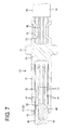
- FIG. 7 is a section showing the state where the terminal fitting connected to the wire is in contact with the male terminal.
- FIG. 8 is an enlarged section of an essential part of a terminal fitting of a second embodiment.
- a first embodiment of the present invention is described with reference to FIGS. 1 to 7 .
- a terminal fitting 10 of the first embodiment is formed into a shape long and narrow in a front-back direction as a whole such as by bending an electrically conductive metal plate and, as shown in FIG. 6 , includes a tubular connecting portion 11 into which a mating male terminal 60 is insertable from front and a crimping portion 12 arranged behind the connecting portion 11 .
- the male terminal 60 includes a connecting pin 61 in the form of a bar long and narrow in the front-back direction, specifically in the form of a cylindrical column.
- a resin member 62 for preventing electrification is incorporated on a tip side of the connecting pin 61 .
- the outer periphery of the resin member 62 is tapered to be narrower toward the tip side.
- the crimping portion 12 is in the form of a closed barrel and has a hollow cylindrical shape open backward. As shown in FIG. 7 , the crimping portion 12 is crimped and connected to a core portion 92 exposed by removing a coating 91 at a front end part of a wire 90 . An intermediate part of the crimping portion 12 in the front-back direction is deformed and narrowed over the entire circumference by being crimped.
- the connecting portion 11 is in the form of a cylindrical tube open forward and longer than the crimping portion 12 .
- the connecting portion 11 is formed with a plurality of expanding slots 13 at equal intervals in a circumferential direction. Each expanding slot 13 radially penetrates through the connecting portion 11 as shown in FIG. 5 and extends in the front-back direction to be open on the front end of the connecting portion 11 as shown in FIG. 1 .
- a plurality of resilient pieces 14 are separately provided between the expanding slots 13 on the connecting portion 11 .
- the inner surface of the resilient piece 14 in a natural state has a narrow portion 15 slightly radially narrowed and extending forward from the rear end and a guiding portion 16 widened toward the front end from a narrow end 19 of the narrow portion 15 on a front end part.
- a contact area 17 capable of electrically contacting the male terminal 60 is provided on the inner surface of the resilient piece 14 .
- the contact areas 17 are arranged continuously in a strip-like manner substantially over the entire circumference except at the positions of the respective expanding slots 13 on the inner surface of the connecting portion 11 near the front end.
- the contact area 17 is arranged in a predetermined area of the inner surface of the resilient piece 14 in the front-back direction across the narrow end 19 . As shown in FIG.
- the contact area 17 is provided with a contact portion 18 , which resiliently contacts the outer peripheral surface of the connecting pin 61 to establish an electrical connection when the connecting pin 61 of the male terminal 60 is inserted to a proper depth into the connecting portion 11 , behind the narrow end 19 .
- the terminal fitting 10 includes a solid coupling portion 20 having a circular cross-section between the connecting portion 11 and the crimping portion 12 .
- a circular flange portion 21 is provided to protrude in the circumferential direction on the outer peripheral surface of the coupling portion 20 .
- the plating film is composed of thick film portions 22 having a relatively large thickness and provided on parts of the inner surface of the connecting portion 11 corresponding to the aforementioned contact areas 17 and thin film portions 23 (not specifically shown) having a relatively small thickness and provided on parts excluding the contact areas 17 .
- surfaces (inner surfaces) of the thick film portions 22 serve as the contact areas 17 as shown in FIG.
- the thick film portions 22 are arranged continuously in a strip-like manner substantially over the entire circumference except at the positions of the respective expanding slots 13 on the inner surface of the connecting portion 11 near the front end and in predetermined areas of the inner surfaces of the respective resilient pieces 14 in the front-back direction across the narrow ends 19 as shown in FIGS. 1 and 4 .
- the thin film portions 23 are provided on all parts excluding the contact areas 17 , including the inner surface of the crimping portion 12 to be crimped to the core portion 92 of the wire 90 .
- predetermined plating is performed such as by immersing the entire terminal fitting 10 into a plating solution in an unillustrated plating bath. In this way, parts corresponding to the thin film portions 23 with a thin plating film are formed on the entire surface of the terminal fitting 10 . Subsequently, a tip part of the connecting portion 11 is likewise immersed into a plating solution in a likewise unillustrated plating bath with predetermined areas of the outer and inner surfaces of the connecting portion 11 masked. In this way, the thick film portions 22 with a thick plating film are formed to be laminated on the thin film portions 23 on the inner side of the connecting portion 11 .
- the resin member 62 is inserted into the connecting portion 11 without contacting the respective resilient pieces 14 , and a shoulder portion 66 of the tip part of the connecting pin 61 in the form of a curved surface on an outer peripheral side of a seating surface for receiving the resin member 62 first comes into contact with (first touches) the guiding portions 16 of the thick film portions 22 .
- each resilient piece 14 is resiliently deformed with the rear end thereof as a supporting point as coming into contact with the connecting pin 61 , and the narrow portion 15 becomes substantially horizontal in the front-back direction.
- the connecting pin 61 contacts the contact portion 18 of each thick film portion 22 of the connecting portion 11 with a resilient reaction force of each resilient piece 14 maintained, with the result that the terminal fitting 10 is held in a state conductively connected to the male terminal 60 .
- the connecting pin 61 is in contact with the contact portions 18 of the contact areas 17 substantially over the entire circumference except at the positions of the respective expanding slots 13 .
- the terminal fitting 10 and the male terminal 60 are respectively mounted in unillustrated connector housings and the aforementioned connecting operation is performed in conjunction with a connecting operation of the respective connector housings.
- the thick film portions 22 are arranged continuously in the circumferential direction except at the positions of the expanding slots 13 at the position of the connecting portion 11 near the front end according to the first embodiment, it is not necessary to partially mask the inner surface of the connecting portion 11 in the circumferential direction and special plating for masking in the circumferential direction is not necessary.
- the contact areas 17 are provided on the surfaces of the thick film portions 22 over the entire circumference, i.e. since the thick film portions 22 are substantially provided only on necessary parts without being wasted, cost is reduced.
- the thin film portions 23 can be provided on the parts where the plating film is not particularly necessary by providing the thick film portions 22 only on the substantially necessary parts, cost is more reduced. Particularly, if the plating film of the crimping portion 12 is thick, there is a possibility of causing cracks on the surface of the plating film of the crimping portion 12 in a crimping process. However, since the crimping portion 12 is provided with the thin film portion 23 according to the first embodiment, the formation of cracks on the surface of the plating film of the crimping portion 12 is prevented.
- the thick film portions 22 are provided also on the guiding portions 16 of the contact areas 17 , the connecting portion 11 is effectively protected by the thick film portions 22 from an initial stage of guiding the male terminal 60 into the connecting portion 11 and the exposure of a base material can be avoided.
- FIG. 8 shows an enlarged section of each resilient piece 14 provided with a thick film portion 22 in a terminal fitting 10 of a second embodiment of the present invention.
- a film formation mode of the thick film portion 22 on each resilient piece 14 is different from the first embodiment and the shape of a part of each resilient piece 14 covered with the thick film portion 22 is different from the first embodiment. Since the other points are the same as in the first embodiment, parts identical or similar to those of the first embodiment are denoted by the same reference signs and repeated description is omitted.
- the resilient piece 14 is defined by an inner arcuate surface 24 serving as the inner surface of a connecting portion 11 , a pair of side surfaces 25 facing expanding slots 13 and an outer arcuate surface 26 serving as the outer surface of the connecting portion 11 .
- This point is the same as in the first embodiment, but two corner parts extending from the inner arcuate surface 24 to the both side surfaces 25 serve as corner round portions 27 in the form of rounded curved surfaces, which is different from the first embodiment.
- the thick film portion 22 includes parts to be laminated on the both corner round portions 27 and parts of the both side surfaces 25 in addition to a part to be laminated on the inner arcuate surface 24 of the resilient piece 14 .
- the parts corresponding to the both corner round portions 27 are configured to include surface portions 28 in the form of curved surfaces extending along the corner round portions 27 .
- the surface portions 28 are arranged continuously with a contact area 17 and may be included in the contact area 17 .
- the thick film portions have only to be provided on necessary parts of the terminal fitting and may be provided on necessary parts other than the contact areas.
- the thick film portions may be provided up to the tip of the inner surface of the connecting portion by performing second plating without masking the tip side of the inner surface of the connecting portion 11 .
- Formation areas of the contact areas and those of the thick film portions need not necessarily coincide.
- areas of the thick film portions in the front-back direction may be larger than those of the contact areas in the front-back direction.
- the plating film may be formed by other plating such as gold plating without being limited to silver plating.
- a plating method is not limited to the aforementioned so-called dipping method and any plating method capable of dispensing with the masking on the outer peripheral side of the connecting portion can be adopted.
- the resin member of the male terminal may first come into contact with (first touch) the inner surface of the connecting portion.
Landscapes
- Connections Effected By Soldering, Adhesion, Or Permanent Deformation (AREA)
- Manufacturing Of Electrical Connectors (AREA)
- Connector Housings Or Holding Contact Members (AREA)
Applications Claiming Priority (3)
| Application Number | Priority Date | Filing Date | Title |
|---|---|---|---|
| JP2013-202381 | 2013-09-27 | ||
| JP2013202381A JP6146668B2 (ja) | 2013-09-27 | 2013-09-27 | 端子金具 |
| PCT/JP2014/073625 WO2015045826A1 (ja) | 2013-09-27 | 2014-09-08 | 端子金具 |
Publications (2)
| Publication Number | Publication Date |
|---|---|
| US20160197426A1 US20160197426A1 (en) | 2016-07-07 |
| US9787012B2 true US9787012B2 (en) | 2017-10-10 |
Family
ID=52742973
Family Applications (1)
| Application Number | Title | Priority Date | Filing Date |
|---|---|---|---|
| US14/910,726 Active US9787012B2 (en) | 2013-09-27 | 2014-09-08 | Terminal fitting with resilient pieces having thin plating region and thick plating region |
Country Status (5)
| Country | Link |
|---|---|
| US (1) | US9787012B2 (ja) |
| JP (1) | JP6146668B2 (ja) |
| CN (1) | CN105580213B (ja) |
| DE (1) | DE112014004463B4 (ja) |
| WO (1) | WO2015045826A1 (ja) |
Cited By (6)
| Publication number | Priority date | Publication date | Assignee | Title |
|---|---|---|---|---|
| US20170244196A1 (en) * | 2016-02-18 | 2017-08-24 | Razvan Ilie | Electrical connector comprising a plurality of electrically conductive strips |
| US20180316111A1 (en) * | 2015-05-21 | 2018-11-01 | Amad Mennekes Holding Gmbh & Co. Kg | Contact sleeve for plug-and-socket devices |
| US10535948B2 (en) * | 2018-05-14 | 2020-01-14 | Yazaki Corporation | Fitting connector |
| US11345247B2 (en) * | 2020-01-10 | 2022-05-31 | Toyota Jidosha Kabushiki Kaisha | Jig for connector current evaluation |
| US11489277B2 (en) | 2020-03-06 | 2022-11-01 | Lear Corporation | Electrical connector and method of making an electrical connector |
| US11588265B2 (en) | 2020-01-10 | 2023-02-21 | Toyota Jidosha Kabushiki Kaisha | Evaluation jig and evaluation method |
Families Citing this family (11)
| Publication number | Priority date | Publication date | Assignee | Title |
|---|---|---|---|---|
| JP2017062988A (ja) * | 2015-09-25 | 2017-03-30 | 三和電気工業株式会社 | コネクタの組付構造 |
| JP2018006060A (ja) * | 2016-06-29 | 2018-01-11 | 住友電装株式会社 | 雌端子 |
| DE102016123936B4 (de) * | 2016-12-09 | 2020-04-16 | Phoenix Contact Gmbh & Co. Kg | Verfahren zur Herstellung eines Buchsenkontaktes |
| JP2018156771A (ja) * | 2017-03-16 | 2018-10-04 | 住友電装株式会社 | 雌端子 |
| KR101936558B1 (ko) | 2017-05-15 | 2019-01-08 | 미쓰비시덴키 가부시키가이샤 | 단자대 및 봉단자 |
| FR3087955B1 (fr) * | 2018-10-26 | 2023-04-28 | Aptiv Tech Ltd | Ensemble de connexion, contact femelle et procede de connexion |
| CN111262063B (zh) * | 2018-11-30 | 2023-08-15 | 富顶精密组件(深圳)有限公司 | 导电端子、导电端子制造方法以及端子料带结构 |
| DE102019131791B8 (de) * | 2019-11-25 | 2022-12-15 | Hanon Systems | Anordnungen zum Verbinden elektrischer Anschlüsse für eine Vorrichtung zum Antreiben eines Verdichters sowie Verfahren zum Montieren der Anordnungen und Vorrichtung zum Antreiben eines Verdichters sowie Verwendung der Vorrichtung |
| WO2023284865A1 (zh) * | 2021-07-15 | 2023-01-19 | 长春捷翼汽车零部件有限公司 | 一种插接端子 |
| WO2023284856A1 (zh) * | 2021-07-15 | 2023-01-19 | 长春捷翼汽车零部件有限公司 | 一种插接端子、对插连接结构及插接端子组件 |
| CN114799777B (zh) * | 2022-06-30 | 2022-10-28 | 成都航天万欣科技有限公司 | 异形长条状曲面零件加工方法 |
Citations (25)
| Publication number | Priority date | Publication date | Assignee | Title |
|---|---|---|---|---|
| US3437977A (en) * | 1967-03-22 | 1969-04-08 | Schjeldahl Co G T | Demountable electrical contact arrangement |
| US3675320A (en) * | 1967-09-02 | 1972-07-11 | Kawai Gakki Susakusho Kk | Electric contact member |
| US3797108A (en) * | 1972-01-10 | 1974-03-19 | Bunker Ramo | Method for fabricating selectively plated electrical contacts |
| US4026627A (en) * | 1976-06-23 | 1977-05-31 | Gte Sylvania Incorporated | Electrical contact and connector |
| JPS55164775A (en) | 1979-06-07 | 1980-12-22 | Hitachi Ltd | Intermittent fuel supplying device |
| US4546542A (en) * | 1981-10-08 | 1985-10-15 | Symbex Corporation | Method and apparatus for making fork contacts |
| US4588240A (en) * | 1983-11-16 | 1986-05-13 | Ruehl William E | Bridging clip |
| US4650723A (en) * | 1985-06-26 | 1987-03-17 | Daiichi Denshi Kogyo Kabushiki Kaisha | Material for electric contacts |
| US4723923A (en) | 1986-09-05 | 1988-02-09 | Augat Inc. | Low insertion, stamped and formed contact sleeve |
| JPS63121693A (ja) | 1986-11-10 | 1988-05-25 | Hitachi Cable Ltd | コネクタ−用端子 |
| US4825541A (en) * | 1986-12-22 | 1989-05-02 | Erni Elektroapparate Gmbh | Method of making contact springs |
| JPH0238675B2 (ja) | 1986-09-10 | 1990-08-31 | Yazaki Corp | |
| JPH0452381A (ja) | 1990-06-19 | 1992-02-20 | Sato Tekko Kk | 垂直循環型車庫の車移載装置 |
| US5263883A (en) * | 1992-10-02 | 1993-11-23 | Specialty Electronics, Inc. | Miniature disconnect terminal |
| US5316507A (en) * | 1991-02-27 | 1994-05-31 | Metallon Engineered Materials Corporation | Nobel metal and solid-phase lubricant composition and electrically conductive interconnector |
| US5919066A (en) * | 1996-04-12 | 1999-07-06 | Harting Kgaa | Connector for high currents |
| US6168841B1 (en) * | 1998-05-29 | 2001-01-02 | Yao-Kuo Chen | Label adapted for use on optical disks |
| US6186841B1 (en) * | 1999-03-31 | 2001-02-13 | Fci Katrineholm A.B. | Contact sleeve for electrical communication |
| US6488550B1 (en) * | 1999-06-25 | 2002-12-03 | Nec Corporation | Connector contact and method of manufacturing the same |
| US6613451B1 (en) * | 1998-09-11 | 2003-09-02 | Nippon Mining & Metals Co., Ltd. | Metallic material |
| US6827608B2 (en) * | 2002-08-22 | 2004-12-07 | Corning Gilbert Inc. | High frequency, blind mate, coaxial interconnect |
| US6899572B1 (en) * | 1999-08-16 | 2005-05-31 | Anderson Power Products | Electrical socket contact with tines |
| US6979235B2 (en) * | 2002-12-10 | 2005-12-27 | Erni Elektroapparate Gmbh | Electrical plug-in connector with a housing and a high-current contact |
| JP2012124112A (ja) | 2010-12-10 | 2012-06-28 | Japan Aviation Electronics Industry Ltd | コンタクト及びコネクタ並びにその製造方法 |
| US8840436B2 (en) * | 2011-05-05 | 2014-09-23 | Lear Corporation | Electrically conducting terminal |
Family Cites Families (9)
| Publication number | Priority date | Publication date | Assignee | Title |
|---|---|---|---|---|
| GB1261012A (en) | 1970-12-18 | 1972-01-19 | Ultra Electronics Ltd | Improvements in or relating to electrical contact elements for a connector system and to methods of construction thereof |
| JPS55164775U (ja) * | 1979-05-16 | 1980-11-26 | ||
| GB2105749A (en) | 1981-09-14 | 1983-03-30 | Bowthorpe Hellermann Ltd | Plating articles |
| JPH0452381U (ja) * | 1990-09-10 | 1992-05-01 | ||
| JP3412738B2 (ja) * | 1996-10-11 | 2003-06-03 | 矢崎総業株式会社 | 大電流用雌端子の形成方法 |
| US6007388A (en) * | 1997-05-21 | 1999-12-28 | Andrew Corporation | Double-ended cantilevered beam spring contact |
| JP2002231356A (ja) * | 2001-02-05 | 2002-08-16 | Sumitomo Wiring Syst Ltd | 端子金具 |
| US6767260B2 (en) * | 2002-02-28 | 2004-07-27 | Qa Technology Company, Inc. | Hyperboloid electrical contact |
| GB2501063B (en) | 2012-03-22 | 2018-06-06 | Harwin Plc | Electrical contact and method of manufacture |
-
2013
- 2013-09-27 JP JP2013202381A patent/JP6146668B2/ja active Active
-
2014
- 2014-09-08 CN CN201480051819.9A patent/CN105580213B/zh not_active Expired - Fee Related
- 2014-09-08 US US14/910,726 patent/US9787012B2/en active Active
- 2014-09-08 WO PCT/JP2014/073625 patent/WO2015045826A1/ja active Application Filing
- 2014-09-08 DE DE112014004463.6T patent/DE112014004463B4/de active Active
Patent Citations (25)
| Publication number | Priority date | Publication date | Assignee | Title |
|---|---|---|---|---|
| US3437977A (en) * | 1967-03-22 | 1969-04-08 | Schjeldahl Co G T | Demountable electrical contact arrangement |
| US3675320A (en) * | 1967-09-02 | 1972-07-11 | Kawai Gakki Susakusho Kk | Electric contact member |
| US3797108A (en) * | 1972-01-10 | 1974-03-19 | Bunker Ramo | Method for fabricating selectively plated electrical contacts |
| US4026627A (en) * | 1976-06-23 | 1977-05-31 | Gte Sylvania Incorporated | Electrical contact and connector |
| JPS55164775A (en) | 1979-06-07 | 1980-12-22 | Hitachi Ltd | Intermittent fuel supplying device |
| US4546542A (en) * | 1981-10-08 | 1985-10-15 | Symbex Corporation | Method and apparatus for making fork contacts |
| US4588240A (en) * | 1983-11-16 | 1986-05-13 | Ruehl William E | Bridging clip |
| US4650723A (en) * | 1985-06-26 | 1987-03-17 | Daiichi Denshi Kogyo Kabushiki Kaisha | Material for electric contacts |
| US4723923A (en) | 1986-09-05 | 1988-02-09 | Augat Inc. | Low insertion, stamped and formed contact sleeve |
| JPH0238675B2 (ja) | 1986-09-10 | 1990-08-31 | Yazaki Corp | |
| JPS63121693A (ja) | 1986-11-10 | 1988-05-25 | Hitachi Cable Ltd | コネクタ−用端子 |
| US4825541A (en) * | 1986-12-22 | 1989-05-02 | Erni Elektroapparate Gmbh | Method of making contact springs |
| JPH0452381A (ja) | 1990-06-19 | 1992-02-20 | Sato Tekko Kk | 垂直循環型車庫の車移載装置 |
| US5316507A (en) * | 1991-02-27 | 1994-05-31 | Metallon Engineered Materials Corporation | Nobel metal and solid-phase lubricant composition and electrically conductive interconnector |
| US5263883A (en) * | 1992-10-02 | 1993-11-23 | Specialty Electronics, Inc. | Miniature disconnect terminal |
| US5919066A (en) * | 1996-04-12 | 1999-07-06 | Harting Kgaa | Connector for high currents |
| US6168841B1 (en) * | 1998-05-29 | 2001-01-02 | Yao-Kuo Chen | Label adapted for use on optical disks |
| US6613451B1 (en) * | 1998-09-11 | 2003-09-02 | Nippon Mining & Metals Co., Ltd. | Metallic material |
| US6186841B1 (en) * | 1999-03-31 | 2001-02-13 | Fci Katrineholm A.B. | Contact sleeve for electrical communication |
| US6488550B1 (en) * | 1999-06-25 | 2002-12-03 | Nec Corporation | Connector contact and method of manufacturing the same |
| US6899572B1 (en) * | 1999-08-16 | 2005-05-31 | Anderson Power Products | Electrical socket contact with tines |
| US6827608B2 (en) * | 2002-08-22 | 2004-12-07 | Corning Gilbert Inc. | High frequency, blind mate, coaxial interconnect |
| US6979235B2 (en) * | 2002-12-10 | 2005-12-27 | Erni Elektroapparate Gmbh | Electrical plug-in connector with a housing and a high-current contact |
| JP2012124112A (ja) | 2010-12-10 | 2012-06-28 | Japan Aviation Electronics Industry Ltd | コンタクト及びコネクタ並びにその製造方法 |
| US8840436B2 (en) * | 2011-05-05 | 2014-09-23 | Lear Corporation | Electrically conducting terminal |
Non-Patent Citations (1)
| Title |
|---|
| International Search Report. |
Cited By (9)
| Publication number | Priority date | Publication date | Assignee | Title |
|---|---|---|---|---|
| US20180316111A1 (en) * | 2015-05-21 | 2018-11-01 | Amad Mennekes Holding Gmbh & Co. Kg | Contact sleeve for plug-and-socket devices |
| US10312619B2 (en) * | 2015-05-21 | 2019-06-04 | Amad Mennekes Holding Gmbh & Co. Kg | Contact sleeve for plug-and-socket devices |
| US20170244196A1 (en) * | 2016-02-18 | 2017-08-24 | Razvan Ilie | Electrical connector comprising a plurality of electrically conductive strips |
| US10348037B2 (en) * | 2016-02-18 | 2019-07-09 | Razvan Ilie | Electrical connector comprising a plurality of electrically conductive strips |
| US10535948B2 (en) * | 2018-05-14 | 2020-01-14 | Yazaki Corporation | Fitting connector |
| US11345247B2 (en) * | 2020-01-10 | 2022-05-31 | Toyota Jidosha Kabushiki Kaisha | Jig for connector current evaluation |
| US11588265B2 (en) | 2020-01-10 | 2023-02-21 | Toyota Jidosha Kabushiki Kaisha | Evaluation jig and evaluation method |
| US11673481B2 (en) | 2020-01-10 | 2023-06-13 | Toyota Jidosha Kabushiki Kaisha | Jig for connector current evaluation |
| US11489277B2 (en) | 2020-03-06 | 2022-11-01 | Lear Corporation | Electrical connector and method of making an electrical connector |
Also Published As
| Publication number | Publication date |
|---|---|
| US20160197426A1 (en) | 2016-07-07 |
| JP2015069807A (ja) | 2015-04-13 |
| JP6146668B2 (ja) | 2017-06-14 |
| WO2015045826A1 (ja) | 2015-04-02 |
| CN105580213B (zh) | 2018-04-13 |
| CN105580213A (zh) | 2016-05-11 |
| DE112014004463B4 (de) | 2024-02-08 |
| DE112014004463T5 (de) | 2016-06-09 |
Similar Documents
| Publication | Publication Date | Title |
|---|---|---|
| US9787012B2 (en) | Terminal fitting with resilient pieces having thin plating region and thick plating region | |
| US8616928B2 (en) | Terminal fitting and a method for forming a fluid-proof terminated wire assembly | |
| US8342894B2 (en) | Terminal fitting | |
| JP6745043B2 (ja) | シールド端子 | |
| JP6745044B2 (ja) | シールド端子 | |
| US9893439B2 (en) | Terminal fitting with wire connection portion | |
| JP2013004347A (ja) | シールドコネクタ | |
| JP5861763B1 (ja) | 電気コネクタおよびその製造方法 | |
| US9647370B2 (en) | Connector | |
| EP2894722B1 (en) | Terminal | |
| US10644459B2 (en) | Electrical connector | |
| US9774116B2 (en) | Board connector having a fixing member with plate pieces facing each other in a plate thickness direction | |
| US20130084758A1 (en) | Contact and electrical connector | |
| JP6845438B2 (ja) | コネクタ端子、コネクタ端子を備えるコネクタ、及びコネクタ端子の製造方法 | |
| JP2009252379A (ja) | シールドコネクタ | |
| JP6187401B2 (ja) | コネクタ及び検査治具 | |
| JP5708383B2 (ja) | 電線の端末構造 | |
| JP6243277B2 (ja) | シールドコネクタ | |
| US20090298345A1 (en) | Connector | |
| US7985104B2 (en) | Shield sleeve for a plug connector | |
| CN113646970B (zh) | 端子及带端子电线 | |
| JP2008066250A (ja) | コネクタ | |
| JP6407690B2 (ja) | 電線中継コネクタ | |
| US20220294131A1 (en) | Terminal and wire with terminal | |
| US10326226B2 (en) | Contact with a first cylindrical section, a second cylindrical section, and a transition section and a connector using the same |
Legal Events
| Date | Code | Title | Description |
|---|---|---|---|
| AS | Assignment |
Owner name: SUMITOMO WIRING SYSTEMS, LTD., JAPAN Free format text: ASSIGNMENT OF ASSIGNORS INTEREST;ASSIGNORS:KAWAGUCHI, DAICHI;NISHIDA, SHIRO;AKIBA, NOBUYUKI;AND OTHERS;SIGNING DATES FROM 20151207 TO 20151213;REEL/FRAME:037683/0772 Owner name: AUTONETWORKS TECHNOLOGIES, LTD., JAPAN Free format text: ASSIGNMENT OF ASSIGNORS INTEREST;ASSIGNORS:KAWAGUCHI, DAICHI;NISHIDA, SHIRO;AKIBA, NOBUYUKI;AND OTHERS;SIGNING DATES FROM 20151207 TO 20151213;REEL/FRAME:037683/0772 Owner name: SUMITOMO ELECTRIC INDUSTRIES, LTD., JAPAN Free format text: ASSIGNMENT OF ASSIGNORS INTEREST;ASSIGNORS:KAWAGUCHI, DAICHI;NISHIDA, SHIRO;AKIBA, NOBUYUKI;AND OTHERS;SIGNING DATES FROM 20151207 TO 20151213;REEL/FRAME:037683/0772 |
|
| STCF | Information on status: patent grant |
Free format text: PATENTED CASE |
|
| MAFP | Maintenance fee payment |
Free format text: PAYMENT OF MAINTENANCE FEE, 4TH YEAR, LARGE ENTITY (ORIGINAL EVENT CODE: M1551); ENTITY STATUS OF PATENT OWNER: LARGE ENTITY Year of fee payment: 4 |