US9549483B2 - Engine control unit - Google Patents
Engine control unit Download PDFInfo
- Publication number
- US9549483B2 US9549483B2 US14/554,735 US201414554735A US9549483B2 US 9549483 B2 US9549483 B2 US 9549483B2 US 201414554735 A US201414554735 A US 201414554735A US 9549483 B2 US9549483 B2 US 9549483B2
- Authority
- US
- United States
- Prior art keywords
- circuit board
- printed circuit
- connection terminals
- longitudinal direction
- side edge
- Prior art date
- Legal status (The legal status is an assumption and is not a legal conclusion. Google has not performed a legal analysis and makes no representation as to the accuracy of the status listed.)
- Expired - Fee Related, expires
Links
Images


Classifications
-
- H—ELECTRICITY
- H05—ELECTRIC TECHNIQUES NOT OTHERWISE PROVIDED FOR
- H05K—PRINTED CIRCUITS; CASINGS OR CONSTRUCTIONAL DETAILS OF ELECTRIC APPARATUS; MANUFACTURE OF ASSEMBLAGES OF ELECTRICAL COMPONENTS
- H05K7/00—Constructional details common to different types of electric apparatus
- H05K7/14—Mounting supporting structure in casing or on frame or rack
- H05K7/1422—Printed circuit boards receptacles, e.g. stacked structures, electronic circuit modules or box like frames
- H05K7/1427—Housings
- H05K7/1429—Housings for circuits carrying a CPU and adapted to receive expansion cards
-
- F—MECHANICAL ENGINEERING; LIGHTING; HEATING; WEAPONS; BLASTING
- F02—COMBUSTION ENGINES; HOT-GAS OR COMBUSTION-PRODUCT ENGINE PLANTS
- F02P—IGNITION, OTHER THAN COMPRESSION IGNITION, FOR INTERNAL-COMBUSTION ENGINES; TESTING OF IGNITION TIMING IN COMPRESSION-IGNITION ENGINES
- F02P5/00—Advancing or retarding ignition; Control therefor
- F02P5/04—Advancing or retarding ignition; Control therefor automatically, as a function of the working conditions of the engine or vehicle or of the atmospheric conditions
- F02P5/045—Advancing or retarding ignition; Control therefor automatically, as a function of the working conditions of the engine or vehicle or of the atmospheric conditions combined with electronic control of other engine functions, e.g. fuel injection
-
- H—ELECTRICITY
- H05—ELECTRIC TECHNIQUES NOT OTHERWISE PROVIDED FOR
- H05K—PRINTED CIRCUITS; CASINGS OR CONSTRUCTIONAL DETAILS OF ELECTRIC APPARATUS; MANUFACTURE OF ASSEMBLAGES OF ELECTRICAL COMPONENTS
- H05K1/00—Printed circuits
- H05K1/02—Details
- H05K1/11—Printed elements for providing electric connections to or between printed circuits
-
- H—ELECTRICITY
- H05—ELECTRIC TECHNIQUES NOT OTHERWISE PROVIDED FOR
- H05K—PRINTED CIRCUITS; CASINGS OR CONSTRUCTIONAL DETAILS OF ELECTRIC APPARATUS; MANUFACTURE OF ASSEMBLAGES OF ELECTRICAL COMPONENTS
- H05K1/00—Printed circuits
- H05K1/18—Printed circuits structurally associated with non-printed electric components
- H05K1/181—Printed circuits structurally associated with non-printed electric components associated with surface mounted components
-
- H—ELECTRICITY
- H05—ELECTRIC TECHNIQUES NOT OTHERWISE PROVIDED FOR
- H05K—PRINTED CIRCUITS; CASINGS OR CONSTRUCTIONAL DETAILS OF ELECTRIC APPARATUS; MANUFACTURE OF ASSEMBLAGES OF ELECTRICAL COMPONENTS
- H05K5/00—Casings, cabinets or drawers for electric apparatus
- H05K5/0026—Casings, cabinets or drawers for electric apparatus provided with connectors and printed circuit boards [PCB], e.g. automotive electronic control units
- H05K5/0069—Casings, cabinets or drawers for electric apparatus provided with connectors and printed circuit boards [PCB], e.g. automotive electronic control units having connector relating features for connecting the connector pins with the PCB or for mounting the connector body with the housing
-
- H—ELECTRICITY
- H05—ELECTRIC TECHNIQUES NOT OTHERWISE PROVIDED FOR
- H05K—PRINTED CIRCUITS; CASINGS OR CONSTRUCTIONAL DETAILS OF ELECTRIC APPARATUS; MANUFACTURE OF ASSEMBLAGES OF ELECTRICAL COMPONENTS
- H05K7/00—Constructional details common to different types of electric apparatus
- H05K7/14—Mounting supporting structure in casing or on frame or rack
- H05K7/1438—Back panels or connecting means therefor; Terminals; Coding means to avoid wrong insertion
- H05K7/1452—Mounting of connectors; Switching; Reinforcing of back panels
-
- F—MECHANICAL ENGINEERING; LIGHTING; HEATING; WEAPONS; BLASTING
- F02—COMBUSTION ENGINES; HOT-GAS OR COMBUSTION-PRODUCT ENGINE PLANTS
- F02D—CONTROLLING COMBUSTION ENGINES
- F02D2400/00—Control systems adapted for specific engine types; Special features of engine control systems not otherwise provided for; Power supply, connectors or cabling for engine control systems
- F02D2400/22—Connectors or cables specially adapted for engine management applications
-
- F—MECHANICAL ENGINEERING; LIGHTING; HEATING; WEAPONS; BLASTING
- F02—COMBUSTION ENGINES; HOT-GAS OR COMBUSTION-PRODUCT ENGINE PLANTS
- F02D—CONTROLLING COMBUSTION ENGINES
- F02D41/00—Electrical control of supply of combustible mixture or its constituents
- F02D41/24—Electrical control of supply of combustible mixture or its constituents characterised by the use of digital means
- F02D41/26—Electrical control of supply of combustible mixture or its constituents characterised by the use of digital means using computer, e.g. microprocessor
- F02D41/28—Interface circuits
-
- H—ELECTRICITY
- H05—ELECTRIC TECHNIQUES NOT OTHERWISE PROVIDED FOR
- H05K—PRINTED CIRCUITS; CASINGS OR CONSTRUCTIONAL DETAILS OF ELECTRIC APPARATUS; MANUFACTURE OF ASSEMBLAGES OF ELECTRICAL COMPONENTS
- H05K1/00—Printed circuits
- H05K1/02—Details
- H05K1/11—Printed elements for providing electric connections to or between printed circuits
- H05K1/117—Pads along the edge of rigid circuit boards, e.g. for pluggable connectors
-
- H—ELECTRICITY
- H05—ELECTRIC TECHNIQUES NOT OTHERWISE PROVIDED FOR
- H05K—PRINTED CIRCUITS; CASINGS OR CONSTRUCTIONAL DETAILS OF ELECTRIC APPARATUS; MANUFACTURE OF ASSEMBLAGES OF ELECTRICAL COMPONENTS
- H05K2201/00—Indexing scheme relating to printed circuits covered by H05K1/00
- H05K2201/09—Shape and layout
- H05K2201/09145—Edge details
- H05K2201/09172—Notches between edge pads
-
- H—ELECTRICITY
- H05—ELECTRIC TECHNIQUES NOT OTHERWISE PROVIDED FOR
- H05K—PRINTED CIRCUITS; CASINGS OR CONSTRUCTIONAL DETAILS OF ELECTRIC APPARATUS; MANUFACTURE OF ASSEMBLAGES OF ELECTRICAL COMPONENTS
- H05K2201/00—Indexing scheme relating to printed circuits covered by H05K1/00
- H05K2201/09—Shape and layout
- H05K2201/09818—Shape or layout details not covered by a single group of H05K2201/09009 - H05K2201/09809
- H05K2201/09972—Partitioned, e.g. portions of a PCB dedicated to different functions; Boundary lines therefore; Portions of a PCB being processed separately or differently
-
- H—ELECTRICITY
- H05—ELECTRIC TECHNIQUES NOT OTHERWISE PROVIDED FOR
- H05K—PRINTED CIRCUITS; CASINGS OR CONSTRUCTIONAL DETAILS OF ELECTRIC APPARATUS; MANUFACTURE OF ASSEMBLAGES OF ELECTRICAL COMPONENTS
- H05K2201/00—Indexing scheme relating to printed circuits covered by H05K1/00
- H05K2201/10—Details of components or other objects attached to or integrated in a printed circuit board
- H05K2201/10613—Details of electrical connections of non-printed components, e.g. special leads
- H05K2201/10742—Details of leads
- H05K2201/10886—Other details
-
- H—ELECTRICITY
- H05—ELECTRIC TECHNIQUES NOT OTHERWISE PROVIDED FOR
- H05K—PRINTED CIRCUITS; CASINGS OR CONSTRUCTIONAL DETAILS OF ELECTRIC APPARATUS; MANUFACTURE OF ASSEMBLAGES OF ELECTRICAL COMPONENTS
- H05K2203/00—Indexing scheme relating to apparatus or processes for manufacturing printed circuits covered by H05K3/00
- H05K2203/13—Moulding and encapsulation; Deposition techniques; Protective layers
- H05K2203/1305—Moulding and encapsulation
- H05K2203/1316—Moulded encapsulation of mounted components
-
- H—ELECTRICITY
- H05—ELECTRIC TECHNIQUES NOT OTHERWISE PROVIDED FOR
- H05K—PRINTED CIRCUITS; CASINGS OR CONSTRUCTIONAL DETAILS OF ELECTRIC APPARATUS; MANUFACTURE OF ASSEMBLAGES OF ELECTRICAL COMPONENTS
- H05K3/00—Apparatus or processes for manufacturing printed circuits
- H05K3/22—Secondary treatment of printed circuits
- H05K3/28—Applying non-metallic protective coatings
- H05K3/284—Applying non-metallic protective coatings for encapsulating mounted components
-
- Y—GENERAL TAGGING OF NEW TECHNOLOGICAL DEVELOPMENTS; GENERAL TAGGING OF CROSS-SECTIONAL TECHNOLOGIES SPANNING OVER SEVERAL SECTIONS OF THE IPC; TECHNICAL SUBJECTS COVERED BY FORMER USPC CROSS-REFERENCE ART COLLECTIONS [XRACs] AND DIGESTS
- Y02—TECHNOLOGIES OR APPLICATIONS FOR MITIGATION OR ADAPTATION AGAINST CLIMATE CHANGE
- Y02P—CLIMATE CHANGE MITIGATION TECHNOLOGIES IN THE PRODUCTION OR PROCESSING OF GOODS
- Y02P70/00—Climate change mitigation technologies in the production process for final industrial or consumer products
- Y02P70/50—Manufacturing or production processes characterised by the final manufactured product
-
- Y02P70/611—
Definitions
- Embodiments of the present invention relate to an engine control unit which includes a printed circuit board with a microcontroller mounted thereon and can be used in a vehicle such as a motorcycle or various general-purpose machines having an engine.
- an engine control unit In a fuel injection (FI) system of a vehicle, an engine control unit (ECU) is used to control a fuel injection system. Recently, the ECU is also used in a motorcycle (for example, a motorbike and a motorized bicycle), and the ECU is also used in a smaller motorcycle. In addition, the ECU controls, for example, a fuel injection timing and a fuel injection amount in a fuel injection device as control of the fuel injection system, and controls an ignition timing of an ignition mechanism (spark plug) and an idle rotation speed (idle speed control).
- a fuel injection timing and a fuel injection amount in a fuel injection device controls an ignition timing of an ignition mechanism (spark plug) and an idle rotation speed (idle speed control).
- control of the fuel system including fuel injection and the control of the ignition mechanism
- control of an intake and exhaust air system, a valve train mechanism, and start control, and others is performed depending on the type of a vehicle including a four-wheeled vehicle.
- the ECU that performs the control described above includes a printed circuit board in which a microcontroller is mounted and one side edge portion includes a male type connector portion having a plurality of connection terminals, and a case which covers and accommodates a part of the printed circuit board excluding the connector portion (for example, refer to Patent Literature 1).
- the connector portion of the printed board of the ECU is connected to a female type connector on a vehicle side.
- wires from various sensors provided in the vehicle to output signals or devices (controlled devices) of the vehicle which are controlled are collectively connected.
- Patent Literature 1 Japanese Publication No. 8-316650 A
- Embodiments of the present invention have been made taking the forgoing circumstances into consideration, and an object thereof is to provide an engine control unit capable of inhibiting the occurrence of problems caused by water, chemicals, vibration, heat, noise, and the like.
- an engine control unit includes:
- one side edge portion along the longitudinal direction includes the connector portion in which the plurality of connection terminals are arranged along the longitudinal direction.
- the length of the printed circuit board along the connector portion connected to a connector device of an apparatus side having an engine such as a vehicle (engine apparatus side connector device) is longer than the depth of the printed circuit board which is perpendicular thereto.
- the width of a part of the printed circuit board which is connected to the engine apparatus side connector device is longer than the depth of the printed circuit board, and the printed circuit board is connected to the engine apparatus side connector device over a long distance, thereby achieving a structure robust against vibration. That is, since the width of the connection part (connector portion) which supports the printed circuit board is long and the distance (depth) of the printed circuit board in a direction further away from the above-described connection part is short, the strength of the connection part for supporting the printed circuit board (ECU) can be increased, and stress applied to the above-described connection part due to shaking of the ECU at the time of receiving vibration or impact can be reduced.
- a main component of the ECU is the printed circuit board, and the longitudinal and transverse lengths thereof are almost determined by the longitudinal and transverse lengths of the printed circuit board.
- connection terminals of the printed circuit board are provided in the side edge portion of the printed circuit board along the longitudinal direction, compared to a case where the connector portion is provided in the side edge portion on the short side, a number of connection terminals can be provided. Accordingly, a shortage of the connection terminals can be prevented.
- the remaining connection terminals may be used as spare connection terminals, and in a case where a plurality of types of ECUs are provided or in a case where the ECU is improved to be newly manufactured, even when the connector portion having a larger number of connection terminals than that in a current status is needed, the connector portion having the form in the current status can correspond thereto as it is.
- connection terminals for signal input are disposed on one side of a setting position, and the connection terminals for control output are disposed on the other side.
- the microcontroller which inputs and outputs signals is disposed at substantially the center portion of the printed circuit board in the longitudinal direction
- the input interface component which inputs a signal input from a sensor or the like to the microcontroller is disposed on one side of the printed circuit board in the longitudinal direction
- the output interface component which supplies a control signal (and power) to a controlled device is disposed on the other side of the printed circuit board in the longitudinal direction.
- a wiring pattern which connects the connection terminals for signal input, the input interface component, and the microcontroller is disposed closer to one side than substantially the center portion in the longitudinal direction.
- a wiring pattern which connects the connection terminals for control output, the output interface component, and the microcontroller is disposed closer to the other side than substantially the center portion in the longitudinal direction.
- the electronic components, the connection terminals, the wiring patterns are separated into the input side and the output side with respect to the microcontroller which inputs and outputs signals, the space efficiency of the arrangement of the electronic components and the wiring patterns can be optimized, thereby achieving a reduction in the area of the printed circuit board. Accordingly, a reduction in the size of the ECU can be achieved.
- a part of the printed circuit board excluding the connector portion be covered and sealed with a transfer-molded resin.
- the mold resin has relatively high elasticity and shrinks at a relatively high shrinkage during molding, resulting in the occurrence of strain. Therefore, stress occurs after the molding. Accordingly, when the volume of the mold resin part is large, there is a concern that warpage may occur after the molding.
- the area of the printed circuit board be small in order to reduce the size of the mold resin, and it may be preferable that the size of the mold resin be reduced by providing the above-described arrangement with a high space efficiency and reducing the area of the printed circuit board, thereby inhibiting the occurrence of warpage.
- the printed circuit board have four or more layers, and the layer provided with a ground for low power to which the input interface component is connected and the layer provided with a ground for high power to which the output interface component is connected be separately provided.
- the input side can be prevented from being affected by heat or noise on the output side.
- the ECU may have a structure robust against vibration or impact during travel.
- the electronic component on the output side on which high current may flow and the electronic component on the input side are separately provided, the space efficiency of the electronic component and the wiring pattern can be improved, and the electronic component on the input side can be prevented from being affected by heat or noise generated by the electronic component and the like on the output side.
- FIG. 1 is a plan view illustrating a printed circuit board of an ECU of an embodiment
- FIG. 2 is a perspective view illustrating the ECU
- FIG. 3 is a top view illustrating the ECU
- FIG. 4 is a bottom view illustrating the ECU
- FIG. 5 is a front view illustrating the ECU
- FIG. 6 is a side view illustrating the ECU.
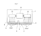
- FIG. 7 is a block diagram illustrating the schematic configuration of the printed circuit board.
- An ECU is used, for example, in a motorcycle as a vehicle, and is an ECU which controls a fuel injection timing and a fuel injection amount of a fuel injection device in a Fl system, an idle rotation speed (an idle speed control valve), and an ignition timing of an ignition mechanism.
- controlled devices such as the fuel injection device, a fuel pump, a driving device of the idle speed control valve, a driving circuit of an ignition coil, and the like are connected.
- sensors such as a crank angle sensor, an intake air temperature sensor, an intake air pressure sensor, an engine temperature sensor, a throttle sensor, and the like are connected thereto.
- the ECU includes a printed circuit board 1 illustrated in FIG. 1 , and as illustrated in FIGS. 2 to 6 , in the printed circuit board 1 , a mold resin 3 which covers and seals a part excluding a connector portion 2 , which will be described later, is provided by transfer molding.
- the printed circuit board 1 has two side surfaces, and a circuit pattern is formed and electronic components are mounted on each side surface.
- one side surface of the printed circuit board 1 is referred to as a front surface
- the other side surface is referred to as a rear surface.
- the front surface and the rear surface may be interchanged.
- the printed circuit board 1 which is a four-layer board includes, for example, two layers which are two exposed side surfaces and two inside layers. A wiring pattern is provided and the electronic components are mounted on the two exposed layers.
- the two inside layers are layers each of which includes a pattern for a power source and for the ground.
- the printed circuit board 1 has a substantially rectangular shape in which the long side is, for example, 1.1 or more times the short side. In this embodiment, the ratio therebetween is about 1.8 (about 1.6 to 2) and may also be higher.
- One side edge portion (the side edge portion on the long side) of the substantially rectangular printed circuit board 1 along the longitudinal direction serves as the connector portion 2 .
- a plurality of connection terminals 5 are provided to be arranged along the longitudinal direction of the printed circuit board 1 at equal intervals.
- semicircular cutout portions 8 are provided on the right and the left of the connector portion 2 of the printed circuit board 1 , and a section from the cutout portions 8 to the side edge of the printed circuit board 1 on the connector portion 2 side serves as the connector portion 2 and is exposed from the mold resin 3 .
- a slit 6 which is open toward the side edge of the connector portion 2 and is long along a direction perpendicular to the longitudinal direction of the printed circuit board 1 is provided.
- the width of the slit 6 along the longitudinal direction is a length in which the single connection terminal 5 can be disposed. Since the slit 6 is present, the connection terminal 5 is not disposed, and the interval between the connection terminals 5 disposed with the slit 6 interposed therebetween is longer than the other parts.
- the connector portion 2 is a plate-like member as a part of the printed circuit board 1 , and the connection terminals 5 which are respectively provided on both surfaces (front and rear surfaces) of the connector portion 2 are, for example, made of metal such as plated copper and are fixed to the front and rear surfaces of the connector portion 2 .
- the slit 6 is offset to a position which is slightly shifted from the center of the connector portion 2 in the longitudinal direction of the printed circuit board 1 .
- the mold resin 3 is molded into a thick plate shape and into a shape in which the side surfaces of the side edge portions on the short sides of the printed circuit board are curved in a substantially semicylindrical shape. Therefore, when the mold resin 3 is viewed from the front surface side on which the connector portion 2 of the printed circuit board 1 is exposed, the side surfaces on the right and the left have semicircular shapes.
- the printed circuit board is disposed at a position which is substantially the half of the thickness of the mold resin 3 .
- rib-shaped guide convex portions 12 which are guided by guide portions which are provided in the inner circumferential surface of the cover to guide the insertion of the ECU into the cover are respectively provided.
- a pair of convex portions 10 is provided on the front surface of the mold resin 3
- a pair of convex portions 11 is provided on the rear surface of the mold resin 3
- the convex portions 11 and 12 are in a state of substantially abutting on the inner circumferential surface of the cover.
- the movement (shaking) of the ECU in the cover is restricted by the convex portions 10 and 11 , the guide convex portions 12 , and the locking convex portion 7 .
- the connector portion 2 having the connection terminals 5 which are provided to be arranged along the longitudinal direction in one side edge portion along the longitudinal direction of the printed circuit board 1 is provided.
- the connection terminals 5 on one side (the right side in FIG. 7 ) in the longitudinal direction with respect to the slit 6 disposed at the substantially center portion in the longitudinal direction as a setting position of the printed circuit board 1 in the longitudinal direction are, for example, connection terminals 5 a for signal input to which wires from the above-mentioned various sensors are connected and signals from the sensors are input.
- spare connection terminals to which no wire is connected are included. There may be cases where the spare connection terminals are used for, for example, a new product in which the specifications of the ECU are changed.
- connection terminals 5 on the other side (the left side in FIG. 7 ) in the longitudinal direction with respect to the slit 6 as the setting position of the printed circuit board 1 in the longitudinal direction are, for example, connection terminals 5 b for control output for outputting control signals, driving power, or the like as control outputs to the controlled devices controlled by ECU such as the fuel injection device described above.
- connection terminals 5 b for control output spare connection terminal to which no wire is connected are also included. There may be cases where the spare connection terminals are used for, for example, a new product in which the specifications of the ECU are changed.
- a well-known microcontroller 21 for controlling the controlled device such as the above-mentioned fuel injection device is provided.
- the microcontroller 21 is disposed at substantially the center portion of one side surface (for example, the front surface) of the printed circuit board 1 in the longitudinal direction.
- the microcontroller 21 is, for example, a single-chip microcontroller which includes, for example, a CPU core and a memory such as a ROM, a RAM, or the like.
- the signals from the above-mentioned various sensors are input to the microcontroller 21 via the connection terminals 5 a for signal input, an input interface component which serves as an input interface circuit 22 , and the wiring pattern provided in the printed circuit board 1 .
- a plurality of electronic components (may also be a single electronic component) which constitute the input interface circuit 22 are disposed closer to one side (the right side in FIG. 7 ) in the longitudinal direction than substantially the center portion of the printed circuit board 1 in the longitudinal direction.
- the plurality of electronic components constituting the input interface circuit 22 convert, for example, a signal input from the outside into a form that can be input from the input terminal of the microcontroller 21 .
- the input interface electronic components basically treat a signal having a low voltage of 0.5 V or the like, and thus operate with low power without requiring high current.
- control signals for controlling the controlled devices or the driving power for driving the controlled devices are output from the connection terminals 5 a for control output to the controlled devices via an output interface electronic component which serves as an output interface circuit 23 and the wiring pattern provided in the printed circuit board 1 from the microcontroller 21 .
- a plurality of electronic components which constitute the output interface circuit 23 are disposed closer to the other side (the left side in FIG. 7 ) in the longitudinal direction than substantially the center portion of the printed circuit board 1 in the longitudinal direction.
- the electronic components constituting the output interface circuit 23 output the control signals or the driving current corresponding to the controlled devices on the basis of the control signals output from the microcontroller.
- the output current may approximately, for example, 2 amps depending on the case.
- the first layer or inside layer 32 provided with the above-described ground to which the ground terminal of the input interface component as the input interface circuit 22 is connected, and the second layer or inside layer 33 provided with the ground to which the ground terminal of the output interface component as the output interface circuit 23 is connected are different layers from each other.
- the electronic components can be mounted on both the front surface layer 31 and the rear surface layer 34 .
- the microcontroller 21 is mounted on the front surface layer 31
- the input interface component and the output interface component are mounted as described above, and even on the rear surface layer 34 , the input interface component and the output interface component are separately disposed on one side and on the other side in the longitudinal direction as described above.
- a temperature increase due to heat generation and a noise amount on the output interface circuit 23 side which treats relatively high current are greater than those on the input interface circuit 22 , and this has a possibility of adversely affecting the input interface side.
- the region in which the connection terminals 5 a on the input side, the wiring pattern on the input side on the board, and the electronic components (the input interface circuit 22 ) on the input side are disposed and the region in which the connection terminals 5 b on the output side, the wiring pattern on the output side on the board, and the electronic components (the output interface circuit 23 ) on the output side are disposed are separated from each other. Therefore, the input side can be inhibited from being adversely affected by heat or noise on the output side.
- the microcontroller including the input and output terminals is disposed at substantially the center portion in the longitudinal direction thereof, and the wiring pattern, the electronic components on the input side, the connection terminals 5 a on the input side which are connected to the input terminal side of the microcontroller 21 and the wiring pattern, the electronic components on the output side, and the connection terminals 5 b on the output side which are connected to the output terminal side of the microcontroller 21 are separately disposed on one side and the other side with respect to substantially the center of the printed circuit board 1 in the longitudinal direction. Therefore, these can be efficiently arranged, thus the wires are prevented from being lengthened due to the arrangement of the electronic components, thereby shortening the wires of the wiring pattern.
- the printed circuit board 1 which is the four-layer board, since the inside layer provided with the ground to which the ground terminal of the input interface component is connected and the inside layer provided with the ground to which the ground terminal of the output interface component is connected are different layers from each other, the input side can be prevented from being adversely affected by noise or heat on the output side.
- the connector portion 2 is provided in the side edge portion on the long side of the printed circuit board 1 along the longitudinal direction, compared to a case where the connector portion is provided in the side edge portion on the short side, a larger number of connection terminals 5 can be provided.
- the connector portion 2 having the same form as that of the current status can be used. Accordingly, even in the new product in which the number of necessary connection terminals is increased, as the connector portion 2 and the vehicle side connector connected to the connector portion 2 , components having the same shapes as those of an old product can be used. Therefore, the connector portion 2 and the connector connected to the connector portion 2 do not need to be newly designed or a part of a manufacturing apparatus does not need to be changed, thereby achieving a reduction in cost.
- the length of the connector portion 2 connected to the vehicle side connector is longer than the length of the ECU along a direction further away from the connector, and thus a structure which is less likely to be affected by vibration or impact can be achieved.
- the part of the printed circuit board 1 excluding the connector portion 2 is covered with the mold resin and thus the ECU becomes heavy, by shortening the length of the ECU which extends from the connector portion 2 as described above, stress applied to the connection portion between the connector portion 2 and the vehicle side connector is reduced at the time of receiving vibration or impact, and thus the connection portion can be prevented from receiving a high load.
- the ECU can be used in engine control of, in addition to the vehicle, for example, various general-purpose machines such as a mower, a chainsaw, an agrochemical sprayer, and a private power generator.
- various general-purpose machines such as a mower, a chainsaw, an agrochemical sprayer, and a private power generator.
Applications Claiming Priority (3)
| Application Number | Priority Date | Filing Date | Title |
|---|---|---|---|
| JP2012125515A JP6257881B2 (ja) | 2012-05-31 | 2012-05-31 | エンジンコントロールユニット |
| JP2012-125515 | 2012-05-31 | ||
| PCT/JP2013/064696 WO2013180091A1 (ja) | 2012-05-31 | 2013-05-28 | エンジンコントロールユニット |
Related Parent Applications (1)
| Application Number | Title | Priority Date | Filing Date |
|---|---|---|---|
| PCT/JP2013/064696 Continuation WO2013180091A1 (ja) | 2012-05-31 | 2013-05-28 | エンジンコントロールユニット |
Publications (2)
| Publication Number | Publication Date |
|---|---|
| US20150116955A1 US20150116955A1 (en) | 2015-04-30 |
| US9549483B2 true US9549483B2 (en) | 2017-01-17 |
Family
ID=49673285
Family Applications (1)
| Application Number | Title | Priority Date | Filing Date |
|---|---|---|---|
| US14/554,735 Expired - Fee Related US9549483B2 (en) | 2012-05-31 | 2014-11-26 | Engine control unit |
Country Status (8)
| Country | Link |
|---|---|
| US (1) | US9549483B2 (zh) |
| JP (1) | JP6257881B2 (zh) |
| CN (1) | CN104411546B (zh) |
| BR (1) | BR112014029771A2 (zh) |
| IN (1) | IN2014DN10155A (zh) |
| MY (1) | MY168453A (zh) |
| PH (1) | PH12014502636B1 (zh) |
| WO (1) | WO2013180091A1 (zh) |
Cited By (3)
| Publication number | Priority date | Publication date | Assignee | Title |
|---|---|---|---|---|
| US10535938B2 (en) | 2017-03-10 | 2020-01-14 | Tag-Connet, Llc | Side-edge connector system providing electrical connection between devices in a manner which minimizes dedicated connection space |
| US11362448B2 (en) | 2020-06-01 | 2022-06-14 | Tag-Connect, Llc | Connector having latching pins that change angle for mounting to a circuit board |
| DE102020133289A1 (de) | 2020-12-14 | 2022-06-15 | Endress+Hauser Wetzer Gmbh+Co. Kg | Elektronikeinheit |
Families Citing this family (5)
| Publication number | Priority date | Publication date | Assignee | Title |
|---|---|---|---|---|
| DE102016216997A1 (de) * | 2016-03-29 | 2017-10-05 | Continental Teves Ag & Co. Ohg | Fahrzeugkommunikationsmodul |
| JP6965767B2 (ja) * | 2018-01-23 | 2021-11-10 | 株式会社デンソー | 車載通信システム |
| JP7425615B2 (ja) | 2020-02-05 | 2024-01-31 | マツダ株式会社 | 車両用制御システム |
| JP2022044380A (ja) * | 2020-09-07 | 2022-03-17 | 株式会社デンソー | 電子装置 |
| CN114797251A (zh) * | 2022-04-30 | 2022-07-29 | 厦门华最灌溉设备科技有限公司 | 一种彩色显示屏自清洗叠片过滤系统控制器 |
Citations (12)
| Publication number | Priority date | Publication date | Assignee | Title |
|---|---|---|---|---|
| JPH05206419A (ja) | 1992-01-30 | 1993-08-13 | Nec Ic Microcomput Syst Ltd | 半導体集積回路装置 |
| JP2000183541A (ja) | 1998-12-11 | 2000-06-30 | Toshiba Iyo System Engineering Kk | 多層プリント基板 |
| JP2001025165A (ja) | 1999-07-06 | 2001-01-26 | Hitachi Ltd | 乗物の電力供給装置及び集約配線装置 |
| US6233153B1 (en) * | 1994-11-08 | 2001-05-15 | Temic Telefunken Microelectronic Gmbh | Subassembly having a housing with an integral electrical plug unit |
| US6301104B1 (en) * | 1999-07-09 | 2001-10-09 | Friendtech Computer Co., Ltd. | Interface card-type motherboard for a computer |
| US20020162829A1 (en) * | 1999-10-12 | 2002-11-07 | Weber Joseph M. | Thermally controlled circuit using planar resistive elements |
| US20040105240A1 (en) * | 2000-05-10 | 2004-06-03 | Rambus Inc. | Multiple channel modules and bus systems using same |
| US7254038B2 (en) * | 2005-04-21 | 2007-08-07 | Barracuda Networks, Inc. | Low profile expansion card for a system |
| JP2008202484A (ja) | 2007-02-20 | 2008-09-04 | Mikuni Corp | 電子制御装置及びフィードバック制御方法 |
| US20130073768A1 (en) * | 2011-09-15 | 2013-03-21 | Hon Hai Precision Industry Co., Ltd. | Expansion card and motherboard for supporting the expansion card |
| US8423695B2 (en) * | 2005-01-19 | 2013-04-16 | Broadcom Corporation | Dual PCI-X/PCI-E card |
| US20130170128A1 (en) * | 2011-12-29 | 2013-07-04 | Hon Hai Precision Industry Co., Ltd. | Motherboard |
Family Cites Families (7)
| Publication number | Priority date | Publication date | Assignee | Title |
|---|---|---|---|---|
| DE59701895D1 (de) * | 1996-09-19 | 2000-07-20 | Siemens Ag | Airbag-steuergerät |
| JPH10145013A (ja) * | 1996-11-08 | 1998-05-29 | Denso Corp | プリント配線基板 |
| JPH11274672A (ja) * | 1998-03-19 | 1999-10-08 | Denso Corp | 制御回路基板及び車両用電子制御装置 |
| JP2005294528A (ja) * | 2004-03-31 | 2005-10-20 | Seiko Epson Corp | 回路基板及び該回路基板におけるノイズの低減方法 |
| JP4478007B2 (ja) * | 2004-12-16 | 2010-06-09 | 日立オートモティブシステムズ株式会社 | 電子回路装置及びその製造方法 |
| ATE452052T1 (de) * | 2007-05-21 | 2010-01-15 | Magneti Marelli Spa | Elektronische steuereinheit mit erweiterten blöcken |
| JP5063572B2 (ja) * | 2008-12-04 | 2012-10-31 | 三菱電機株式会社 | 車載電子制御装置 |
-
2012
- 2012-05-31 JP JP2012125515A patent/JP6257881B2/ja active Active
-
2013
- 2013-05-28 MY MYPI2014703510A patent/MY168453A/en unknown
- 2013-05-28 WO PCT/JP2013/064696 patent/WO2013180091A1/ja active Application Filing
- 2013-05-28 IN IN10155DEN2014 patent/IN2014DN10155A/en unknown
- 2013-05-28 CN CN201380027878.8A patent/CN104411546B/zh active Active
- 2013-05-28 BR BR112014029771A patent/BR112014029771A2/pt not_active Application Discontinuation
-
2014
- 2014-11-25 PH PH12014502636A patent/PH12014502636B1/en unknown
- 2014-11-26 US US14/554,735 patent/US9549483B2/en not_active Expired - Fee Related
Patent Citations (12)
| Publication number | Priority date | Publication date | Assignee | Title |
|---|---|---|---|---|
| JPH05206419A (ja) | 1992-01-30 | 1993-08-13 | Nec Ic Microcomput Syst Ltd | 半導体集積回路装置 |
| US6233153B1 (en) * | 1994-11-08 | 2001-05-15 | Temic Telefunken Microelectronic Gmbh | Subassembly having a housing with an integral electrical plug unit |
| JP2000183541A (ja) | 1998-12-11 | 2000-06-30 | Toshiba Iyo System Engineering Kk | 多層プリント基板 |
| JP2001025165A (ja) | 1999-07-06 | 2001-01-26 | Hitachi Ltd | 乗物の電力供給装置及び集約配線装置 |
| US6301104B1 (en) * | 1999-07-09 | 2001-10-09 | Friendtech Computer Co., Ltd. | Interface card-type motherboard for a computer |
| US20020162829A1 (en) * | 1999-10-12 | 2002-11-07 | Weber Joseph M. | Thermally controlled circuit using planar resistive elements |
| US20040105240A1 (en) * | 2000-05-10 | 2004-06-03 | Rambus Inc. | Multiple channel modules and bus systems using same |
| US8423695B2 (en) * | 2005-01-19 | 2013-04-16 | Broadcom Corporation | Dual PCI-X/PCI-E card |
| US7254038B2 (en) * | 2005-04-21 | 2007-08-07 | Barracuda Networks, Inc. | Low profile expansion card for a system |
| JP2008202484A (ja) | 2007-02-20 | 2008-09-04 | Mikuni Corp | 電子制御装置及びフィードバック制御方法 |
| US20130073768A1 (en) * | 2011-09-15 | 2013-03-21 | Hon Hai Precision Industry Co., Ltd. | Expansion card and motherboard for supporting the expansion card |
| US20130170128A1 (en) * | 2011-12-29 | 2013-07-04 | Hon Hai Precision Industry Co., Ltd. | Motherboard |
Non-Patent Citations (1)
| Title |
|---|
| International Search Report mailed Aug. 13, 2013, in corresponding International Application No. PCT/JP2013/064696. |
Cited By (3)
| Publication number | Priority date | Publication date | Assignee | Title |
|---|---|---|---|---|
| US10535938B2 (en) | 2017-03-10 | 2020-01-14 | Tag-Connet, Llc | Side-edge connector system providing electrical connection between devices in a manner which minimizes dedicated connection space |
| US11362448B2 (en) | 2020-06-01 | 2022-06-14 | Tag-Connect, Llc | Connector having latching pins that change angle for mounting to a circuit board |
| DE102020133289A1 (de) | 2020-12-14 | 2022-06-15 | Endress+Hauser Wetzer Gmbh+Co. Kg | Elektronikeinheit |
Also Published As
| Publication number | Publication date |
|---|---|
| JP6257881B2 (ja) | 2018-01-10 |
| CN104411546A (zh) | 2015-03-11 |
| PH12014502636A1 (en) | 2015-01-26 |
| WO2013180091A1 (ja) | 2013-12-05 |
| IN2014DN10155A (zh) | 2015-08-21 |
| BR112014029771A2 (pt) | 2017-06-27 |
| MY168453A (en) | 2018-11-09 |
| JP2013251415A (ja) | 2013-12-12 |
| US20150116955A1 (en) | 2015-04-30 |
| PH12014502636B1 (en) | 2015-01-26 |
| CN104411546B (zh) | 2016-11-09 |
Similar Documents
| Publication | Publication Date | Title |
|---|---|---|
| US9549483B2 (en) | Engine control unit | |
| US6737863B2 (en) | Rotation detecting device and method of producing same | |
| JP5130110B2 (ja) | 電気接続箱 | |
| DE102012200390B4 (de) | Sensormodul | |
| JP4973053B2 (ja) | 電子装置 | |
| CN103875131A (zh) | 具有插头壳体的用于机动车的控制器 | |
| US7004009B2 (en) | Knocking sensor for internal combustion engine and manufacturing method of the same | |
| CN113490806A (zh) | 变速器壳体 | |
| JP5503483B2 (ja) | エンジン制御装置 | |
| JP6128766B2 (ja) | 電子部品実装基板 | |
| WO2013180092A1 (ja) | エンジンコントロールユニット | |
| JP5622415B2 (ja) | ジョイントコネクタ | |
| US9019716B2 (en) | Plate member, bus bar and electric junction box having the bus bar | |
| JP2007292043A (ja) | 電子スロットル装置 | |
| US20160126714A1 (en) | Housing for electronic circuit unit | |
| JP2013249780A (ja) | エンジンコントロールユニット | |
| JP2004120838A (ja) | 電子制御ユニット及び電子制御ユニット製造方法 | |
| JP2015090744A (ja) | バッテリー状態検知装置およびバッテリーポスト端子 | |
| JP2008057434A (ja) | 内燃機関用防水形回路ユニット | |
| JP5303533B2 (ja) | スロットルボディに対する回路基板の取付構造 | |
| JP2004120837A (ja) | 電子制御ユニット及び電子制御ユニット製造方法 | |
| US20240063569A1 (en) | Joint Connector and Method for Manufacturing Joint Connector | |
| JP2008034671A (ja) | 配線基板およびそれを備えた鞍乗型車両 | |
| JP2012054017A (ja) | 電子装置 | |
| CN106024271A (zh) | 制动控制装置用扼流圈 |
Legal Events
| Date | Code | Title | Description |
|---|---|---|---|
| AS | Assignment |
Owner name: MIKUNI CORPORATION, JAPAN Free format text: ASSIGNMENT OF ASSIGNORS INTEREST;ASSIGNORS:TSUJI, ICHIRO;YAMAZAKI, RYUICHI;KOGA, YOSHITAKA;REEL/FRAME:035194/0781 Effective date: 20150219 |
|
| STCF | Information on status: patent grant |
Free format text: PATENTED CASE |
|
| FEPP | Fee payment procedure |
Free format text: MAINTENANCE FEE REMINDER MAILED (ORIGINAL EVENT CODE: REM.); ENTITY STATUS OF PATENT OWNER: LARGE ENTITY |
|
| LAPS | Lapse for failure to pay maintenance fees |
Free format text: PATENT EXPIRED FOR FAILURE TO PAY MAINTENANCE FEES (ORIGINAL EVENT CODE: EXP.); ENTITY STATUS OF PATENT OWNER: LARGE ENTITY |
|
| STCH | Information on status: patent discontinuation |
Free format text: PATENT EXPIRED DUE TO NONPAYMENT OF MAINTENANCE FEES UNDER 37 CFR 1.362 |
|
| FP | Lapsed due to failure to pay maintenance fee |
Effective date: 20210117 |