US9508750B2 - Thin film transistor substrate and method for manufacturing the same - Google Patents
Thin film transistor substrate and method for manufacturing the same Download PDFInfo
- Publication number
- US9508750B2 US9508750B2 US14/552,860 US201414552860A US9508750B2 US 9508750 B2 US9508750 B2 US 9508750B2 US 201414552860 A US201414552860 A US 201414552860A US 9508750 B2 US9508750 B2 US 9508750B2
- Authority
- US
- United States
- Prior art keywords
- electrode
- gate
- source
- contact hole
- terminal
- Prior art date
- Legal status (The legal status is an assumption and is not a legal conclusion. Google has not performed a legal analysis and makes no representation as to the accuracy of the status listed.)
- Active
Links
Images


Classifications
-
- H01L27/124—
-
- H01L21/47—
-
- H01L27/1225—
-
- H01L27/1288—
-
- H01L29/66969—
-
- H—ELECTRICITY
- H10—SEMICONDUCTOR DEVICES; ELECTRIC SOLID-STATE DEVICES NOT OTHERWISE PROVIDED FOR
- H10D—INORGANIC ELECTRIC SEMICONDUCTOR DEVICES
- H10D86/00—Integrated devices formed in or on insulating or conducting substrates, e.g. formed in silicon-on-insulator [SOI] substrates or on stainless steel or glass substrates
- H10D86/01—Manufacture or treatment
- H10D86/021—Manufacture or treatment of multiple TFTs
- H10D86/0231—Manufacture or treatment of multiple TFTs using masks, e.g. half-tone masks
-
- H—ELECTRICITY
- H10—SEMICONDUCTOR DEVICES; ELECTRIC SOLID-STATE DEVICES NOT OTHERWISE PROVIDED FOR
- H10D—INORGANIC ELECTRIC SEMICONDUCTOR DEVICES
- H10D86/00—Integrated devices formed in or on insulating or conducting substrates, e.g. formed in silicon-on-insulator [SOI] substrates or on stainless steel or glass substrates
- H10D86/40—Integrated devices formed in or on insulating or conducting substrates, e.g. formed in silicon-on-insulator [SOI] substrates or on stainless steel or glass substrates characterised by multiple TFTs
- H10D86/421—Integrated devices formed in or on insulating or conducting substrates, e.g. formed in silicon-on-insulator [SOI] substrates or on stainless steel or glass substrates characterised by multiple TFTs having a particular composition, shape or crystalline structure of the active layer
- H10D86/423—Integrated devices formed in or on insulating or conducting substrates, e.g. formed in silicon-on-insulator [SOI] substrates or on stainless steel or glass substrates characterised by multiple TFTs having a particular composition, shape or crystalline structure of the active layer comprising semiconductor materials not belonging to the Group IV, e.g. InGaZnO
-
- H—ELECTRICITY
- H10—SEMICONDUCTOR DEVICES; ELECTRIC SOLID-STATE DEVICES NOT OTHERWISE PROVIDED FOR
- H10D—INORGANIC ELECTRIC SEMICONDUCTOR DEVICES
- H10D86/00—Integrated devices formed in or on insulating or conducting substrates, e.g. formed in silicon-on-insulator [SOI] substrates or on stainless steel or glass substrates
- H10D86/40—Integrated devices formed in or on insulating or conducting substrates, e.g. formed in silicon-on-insulator [SOI] substrates or on stainless steel or glass substrates characterised by multiple TFTs
- H10D86/441—Interconnections, e.g. scanning lines
-
- H—ELECTRICITY
- H10—SEMICONDUCTOR DEVICES; ELECTRIC SOLID-STATE DEVICES NOT OTHERWISE PROVIDED FOR
- H10D—INORGANIC ELECTRIC SEMICONDUCTOR DEVICES
- H10D86/00—Integrated devices formed in or on insulating or conducting substrates, e.g. formed in silicon-on-insulator [SOI] substrates or on stainless steel or glass substrates
- H10D86/40—Integrated devices formed in or on insulating or conducting substrates, e.g. formed in silicon-on-insulator [SOI] substrates or on stainless steel or glass substrates characterised by multiple TFTs
- H10D86/60—Integrated devices formed in or on insulating or conducting substrates, e.g. formed in silicon-on-insulator [SOI] substrates or on stainless steel or glass substrates characterised by multiple TFTs wherein the TFTs are in active matrices
-
- H—ELECTRICITY
- H10—SEMICONDUCTOR DEVICES; ELECTRIC SOLID-STATE DEVICES NOT OTHERWISE PROVIDED FOR
- H10D—INORGANIC ELECTRIC SEMICONDUCTOR DEVICES
- H10D99/00—Subject matter not provided for in other groups of this subclass
-
- H—ELECTRICITY
- H10—SEMICONDUCTOR DEVICES; ELECTRIC SOLID-STATE DEVICES NOT OTHERWISE PROVIDED FOR
- H10P—GENERIC PROCESSES OR APPARATUS FOR THE MANUFACTURE OR TREATMENT OF DEVICES COVERED BY CLASS H10
- H10P14/00—Formation of materials, e.g. in the shape of layers or pillars
- H10P14/60—Formation of materials, e.g. in the shape of layers or pillars of insulating materials
- H10P14/68—Organic materials, e.g. photoresists
Definitions
- the present invention relates to a TFT active matrix substrate (hereinafter referred to as “TFT substrate”) in a liquid crystal display that employs the fringe field switching (FFS) mode in which liquid crystals are held between the TFT substrate including a thin film transistor (TFT) as a switching device and a counter substrate and to a method for manufacturing the TFT substrate.
- TFT substrate TFT active matrix substrate
- FFS fringe field switching
- the display modes of liquid crystal displays are broadly divided into the twisted nematic (TN) mode and the transverse electric field mode typified by the in-plane switching (IPS) mode (IPS is a registered trademark) and the FFS mode.
- TN twisted nematic
- IPS in-plane switching
- FFS field-plane switching
- the liquid crystal displays in the transverse electric field mode have the feature of providing the wide viewing angle and the high contrast.
- the IPS mode is a display mode in which displaying is performed by applying a transverse electric field onto the liquid crystals sandwiched between opposed substrates.
- the pixel electrodes and the common electrodes onto which the transverse electric field is applied are provided in the same layer. Thus, liquid crystal molecules positioned right above the pixel electrodes cannot be sufficiently driven, which reduces the transmittance.
- the pixel electrodes and the common electrodes are disposed on the insulating film (planarization insulating film) that has been leveled, being opposed to one another via the interlayer insulating film.
- an oblique field (fringe field) is generated, allowing the transverse electric field to be applied onto the liquid crystal molecules including the ones right above the pixel electrodes, so that the liquid crystal molecules can be sufficiently driven. Therefore, the FFS mode provides a transmittance higher than that of the IPS mode.
- the liquid crystal displays are required to attain a higher aperture ratio and a further reduction in power consumption.
- the FFS-mode TFT substrate that includes a thick planarization insulating film is proposed in, for example, Japanese Patent Application Laid-Open No. 2009-128397, Japanese Patent Application Laid-Open No. 2009-133954, and Japanese Patent Application Laid-Open No. 2009-151285.
- the FFS-mode TFT substrate described above a thick planarization film is formed above the common wirings, the source wirings, and the TFT elements, whereby the parasitic capacitance of each signal line is reduced, which can suppress the power consumption.
- the upper surface of the TFT substrate can be planarized by burying the steps caused by the respective wirings. This can eliminate the irregularities in the liquid crystal alignment that have been generated in the step portion, reducing the region that does not contribute to the displaying. The aperture ratio is thus improved.
- the pixel electrodes and the signal lines are disposed to be apart from each other, to thereby eliminate the effects of electric fields generated by the signal line.
- the pixel electrodes can be formed to overlap the signal lines. Consequently, the pixel electrodes are extended, whereby the pixel aperture ratio can be increased.
- the liquid crystals are driven by the fringe field generated between the pixel electrodes (or the counter electrodes) that are provided in the upper layer and have slits and the counter electrodes (or the pixel electrodes) disposed in the layer below the pixel electrodes via the interlayer insulating film.
- the pixel electrodes and the counter electrodes are formed of a transparent conductive film based on an oxide such as indium tin oxide (ITO) containing indium oxide and tin oxide or InZnO containing indium oxide and zinc oxide, so that the pixel aperture ratio can be prevented from decreasing.
- ITO indium tin oxide
- ITO indium tin oxide
- InZnO indium oxide and zinc oxide
- the pixel electrodes and the counter electrodes form the storage capacitance. Therefore, unlikely to the liquid crystal displays in the TN mode, the pattern of the storage capacitance does not need to be separately formed in the pixels. Thus, a high pixel aperture ratio can be provided.
- amorphous silicon (Si) has been generally used as the channel layer of the semiconductor.
- the main reasons for this are as follows.
- Amorphous silicon owing to its amorphousness, can be formed into a film having excellent uniformity of properties even on a large-area substrate.
- amorphous silicon can be formed into a film at a relatively low temperature.
- the film can be formed even on the low-priced glass substrate that has poor heat resistance. Therefore, amorphous silicon is well suited for the liquid crystal displays for use in the common televisions.
- An amorphous-state film having excelling uniformity can be stably provided by optimizing the composition of the oxide semiconductor.
- the oxide semiconductor has the mobility higher than that of the conventional amorphous silicon, thus being advantageous in providing small-sized and high-performance TFT elements. Therefore, the oxide semiconductor film is advantageous in providing a FFS-mode TFT substrate that has a higher pixel aperture ratio if the film is used in the TFT element of the FFS-mode TFT substrate that includes the planarization insulating film as described above.
- the materials based on zinc oxide (ZnO) or the materials formed of zinc oxide containing gallium oxide (Ga 2 O 3 ), indium oxide (In 2 O 3 ), tin oxide (SnO 2 ), and the like are mainly used.
- This technique is disclosed in, for example, Japanese Patent Application Laid-Open No. 2004-103957, Japanese Patent Application Laid-Open No. 2007-281409, and Kenji Nomura, et al., “Room-temperature fabrication of transparent flexible thin-film transistors using amorphous oxide semiconductors,” Nature, no. 432 (2004): 488-492.
- the formation of the TFT substrate including the TFT having a bottom-gate structure disclosed in, for example, Japanese Patent Application Laid-Open No. 2009-128397, Japanese Patent Application Laid-Open No. 2009-133954, and Japanese Patent Application Laid-Open No. 2009-151285 requires at least seven photography processes of: (1) patterning for forming a gate electrode; (2) patterning for forming a semiconductor layer; (3) patterning for forming a source electrode and a drain electrode; (4) forming a contact hole in a planarization insulating film; (5) patterning for forming a lower-layer electrode; (6) forming a contact hole in a protective insulating film; and (7) patterning for forming an upper-layer electrode.
- the present invention has an object to provide a TFT active matrix substrate (TFT substrate) that allows for a reduction in the number of photolithography processes required for the manufacturing of the TFT substrate for a liquid crystal display having a structure in which common electrodes and pixel electrodes are located on a planarization insulating film and to provide a method for manufacturing the TFT substrate.
- TFT substrate TFT active matrix substrate
- a thin film transistor substrate is a thin film transistor substrate including a matrix of a plurality of pixels.
- Each of the plurality of pixels includes: a semiconductor film located on a plurality of portions of a substrate; a thin film transistor that includes at least a gate insulating film and a gate electrode, the gate insulating film being located on a first portion of the semiconductor film on the substrate and being formed of a first insulating film, the gate electrode being located on the gate insulating film and being formed of a first conductive film; a source wiring that is formed of the first conductive film and is formed on laminated films of the semiconductor film and the first insulating film; a second insulating film covering the thin film transistor and the source wiring; a source-electrode-portion contact hole and a drain-electrode-portion contact hole that penetrate the second insulating film in a thickness direction and penetrate the gate insulating film in the thickness direction to reach the first portion of the semiconductor film; a gate-electrode-portion contact hole that penetrate
- the above-mentioned TFT substrate allows for the manufacturing of the FFS-mode TFT active matrix substrate including a planarization insulating film through six photolithography processes, so that a FFS-mode liquid crystal display having a high aperture ratio can be manufactured with increased productivity and reduced cost.
- FIG. 1 is a plan view showing a configuration of a TFT substrate according to a first preferred embodiment of the present invention
- FIG. 2 is a cross-sectional view showing the configuration of the TFT substrate according to the first preferred embodiment of the present invention
- FIG. 3 is a plan view showing a method for manufacturing the TFT substrate according to the first preferred embodiment of the present invention
- FIG. 4 is a cross-sectional view showing the method for manufacturing the TFT substrate according to the first preferred embodiment of the present invention
- FIG. 5 is a plan view showing the method for manufacturing the TFT substrate according to the first preferred embodiment of the present invention.
- FIG. 6 is a cross-sectional view showing the method for manufacturing the TFT substrate according to the first preferred embodiment of the present invention.
- FIG. 7 is a plan view showing the method for manufacturing the TFT substrate according to the first preferred embodiment of the present invention.
- FIG. 8 is a cross-sectional view showing the method for manufacturing the TFT substrate according to the first preferred embodiment of the present invention.
- FIG. 9 is a plan view showing the method for manufacturing the TFT substrate according to the first preferred embodiment of the present invention.
- FIG. 10 is a cross-sectional view showing the method for manufacturing the TFT substrate according to the first preferred embodiment of the present invention.
- FIG. 11 is a plan view showing the method for manufacturing the TFT substrate according to the first preferred embodiment of the present invention.
- FIG. 12 is a cross-sectional view showing the method for manufacturing the TFT substrate according to the first preferred embodiment of the present invention.
- FIGS. 13, 14, 15, 16, 17, 18, and 19 are cross-sectional views showing a method for manufacturing the TFT substrate according to a first modification of the first preferred embodiment of the present invention
- FIG. 20 is a plan view showing a configuration the TFT substrate according to a second modification of the first preferred embodiment of the present invention.
- FIG. 21 is a cross-sectional view showing the configuration of the TFT substrate according to the second modification of the first preferred embodiment of the present invention.
- FIG. 22 is a plan view showing a method for manufacturing the TFT substrate according to the second modification of the first preferred embodiment of the present invention.
- FIG. 23 is a cross-sectional view showing the method for manufacturing the TFT substrate according to the second modification of the first preferred embodiment of the present invention.
- FIG. 24 is a plan view showing a configuration of the TFT substrate according to a third modification of the first preferred embodiment of the present invention.
- FIG. 25 is a cross-sectional view showing the configuration of the TFT substrate according to the third modification of the first preferred embodiment of the present invention.
- FIGS. 26, 27, 28, 29, and 30 are cross-sectional views showing a method for manufacturing the TFT substrate according to the third modification of the first preferred embodiment of the present invention.
- FIG. 31 is a plan view showing a configuration of the TFT substrate according to a second preferred embodiment of the present invention.
- FIG. 32 is a cross-sectional view showing the configuration of the TFT substrate according to the second preferred embodiment of the present invention.
- FIG. 33 is a plan view showing a method for manufacturing the TFT substrate according to the second preferred embodiment of the present invention.
- FIG. 34 is a cross-sectional view showing the method for manufacturing the TFT substrate according to the second preferred embodiment of the present invention.
- FIG. 35 is a plan view showing the method for manufacturing the TFT substrate according to the second preferred embodiment of the present invention.
- FIG. 36 is a cross-sectional view showing the method for manufacturing the TFT substrate according to the second preferred embodiment of the present invention.
- FIG. 37 is a plan view showing the method for manufacturing the TFT substrate according to the second preferred embodiment of the present invention.
- FIG. 38 is a cross-sectional view showing the method for manufacturing the TFT substrate according to the second preferred embodiment of the present invention.
- FIG. 39 is a plan view showing the method for manufacturing the TFT substrate according to the second preferred embodiment of the present invention.
- FIG. 40 is a cross-sectional view showing the method for manufacturing the TFT substrate according to the second preferred embodiment of the present invention.
- FIG. 41 is a plan view showing the method for manufacturing the TFT substrate according to the second preferred embodiment of the present invention.
- FIG. 42 is a cross-sectional view showing the method for manufacturing the TFT substrate according to the second preferred embodiment of the present invention.
- FIG. 43 is a plan view showing a configuration of the TFT substrate according to a modification of the second preferred embodiment of the present invention.
- FIG. 44 is a cross-sectional view showing the configuration of the TFT substrate according to the modification of the second preferred embodiment of the present invention.
- FIG. 45 is a plan view showing a method for manufacturing the TFT substrate according to the modification of the second preferred embodiment of the present invention.
- FIG. 46 is a cross-sectional view showing the method for manufacturing the TFT substrate according to the modification of the second preferred embodiment of the present invention.
- FIG. 47 is a plan view showing the method for manufacturing the TFT substrate according to the modification of the second preferred embodiment of the present invention.
- FIG. 48 is a cross-sectional view showing the method for manufacturing the TFT substrate according to the modification of the second preferred embodiment of the present invention.
- FIG. 49 is a cross-sectional view showing a configuration of the TFT substrate according to another modification of the second preferred embodiment of the present invention.
- FIG. 50 is a plan view showing a configuration of the TFT substrate according to a third preferred embodiment of the present invention.
- FIG. 51 is a cross-sectional view showing the configuration of the TFT substrate according to the third preferred embodiment of the present invention.
- FIG. 52 is a plan view showing a method for manufacturing the TFT substrate according to the third preferred embodiment of the present invention.
- FIG. 53 is a cross-sectional view showing the method for manufacturing the TFT substrate according to the third preferred embodiment of the present invention.
- FIG. 54 is a plan view showing the method for manufacturing the TFT substrate according to the third preferred embodiment of the present invention.
- FIG. 55 is a cross-sectional view showing the method for manufacturing the TFT substrate according to the third preferred embodiment of the present invention.
- FIG. 56 is a plan view showing the method for manufacturing the TFT substrate according to the third preferred embodiment of the present invention.
- FIG. 57 is a cross-sectional view showing the method for manufacturing the TFT substrate according to the third preferred embodiment of the present invention.
- FIG. 58 is a plan view showing the method for manufacturing the TFT substrate according to the third preferred embodiment of the present invention.
- FIG. 59 is a cross-sectional view showing the method for manufacturing the TFT substrate according to the third preferred embodiment of the present invention.
- FIG. 60 is a plan view showing the method for manufacturing the TFT substrate according to the third preferred embodiment of the present invention.
- FIG. 61 is a cross-sectional view showing the method for manufacturing the TFT substrate according to the third preferred embodiment of the present invention.
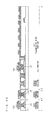
- FIG. 1 is a plan view showing a planar configuration of the pixel according to the first preferred embodiment.
- FIG. 2 is a cross-sectional view showing a cross-sectional configuration taken along the line X-X in FIG. 1 (cross-sectional configurations of a source wiring portion, a TFT portion, and a FFS transmissive pixel portion), a cross-sectional configuration taken along the line Y-Y in FIG.
- TFT substrate 100 is used for a transmissive liquid crystal display in the FFS mode.
- a plurality of gate wirings 17 (scanning signal lines) and a plurality of source wirings 6 (display signal lines) are located to perpendicularly intersect one another, a TFT element A is located near the point of intersection of both wirings, a gate electrode 4 of the TFT element A is connected to the gate wiring 17 , a source electrode 18 of the TFT element A is connected to the source wiring 6 , and a drain electrode 20 of the TFT element A is connected to a pixel electrode 21 .
- the portion that diverges from the gate wiring 17 and extends to the formation region of the TFT element A (TFT portion) is connected to the gate electrode 4 through a gate-electrode-portion contact hole 10 .
- the source electrode 18 is connected to a semiconductor film 2 through a source-electrode-portion contact hole 11 and a source-electrode connecting wiring 19 extending from the source electrode 18 is connected to the source wiring 6 through a source-wiring-portion contact hole 12 .
- the drain electrode 20 is connected to the semiconductor film 2 through a drain (pixel)-electrode-portion contact hole 13 and the pixel electrode 21 is formed to extend from the drain electrode 20 .
- the region surrounded by the adjacent gate wirings 17 and the adjacent source wirings 6 becomes a pixel region, so that the TFT substrate 100 has a configuration in which the pixel regions are arranged in matrix.
- the gate wirings 17 are disposed to extend in the horizontal direction (X direction) and the source wirings 6 are disposed to extend in the vertical direction (Y direction).
- One end of the gate wiring 17 is electrically connected to a gate terminal 7 .
- a gate-terminal-portion second contact hole 28 and a gate terminal pad 32 that is connected to the gate terminal 7 through the gate-terminal-portion second contact hole 28 are formed.
- One end of the source wiring 6 is connected to a source terminal 8 .
- a source-terminal-portion second contact hole 29 and a source terminal pad 33 that is connected to the source terminal 8 through the source-terminal-portion second contact hole 29 are formed.
- the TFT substrate 100 is formed on a transparent insulating substrate 1 made of, for example, glass.
- the TFT element A, the source wiring 6 , the gate terminal 7 , and the source terminal 8 are formed on the transparent insulating substrate 1 .
- the semiconductor film 2 and a gate insulating film 3 formed on the semiconductor film 2 are shaped into islands, having substantially the same contour pattern.
- the gate electrode 4 is formed on the gate insulating film 3 .
- the planar pattern of the gate electrode 4 of the TFT element A is formed to be smaller than the planar pattern of the semiconductor film 2 , so that the gate electrode 4 is located within the formation region of the semiconductor film 2 . This configuration allows the TFT element to be easily provided only by connecting the source electrode 18 and the drain electrode 20 to the semiconductor film 2 outside the gate electrode 4 .
- the source wiring 6 , the gate terminal 7 , and the source terminal 8 have the same layered structure as that of the TFT element A. That is, the source wiring 6 , the gate terminal 7 , and the source terminal 8 are formed on the laminated films of the semiconductor film 2 and the gate insulating film 3 , thereby forming a three-layer structure.
- a planarization insulating film 9 is formed to cover the patterns of the TFT element A, the source wiring 6 , the gate terminal 7 , and the source terminal 8 and has a plurality of contact holes formed therein. That is, the gate-electrode-portion contact hole 10 , the source-wiring-portion contact hole 12 , a gate-terminal-portion first contact hole 15 , and a source-terminal-portion first contact hole 16 that penetrate the planarization insulating film 9 in the thickness direction are formed to expose the surfaces of the gate electrode 4 , the source wiring 6 , the gate terminal 7 , and the source terminal 8 , respectively.
- the source-electrode-portion contact hole 11 and the drain (pixel)-electrode-portion contact hole 13 that penetrate the planarization insulating film 9 and the gate insulating film 3 in the thickness direction are formed to expose the surface of the semiconductor film 2 in the TFT element A.
- a conductive film is formed on the planarization insulating film 9 .
- the gate wiring 17 that is connected to the gate electrode 4 through the gate-electrode-portion contact hole 10 a gate-terminal extraction electrode 23 that is connected to the gate terminal 7 through the gate-terminal-portion first contact hole 15 , and a source-terminal extraction electrode 24 that is connected to the source terminal 8 through the source-terminal-portion first contact hole 16 are respectively formed.
- the source electrode 18 that is connected to the semiconductor film 2 through the source-electrode-portion contact hole 11 is formed.
- the source-electrode connecting wiring 19 extending from the source electrode 18 is connected to the source wiring 6 through the source-wiring-portion contact hole 12 .
- the drain electrode 20 that is connected to the semiconductor film 2 through the drain (pixel)-electrode-portion contact hole 13 is formed and the pixel electrode 21 is formed to extend from the drain electrode 20 .
- the region of the semiconductor film 2 that is sandwiched between the source electrode 18 and the drain electrode 20 and is located below the pattern of the gate electrode 4 becomes the channel region of the TFT element A.
- An interlayer insulating film 25 is formed to cover the entire upper surface of the substrate including the batch of above-mentioned electrodes on the planarization insulating film 9 .
- a counter slit electrode 31 having a comb-teeth shape in which a plurality of slits SL are provided across the entire surface thereof is formed to be opposed to the pixel electrode 21 that has a flat plate shape and becomes a lower electrode.
- the pixel electrode 21 and the counter slit electrode 31 are disposed to substantially cover the entire pixel region surrounded by two gate wirings 17 and two source wirings 6 .
- the counter slit electrode 31 is formed into, for example, a pattern that is continuous throughout the adjacent pixel regions astride the source wirings 6 .
- the counter slit electrodes 31 of the TFT substrate 100 are formed into a pattern that is continuous across the pixels in the entire image display region of the TFT active matrix substrate. Outside the image display region, the counter slit electrodes 31 are connected to signal wirings (not shown) formed in the peripheral region (frame region) of the image display region.
- the interlayer insulating film 25 has the gate-terminal-portion second contact hole 28 and the source-terminal-portion second contact hole 29 formed therein.
- the gate-terminal-portion second contact hole 28 penetrates the interlayer insulating film 25 in the thickness direction to reach the surface of the gate-terminal extraction electrode 23 .
- the source-terminal-portion second contact hole 29 penetrates the interlayer insulating film 25 in the thickness direction to reach the surface of the source-terminal extraction electrode 24 .
- the gate terminal pad 32 connected to the gate-terminal extraction electrode 23 through the contact hole 28 and the source terminal pad 33 connected to the source-terminal extraction electrode 24 through the contact hole 29 are formed.
- predetermined signals can be respectively given to the gate electrode 4 and the source electrode 18 .
- the gate terminal pad 32 and the source terminal pad 33 are formed of the same conductive film as the counter slit electrode 31 formed on the interlayer insulating film 25 .
- FIGS. 3 to 12 a method for manufacturing the TFT substrate 100 according to the first preferred embodiment is described below.
- the plan view and the cross-sectional view showing the final process correspond to FIG. 1 and FIG. 2 , respectively.
- a semiconductor film, an insulating film, and a conductive film are formed in the stated order.
- an InGaZnO-based oxide semiconductor formed of indium oxide (In 2 O 3 ) containing gallium oxide (Ga 2 O 3 ) and zinc oxide (ZnO) is used as the semiconductor film.
- An silicon oxide (SiO) film is used as the insulating film and molybdenum (Mo), which is metal, is used as the conductive film.
- a semiconductor film is firstly formed by the DC sputtering method using an InGaZnO target [In 2 O 3 .(Ga 2 O 3 ).(ZnO) 2 ] in which the atomic composition ratio of In:Ga1:Zn:O is 1:1:1:4.
- the sputtering method using argon (Ar) gas or krypton (Kr) gas that is commonly known is employed, the atomic composition ratio of oxygen is usually smaller than the stoichiometry, whereby an oxide film in an oxygen-ion deficient state (in which the composition ratio of O is less than 4 in the above example) is formed.
- Ar gas mixed with oxygen (O 2 ) gas is desirably used for sputtering.
- a sputtering was performed using Ar gas containing O 2 gas mixed at 10% by partial pressure ratio, whereby an InGaZnO-based oxide semiconductor film was formed to have a thickness of 40 nm.
- the oxide semiconductor film functions as the semiconductor film 2 in the TFT element A.
- the In—Ga—Zn—O film immediately after formation had an amorphous structure.
- an insulating film composed of SiO is formed by the plasma chemical vapor deposition (CVD) method using silane (SiH 4 ) gas and dinitrogen oxide (N 2 O) gas.
- the insulating film functions as the gate insulating film 3 in the TFT element.
- a conductive film composed of Mo is formed to have a thickness of 200 nm by the DC sputtering method using a Mo target.
- Ar gas or Kr gas that is commonly known is used as a sputtering gas.
- a photoresist pattern is formed on the laminated films of the semiconductor film, the insulating film, and the conductive film in the photolithography process, and then, the Mo film located in the top layer is firstly etched to be patterned using the photoresist pattern as a mask by wet etching in which a mixed acid (hereinafter referred to as PAN solution) including phosphoric acid, acetic acid, and nitric acid is used.
- PAN solution mixed acid
- the insulating film (SiO film) is etched to be patterned using the photoresist pattern and the patterned Mo film as a mask by dry etching in which oxygen (O 2 ) gas and a gas containing fluorine such as CHF 3 and CF 4 are used.
- the semiconductor film (InGaZnO-based oxide semiconductor film) is etched to be patterned using the photoresist pattern and the patterned Mo film and the patterned SiO film as a mask by wet etching in which a solution (hereinafter referred to as oxalic-acid based solution) mainly composed of oxalic acid (carboxylic acid) is used.
- a solution hereinafter referred to as oxalic-acid based solution mainly composed of oxalic acid (carboxylic acid) is used.
- FIG. 3 is a plan view corresponding to FIG. 1 and FIG. 4 is a cross-sectional view corresponding to FIG. 2 .
- FIG. 5 is a plan view corresponding to FIG. 1 and FIG. 6 is a cross-sectional view corresponding to FIG. 2 .
- planarization insulating film 9 is formed to cover the entire upper surface of the transparent insulating substrate 1 including the gate electrode 4 , the source wiring 6 , the gate terminal 7 , and the source terminal 8 formed by patterning. Then, a plurality of contact holes are formed.
- an acrylic organic resin material having photosensitivity is applied onto the transparent insulating substrate 1 to have a thickness of 2.0 to 3.0 ⁇ m by spin coating.
- an acrylic organic resin material having photosensitivity is applied onto the transparent insulating substrate 1 to have a thickness of 2.0 to 3.0 ⁇ m by spin coating.
- the planarization insulating film 9 may be made of an olefin-based material, a novolac-based material, a polyimide-based material, or a siloxane-based material aside from the acrylic organic resin material. These coating-type organic insulating materials have low dielectric constants, thus being capable of keeping the wiring capacitance low. The use of such a material enables the TFT substrate to be driven at low voltage, thereby contributing to a reduction in power consumption.
- the planarization insulating film 9 having photosensitivity is patterned for simultaneously forming the gate-electrode-portion contact hole 10 , the source-electrode-portion contact hole 11 , the source-wiring-portion contact hole 12 , the drain (pixel)-electrode-portion contact hole 13 , the gate-terminal-portion first contact hole 15 , and the source-terminal-portion first contact hole 16 .
- the gate insulating film 3 is exposed through the bottom of the source-electrode-portion contact hole 11 and the drain (pixel)-electrode-portion contact hole 13 . Then, only the exposed part of the gate insulating 3 is selectively etched using the planarization insulating film 9 as a mask, whereby the surface of the underlying semiconductor film 2 is exposed. Consequently, the source-electrode-portion contact hole 11 and the drain (pixel)-electrode-portion contact hole 13 that reach the semiconductor film 2 are completed. Thus, as shown in FIGS. 7 and 8 , a plurality of contact holes that penetrate the planarization insulating film 9 in the thickness direction are obtained.
- the gate insulating film 3 composed of SiO can be etched by dry etching in which oxygen (O 2 ) gas and a gas containing fluorine such as CHF 3 and CF 4 are used.
- FIG. 7 is a plan view corresponding to FIG. 1 and FIG. 8 is a cross-sectional view corresponding to FIG. 8 .
- a transparent conductive film is formed on the entire upper surface of the planarization insulating film 9 and a photoresist pattern is formed on the transparent conductive film in the fourth photolithography process.
- the above-mentioned transparent conductive film is patterned using the photoresist pattern as a mask. Consequently, the gate wiring 17 connected to the gate electrode 4 through the gate-electrode-portion contact hole 10 , the gate-terminal extraction electrode 23 connected to the gate terminal 7 through the gate-terminal-portion first contact hole 15 , and the source-terminal extraction electrode 24 connected to the source terminal 8 through the source-terminal-portion first contact hole 16 are respectively formed.
- the source electrode 18 connected to the semiconductor film 2 through the source-electrode-portion contact hole 11 is formed.
- the source-electrode connecting wiring 19 is integrally formed with the source electrode 18 .
- the source-electrode connecting wiring 19 is connected to the source wiring 6 through the source-wiring-portion contact hole 12 .
- the drain electrode 20 connected to the semiconductor film 2 through the drain (pixel)-electrode-portion contact hole 13 is also formed.
- the pixel electrode 21 that substantially covers the entire pixel region surrounded by two gate wirings 17 and two source wirings 6 is integrally formed with the drain electrode 20 .
- the region of the semiconductor film 2 that is sandwiched between the source electrode 18 and the drain electrode 20 and is located below the pattern of the gate electrode 4 becomes the channel region of the TFT element A.
- an InZnO film having a thickness of 100 nm is formed on the entire upper surface of the planarization insulating film 9 by the DC sputtering method in which an InZnO target containing indium oxide and zinc oxide is used. Then, the film is wet-etched with the oxalic-acid based solution using the photoresist pattern formed in the fourth photolithography process as a mask and is patterned into each of the above-mentioned electrodes and wirings. Consequently, as shown in FIGS.
- FIG. 9 is a plan view corresponding to FIG. 1 and FIG. 10 is a cross-sectional view corresponding to FIG. 2 .
- the interlayer insulating film 25 is formed to cover the entire upper surface of the transparent insulating substrate 1 . More specifically, for example, a silicon nitride (SiN) film having a thickness of 200 to 400 nm is formed as the interlayer insulating film 25 by the plasma CVD method.
- SiN silicon nitride
- FIG. 11 is a plan view corresponding to FIG. 1 and FIG. 12 is a cross-sectional view corresponding to FIG. 12 .
- a transparent conductive film is formed on the entire upper surface of the interlayer insulating film 25 and a photoresist pattern is formed on the transparent conductive film in the sixth photolithography process.
- the above-mentioned transparent conductive film is patterned using the photoresist pattern as a mask. Consequently, the counter slit electrode 31 having a comb-teeth shape in which the plurality of slits SL are provided across the entire surface thereof is formed.
- the counter slit electrode 31 is disposed to substantially cover the entire pixel region surrounded by two gate wirings 17 and two source wirings 6 such that the counter slit electrode 31 is opposed to the pixel electrode 21 that becomes the lower electrode.
- the counter slit electrode 31 is formed into a pattern that is continuous to the counter slit electrodes 31 in the adjacent pixel regions astride the source wirings 6 .
- the counter slit electrodes 31 are formed into a pattern that is continuous across the pixels in the entire image display region of the TFT substrate 100 . Outside the image display region, the counter slit electrodes 31 are connected to the signal wirings (not shown) formed in the frame region.
- the gate terminal pad 32 and the source terminal pad 33 are formed.
- the gate terminal pad 32 is connected to the gate-terminal extraction electrode 23 through the gate-terminal-portion second contact hole 28 formed through the interlayer insulating film 25 .
- the source terminal pad 33 is connected to the source-terminal extraction electrode 24 through the source-terminal-portion second contact hole 29 formed through the interlayer insulating film 25 .
- an InZnO film having a thickness of 100 nm is formed on the entire upper surface of the interlayer insulating film 25 by the DC sputtering method in which an InZnO target containing indium oxide and zinc oxide is used. Then, the film is wet-etched with the oxalic-acid based solution using the photoresist pattern formed in the sixth photolithography process as a mask and is patterned into each of the above-mentioned electrodes and wirings. Consequently, the counter slit electrode 31 , the gate terminal pad 32 , and the source terminal pad 33 that are shown in FIGS. 1 and 2 are simultaneously obtained.
- the counter slit electrode 31 is formed of the transparent conductive film, so that the transmitted display light in the pixel region is not blocked. This prevents the aperture ratio from lowering, whereby the aperture ratio can be kept high.
- the TFT substrate 100 shown in FIGS. 1 and 2 can be obtained through the six photolithography processes.
- an alignment film and spacers are formed on the surface of the completed TFT substrate 100 .
- the alignment film is provided to align liquid crystals and is formed of, for example, polyimide.
- a counter substrate including a color filter and an alignment film is prepared. Then, the TFT substrate 100 and the counter substrate are bonded together.
- the TFT substrate 100 and the counter substrate are bonded together with a certain gap kept therebetween by the above-mentioned spacers.
- the liquid crystals are injected into the gap to be sealed therein. That is, the liquid crystal layer is sandwiched between the TFT substrate 100 and the counter substrate.
- polarizing plates, phase difference plates, and a backlight unit are mainly disposed, thereby providing a FFS-mode liquid crystal display.
- the oxide semiconductor composed of InGaZnO is used as the semiconductor film 2 , which is not limited thereto.
- an oxide semiconductor film based on InZnO, InGaO, InSnO, ZnSnO, InSnZnO, InGaZnSnO, InAlZnO, InHfZnO, InZrZnO, InMgZnO, InYZnO, or the like may be used.
- the transparent conductive film composed of InZnO is used as the pixel electrode 21 and the counter slit electrode 31 , which is not limited thereto.
- oxide-based transparent conductive films such as films based on InSnO (ITO), GaZnO, and ZnAlO may be used.
- the oxide semiconductor is used as the channel layer of the TFT element, thereby providing the TFT substrate having high mobility, high performance, and a high aperture ratio for use in a FFS-mode liquid crystal display.
- the TFT substrate can be manufactured through the six photolithography processes, thereby reducing the manufacturing costs of the FFS-mode liquid crystal display.
- a semiconductor film 202 on the entire upper surface of the transparent insulating substrate 1 made of, for example, glass, a semiconductor film 202 , an insulating film 203 , and a conductive film 204 are formed in the stated order.
- an InGaZnO-based oxide semiconductor formed of indium oxide (In 2 O 3 ) containing gallium oxide (Ga 2 O 3 ) and zinc oxide (ZnO) is used as the semiconductor film 202 .
- a silicon oxide (SiO) film is used as the insulating film 203 and molybdenum (Mo), which is metal, is used as the conductive film 204 .
- the specific methods for manufacturing these films are the same as the methods described in the first preferred embodiment, and the description thereof is omitted.
- a photoresist 101 composed of a novolac-based positive-type photosensitive resin is applied onto the laminated films of the semiconductor film 202 , the insulating film 203 , and the conductive film 204 to have a thickness of about 1.6 ⁇ m by spin coating.
- the photomask 91 has an opening (exposure-light transmissive region) 91 a and a light-shielding portion (exposure-light shielding region) 91 b formed therein for forming the patterns of the TFT element A, the source wiring 6 , the gate terminal 7 , and the source terminal 8 .
- the opening 91 a corresponds to an exposed region 101 a through which an exposure light 92 is transmitted as it is to reach the photoresist 101 .
- the light-shielding portion 91 b corresponds to a photoresist unexposed region 101 b that blocks the exposure light.
- An exposure-light semi-transmissive region 91 c having a semi-transmissive film formed therein is formed in the regions of the photomask 91 corresponding to the both ends of the TFT element A.
- the exposure-light semi-transmissive region 91 c corresponds to a photoresist intermediate exposed region 101 c that transmits an exposure light 94 in which the intensity of the original exposure light 92 is reduced by 40 to 60%.
- the photolithography method in which the intermediate exposed region is provided as described above is hereinafter referred to as the half-tone method.
- a development is performed using an organic alkali-based developing solution that contains tetramethyl ammonium hydroxide (TMAH). Consequently, as shown in FIG. 16 , the photoresist 101 is removed except for the portions corresponding to the TFT element A, a source-wiring resist pattern 106 , a gate-terminal resist pattern 107 , and a source-terminal resist pattern 108 . At the same time, a gate-electrode resist pattern 104 having a first thickness is formed in the TFT element A.
- TMAH tetramethyl ammonium hydroxide
- a semiconductor resist pattern 102 having a second thickness that is smaller than the thickness of the unexposed region is formed in the exposed region of the TFT element A in the photoresist intermediate exposed region 101 c .
- the second film thickness of the semiconductor resist pattern 102 was about 0.4 ⁇ m.
- the conductive film 204 , the insulating film 203 , and the semiconductor film 202 are sequentially etched using the above-described resist patterns 102 , 104 , 106 , 107 , and 108 as a mask.
- the specific method for etching these films is the same as that of the first preferred embodiment, and the description thereof is omitted.
- the film thicknesses of the resist patterns are reduced overall by the O 2 ashing and the semiconductor resist pattern 102 having the smaller film thickness is completely removed. Consequently, the gate-electrode resist pattern 104 , the source-wiring resist pattern 106 , the gate-terminal resist pattern 107 , and the source-terminal resist pattern 108 having the desired thickness are formed.
- a half ashing is performed for partially leaving the resist, so that the gate-electrode resist pattern 104 , the source-wiring resist pattern 106 , the gate-terminal resist pattern 107 , and the source-terminal resist pattern 108 are left.
- the conductive film 204 that is located in the top layer and made of Mo is etched to be patterned using the above-mentioned resist patterns as a mask by wet etching in which the PAN solution is used.
- the photoresist is removed, whereby the semiconductor film 2 , the gate insulating film 3 , the gate electrode 4 , the source wiring 6 , the gate terminal 7 , and the source terminal 8 that are similar to the ones in FIG. 6 are obtained.
- two photolithography processes are required to obtain the configuration shown in FIG. 6 in the first preferred embodiment, only one process of photolithography is required in this modification.
- the manufacturing processes described in the first preferred embodiment with reference to FIGS. 7 to 12 are performed, whereby the TFT substrate 100 in the FFS mode according to the first preferred embodiment of the present invention is manufactured.
- the manufacturing method according to this modification can reduce the number of photolithography processes, whereby the TFT substrate can be manufactured through the five photolithography processes.
- a FFS-mode liquid crystal display can be manufactured with increased productivity and reduced cost.
- a configuration further including an upper-layer gate wiring that is formed in the same layer as the counter slit electrode 31 using the same transparent conductive film as the counter slit electrode 31 is described below.
- FIG. 20 is a plan view showing a planar configuration of a pixel according to a second modification
- FIG. 21 is a cross-sectional view showing a cross-sectional configuration taken along the line X-X in FIG. 20 (cross-sectional configurations of the source wiring portion, the TFT portion, and the FFS transmissive pixel portion), a cross-sectional configuration taken along the line Y-Y in FIG. 20 (a cross-sectional configuration of the gate terminal portion), and a cross-sectional configuration taken along the line Z-Z in FIG. 20 (a cross-sectional configuration of the source terminal portion).
- constituents that are the same as those of the TFT substrate 100 described with reference to FIGS. 1 and 2 are given the same reference signs, and the overlapping description is omitted.
- the portion that diverges from the gate wiring 17 and extends to the formation region of the TFT element A (TFT portion) is connected to the gate electrode 4 through the gate-electrode-portion contact hole 10 .
- a gate-electrode-portion upper-layer contact hole 26 is provided above the gate-electrode-portion contact hole 10 and an upper-layer gate wiring 30 that is connected to the gate wiring 17 through the gate-electrode-portion upper-layer contact hole 26 is formed.
- the interlayer insulating film 25 is formed to cover the entire upper surface of the transparent insulating substrate 1 . More specifically, for example, a silicon nitride (SiN) film having a thickness of 200 to 400 nm is formed as the interlayer insulating film 25 by the plasma CVD method.
- SiN silicon nitride
- a photoresist pattern is formed on the interlayer insulating film 25 in the fifth photolithography process.
- the SiN film is etched using the photoresist pattern as a mask by dry etching in which O 2 gas and a gas containing fluorine such as CF 4 and SF 6 are used, and then, the photoresist pattern is removed. Consequently, as shown in FIGS.
- the gate-terminal-portion second contact hole 28 that reaches the surface of the gate-terminal extraction electrode 23 the source-terminal-portion second contact hole 29 that reaches the surface of the source-terminal extraction electrode 24 , and the gate-electrode-portion upper-layer contact hole 26 that reaches the surface of the gate wiring 17 are formed.
- a transparent conductive film is formed on the entire upper surface of the interlayer insulating film 25 and a photoresist pattern is formed on the transparent conductive film in the sixth photolithography process.
- the above-mentioned transparent conductive film is patterned using the photoresist pattern as a mask. Consequently, the counter slit electrode 31 having a comb-teeth shape in which the plurality of slits SL are provided across the entire surface thereof is formed.
- the gate terminal pad 32 is connected to the gate-terminal extraction electrode 23 through the gate-terminal-portion second contact hole 28 formed through the interlayer insulating film 25 .
- the source terminal pad 33 is connected to the source-terminal extraction electrode 24 through the source-terminal-portion second contact hole 29 formed through the interlayer insulating film 25 .
- the upper-layer gate wiring 30 is connected to the gate wiring 17 through the gate-electrode-portion upper-layer contact hole 26 formed through the interlayer insulating film 25 . Note that the above-mentioned photoresist pattern is patterned such that the upper-layer gate wiring 30 is also formed on the gate wiring 17 .
- an InZnO film having a thickness of 100 nm is formed on the entire upper surface of the interlayer insulating film 25 by the DC sputtering method in which an InZnO target containing indium oxide and zinc oxide is used. Then, the film is wet-etched with the oxalic-acid based solution using the photoresist pattern formed in the sixth photolithography process as a mask and is patterned into each of the above-mentioned electrodes and wirings. Consequently, the counter slit electrode 31 , the gate terminal pad 32 , the source terminal pad 33 , and the upper-layer gate wiring 30 that are shown in FIGS. 20 and 21 are simultaneously obtained.
- the counter slit electrode 31 is formed of the transparent conductive film, so that the transmitted display light in the pixel region is not blocked. This prevents the aperture ratio from lowering, whereby the aperture ratio can be kept high.
- the TFT substrate 100 A according to the second modification described above has the following characteristics.
- the TFT substrate 100 A can be obtained through the six photolithography processes, similarly to the manufacturing method in the first preferred embodiment.
- the TFT substrate 100 A includes the upper-layer gate wiring 30 , whereby the gate wiring resistance is further reduced and the gate signal delay is prevented even if the substrate is included in a large panel. Thus, the display quality is improved.
- the TFT substrate 100 A includes the two-layer structure of the gate wiring 17 and the upper-layer gate wiring 30 that is formed in the same layer as the counter silt electrode 31 , providing the so-called redundant wiring. This can significantly reduce breakages of the gate wirings.
- the TFT substrate 100 A can also be manufactured through the five photolithography processes, allowing for a cost reduction. Therefore, a FFS-mode liquid crystal display can be manufactured with increased productivity and reduced cost.
- FIG. 24 is a plan view showing a planar configuration of a pixel according to a third modification
- FIG. 25 is a cross-sectional view showing a cross-sectional configuration taken along the line X-X in FIG. 24 (cross-sectional configurations of the source wiring portion, the TFT portion, and the FFS transmissive pixel portion), a cross-sectional configuration taken along the line Y-Y in FIG. 24 (a cross-sectional configuration of the gate terminal portion), and a cross-sectional configuration taken along the line Z-Z in FIG. 24 (a cross-sectional configuration of the source terminal portion).
- constituents that are the same as those of the TFT substrate 100 described with reference to FIGS. 1 and 2 are given the same reference signs, and the overlapping description is omitted.
- the portion that diverges from the gate wiring 17 and extends to the formation region of the TFT element A (TFT portion) is connected to the gate electrode 4 through the gate-electrode-portion contact hole 10 .
- the upper-layer gate wiring 30 is formed above the gate-electrode-portion contact hole 10 and on the gate wiring 17 .
- the gate-electrode-portion upper-layer contact hole 26 is disposed above the gate-electrode-portion contact hole 10 .
- An uppermost-layer gate wiring 34 formed of a conductive film is disposed on the upper-layer wiring 30 and on the gate terminal pad 32 .
- a transparent conductive film and a metal film are formed on the entire upper surface of the interlayer insulating film 25 in the stated order and a photoresist pattern is formed on the metal film by the half-tone method in the sixth photolithography process.
- the metal film and the transparent conductive film mentioned above are patterned using the photoresist pattern as a mask, to thereby form the counter slit electrode 31 having a comb-teeth shape, the gate terminal pad 32 , the source terminal pad 33 , and the upper-layer gate wiring 30 .
- the gate terminal pad 32 is connected to the gate-terminal extraction electrode 23 through the gate-terminal-portion second contact hole 28 formed through the interlayer insulating film 25 .
- the source terminal pad 33 is connected to the source-terminal extraction electrode 24 through the source-terminal-portion second contact hole 29 formed through the interlayer insulating film 25 .
- the upper-layer gate wiring 30 is connected to the gate wiring 17 through the gate-electrode-portion upper-layer contact hole 26 formed through the interlayer insulating film 25 . Note that a metal film is formed on these electrodes and wirings.
- the photoresist pattern that is unnecessary is removed using the photoresist pattern that has been partially left by half ashing and the metal film that is unnecessary is removed using the photoresist pattern that has been left. Consequently, the TFT substrate 100 B shown in FIGS. 24 and 25 is obtained.
- the manufacturing method described above is further described below with reference to FIGS. 26 to 30 .
- the processes described in the second modification with reference to FIG. 23 are performed, so that the gate-terminal-portion second contact hole 28 that reaches the surface of the gate-terminal extraction electrode 23 , the source-terminal-portion second contact hole 29 that reaches the surface of the source-terminal extraction electrode 24 , and the gate-electrode-portion upper-layer contact hole 26 that reaches the surface of the gate wiring 17 are formed.
- a transparent conductive film 120 is formed on the interlayer insulating film 25 and in these holes as shown in FIG. 26 .
- An InZnO film having a thickness of 100 nm is formed by the DC sputtering method in which an InZnO target containing indium oxide and zinc oxide is used, whereby the transparent conductive film 120 is obtained. Subsequently, an AlNiNd film having a thickness of 100 nm is formed on the entire upper surface of the transparent conductive film 120 by the DC magnetron sputtering method in which an AlNiNd target that is an Al alloy is used, thereby providing a metal film 121 .
- a photoresist composed of a novolac-based positive-type photosensitive resin is applied onto the metal film 121 to have a thickness of about 1.6 ⁇ m by spin coating.
- the photoresist is exposed by the half-tone method and developed, whereby a predetermined photoresist pattern is obtained.
- the predetermined photoresist pattern includes an upper-layer gate-wiring photoresist pattern 130 for patterning for forming the upper-layer gate wiring 30 , a counter-slit-electrode photoresist pattern 131 for patterning for forming the counter slit electrode 31 , a gate-terminal-pad photoresist pattern 132 for patterning for forming the gate terminal pad 32 , a source-terminal-pad photoresist pattern 133 for patterning for forming the source terminal pad 33 , and an uppermost-layer gate-wiring photoresist pattern 134 for patterning for forming the uppermost-layer gate wiring 34 .
- All of the patterns except for the uppermost-layer gate-wiring photoresist pattern 134 having a first thickness are formed into a second thickness (about 0.4 ⁇ m).
- the uppermost-layer gate-wiring photoresist pattern 134 formed inside the regions of the upper-layer gate-wiring photoresist pattern 130 and gate-terminal-pad photoresist pattern 132 is formed to have a thickness larger than that of the other patterns.
- the metal film 121 is etched with an alkali-based organic developing solution that contains tetramethyl ammonium hydroxide (TMAH) using the above-mentioned photoresist patterns as a mask. Then, the transparent conductive film 120 is etched with an oxalic-acid based solution, whereby the metal film 121 and the transparent conductive film 120 located in the regions that are not covered by the photoresist patterns are removed.
- TMAH tetramethyl ammonium hydroxide
- the photoresist is thinned by ashing in which the transparent insulating substrate 1 is entirely irradiated with oxygen (O 2 ) plasma, whereby only the uppermost-layer gate-wiring photoresist pattern 134 is left and other photoresist patterns are removed.
- oxygen O 2
- the metal film 121 is etched with above-mentioned developing solution using the uppermost-layer gate-wiring photoresist pattern 134 as a mask, thereby being patterned into the uppermost-layer gate wiring 34 on the upper-layer gate wiring 30 and on the gate terminal pad 32 . Then, the photoresist pattern is removed.
- the TFT substrate 100 B including the counter slit electrode 31 , the gate terminal pad 32 , the source terminal pad 33 , the upper-layer gate wiring 30 , and the uppermost-layer gate wiring 34 can be obtained through the six photolithography processes.
- the metal film 121 may be patterned such that the metal film 121 on the gate terminal pad 32 is deleted, whereby the uppermost-layer gate wiring 34 is not disposed on the gate terminal pad 32 .
- the metal film 121 may be left not only on the gate terminal pad 32 but also on the source terminal pad 33 , to thereby provide an uppermost-layer source wiring in the same way as the uppermost-layer gate wiring 34 .
- the metal film 121 may not be left on the gate terminal pad 32 and the metal film 121 may be alternatively left on the source terminal pad 33 , to thereby provide the uppermost-layer source wiring.
- the uppermost-layer gate wiring 34 and the wirings disposed in the same layer thereof are provided only to reduce the gate wiring resistance. Therefore, the wirings need to be formed on the layer above the gate wiring while being optionally disposed on the layer above the respective terminal portions.
- the film can be easily transformed, at the time of connection (mounting) of the wiring substrate and the integrated circuit (IC) chips for imputing signals from the outside, along the shapes of the mounted members. This can improve the connection properties, leading to an improvement in reliability.
- the terminal pads are formed of an oxide conductive film such as InZnO. This is in no way inferior in terms of improving the connection properties, leading to an improvement in reliability similarly to the above case.
- the TFT substrate 100 B according to the third modification described above has the following characteristics.
- the TFT substrate 100 B can be obtained through the six photolithography processes similarly to the manufacturing method in the first preferred embodiment.
- the TFT substrate 100 B includes the upper-layer gate wiring 30 and the uppermost-layer gate wiring 34 disposed on the gate wiring 17 , whereby the gate wiring resistance is further reduced and the gate signal delay is prevented even if the substrate is included in a large panel. Thus, the display quality is improved.
- the TFT substrate 100 B includes the three-layer structure of the gate wiring 17 , the upper-layer gate wiring 30 that is formed in the same layer as the counter silt electrode 31 , and the uppermost-layer gate wiring 34 that is formed on the upper-layer gate wiring 30 , providing the so-called redundant wiring. This can significantly reduce breakages of the gate wirings.
- the TFT substrate 100 B can also be manufactured through the five photolithography processes, allowing for a cost reduction. Therefore, a FFS-mode liquid crystal display can be manufactured with increased productivity and reduced cost.
- the counter slit electrode 31 is formed of the transparent conductive film, so that the transmitted display light in the pixel region is not blocked. This prevents the aperture ratio from lowering, whereby the aperture ratio can be kept high.
- a configuration of a TFT substrate 200 according to a second preferred embodiment is described. Note that constituents that are the same as those of the TFT substrate 100 described with reference to FIGS. 1 and 2 are given the same reference signs, and the overlapping description is omitted.
- FIG. 31 is a plan view showing a planar configuration of a pixel according to the second preferred embodiment.
- FIG. 32 is a cross-sectional view showing a cross-sectional configuration taken along the line X-X in FIG. 31 (cross-sectional configurations of the source wiring portion, the TFT portion, the FFS transmissive pixel portion, a common electrode portion, and a common-electrode connection portion), a cross-sectional configuration taken along the line Y-Y in FIG. 31 (a cross-sectional configuration of the gate terminal portion), and a cross-sectional configuration taken along the line Z-Z in FIG. 31 (a cross-sectional configuration of the source terminal portion).
- the TFT substrate 200 is used for a transmissive liquid crystal display in the FFS mode.
- a common electrode 5 is disposed to extend in a direction parallel to the gate wiring 17 in each pixel.
- the common electrode 5 is formed in the same layer as, for example, the source wiring 6 .
- a common-electrode connection-portion contact hole 14 that penetrates the planarization insulating film 9 in the thickness direction is formed.
- the common electrodes 5 that are adjacent to each other are electrically connected by an upper-layer common-electrode connecting wiring 35 that extends from the counter slit electrode 31 through the common-electrode connection-portion contact hole 14 .
- This configuration can reduce the electrical resistance of the common electrodes 5 for supplying the counter slit electrode 31 with a certain common potential.
- the substrate is applicable to a large panel.
- An Al alloy for example, AlNiNd
- Mo molybdenum
- the source wiring 6 located in the same layer as the common electrodes 5 so that the wiring resistance can be further reduced.
- FIGS. 33 to 42 a method for manufacturing the TFT substrate 200 according to the second preferred embodiment is described below.
- the plan view and the cross-sectional view showing the final process correspond to FIG. 31 and FIG. 32 , respectively.
- the transparent insulating substrate 1 made of, for example, glass, a semiconductor film, an insulating film, and a conductive film are formed in the stated order.
- the method for manufacturing these films has been described in the first preferred embodiment, and the description thereof is omitted.
- a photoresist pattern is formed on the laminated films of the semiconductor film, the insulating film, and the conductive film in the photolithography process, and then, the Mo film located in the top layer is firstly etched to be patterned using the photoresist pattern as a mask by wet etching in which the PAN solution is used.
- the insulating film (SiO film) is etched to be patterned using the photoresist pattern and the patterned Mo film as a mask by dry etching in which oxygen (O 2 ) gas and a gas containing fluorine such as CHF 3 and CF 4 are used.
- the semiconductor film (InGaZnO-based oxide semiconductor film) is etched to be patterned using the photoresist pattern, the patterned Mo film, and the patterned SiO film as a mask by wet etching in which the oxalic-acid based solution is used.
- FIG. 33 is a plan view corresponding to FIG. 31 and FIG. 34 is a cross-sectional view corresponding to FIG. 32 .
- FIG. 35 is a plan view corresponding to FIG. 31 and FIG. 36 is a cross-sectional view corresponding to FIG. 32 .
- planarization insulating film 9 is formed to cover the entire upper surface of the transparent insulating substrate 1 including the gate electrode 4 , the common electrode 5 , the source wiring 6 , the gate terminal 7 , and the source terminal 8 formed by patterning. Then, a plurality of contact holes are formed.
- the method for manufacturing the planarization insulating film 9 has been described in the first preferred embodiment, and the description thereof is omitted.
- the planarization insulating film 9 having photosensitivity is patterned for simultaneously forming the gate-electrode-portion contact hole 10 , the source-electrode-portion contact hole 11 , the source-wiring-portion contact hole 12 , the drain (pixel)-electrode-portion contact hole 13 , the common-electrode connection-portion contact hole, the gate-terminal-portion first contact hole 15 , and the source-terminal-portion first contact hole 16 .
- the gate insulating film 3 is exposed through the bottom of the source-electrode-portion contact hole 11 and the drain (pixel)-electrode-portion contact hole 13 . Then, only the exposed part of the gate insulating 3 is selectively etched using the planarization insulating film 9 as a mask, whereby the surface of the underlying semiconductor film 2 is exposed. Consequently, the source-electrode-portion contact hole 11 and the drain (pixel)-electrode-portion contact hole 13 that reach the semiconductor film 2 are completed. Thus, as shown in FIGS. 37 and 38 , a plurality of contact holes that penetrate the planarization insulating film 9 in the thickness direction are obtained.
- the gate insulating film 3 composed of SiO can be etched by dry etching in which oxygen (O 2 ) gas and a gas containing fluorine such as CHF 3 and CF 4 are used.
- FIG. 37 is a plan view corresponding to FIG. 31 and FIG. 38 is a cross-sectional view corresponding to FIG. 38 .
- a transparent conductive film is formed on the entire upper surface of the planarization insulating film 9 and a photoresist pattern is formed on the transparent conductive film in the fourth photolithography process.
- the above-mentioned transparent conductive film is patterned using the photoresist pattern as a mask. Consequently, the gate wiring 17 connected to the gate electrode 4 through the gate-electrode-portion contact hole 10 , the gate-terminal extraction electrode 23 connected to the gate terminal 7 through the gate-terminal-portion first contact hole 15 , and the source-terminal extraction electrode 24 connected to the source terminal 8 through the source-terminal-portion first contact hole 16 are respectively formed.
- the source electrode 18 connected to the semiconductor film 2 through the source-electrode-portion contact hole 11 is formed.
- the source-electrode connecting wiring 19 is integrally formed with the source electrode 18 .
- the source-electrode connecting wiring 19 is connected to the source wiring 6 through the source-wiring-portion contact hole 12 .
- the drain electrode 20 connected to the semiconductor film 2 through the drain (pixel)-electrode-portion contact hole 13 is also formed.
- the pixel electrode 21 that substantially covers the entire pixel region surrounded by two gate wirings 17 and two source wirings 6 is integrally formed with the drain electrode 20 .
- the region of the semiconductor film 2 that is sandwiched between the source electrode 18 and the drain electrode 20 and is located below the pattern of the gate electrode 4 becomes the channel region of the TFT element A.
- FIGS. 39 and 40 the gate wiring 17 , the source electrode 18 , the source-electrode connecting wiring 19 , the drain electrode 20 , the pixel electrode 21 , the gate-terminal extraction electrode 23 , and the source-terminal extraction electrode 24 are obtained.
- FIG. 39 is a plan view corresponding to FIG. 31 and FIG. 40 is a cross-sectional view corresponding to FIG. 32 .
- the interlayer insulating film 25 is formed to cover the entire upper surface of the transparent insulating substrate 1 . More specifically, for example, a silicon nitride (SiN) film having a thickness of 200 to 400 nm is formed as the interlayer insulating film 25 by the plasma CVD method.
- SiN silicon nitride
- a photoresist pattern is formed on the interlayer insulating film 25 in the fifth photolithography process.
- the SiN film is etched using the photoresist pattern as a mask by dry etching in which O 2 gas and a gas containing fluorine such as CF 4 and SF 6 are used, and then, the photoresist pattern is removed. Consequently, as shown in FIGS.
- FIG. 41 is a plan view corresponding to FIG. 31 and FIG. 42 is a cross-sectional view corresponding to FIG. 32 .
- a transparent conductive film is formed on the entire upper surface of the interlayer insulating film 25 and a photoresist pattern is formed on the transparent conductive film in the sixth photolithography process.
- the above-mentioned transparent conductive film is patterned using the photoresist pattern as a mask. Consequently, the counter slit electrode 31 having a comb-teeth shape in which the plurality of slits SL are provided across the entire surface thereof is formed.
- the counter slit electrode 31 is disposed to substantially cover the entire pixel region surrounded by two gate wirings 17 and two source wirings 6 such that the counter slit electrode 31 is opposed to the pixel electrode 21 that becomes the lower electrode.
- the counter slit electrode 31 is formed into a pattern that is continuous to the counter slit electrodes 31 in the adjacent pixel regions astride the source wirings 6 .
- the counter slit electrodes 31 are formed into a pattern that is continuous across the pixels in the entire image display region of the TFT substrate 200 . Outside the image display region, the counter slit electrodes 31 are connected to the signal wirings (not shown) formed in the frame region.
- the gate terminal pad 32 and the source terminal pad 33 are formed.
- the gate terminal pad 32 is connected to the gate-terminal extraction electrode 23 through the gate-terminal-portion second contact hole 28 formed through the interlayer insulating film 25 .
- the source terminal pad 33 is connected to the source-terminal extraction electrode 24 through the source-terminal-portion second contact hole 29 formed through the interlayer insulating film 25 .
- the upper-layer common-electrode connecting wiring 35 that is connected to the common electrode 5 through the counter (common)-electrode-portion contact hole 27 is integrally formed with the counter slit electrode 31 .
- the counter slit electrode 31 is formed of the transparent conductive film, so that the transmitted display light in the pixel region is not blocked. This prevents the aperture ratio from lowering, whereby the aperture ratio can be kept high.
- the TFT substrate 200 shown in FIGS. 31 and 32 can be obtained through the six photolithography processes.
- the common electrodes 5 are provided in the respective pixels and are electrically connected to one another by the upper-layer common-electrode connecting wiring 35 .
- This configuration can reduce the common electrode resistance in each pixel throughout the entire image display region.
- the substrate is applicable to a large panel.
- the TFT substrate 200 can also be manufactured through the five photolithography processes, allowing for a cost reduction. Therefore, a FFS-mode liquid crystal display can be manufactured with increased productivity and reduced cost.
- the two-layer structure of the gate wirings is included as in the second modification of the first preferred embodiment, not only breakages of the gate wirings but also the gate wiring resistance can be reduced. Thus, the substrate can be easily applied to a large panel.
- the substrate is applicable to a large panel.
- the common electrodes 5 of the respective pixels are electrically connected by the two-layer structure including a common-electrode connecting wiring 22 located in the same layer as the pixel electrode 21 and the upper-layer common-electrode connecting wiring 35 located in the same layer as the counter slit electrode 31 is described below.
- FIG. 43 is a plan view showing a planar configuration of a pixel according to the modification
- FIG. 44 is a cross-sectional view showing a cross-sectional configuration taken along the line X-X in FIG. 43 (cross-sectional configurations of the source wiring portion, the TFT portion, the FFS transmissive pixel portion, the common electrode portion, and the common-electrode connection portion), a cross-sectional configuration taken along the line Y-Y in FIG. 43 (a cross-sectional configuration of the gate terminal portion), and a cross-sectional configuration taken along the line Z-Z in FIG. 43 (a cross-sectional configuration of the source terminal portion).
- constituents that are the same as those of the TFT substrate 200 described with reference to FIGS. 31 and 32 are given the same reference signs, and the overlapping description is omitted.
- the common electrodes 5 disposed in the respective pixels are electrically connected to one another by the wirings having the two-layer structure of the common-electrode connecting wiring 22 and the upper-layer common-electrode connecting wiring 35 .
- the common-electrode connecting wiring 22 is disposed in the same layer as the pixel electrode 21 and the upper-layer common-electrode connecting wiring 35 is disposed in the same layer as the counter slit electrode 31 .
- a transparent conductive film is formed on the planarization insulating film 9 including the inside of the gate-electrode-portion contact hole 10 , the source-electrode-portion contact hole 11 , the source-wiring-portion contact hole 12 , the drain (pixel)-electrode-portion contact hole 13 , the common-electrode connection-portion contact hole 14 , the gate-terminal-portion first contact hole 15 , and the source-terminal-portion first contact hole 16 .
- a photoresist pattern is formed on the transparent conductive film in the fourth photolithography process.
- the above-mentioned transparent conductive film is patterned using the photoresist pattern as a mask, to thereby respectively form the gate wiring 17 connected to the gate electrode 4 through the gate-electrode-portion contact hole 10 , the gate-terminal extraction electrode 23 connected to the gate terminal 7 through the gate-terminal-portion first contact hole 15 , the source-terminal extraction electrode 24 connected to the source terminal 8 through the source-terminal-portion first contact hole 16 , and the common-electrode connecting wiring 22 connected to the common electrode 5 through the common-electrode connection-portion contact hole 14 .
- the source electrode 18 connected to the semiconductor film 2 through the source-electrode-portion contact hole 11 is formed.
- the source-electrode connecting wiring 19 is integrally formed with the source electrode 18 .
- the source-electrode connecting wiring 19 is connected to the source wiring 6 through the source-wiring-portion contact hole 12 .
- the drain electrode 20 connected to the semiconductor film 2 through the drain (pixel)-electrode-portion contact hole 13 is also formed.
- the pixel electrode 21 that substantially covers the entire pixel region surrounded by two gate wirings 17 and two source wirings 6 is integrally formed with the drain electrode 20 .
- the region of the semiconductor film 2 that is sandwiched between the source electrode 18 and the drain electrode 20 and is located below the pattern of the gate electrode 4 becomes the channel region of the TFT element A.
- FIGS. 45 and 46 the gate wiring 17 , the source electrode 18 , the source-electrode connecting wiring 19 , the drain electrode 20 , the pixel electrode 21 , the common-electrode connecting wiring 22 , the gate-terminal extraction electrode 23 , and the source-terminal extraction electrode 24 are obtained.
- FIG. 45 is a plan view corresponding to FIG. 43 and
- FIG. 46 is a cross-sectional view corresponding to FIG. 44 .
- the interlayer insulating film 25 is formed to cover the entire upper surface of the transparent insulating substrate 1 . More specifically, for example, a silicon nitride (SiN) film having a thickness of 200 to 400 nm is formed as the interlayer insulating film 25 by the plasma CVD method.
- SiN silicon nitride
- a photoresist pattern is formed on the interlayer insulating film 25 in the fifth photolithography process.
- the SiN film is etched using the photoresist pattern as a mask by dry etching in which O 2 gas and a gas containing fluorine such as CF 4 and SF 6 are used, and then, the photoresist pattern is removed. Consequently, as shown in FIGS.
- FIG. 47 is a plan view corresponding to FIG. 43 and FIG. 48 is a cross-sectional view corresponding to FIG. 44 .
- a transparent conductive film is formed on the entire upper surface of the interlayer insulating film 25 and a photoresist pattern is formed on the transparent conductive film in the sixth photolithography process.
- the above-mentioned transparent conductive film is patterned using the photoresist pattern as a mask. Consequently, the counter slit electrode 31 having a comb-teeth shape in which the plurality of slits SL are provided across the entire surface thereof is formed.
- the gate terminal pad 32 is connected to the gate-terminal extraction electrode 23 through the gate-terminal-portion second contact hole 28 formed through the interlayer insulating film 25 .
- the source terminal pad 33 is connected to the source-terminal extraction electrode 24 through the source-terminal-portion second contact hole 29 formed through the interlayer insulating film 25 .
- the upper-layer common-electrode connecting wiring 35 is connected to the common-electrode connecting wiring 22 through the counter (common)-electrode-portion contact hole 27 formed through the interlayer insulating film 25 .
- the method for manufacturing the transparent conductive film and the method for etching the transparent conductive film have been described in the first preferred embodiment, and the description thereof is omitted.
- the counter slit electrode 31 is formed of the transparent conductive film, so that the transmitted display light in the pixel region is not blocked. This prevents the aperture ratio from lowering, whereby the aperture ratio can be kept high.
- the TFT substrate 200 A shown in FIGS. 43 and 44 can be obtained through the six photolithography processes.
- the TFT substrate 200 A according to the modification described above can be obtained through the six photolithography processes similarly to the manufacturing method in the second preferred embodiment.
- the common electrodes 5 are provided in the respective pixels and are electrically connected to one another by the upper-layer common-electrode connecting wiring 35 . This configuration can reduce the common electrode resistance in each pixel throughout the entire image display region. Thus, the substrate is applicable to a large panel.
- the common-electrode connecting wiring 22 is disposed, thereby providing the so-called redundant wiring structure. This can reduce breakages of the gate wirings, thereby significantly reducing failures caused by the wiring breakages.
- the TFT substrate 200 A can also be manufactured through the five photolithography processes, allowing for a cost reduction. Therefore, a FFS-mode liquid crystal display can be manufactured with increased productivity and reduced cost.
- the gate wirings having the two-layer structure is included as in the second modification of the first preferred embodiment, not only breakages of the gate wirings but also the gate wiring resistance can be reduced.
- the substrate is applicable to a large panel.
- FIG. 49 shows a cross-sectional configuration of a TFT substrate 200 B in which the gate wirings have the two-layer structure.
- the configuration of the TFT substrate 200 B except for the upper-layer gate wiring 30 disposed on the gate wiring 17 is the same as that the TFT substrate 200 A.
- the gate wirings have the three-layer structure as in the third modification of the first preferred embodiment, breakages of the gate wirings can be significantly reduced, and not only that, the gate wiring resistance can be further reduced.
- the substrate can be easily applied to a large panel.
- a configuration of a TFT substrate 300 according to a third preferred embodiment is described. Note that constituents that are the same as those of the TFT substrate 100 described with reference to FIGS. 1 and 2 are given the same reference signs, and the overlapping description is omitted.
- FIG. 50 is a plan view showing a planar configuration of a pixel according to the third preferred embodiment.
- FIG. 51 is a cross-sectional view showing a cross-sectional configuration taken along the line X-X in FIG. 50 (cross-sectional configurations of the source wiring portion, the TFT portion, and the FFS transmissive pixel portion), a cross-sectional configuration taken along the line Y-Y in FIG. 50 (a cross-sectional configuration of the gate terminal portion), and a cross-sectional configuration taken along the line Z-Z in FIG. 50 (a cross-sectional configuration of the source terminal portion).
- the description below is given assuming that the TFT substrate 300 is used for a transmissive liquid crystal display in the FFS mode.
- the planar configuration of the TFT substrate 300 according to the third preferred embodiment is the same as that of the TFT substrate 100 shown in FIG. 1 and differences are found in the cross-sectional configurations. That is, as shown in FIG. 51 , the TFT element A, the source wiring 6 , the gate terminal 7 , and the source terminal 8 are formed on the laminated films of a metal light-shielding film 36 and an insulating film 37 that are disposed on the transparent insulating substrate 1 made of, for example, glass.
- the metal light-shielding film 36 , the insulating film 37 , the semiconductor film 2 , and the gate insulating film 3 formed thereon are formed into the island shapes, having substantially the same contour pattern.
- the gate electrode 4 is formed on the gate insulating film 3 .
- the source wiring 6 , the gate terminal 7 , and the source terminal 8 have the same layer structure as that of the TFT element A. That is, the source wiring 6 , the gate terminal 7 , and the source terminal 8 are formed on the laminated films of the metal light-shielding film 36 , the insulating film 37 , the semiconductor film 2 and the gate insulating film 3 , thereby forming a five-layer structure.
- the planarization insulating film 9 is formed to cover the patterns of the TFT element A, the source wiring 6 , the gate terminal 7 , and the source terminal 8 and a plurality of contact holes are formed. That is, the gate-electrode-portion contact hole 10 , the source-wiring-portion contact hole 12 , the gate-terminal-portion first contact hole 15 , and the source-terminal-portion first contact hole 16 that penetrate the planarization insulating film 9 in the thickness direction are formed to expose the respective surfaces of the gate electrode 4 , the source wiring 6 , the gate terminal 7 , and the source terminal 8 .
- the source-electrode-portion contact hole 11 and the drain (pixel)-electrode-portion contact hole 13 that penetrate the planarization insulating film 9 and the gate insulating film 3 in the thickness direction are formed to expose the surface of the semiconductor film 2 in the TFT element A.
- a conductive film is formed on the planarization insulating film 9 and the conductive film is patterned, to thereby respectively form the gate wiring 17 connected to the gate electrode 4 through the gate-electrode-portion contact hole 10 , the gate-terminal extraction electrode 23 connected to the gate terminal 7 through the gate-terminal-portion first contact hole 15 , the source-terminal extraction electrode 24 connected to the source terminal 8 through the source-terminal-portion first contact hole 16 .
- the source electrode 18 connected to the semiconductor film 2 through the source-electrode-portion contact hole 11 is formed.
- the source-electrode connecting wiring 19 extending from the source electrode 18 is connected to the source wiring 6 through the source-wiring-portion contact hole 12 .
- the drain electrode 20 connected to the semiconductor film 2 through the drain (pixel)-electrode-portion contact hole 13 is formed and the pixel electrode 21 is formed to extend from the drain electrode 20 .
- the region of the semiconductor film 2 that is sandwiched between the source electrode 18 and the drain electrode 20 and is located below the pattern of the gate electrode 4 becomes the channel region of the TFT element A.
- the interlayer insulating film 25 is formed to cover the entire upper surface of the substrate including the batch of the above-mentioned electrodes on the planarization insulating film 9 .
- the counter slit electrode 31 having a comb-teeth shape in which the plurality of slits SL are provided across the entire surface thereof is formed to be opposed to the pixel electrode 21 that has a flat plate shape and becomes the lower electrode.
- the interlayer insulating film 25 has the gate-terminal-portion second contact hole 28 and the source-terminal-portion second contact hole 29 formed therein.
- the gate-terminal-portion second contact hole 28 penetrates the interlayer insulating film 25 in the thickness direction to reach the surface of the gate-terminal extraction electrode 23 .
- the source-terminal-portion second contact hole 29 penetrates the interlayer insulating film 25 in the thickness direction to reach the surface of the source-terminal extraction electrode 24 .
- the gate terminal pad 32 connected to the gate-terminal extraction electrode 23 through the gate-terminal-portion second contact hole 28 and the source terminal pad 33 connected to the source-terminal extraction electrode 24 through the source-terminal-portion second contact hole 29 are formed.
- the gate terminal pad 32 and the source terminal pad 33 are formed of the same conductive film as the counter slit electrode 31 formed on the interlayer insulating film 25 .
- FIGS. 52 to 61 a method for manufacturing the TFT substrate 300 according to the third preferred embodiment is described below.
- the plan view and the cross-sectional view showing the final process correspond to FIG. 50 and FIG. 51 , respectively.
- a metal light-shielding film, an insulating film, a semiconductor film, an insulating film, and a conductive film are formed in the stated order.
- molybdenum (Mo) is used as the metal light-shielding film and the conductive film.
- An InGaZnO-based oxide semiconductor formed of indium oxide (In 2 O 3 ) containing gallium oxide (Ga 2 O 3 ) and zinc oxide (ZnO) is used as the semiconductor film.
- a silicon oxide (SiO) film is used as the insulating film and molybdenum (Mo) is used as the conductive film.
- a metal light-shielding film composed of Mo is firstly formed to have a thickness of 200 nm by the DC sputtering method using a Mo target.
- an insulating film composed of SiO is formed by the plasma CVD method using silane (SiH 4 ) gas and dinitrogen oxide (N 2 O) gas.
- a semiconductor film is formed by the DC sputtering method using an InGaZnO target [In 2 O 3 .(Ga 2 O 3 ).(ZnO) 2 ] in which the atomic composition ratio of In:Ga1:Zn:O is 1:1:1:4.
- the atomic composition ratio of oxygen is usually smaller than the stoichiometry, whereby an oxide film in an oxygen-ion deficient state (in which the composition ratio of O is less than 4 in the above example) is formed.
- Ar gas mixed with oxygen (O 2 ) gas is desirably used for sputtering.
- a sputtering was performed using Ar gas containing O 2 gas mixed at 10% by partial pressure ratio, whereby an InGaZnO-based oxide semiconductor film was formed to have a thickness of 40 nm.
- the oxide semiconductor film functions as the semiconductor film 2 in the TFT element A.
- the In—Ga—Zn—O film immediately after formation had an amorphous structure.
- an insulating film composed of SiO is formed by the plasma CVD method using silane (SiH 4 ) gas and dinitrogen oxide (N 2 O) gas.
- the insulating film functions as the gate insulating film 3 in the TFT element A.
- a conductive film composed of Mo is formed to have a thickness of 200 nm by the DC sputtering method using a Mo target.
- Ar gas or Kr gas that is commonly known is used as a sputtering gas.
- a photoresist pattern is formed on the laminated films of the metal light-shielding film, the insulating film, the semiconductor film, the insulating film, and the conductive film in the photolithography process, and then, the Mo film located in the top layer is etched to be patterned using the photoresist pattern as a mask by wet etching in which the PAN solution is used.
- the insulating film (SiO film) is etched to be patterned using the photoresist pattern and the patterned Mo film as a mask by dry etching in which oxygen (O 2 ) gas and a gas containing fluorine such as CHF 3 and CF 4 are used.
- the semiconductor film (InGaZnO-based oxide semiconductor film) is etched to be patterned using the photoresist pattern, the patterned Mo film, and the patterned SiO film as a mask by wet etching in which the oxalic-acid based solution is used.
- the SiO film is etched to be patterned using the photoresist pattern, the patterned Mo film, the patterned SiO film, and the patterned semiconductor film as a mask by dry etching that is the same as the one described above.
- the Mo film is etched to be patterned using the photoresist pattern, the patterned Mo film, the patterned SiO film, the patterned semiconductor film, and the patterned SiO film as a mask by wet etching in which the PAN solution is used.
- FIG. 52 is a plan view corresponding to FIG. 50 and FIG. 53 is a cross-sectional view corresponding to FIG. 51 .
- FIG. 54 is a plan view corresponding to FIG. 50 and FIG. 55 is a cross-sectional view corresponding to FIG. 51
- planarization insulating film 9 is formed to cover the entire upper surface of the transparent insulating substrate 1 including the gate electrode 4 , the source wiring 6 , the gate terminal 7 , and the source terminal 8 formed by patterning. Then, a plurality of contact holes are formed.
- an acrylic organic resin material having photosensitivity is applied onto the transparent insulating substrate 1 to have a thickness of 2.0 to 3.0 ⁇ m by spin coating.
- an acrylic organic resin material having photosensitivity is applied onto the transparent insulating substrate 1 to have a thickness of 2.0 to 3.0 ⁇ m by spin coating.
- the planarization insulating film 9 may be made of an olefin-based material, a novolac-based material, a polyimide-based material, or a siloxane-based material aside from the acrylic organic resin material. These coating-type organic insulating materials have low dielectric constants, thus being capable of keeping the wiring capacitance low. The use of such a material enables the TFT substrate to be driven at low voltage, thereby contributing to a reduction in power consumption.
- the planarization insulating film 9 having photosensitivity is patterned for simultaneously forming the gate-electrode-portion contact hole 10 , the source-electrode-portion contact hole 11 , the source-wiring-portion contact hole 12 , the drain (pixel)-electrode-portion contact hole 13 , the gate-terminal-portion first contact hole 15 , and the source-terminal-portion first contact hole 16 .
- the gate insulating film 3 is exposed through the bottom of the source-electrode-portion contact hole 11 and the drain (pixel)-electrode-portion contact hole 13 . Then, only the exposed part of the gate insulating 3 is selectively etched using the planarization insulating film 9 as a mask, whereby the surface of the underlying semiconductor film 2 is exposed. Consequently, the source-electrode-portion contact hole 11 and the drain (pixel)-electrode-portion contact hole 13 that reach the semiconductor film 2 are completed. Thus, as shown in FIGS. 56 and 57 , a plurality of contact holes that penetrate the planarization insulating film 9 in the thickness direction are obtained.
- the gate insulating film 3 composed of SiO can be etched by dry etching in which oxygen (O 2 ) gas and a gas containing fluorine such as CHF 3 and CF 4 are used.
- FIG. 56 is a plan view corresponding to FIG. 50 and FIG. 57 is a cross-sectional view corresponding to FIG. 51 .
- a transparent conductive film is formed on the entire upper surface of the planarization insulating film 9 and a photoresist pattern is formed on the transparent conductive film in the fourth photolithography process.
- the above-mentioned transparent conductive film is patterned using the photoresist pattern as a mask. Consequently, the gate wiring 17 connected to the gate electrode 4 through the gate-electrode-portion contact hole 10 , the gate-terminal extraction electrode 23 connected to the gate terminal 7 through the gate-terminal-portion first contact hole 15 , and the source-terminal extraction electrode 24 connected to the source terminal 8 through the source-terminal-portion first contact hole 16 are respectively formed.
- the source electrode 18 connected to the semiconductor film 2 through the source-electrode-portion contact hole 11 is formed.
- the source-electrode connecting wiring 19 is integrally formed with the source electrode 18 .
- the source-electrode connecting wiring 19 is connected to the source wiring 6 through the source-wiring-portion contact hole 12 .
- the drain electrode 20 connected to the semiconductor film 2 through the drain (pixel)-electrode-portion contact hole 13 is also formed.
- the pixel electrode 21 that substantially covers the entire pixel region surrounded by two gate wirings 17 and two source wirings 6 is integrally formed with the drain electrode 20 .
- the region of the semiconductor film 2 that is sandwiched between the source electrode 18 and the drain electrode 20 and is located below the pattern of the gate electrode 4 becomes the channel region of the TFT element A.
- an InZnO film having a thickness of 100 nm is formed on the entire upper surface of the planarization insulating film 9 by the DC sputtering method in which an InZnO target containing indium oxide and zinc oxide is used. Then, the film is wet-etched with the oxalic-acid based solution using the photoresist pattern formed in the fourth photolithography process as a mask and is patterned into each of the above-mentioned electrodes and wirings. Consequently, as shown in FIGS.
- FIG. 58 is a plan view corresponding to FIG. 50 and FIG. 59 is a cross-sectional view corresponding to FIG. 51 .
- the interlayer insulating film 25 is formed to cover the entire upper surface of the transparent insulating substrate 1 . More specifically, for example, a silicon nitride (SiN) film having a thickness of 200 to 400 nm is formed as the interlayer insulating film 25 by the plasma CVD method.
- SiN silicon nitride
- FIG. 60 is a plan view corresponding to FIG. 50 and FIG. 61 is a cross-sectional view corresponding to FIG. 51 .
- a transparent conductive film is formed on the entire upper surface of the interlayer insulating film 25 and a photoresist pattern is formed on the transparent conductive film in the sixth photolithography process.
- the above-mentioned transparent conductive film is patterned using the photoresist pattern as a mask. Consequently, the counter slit electrode 31 having a comb-teeth shape in which the plurality of slits SL are provided across the entire surface thereof is formed.
- the counter slit electrode 31 is disposed to substantially cover the entire pixel region surrounded by two gate wirings 17 and two source wirings 6 such that the counter slit electrode 31 is opposed to the pixel electrode 21 that is formed in the layer below the counter slit electrode 31 .
- the counter slit electrode 31 is formed into a pattern that is continuous to the counter slit electrodes 31 in the adjacent pixel regions astride the source wirings 6 .
- the counter slit electrodes 31 are formed into a pattern that is continuous across the pixels in the entire image display region of the TFT substrate 300 . Outside the image display region, the counter slit electrodes 31 are connected to the signal wirings (not shown) formed in the frame region.
- the gate terminal pad 32 and the source terminal pad 33 are formed.
- the gate terminal pad 32 is connected to the gate-terminal extraction electrode 23 through the gate-terminal-portion second contact hole 28 formed through the interlayer insulating film 25 .
- the source terminal pad 33 is connected to the source-terminal extraction electrode 24 through the source-terminal-portion second contact hole 29 formed through the interlayer insulating film 25 .
- an InZnO film having a thickness of 100 nm is formed on the entire upper surface of the interlayer insulating film 25 by the DC sputtering method in which an InZnO target containing indium oxide and zinc oxide is used. Then, the film is wet-etched with the oxalic-acid based solution using the photoresist pattern formed in the sixth photolithography process as a mask and is patterned into each of the above-mentioned electrodes and wirings. Consequently, the counter slit electrode 31 , the gate terminal pad 32 , and the source terminal pad 33 that are shown in FIGS. 50 and 51 are simultaneously obtained.
- the counter slit electrode 31 is formed of the transparent conductive film, so that the transmitted display light in the pixel region is not blocked. This prevents the aperture ratio from lowering, whereby the aperture ratio can be kept high.
- the TFT substrate 300 shown in FIGS. 50 and 51 can be obtained through the six photolithography processes.
- TFT substrate 300 On the surface of the completed TFT substrate 300 , an alignment film and spacers are formed. A counter substrate including a color filter and an alignment film is prepared. Then, the TFT substrate 300 and the counter substrate are bonded together.
- the TFT substrate 300 and the counter substrate are bonded together with a certain gap kept therebetween by the above-mentioned spacers.
- the liquid crystals are injected into the gap to be sealed therein. That is, the liquid crystal layer is sandwiched between the TFT substrate 300 and the counter substrate.
- polarizing plates, phase difference plates, and a backlight unit are mainly disposed, thereby providing a FFS-mode liquid crystal display.
- the oxide semiconductor composed of InGaZnO is used as the semiconductor film 2 , which is not limited thereto.
- an oxide semiconductor film based on InZnO, InGaO, InSnO, ZnSnO, InSnZnO, InGaZnSnO, InAlZnO, InHfZnO, InZrZnO, InMgZnO, InYZnO, or the like may be used.
- the transparent conductive film composed of InZnO is used as the pixel electrode 21 and the counter slit electrode 31 , which is not limited thereto.
- an oxide-based transparent conductive film such as films based on InSnO (ITO), GaZnO, and ZnAlO may be used.
- the TFT substrate having high mobility, high performance, and a high aperture ratio for use in a FFS-mode liquid crystal display can be manufactured through at least the six photolithography processes.
- the metal light-shielding film 36 is disposed in the layer below the semiconductor film 2 . Therefore, in a case where amorphous silicon is used as the semiconductor film 2 , the light leakage can be prevented. In a case where an oxide semiconductor is used as the semiconductor film 2 , photodegradation can be prevented.
- the TFT substrate 300 can also be manufactured through the five photolithography processes, allowing for a cost reduction. Therefore, a FFS-mode liquid crystal display can be manufactured with increased productivity and reduced cost. Moreover, if the gate wirings have the two-layer structure as in the second modification of the first preferred embodiment, not only breakages of the gate wirings but also the gate wiring resistance can be reduced. Thus, the substrate is applicable to a large panel.
- the gate wirings have the three-layer structure as in the third modification of the first preferred embodiment, breakages of the gate wirings can be significantly reduced, and not only that, the gate wiring resistance can be further reduced.
- the substrate can be easily applied to a large panel.
- the common electrodes 5 are further included in the respective pixels and are electrically connected to one another by the common-electrode connecting wiring 22 or the upper-layer common-electrode connecting wiring 35 as in the second preferred embodiment and the modification thereof, the common electrode resistance in each pixel throughout the entire image display region can be reduced.
- the substrate is applicable to a large panel.
Landscapes
- Liquid Crystal (AREA)
- Thin Film Transistor (AREA)
- Electrodes Of Semiconductors (AREA)
Applications Claiming Priority (2)
| Application Number | Priority Date | Filing Date | Title |
|---|---|---|---|
| JP2013251616A JP6238712B2 (ja) | 2013-12-05 | 2013-12-05 | 薄膜トランジスタ基板およびその製造方法 |
| JP2013-251616 | 2013-12-05 |
Publications (2)
| Publication Number | Publication Date |
|---|---|
| US20150162351A1 US20150162351A1 (en) | 2015-06-11 |
| US9508750B2 true US9508750B2 (en) | 2016-11-29 |
Family
ID=53271976
Family Applications (1)
| Application Number | Title | Priority Date | Filing Date |
|---|---|---|---|
| US14/552,860 Active US9508750B2 (en) | 2013-12-05 | 2014-11-25 | Thin film transistor substrate and method for manufacturing the same |
Country Status (2)
| Country | Link |
|---|---|
| US (1) | US9508750B2 (enExample) |
| JP (1) | JP6238712B2 (enExample) |
Cited By (2)
| Publication number | Priority date | Publication date | Assignee | Title |
|---|---|---|---|---|
| US9929186B2 (en) | 2016-03-22 | 2018-03-27 | Mitsubishi Electric Corporation | Thin film transistor substrate and method for manufacturing the same |
| US10243010B2 (en) * | 2015-11-30 | 2019-03-26 | Sharp Kabushiki Kaisha | Semiconductor substrate and display device |
Families Citing this family (11)
| Publication number | Priority date | Publication date | Assignee | Title |
|---|---|---|---|---|
| JP6278633B2 (ja) * | 2013-07-26 | 2018-02-14 | 三菱電機株式会社 | 薄膜トランジスタアレイ基板およびその製造方法、並びに、液晶表示装置およびその製造方法 |
| JP6315966B2 (ja) * | 2013-12-11 | 2018-04-25 | 三菱電機株式会社 | アクティブマトリックス基板およびその製造方法 |
| CN106662785A (zh) * | 2014-08-07 | 2017-05-10 | 夏普株式会社 | 有源矩阵基板、液晶面板以及有源矩阵基板的制造方法 |
| CN105140234B (zh) * | 2015-07-28 | 2018-03-27 | 京东方科技集团股份有限公司 | 阵列基板及其制造方法、显示装置 |
| US20180190679A1 (en) * | 2015-09-11 | 2018-07-05 | Mitsubishi Electric Corporation | Thin film transistor substrate and method for manufacturing same |
| WO2017159601A1 (ja) * | 2016-03-14 | 2017-09-21 | シャープ株式会社 | 表示装置 |
| US10795225B2 (en) * | 2016-06-09 | 2020-10-06 | Sharp Kabushiki Kaisha | Display device and method for producing same |
| CN106252217B (zh) * | 2016-08-25 | 2019-05-24 | 京东方科技集团股份有限公司 | 薄膜晶体管及其制备方法、阵列基板和显示装置 |
| CN107623042A (zh) * | 2017-09-21 | 2018-01-23 | 深圳市华星光电半导体显示技术有限公司 | 薄膜晶体管结构及其制作方法 |
| JP2019169660A (ja) * | 2018-03-26 | 2019-10-03 | 三菱電機株式会社 | 薄膜トランジスタ基板、表示装置、および、薄膜トランジスタ基板の製造方法 |
| KR20230120151A (ko) * | 2022-02-07 | 2023-08-17 | 삼성디스플레이 주식회사 | 표시 장치 및 이의 제조 방법 |
Citations (9)
| Publication number | Priority date | Publication date | Assignee | Title |
|---|---|---|---|---|
| US3798508A (en) * | 1969-09-18 | 1974-03-19 | Matsushita Electric Industrial Co Ltd | Variable capacitance device |
| JP2004103957A (ja) | 2002-09-11 | 2004-04-02 | Japan Science & Technology Corp | ホモロガス薄膜を活性層として用いる透明薄膜電界効果型トランジスタ |
| US7061014B2 (en) | 2001-11-05 | 2006-06-13 | Japan Science And Technology Agency | Natural-superlattice homologous single crystal thin film, method for preparation thereof, and device using said single crystal thin film |
| JP2007281409A (ja) | 2005-09-16 | 2007-10-25 | Canon Inc | 電界効果型トランジスタ |
| US20090147165A1 (en) * | 2007-12-10 | 2009-06-11 | Samsung Electronics Co., Ltd. | Display panel and method of manufacturing the same |
| JP2009128397A (ja) | 2007-11-20 | 2009-06-11 | Epson Imaging Devices Corp | 液晶表示装置及びその製造方法 |
| JP2009133954A (ja) | 2007-11-29 | 2009-06-18 | Epson Imaging Devices Corp | 液晶表示装置及びその製造方法 |
| JP2009151285A (ja) | 2007-11-30 | 2009-07-09 | Epson Imaging Devices Corp | 液晶表示装置及びその製造方法 |
| US20130032827A1 (en) * | 2011-08-05 | 2013-02-07 | Samsung Mobile Display Co., Ltd. | Display substrate, method of manufacturing a display substrate and liquid crystal display device having a display substrate |
Family Cites Families (5)
| Publication number | Priority date | Publication date | Assignee | Title |
|---|---|---|---|---|
| JPH04206775A (ja) * | 1990-11-30 | 1992-07-28 | Casio Comput Co Ltd | 薄膜トランジスタ |
| JP2003330388A (ja) * | 2002-05-15 | 2003-11-19 | Semiconductor Energy Lab Co Ltd | 半導体装置及びその作製方法 |
| JP4645488B2 (ja) * | 2006-03-15 | 2011-03-09 | ソニー株式会社 | 液晶装置及び電子機器 |
| JP4466708B2 (ja) * | 2007-03-15 | 2010-05-26 | エプソンイメージングデバイス株式会社 | 液晶装置 |
| JP2010039394A (ja) * | 2008-08-07 | 2010-02-18 | Hitachi Displays Ltd | 表示装置及び表示装置の製造方法 |
-
2013
- 2013-12-05 JP JP2013251616A patent/JP6238712B2/ja active Active
-
2014
- 2014-11-25 US US14/552,860 patent/US9508750B2/en active Active
Patent Citations (12)
| Publication number | Priority date | Publication date | Assignee | Title |
|---|---|---|---|---|
| US3798508A (en) * | 1969-09-18 | 1974-03-19 | Matsushita Electric Industrial Co Ltd | Variable capacitance device |
| US7061014B2 (en) | 2001-11-05 | 2006-06-13 | Japan Science And Technology Agency | Natural-superlattice homologous single crystal thin film, method for preparation thereof, and device using said single crystal thin film |
| JP2004103957A (ja) | 2002-09-11 | 2004-04-02 | Japan Science & Technology Corp | ホモロガス薄膜を活性層として用いる透明薄膜電界効果型トランジスタ |
| JP2007281409A (ja) | 2005-09-16 | 2007-10-25 | Canon Inc | 電界効果型トランジスタ |
| US20090189153A1 (en) | 2005-09-16 | 2009-07-30 | Canon Kabushiki Kaisha | Field-effect transistor |
| US20140070211A1 (en) | 2005-09-16 | 2014-03-13 | Canon Kabushiki Kaisha | Field-effect transistor |
| JP2009128397A (ja) | 2007-11-20 | 2009-06-11 | Epson Imaging Devices Corp | 液晶表示装置及びその製造方法 |
| JP2009133954A (ja) | 2007-11-29 | 2009-06-18 | Epson Imaging Devices Corp | 液晶表示装置及びその製造方法 |
| US8023088B2 (en) | 2007-11-29 | 2011-09-20 | Sony Corporation | Liquid crystal display device and manufacturing method of the liquid crystal display device |
| JP2009151285A (ja) | 2007-11-30 | 2009-07-09 | Epson Imaging Devices Corp | 液晶表示装置及びその製造方法 |
| US20090147165A1 (en) * | 2007-12-10 | 2009-06-11 | Samsung Electronics Co., Ltd. | Display panel and method of manufacturing the same |
| US20130032827A1 (en) * | 2011-08-05 | 2013-02-07 | Samsung Mobile Display Co., Ltd. | Display substrate, method of manufacturing a display substrate and liquid crystal display device having a display substrate |
Non-Patent Citations (1)
| Title |
|---|
| Kenji Nomura et al.; "Room-temperature fabrication of transparent flexible thin-film transistors using amorphous oxide semiconductors"; Nature; vol. 432 (2004); p. 488-492. |
Cited By (2)
| Publication number | Priority date | Publication date | Assignee | Title |
|---|---|---|---|---|
| US10243010B2 (en) * | 2015-11-30 | 2019-03-26 | Sharp Kabushiki Kaisha | Semiconductor substrate and display device |
| US9929186B2 (en) | 2016-03-22 | 2018-03-27 | Mitsubishi Electric Corporation | Thin film transistor substrate and method for manufacturing the same |
Also Published As
| Publication number | Publication date |
|---|---|
| JP2015108732A (ja) | 2015-06-11 |
| US20150162351A1 (en) | 2015-06-11 |
| JP6238712B2 (ja) | 2017-11-29 |
Similar Documents
| Publication | Publication Date | Title |
|---|---|---|
| US9508750B2 (en) | Thin film transistor substrate and method for manufacturing the same | |
| TWI579624B (zh) | 邊緣電場切換型液晶顯示裝置用陣列基板及其製造方法 | |
| US9599871B2 (en) | Semiconductor device, display device, and method for producing semiconductor device | |
| US9640557B2 (en) | TFT array substrate and method for producing the same | |
| KR102258374B1 (ko) | 박막 트랜지스터, 이를 포함하는 표시 패널 및 이의 제조 방법 | |
| US9209203B2 (en) | Active matrix substrate and method for manufacturing the same | |
| US10665616B2 (en) | Thin film transistor substrate and method of manufacturing thin film transistor substrate | |
| US9543329B2 (en) | Thin film transistor substrate and method for manufacturing the same | |
| CN108027541B (zh) | 薄膜晶体管基板及其制造方法 | |
| CN107112367B (zh) | 薄膜晶体管基板、薄膜晶体管基板的制造方法、液晶显示装置 | |
| US12142614B2 (en) | Active matrix substrate | |
| US20140340607A1 (en) | Semiconductor device, method for fabricating the semiconductor device and display device | |
| US9911765B2 (en) | Thin film transistor substrate including thin film transistor formed of oxide semiconductor and method for manufacturing the same | |
| CN114787703B (zh) | 阵列基板及其制作方法 | |
| US10353256B2 (en) | Array substrate and liquid crystal display | |
| WO2014069260A1 (ja) | アクティブマトリクス基板および液晶表示装置 | |
| US9081243B2 (en) | TFT substrate, method for producing same, and display device | |
| JP2015031714A (ja) | 薄膜トランジスタアレイ基板およびその製造方法 | |
| JP6584157B2 (ja) | 薄膜トランジスタ、薄膜トランジスタ基板、液晶表示装置及び薄膜トランジスタの製造方法 | |
| JP6482256B2 (ja) | 薄膜トランジスタ基板および液晶表示装置 |
Legal Events
| Date | Code | Title | Description |
|---|---|---|---|
| AS | Assignment |
Owner name: MITSUBISHI ELECTRIC CORPORATION, JAPAN Free format text: ASSIGNMENT OF ASSIGNORS INTEREST;ASSIGNORS:HIWATASHI, KYOSUKE;INOUE, KAZUNORI;ODA, KOUJI;AND OTHERS;REEL/FRAME:034260/0646 Effective date: 20141022 |
|
| STCF | Information on status: patent grant |
Free format text: PATENTED CASE |
|
| MAFP | Maintenance fee payment |
Free format text: PAYMENT OF MAINTENANCE FEE, 4TH YEAR, LARGE ENTITY (ORIGINAL EVENT CODE: M1551); ENTITY STATUS OF PATENT OWNER: LARGE ENTITY Year of fee payment: 4 |
|
| AS | Assignment |
Owner name: TRIVALE TECHNOLOGIES, CALIFORNIA Free format text: ASSIGNMENT OF ASSIGNORS INTEREST;ASSIGNOR:MITSUBISHI ELECTRIC CORPORATION;REEL/FRAME:057651/0234 Effective date: 20210205 |
|
| MAFP | Maintenance fee payment |
Free format text: PAYMENT OF MAINTENANCE FEE, 8TH YEAR, LARGE ENTITY (ORIGINAL EVENT CODE: M1552); ENTITY STATUS OF PATENT OWNER: LARGE ENTITY Year of fee payment: 8 |