US8222655B2 - Semiconductor light-emitting device and process for producing the same - Google Patents
Semiconductor light-emitting device and process for producing the same Download PDFInfo
- Publication number
- US8222655B2 US8222655B2 US12/223,739 US22373907A US8222655B2 US 8222655 B2 US8222655 B2 US 8222655B2 US 22373907 A US22373907 A US 22373907A US 8222655 B2 US8222655 B2 US 8222655B2
- Authority
- US
- United States
- Prior art keywords
- layer
- emitting device
- composition ratio
- light emitting
- semiconductor light
- Prior art date
- Legal status (The legal status is an assumption and is not a legal conclusion. Google has not performed a legal analysis and makes no representation as to the accuracy of the status listed.)
- Expired - Fee Related
Links
- 239000004065 semiconductor Substances 0.000 title claims abstract description 68
- 238000000034 method Methods 0.000 title claims description 12
- 239000000203 mixture Substances 0.000 claims abstract description 86
- 238000000859 sublimation Methods 0.000 claims abstract description 46
- 230000008022 sublimation Effects 0.000 claims abstract description 46
- 239000000758 substrate Substances 0.000 claims abstract description 19
- 230000007423 decrease Effects 0.000 claims abstract description 8
- 230000015572 biosynthetic process Effects 0.000 claims description 35
- 150000004767 nitrides Chemical class 0.000 claims description 22
- 238000004519 manufacturing process Methods 0.000 claims description 13
- 230000004888 barrier function Effects 0.000 description 4
- 239000002019 doping agent Substances 0.000 description 2
- 229910002704 AlGaN Inorganic materials 0.000 description 1
- 241000951490 Hylocharis chrysura Species 0.000 description 1
- BLRPTPMANUNPDV-UHFFFAOYSA-N Silane Chemical compound [SiH4] BLRPTPMANUNPDV-UHFFFAOYSA-N 0.000 description 1
- 238000002347 injection Methods 0.000 description 1
- 239000007924 injection Substances 0.000 description 1
- 238000002488 metal-organic chemical vapour deposition Methods 0.000 description 1
- 238000005215 recombination Methods 0.000 description 1
- 230000006798 recombination Effects 0.000 description 1
- 238000005204 segregation Methods 0.000 description 1
- RGGPNXQUMRMPRA-UHFFFAOYSA-N triethylgallium Chemical compound CC[Ga](CC)CC RGGPNXQUMRMPRA-UHFFFAOYSA-N 0.000 description 1
- XCZXGTMEAKBVPV-UHFFFAOYSA-N trimethylgallium Chemical compound C[Ga](C)C XCZXGTMEAKBVPV-UHFFFAOYSA-N 0.000 description 1
- IBEFSUTVZWZJEL-UHFFFAOYSA-N trimethylindium Chemical compound C[In](C)C IBEFSUTVZWZJEL-UHFFFAOYSA-N 0.000 description 1
Images


Classifications
-
- H—ELECTRICITY
- H01—ELECTRIC ELEMENTS
- H01L—SEMICONDUCTOR DEVICES NOT COVERED BY CLASS H10
- H01L33/00—Semiconductor devices having potential barriers specially adapted for light emission; Processes or apparatus specially adapted for the manufacture or treatment thereof or of parts thereof; Details thereof
- H01L33/005—Processes
- H01L33/0062—Processes for devices with an active region comprising only III-V compounds
- H01L33/0066—Processes for devices with an active region comprising only III-V compounds with a substrate not being a III-V compound
- H01L33/007—Processes for devices with an active region comprising only III-V compounds with a substrate not being a III-V compound comprising nitride compounds
-
- H—ELECTRICITY
- H01—ELECTRIC ELEMENTS
- H01L—SEMICONDUCTOR DEVICES NOT COVERED BY CLASS H10
- H01L21/00—Processes or apparatus adapted for the manufacture or treatment of semiconductor or solid state devices or of parts thereof
- H01L21/02—Manufacture or treatment of semiconductor devices or of parts thereof
- H01L21/02104—Forming layers
- H01L21/02365—Forming inorganic semiconducting materials on a substrate
- H01L21/02436—Intermediate layers between substrates and deposited layers
- H01L21/02439—Materials
- H01L21/02455—Group 13/15 materials
- H01L21/02458—Nitrides
-
- H—ELECTRICITY
- H01—ELECTRIC ELEMENTS
- H01L—SEMICONDUCTOR DEVICES NOT COVERED BY CLASS H10
- H01L21/00—Processes or apparatus adapted for the manufacture or treatment of semiconductor or solid state devices or of parts thereof
- H01L21/02—Manufacture or treatment of semiconductor devices or of parts thereof
- H01L21/02104—Forming layers
- H01L21/02365—Forming inorganic semiconducting materials on a substrate
- H01L21/02436—Intermediate layers between substrates and deposited layers
- H01L21/02494—Structure
- H01L21/02496—Layer structure
- H01L21/02505—Layer structure consisting of more than two layers
- H01L21/02507—Alternating layers, e.g. superlattice
-
- H—ELECTRICITY
- H01—ELECTRIC ELEMENTS
- H01L—SEMICONDUCTOR DEVICES NOT COVERED BY CLASS H10
- H01L21/00—Processes or apparatus adapted for the manufacture or treatment of semiconductor or solid state devices or of parts thereof
- H01L21/02—Manufacture or treatment of semiconductor devices or of parts thereof
- H01L21/02104—Forming layers
- H01L21/02365—Forming inorganic semiconducting materials on a substrate
- H01L21/02518—Deposited layers
- H01L21/02521—Materials
- H01L21/02538—Group 13/15 materials
- H01L21/0254—Nitrides
-
- H—ELECTRICITY
- H01—ELECTRIC ELEMENTS
- H01L—SEMICONDUCTOR DEVICES NOT COVERED BY CLASS H10
- H01L21/00—Processes or apparatus adapted for the manufacture or treatment of semiconductor or solid state devices or of parts thereof
- H01L21/02—Manufacture or treatment of semiconductor devices or of parts thereof
- H01L21/02104—Forming layers
- H01L21/02365—Forming inorganic semiconducting materials on a substrate
- H01L21/02367—Substrates
- H01L21/0237—Materials
- H01L21/0242—Crystalline insulating materials
-
- H—ELECTRICITY
- H01—ELECTRIC ELEMENTS
- H01L—SEMICONDUCTOR DEVICES NOT COVERED BY CLASS H10
- H01L21/00—Processes or apparatus adapted for the manufacture or treatment of semiconductor or solid state devices or of parts thereof
- H01L21/02—Manufacture or treatment of semiconductor devices or of parts thereof
- H01L21/02104—Forming layers
- H01L21/02365—Forming inorganic semiconducting materials on a substrate
- H01L21/02612—Formation types
- H01L21/02617—Deposition types
- H01L21/0262—Reduction or decomposition of gaseous compounds, e.g. CVD
Definitions
- the present invention relates to a semiconductor light emitting device that includes a semiconductor layer containing GaN, and also relates to a method for manufacturing such a semiconductor light emitting device.
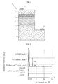
- FIG. 5 shows an example of conventional semiconductor light emitting device.
- the semiconductor light emitting device X shown in the figure includes an n-GaN layer 92 which is an n-type semiconductor layer formed on a substrate 91 , a p-GaN layer 93 which is a p-type semiconductor layer, and an active layer 94 having a multiple quantum well (hereinafter referred to as “MQW”) structure.
- the active layer 94 has a laminated structure made up of semiconductor layers containing InGaN with different In composition ratios.
- An n-side electrode 95 is formed on the lower surface (in FIG. 5 ) of the substrate 91
- a p-side electrode 96 is formed on an upper surface (in FIG.
- the active layer 94 is sandwiched between lower clad layers 97 a , 97 b and upper clad layers 98 a , 98 b .
- the lower clad layer 97 a and the upper clad layer 98 a are semiconductor layers containing InGaN and having the same In composition ratio as that of the barrier layer of the active layer 94 .
- the lower clad layers 97 a , 97 b and the upper clad layers 98 a , 98 b alleviate the lattice strain between the layers sandwiching the clad layers.
- Each of the layers constituting the semiconductor light emitting device X is very thin, having a thickness of several tens of nanometers.
- the In contained in the upper clad layer 98 a may be lost by sublimation due to difference between these layers in formation temperature or formation gas, for example.
- the In composition ratio in the upper clad layer 98 a unduly reduces, whereby the alleviation of the lattice strain between the active layer 94 and the p-GaN layer 93 is hindered.
- the present invention is proposed under the circumstances described above. It is, therefore, an object of the present invention to provide a semiconductor light emitting device which is capable of alleviating lattice strain between semiconductor layers and a method for manufacturing such a semiconductor light emitting device.
- a semiconductor light emitting device comprising a substrate, a first nitride semiconductor layer supported by the substrate, a second nitride semiconductor layer which is located farther from the substrate than the first nitride semiconductor layer is, an active layer formed between the first and the second nitride semiconductor layers and containing InGaN, a sublimation preventing layer formed between the active layer and the second nitride semiconductor layer and containing InGaN, and an In composition gradient layer sandwiched between the sublimation preventing layer and the second nitride semiconductor layer and having such In composition ratio gradient that the In composition ratio decreases in a thickness direction toward the second nitride semiconductor layer.
- the In composition ratio in the sublimation preventing layer is 0 to 1%.
- the sublimation preventing layer has a thickness of 3 to 20 nm.
- the In composition ratio gradient of the In composition gradient layer is so set that the In composition ratio decreases from 5% to 0% in the thickness direction from the sublimation preventing layer side toward the second nitride semiconductor layer side.
- a method for manufacturing a semiconductor light emitting device provided according to the first aspect of the present invention.
- the method comprises the step of forming the In composition gradient layer while monotonically increasing film formation temperature with time.
- the In composition gradient layer formation step is performed after the sublimation preventing layer is formed and before the second nitride semiconductor layer is formed.
- FIG. 1 is a sectional view showing an example of semiconductor light emitting device according to the present invention.
- FIG. 2 is a graph showing the In composition ratio in the thickness direction in Example 1.
- FIG. 3 is a graph showing the In composition ratio in the thickness direction in Example 2.
- FIG. 4 shows the change of film formation temperature in a manufacturing method of Example 1.
- FIG. 5 is a sectional view showing an example of conventional semiconductor light emitting device.
- FIG. 1 shows an example of semiconductor light emitting device according to the present invention.
- the semiconductor light emitting device A of this embodiment includes a substrate 1 , an n-GaN layer 2 , a superlattice layer 3 , an active layer 4 , a sublimation preventing layer 5 , an In composition gradient layer 6 , and a p-GaN layer 7 .
- the semiconductor light emitting device A is designed to emit blue light or green light.
- the substrate 1 may be made of e.g. sapphire and supports the n-GaN layer 2 , the superlattice layer 3 , the active layer 4 , the sublimation preventing layer 5 , the In composition gradient layer 6 , and the p-GaN layer 7 .
- the substrate 1 has a thickness of about 300 to 500 ⁇ m, for example.
- the n-GaN layer 2 is an n-type semiconductor layer formed by doping Si into GaN and an example of first nitride semiconductor layer of the present invention.
- the concept of the first nitride semiconductor layer of the present invention includes not only a layer directly formed on the substrate 1 like the n-GaN layer 2 but also a layer indirectly supported by the substrate 1 via a buffer layer made of e.g. AlN, GaN or AlGaN for alleviating lattice strain.
- the n-GaN layer 2 has a thickness of about 3 to 6 ⁇ m.
- the n-GaN layer 2 is formed with an n-side electrode 21 .
- the superlattice layer 3 has a superlattice structure in which InGaN layers and GaN layers are so laminated that the single atomic layers are alternately arranged.
- the superlattice layer 3 of this embodiment five to twenty InGaN layers having an In composition ratio of about 5 to 10% and five to twenty GaN layers are laminated.
- the thickness of the superlattice layer 3 is about 30 to 60 nm.
- the active layer 4 has an MQW structure containing InGaN and serves to amplify the light emitted by the recombination of electrons and holes.
- the active layer 4 is made up of a plurality of InGaN layers and a plurality of GaN layers which are alternately laminated.
- the In composition ratio in the InGaN layers is about 15%, so that the band gap of the InGaN layers is smaller than those of the n-GaN layer 2 and the superlattice layer 3 .
- the InGaN layers constitute well layers of the active layer 4 .
- the GaN layers constitute the barrier layers of the active layer 4 .
- In the active layer 4 of this embodiment three to seven InGaN layers and three to seven GaN layers are laminated.
- the thickness of the active layer 4 is about 50 to 150 nm.
- the sublimation preventing layer 5 contains InGaN and prevents the sublimation of In from the active layer 4 in the process of manufacturing the semiconductor light emitting device A.
- the sublimation preventing layer 5 has an In composition ratio of about 0 to 1% and a thickness of about 3 to 20 nm.
- the In composition gradient layer 6 contains InGaN.
- the In composition gradient layer 6 has different In composition ratios at different positions in the thickness direction. Specifically, in the In composition gradient layer, the In composition ratio reduces from the sublimation preventing layer 5 side toward the p-GaN layer 7 side. Preferably, the In composition ratio in the In composition gradient layer 6 is about 0 to 5%.
- the thickness of the In composition gradient layer 6 is about 3 to 16 nm.
- the p-GaN layer 7 is a p-type semiconductor layer formed by doping Mg into GaN and an example of second nitride semiconductor layer of the present invention.
- the p-GaN layer 7 has a thickness of about 100 to 1500 nm.
- the p-GaN layer 7 is formed with a p-side electrode 71 .
- FIG. 2 shows the In composition ratio in the sublimation preventing layer 5 and the In composition gradient layer 6 in Example 1 of the foregoing embodiment.
- the sublimation preventing layer 5 of this Example has an In composition ratio of 0.5% and a thickness of 3 nm.
- the In composition ratio in the In composition gradient layer 6 is 0.5% at the end adjoining the sublimation preventing layer 5 and 0% at the end adjoining the p-GaN layer 7 .
- the In composition ratio in the In composition gradient layer 6 linearly decreases monotonically in the thickness direction from the sublimation preventing layer 5 side toward the p-GaN layer 7 side.
- the thickness of the In composition gradient layer 6 is 9 nm.
- FIG. 2 shows In composition ratio in the sublimation preventing layer 5 and the In composition gradient layer 6 in Example 2 of the foregoing embodiment.
- the sublimation preventing layer 5 of this Example is the same as that of Example 1.
- the In composition ratio in the In composition gradient layer 6 is 5% at the end adjoining the sublimation preventing layer 5 and 0% at the end adjoining the p-GaN layer 7 .
- the In composition ratio in this Example is discontinuous at the boundary between the sublimation preventing layer 5 and the In composition gradient layer 6 .
- FIG. 4 shows the change of film formation temperature in a method for manufacturing a semiconductor light emitting device of Example 1.
- a substrate 1 is placed in a film formation chamber for MOCVD, and the film formation temperature, i.e., the temperature in the film formation chamber is set to 1,100° C.
- H 2 gas and N 2 gas are supplied into the film formation chamber to clean the substrate 1 .
- NH 3 gas, H 2 gas, N 2 gas and trimethylgallium (hereinafter referred to as “TMG”) gas are supplied into the film formation chamber.
- SiH 4 gas is supplied to perform doping of Si which is an n-type dopant.
- n-GaN layer 2 is formed on the substrate 1 .
- NH 3 gas, H 2 gas, N 2 gas, triethylgallium (hereinafter referred to as “TEG”) gas and trimethylindium (hereinafter referred to as “TMIn”) gas are supplied into the film formation chamber.
- TMG triethylgallium
- TMIn trimethylindium
- NH 3 gas, H 2 gas, N 2 gas and TMG gas are supplied into the film formation chamber, whereby a GaN layer is formed.
- a superlattice layer 3 having a thickness of about 30 to 60 nm is formed.
- NH 3 gas, H 2 gas, N 2 gas, TEG gas and TMIn gas are supplied into the film formation chamber. It is to be noted that the proportion of the TMIn gas is adjusted depending on the In composition ratio in the InGaN layer to be formed. By this process, an InGaN layer as a well layer having an In composition ratio of about 15% is formed.
- an InGaN layer as a well layer and the formation of a GaN layer as a barrier layer are alternately performed.
- an active layer 4 having an MQW structure is obtained.
- NH 3 gas, H 2 gas, N 2 gas, TEG gas and TMIn gas are supplied into the film formation chamber.
- a sublimation preventing layer 5 having an In composition ratio of about 0.5% is formed on the active layer 4 .
- the sublimation preventing layer 5 is formed to have a thickness of 3 nm.
- the In composition gradient layer 6 in which the In composition ratio decreases from 0.5% to 0% in the thickness direction is formed.
- the In composition gradient layer 6 is formed to have a thickness of 9 nm.
- NH 3 gas, H 2 gas, N 2 gas and TMG gas are supplied.
- Cp 2 Mg gas is supplied to perform doping of Mg which is a p-type dopant.
- a p-GaN layer 7 is formed.
- an n-side electrode 21 and a p-side electrode 71 are formed, whereby the semiconductor light emitting device A is completed.
- the In composition gradient layer 6 and the p-GaN layer 7 are formed, with the active layer 4 covered with the sublimation preventing layer 5 .
- the active layer 4 is not exposed to high temperature over 1,000° C., so that the sublimation of In from the active layer 4 is reliably prevented.
- the active layer 4 has a proper composition, so that the amount of light to be emitted from the semiconductor light emitting device A increases.
- the sublimation of In is effectively prevented particularly when the In composition ratio in the sublimation preventing layer 5 is 0.5% as is in Example 1.
- the In composition ratio in the sublimation preventing layer 5 is 0 to 1%, both of the In sublimation from the active layer 4 and the increase of lattice strain are prevented.
- the thickness of the sublimation preventing layer 5 is not smaller than 3 nm, segregation due to the small thickness of the sublimation preventing layer 5 is prevented. Moreover, when the thickness of the sublimation preventing layer 5 is not larger than 20 nm, hole injection from the p-GaN layer 7 to the active layer 4 is prevented from becoming insufficient.
- Example 1 the active layer 4 and the sublimation preventing layer 5 are bonded to the p-GaN layer 7 via the In composition gradient layer 6 so that the change in In composition ratio is continuous. As a result, considerable lattice strain between the active layer 4 and the p-GaN layer 7 is properly prevented. As a result, the laminated structure of the semiconductor light emitting device A is reliably prevented from breaking. In the present invention, however, the In composition ratio of the sublimation preventing layer 5 and that of the In composition gradient layer 6 may not be continuous at the boundary. Even in such a case, by providing the In composition gradient layer 6 with proper gradient of In composition ratio like that of Example 2, considerable lattice strain is prevented.
- the superlattice layer 3 may be so designed that the electrical resistance in a direction perpendicular to the thickness direction is smaller than the electrical resistance in the thickness direction. This arrangement ensures that the current flows uniformly through the entire surface of the superlattice layer 3 and prevents the current from flowing locally through a particular portion. As a result, the amount of current, and hence, the amount of light emitted from the semiconductor light emitting device A increases.
- a higher film formation temperature provides a lower In composition ratio.
- an In composition gradient layer 6 whose In composition ratio monotonically decreases in the thickness direction is obtained. Since the film formation temperature and the In composition ratio closely correspond to each other, the In composition ratio in the In composition gradient layer 6 is accurately controlled, which is advantageous for alleviating the lattice strain between the active layer 4 and the p-GaN layer 7 .
- the semiconductor light emitting device and its manufacturing method are not limited to the foregoing embodiments.
- the specific structure of each part of the semiconductor light emitting device and the manufacturing method may be varied in many ways.
- the gradient of the In composition ratio in the In composition gradient layer 6 does not necessarily be linear but may be like a quadratic curve or a curve of a higher order, for example.
- an active layer made up of two kinds of InGaN layers which differ from each other in In composition ratio may be employed.
- the active layer of the present invention is not limited to one having an MQW structure.
- the semiconductor light emitting device A of the present invention may be designed to emit light of various wavelengths. For instance, in addition to blue light and green light, the semiconductor light emitting device may be designed to emit white light.
Landscapes
- Engineering & Computer Science (AREA)
- Manufacturing & Machinery (AREA)
- Computer Hardware Design (AREA)
- Microelectronics & Electronic Packaging (AREA)
- Power Engineering (AREA)
- Physics & Mathematics (AREA)
- Condensed Matter Physics & Semiconductors (AREA)
- General Physics & Mathematics (AREA)
- Led Devices (AREA)
Applications Claiming Priority (3)
| Application Number | Priority Date | Filing Date | Title |
|---|---|---|---|
| JP2006030963A JP2007214257A (ja) | 2006-02-08 | 2006-02-08 | 半導体発光素子およびその製造方法 |
| JP2006-030963 | 2006-02-08 | ||
| PCT/JP2007/052220 WO2007091637A1 (ja) | 2006-02-08 | 2007-02-08 | 半導体発光素子およびその製造方法 |
Publications (2)
| Publication Number | Publication Date |
|---|---|
| US20090272992A1 US20090272992A1 (en) | 2009-11-05 |
| US8222655B2 true US8222655B2 (en) | 2012-07-17 |
Family
ID=38345231
Family Applications (1)
| Application Number | Title | Priority Date | Filing Date |
|---|---|---|---|
| US12/223,739 Expired - Fee Related US8222655B2 (en) | 2006-02-08 | 2007-02-08 | Semiconductor light-emitting device and process for producing the same |
Country Status (3)
| Country | Link |
|---|---|
| US (1) | US8222655B2 (ja) |
| JP (1) | JP2007214257A (ja) |
| WO (1) | WO2007091637A1 (ja) |
Families Citing this family (6)
| Publication number | Priority date | Publication date | Assignee | Title |
|---|---|---|---|---|
| JP2008235606A (ja) * | 2007-03-20 | 2008-10-02 | Sony Corp | 半導体発光素子、半導体発光素子の製造方法、バックライト、表示装置、電子機器および発光装置 |
| JP2010263189A (ja) * | 2009-04-07 | 2010-11-18 | Sharp Corp | 窒化物半導体発光ダイオード |
| JP2011060900A (ja) * | 2009-09-08 | 2011-03-24 | Showa Denko Kk | 半導体発光素子の製造方法およびランプ、電子機器、機械装置 |
| JP5417307B2 (ja) | 2010-12-02 | 2014-02-12 | 株式会社東芝 | 半導体発光素子 |
| GB2487531A (en) * | 2011-01-20 | 2012-08-01 | Sharp Kk | Substrate system consisting of a metamorphic transition region comprising a laminate of AlxGa1-x N and the same material as the substrate. |
| WO2019106843A1 (ja) * | 2017-12-01 | 2019-06-06 | 三菱電機株式会社 | 半導体装置の製造方法、半導体装置 |
Citations (9)
| Publication number | Priority date | Publication date | Assignee | Title |
|---|---|---|---|---|
| JPH1154794A (ja) | 1997-07-29 | 1999-02-26 | Toshiba Corp | 化合物半導体素子及びその製造方法 |
| JPH11340580A (ja) | 1997-07-30 | 1999-12-10 | Fujitsu Ltd | 半導体レーザ、半導体発光素子、及び、その製造方法 |
| JP2001326426A (ja) | 2000-05-17 | 2001-11-22 | Sharp Corp | Iii−v族化合物半導体発光素子及びその製造方法、並びに情報記録再生装置 |
| JP2002261395A (ja) | 2000-12-28 | 2002-09-13 | Sony Corp | 半導体発光素子およびその製造方法ならびに半導体装置およびその製造方法 |
| US20020195606A1 (en) * | 2001-01-16 | 2002-12-26 | Edmond John Adam | Group III nitride LED with undoped cladding layer and multiple quantum well |
| US20030006409A1 (en) | 2001-07-06 | 2003-01-09 | Kabushiki Kaisha Toshiba | Nitride compound semiconductor element |
| JP2003081697A (ja) | 2001-09-10 | 2003-03-19 | Sony Corp | 窒化物系iii−v族化合物半導体基板およびその製造方法ならびに半導体発光素子の製造方法ならびに半導体装置の製造方法 |
| US6555403B1 (en) | 1997-07-30 | 2003-04-29 | Fujitsu Limited | Semiconductor laser, semiconductor light emitting device, and methods of manufacturing the same |
| JP2005150627A (ja) | 2003-11-19 | 2005-06-09 | Sumitomo Electric Ind Ltd | 発光ダイオード及びその製造方法 |
Family Cites Families (1)
| Publication number | Priority date | Publication date | Assignee | Title |
|---|---|---|---|---|
| JP4747254B2 (ja) * | 2001-09-13 | 2011-08-17 | Jnc株式会社 | 液晶性化合物、液晶組成物および液晶表示素子 |
-
2006
- 2006-02-08 JP JP2006030963A patent/JP2007214257A/ja active Pending
-
2007
- 2007-02-08 WO PCT/JP2007/052220 patent/WO2007091637A1/ja active Application Filing
- 2007-02-08 US US12/223,739 patent/US8222655B2/en not_active Expired - Fee Related
Patent Citations (12)
| Publication number | Priority date | Publication date | Assignee | Title |
|---|---|---|---|---|
| JPH1154794A (ja) | 1997-07-29 | 1999-02-26 | Toshiba Corp | 化合物半導体素子及びその製造方法 |
| US6309459B1 (en) * | 1997-07-29 | 2001-10-30 | Kabushiki Kaisha Toshiba | Compound semiconductor element and its manufacturing method |
| JPH11340580A (ja) | 1997-07-30 | 1999-12-10 | Fujitsu Ltd | 半導体レーザ、半導体発光素子、及び、その製造方法 |
| US6555403B1 (en) | 1997-07-30 | 2003-04-29 | Fujitsu Limited | Semiconductor laser, semiconductor light emitting device, and methods of manufacturing the same |
| JP2001326426A (ja) | 2000-05-17 | 2001-11-22 | Sharp Corp | Iii−v族化合物半導体発光素子及びその製造方法、並びに情報記録再生装置 |
| JP2002261395A (ja) | 2000-12-28 | 2002-09-13 | Sony Corp | 半導体発光素子およびその製造方法ならびに半導体装置およびその製造方法 |
| US7339195B2 (en) | 2000-12-28 | 2008-03-04 | Sony Corporation | Semiconductor light emitting device, its manufacturing method, semiconductor device and its manufacturing method |
| US20020195606A1 (en) * | 2001-01-16 | 2002-12-26 | Edmond John Adam | Group III nitride LED with undoped cladding layer and multiple quantum well |
| US20030006409A1 (en) | 2001-07-06 | 2003-01-09 | Kabushiki Kaisha Toshiba | Nitride compound semiconductor element |
| JP2003023220A (ja) | 2001-07-06 | 2003-01-24 | Toshiba Corp | 窒化物半導体素子 |
| JP2003081697A (ja) | 2001-09-10 | 2003-03-19 | Sony Corp | 窒化物系iii−v族化合物半導体基板およびその製造方法ならびに半導体発光素子の製造方法ならびに半導体装置の製造方法 |
| JP2005150627A (ja) | 2003-11-19 | 2005-06-09 | Sumitomo Electric Ind Ltd | 発光ダイオード及びその製造方法 |
Also Published As
| Publication number | Publication date |
|---|---|
| JP2007214257A (ja) | 2007-08-23 |
| US20090272992A1 (en) | 2009-11-05 |
| WO2007091637A1 (ja) | 2007-08-16 |
Similar Documents
| Publication | Publication Date | Title |
|---|---|---|
| JP4954536B2 (ja) | 窒化物半導体発光素子 | |
| US7884350B2 (en) | Semiconductor light emitting device and method for manufacturing the same | |
| KR100752007B1 (ko) | 3족 질화물계 화합물 반도체 발광 소자 및 그 제조 방법 | |
| US20100133506A1 (en) | Nitride semiconductor light emitting element and method for manufacturing nitride semiconductor | |
| KR100784065B1 (ko) | 질화물 반도체 발광소자 및 그 제조방법 | |
| WO2014178248A1 (ja) | 窒化物半導体発光素子 | |
| EP3360168B1 (en) | Iii-nitride semiconductor light emitting device having amber-to-red light emission (>600 nm) and a method for making same | |
| US7953134B2 (en) | Semiconductor light-emitting device | |
| US9099572B2 (en) | Semiconductor light emitting element and method of manufacturing semiconductor light emitting element | |
| US8222655B2 (en) | Semiconductor light-emitting device and process for producing the same | |
| TW201937753A (zh) | 氮化物半導體發光元件 | |
| JP2008103665A (ja) | 窒化物半導体デバイス及びその製造方法 | |
| WO2006057485A1 (en) | Iii-nitride semiconductor light emitting device | |
| KR101666836B1 (ko) | 형광체 없는 백색 발광다이오드 성장 기술 | |
| JP4884826B2 (ja) | 半導体発光素子 | |
| KR101692181B1 (ko) | 질화물 반도체 발광소자 및 그 제조 방법 | |
| WO2016002684A1 (ja) | Led素子 | |
| US8633469B2 (en) | Group III nitride semiconductor light-emitting device | |
| JP2009224370A (ja) | 窒化物半導体デバイス | |
| KR100728132B1 (ko) | 전류 확산층을 이용한 발광 다이오드 | |
| JP6192722B2 (ja) | オプトエレクトロニクス半導体ボディ及びオプトエレクトロニクス半導体チップ | |
| KR20130015112A (ko) | 발광 다이오드 및 그것을 제조하는 방법 | |
| JP2008227103A (ja) | GaN系半導体発光素子 | |
| KR101373804B1 (ko) | 백색 발광다이오드 및 그 제조방법 | |
| US20230395750A1 (en) | Light emitting element |
Legal Events
| Date | Code | Title | Description |
|---|---|---|---|
| AS | Assignment |
Owner name: ROHM CO., LTD., JAPAN Free format text: ASSIGNMENT OF ASSIGNORS INTEREST;ASSIGNORS:TSUTSUMI, KAZUAKI;ITO, NORIKAZU;SONOBE, MASAYUKI;AND OTHERS;REEL/FRAME:021687/0506 Effective date: 20081003 |
|
| STCF | Information on status: patent grant |
Free format text: PATENTED CASE |
|
| FEPP | Fee payment procedure |
Free format text: PAYOR NUMBER ASSIGNED (ORIGINAL EVENT CODE: ASPN); ENTITY STATUS OF PATENT OWNER: LARGE ENTITY |
|
| FPAY | Fee payment |
Year of fee payment: 4 |
|
| FEPP | Fee payment procedure |
Free format text: MAINTENANCE FEE REMINDER MAILED (ORIGINAL EVENT CODE: REM.); ENTITY STATUS OF PATENT OWNER: LARGE ENTITY |
|
| LAPS | Lapse for failure to pay maintenance fees |
Free format text: PATENT EXPIRED FOR FAILURE TO PAY MAINTENANCE FEES (ORIGINAL EVENT CODE: EXP.); ENTITY STATUS OF PATENT OWNER: LARGE ENTITY |
|
| STCH | Information on status: patent discontinuation |
Free format text: PATENT EXPIRED DUE TO NONPAYMENT OF MAINTENANCE FEES UNDER 37 CFR 1.362 |
|
| FP | Lapsed due to failure to pay maintenance fee |
Effective date: 20200717 |