US8129687B2 - Lighting system, method of lighting, optical detector, and method of optical detection - Google Patents
Lighting system, method of lighting, optical detector, and method of optical detection Download PDFInfo
- Publication number
- US8129687B2 US8129687B2 US12/308,619 US30861907A US8129687B2 US 8129687 B2 US8129687 B2 US 8129687B2 US 30861907 A US30861907 A US 30861907A US 8129687 B2 US8129687 B2 US 8129687B2
- Authority
- US
- United States
- Prior art keywords
- light
- electron
- optical
- electron beam
- negative refraction
- Prior art date
- Legal status (The legal status is an assumption and is not a legal conclusion. Google has not performed a legal analysis and makes no representation as to the accuracy of the status listed.)
- Expired - Fee Related, expires
Links
Images




Classifications
-
- H—ELECTRICITY
- H01—ELECTRIC ELEMENTS
- H01J—ELECTRIC DISCHARGE TUBES OR DISCHARGE LAMPS
- H01J63/00—Cathode-ray or electron-stream lamps
- H01J63/06—Lamps with luminescent screen excited by the ray or stream
-
- B—PERFORMING OPERATIONS; TRANSPORTING
- B82—NANOTECHNOLOGY
- B82Y—SPECIFIC USES OR APPLICATIONS OF NANOSTRUCTURES; MEASUREMENT OR ANALYSIS OF NANOSTRUCTURES; MANUFACTURE OR TREATMENT OF NANOSTRUCTURES
- B82Y15/00—Nanotechnology for interacting, sensing or actuating, e.g. quantum dots as markers in protein assays or molecular motors
-
- B—PERFORMING OPERATIONS; TRANSPORTING
- B82—NANOTECHNOLOGY
- B82Y—SPECIFIC USES OR APPLICATIONS OF NANOSTRUCTURES; MEASUREMENT OR ANALYSIS OF NANOSTRUCTURES; MANUFACTURE OR TREATMENT OF NANOSTRUCTURES
- B82Y20/00—Nanooptics, e.g. quantum optics or photonic crystals
-
- G—PHYSICS
- G02—OPTICS
- G02B—OPTICAL ELEMENTS, SYSTEMS OR APPARATUS
- G02B1/00—Optical elements characterised by the material of which they are made; Optical coatings for optical elements
- G02B1/002—Optical elements characterised by the material of which they are made; Optical coatings for optical elements made of materials engineered to provide properties not available in nature, e.g. metamaterials
- G02B1/007—Optical elements characterised by the material of which they are made; Optical coatings for optical elements made of materials engineered to provide properties not available in nature, e.g. metamaterials made of negative effective refractive index materials
Definitions
- the present invention relates to a lighting system, a method of lighting, an optical detector, and a method of optical detection which can be used in an optical image detector such as a microscope, a camera, and an endoscope, an optical information writing and reading apparatus such as a pickup for an optical disc, and a lithographic apparatus such as a stepper.
- an optical image detector such as a microscope, a camera, and an endoscope
- an optical information writing and reading apparatus such as a pickup for an optical disc
- a lithographic apparatus such as a stepper.
- a material which shows a negative refraction response for the specific electromagnetic waves will be called as a ‘material exhibiting negative refraction’. It is needless to mention that, an expression ‘a material exhibiting negative refraction’ is a concept of a wider sense than the negative refraction material.
- materials such as metallic films, chiral substances, photonic crystals, meta-materials, left-handed materials, backward wave materials, and negative phase velocity media have been known.
- FIG. 17 shows refraction of light in an ordinary optical material (hereinafter called as ‘an ordinary optical material’) having a positive refractive index.
- ⁇ i denotes an angle of incidence
- ⁇ r denotes an angle of emergence
- n 1 denotes a refracting index of the medium 1
- n 2 denotes a refractive index of the medium 2 .
- FIG. 18 shows a refraction of light when the refractive index n 2 of the medium 2 takes a negative value.
- the light which is incident is refracted in a direction opposite to a direction of refraction shown in FIG. 17 with respect to a normal of the boundary surface.
- the angle of refraction ⁇ r is let to be a negative value, the abovementioned Snell's law is satisfied.
- FIG. 19 shows an imaging relationship by a convex lens 13 in which an ordinary optical material is used.
- Light from an object point 11 A on an object plane 11 is converged to an image point 12 A on an image plane 12 by the convex lens 13 .
- the refractive index of the lens is positive, for imaging (converging), a lens surface is required to have a finite curvature.
- FIG. 20 shows an imaging relationship by a negative refraction lens 14 .
- Light from an object point 11 B on an object plane 11 is converged to an image point 12 B on an image plane 12 by the negative refraction lens 14 .
- non-patent literature 11 a method for realizing a non-uniform imaging by forming a curved surface lens by a material exhibiting negative refraction has been disclosed.
- a condition for the perfect imaging being extremely strict, and since a material having a predetermined refractive index gradient in addition to exhibiting negative refraction is necessary, it is not realistic.
- all the negative refraction lenses realized in the world have almost a uniform refractive index spatially, and a surface thereof through which light (electromagnetic waves) passes is a plane surface. Therefore, a spatially uniform flat plate made of a material exhibiting negative refraction will here onward be called appropriately as a ‘negative refraction lens’.
- spatially uniform means that, it is uniform with a scale which is larger than a wavelength of the electromagnetic waves. Consequently, it means that, in a case of realizing the negative refraction by an artificial structural material such as photonic crystal and a meta-material, an effective refractive index (or an effective permittivity or an effective magnetic permeability) which is attributable to the structure is spatially uniform.
- a theoretical upper limit value of resolution is determined by a diffraction limit.
- the minimum distance between two resolvable points is about ⁇ /NA.
- ⁇ is a wavelength used
- NA is a numerical aperture.
- a structure smaller than the diffraction limit cannot carry out image dissection by an optical system.
- Light which has been emitted from the object point 11 A on the object plane 11 is formed of two light waves namely, radiation light which reaches a far distance, and evanescent waves which are attenuated at a distance of about wavelength from the object point 11 A.
- the radiation light corresponds to a low-frequency component of information on the image plane 11 .
- the evanescent waves correspond to a high-frequency component of the information on the image plane 11 .
- a boundary of the radiation light and the evanescent waves has a spatial frequency equivalent to 1/ ⁇ .
- the evanescent waves have frequency within the object plane larger than 1/ ⁇ . Therefore, the evanescent waves have a wave number component in a direction of propagation of light waves perpendicular to the evanescent waves becoming an imaginary number. Therefore, there is a rapid attenuation with receding from the object plane 11 .
- All the components of the radiation light on the other hand do not advance to the optical system.
- a part of the radiation light is vignetted by an aperture in the optical system. Therefore, only a component smaller than NA/ ⁇ of the spatial frequency on the object plane 11 reaches the image plane 12 .
- NA/ ⁇ of the spatial frequency on the object plane 11 reaches the image plane 12 .
- the high-frequency component from the information held by the object point 11 A is missing. Accordingly, this becomes a spreading of a point image by diffraction, and restricts the resolution.
- a method of manufacturing a negative refraction material by using photonic crystal has been disclosed.
- the photonic crystal in which an air rod is disposed in a hexagonal lattice form in a dielectric substance, there exists a photonic band in which, the effective refractive index is isotropic as well as negative.
- the photonic crystal can be deemed as a two-dimension uniform negative refraction material with respect to electromagnetic waves of a frequency band suitable for a photonic band.
- non-patent literature 6 There has been a theoretical counterargument as described in non-patent literature 6 for example, to the perfect imaging by the negative refraction lens, which lead to a controversy. However, in recent years, a theory of the negative refraction lens disclosed in non-patent literature 3 has been generally accepted.
- an optical system in which, an ordinary optical material is used, it is possible to create an aplanatic point, in other words, a point at which, a spherical aberration and coma aberration become zero simultaneously.
- An image by this optical system always becomes a virtual image.
- a negative refraction material when used, it is possible to form a real image by arranging an object plane at the aplanatic point (refer to non-patent literature 7 for example). In this manner, by using a negative refraction material, unique optical designing which was not available so far becomes possible.
- non-patent literature 9 silver exhibits a negative permittivity for light of a wavelength in a range of 330 nm to 900 nm. Furthermore, according to non-patent literature 10, even in a chiral substance having a helical structure, there exists a photonic band exhibiting negative refraction.
- Phenomenon of negative refraction has unique characteristics which are different from an ordinary optical material, such as having a negative angle of refraction, having a phase velocity and a group velocity in opposite direction, and an electric field, a magnetic field, and a wave number vector forming a left-handed system in this order.
- a material exhibiting negative refraction is also called as a negative phase velocity material, a left-handed material, a backward-wave material, and a negative refraction material.
- a material exhibiting negative refraction is also called as a negative phase velocity material, a left-handed material, a backward-wave material, and a negative refraction material.
- it will be treated as a type of such material exhibiting negative refraction. Such treatment is does not contradict at all to a definition of the abovementioned material exhibiting negative refraction.
- a meta-material which is made of a metal resonator array is sometimes also called as a left-handed substance or a left-handed metamaterial. Such materials are also to be included in materials exhibiting negative refraction.
- Non-patent literature 1 V. G. Veselago et al., Sov. Phys. Usp. 10, 509 (1968)
- the negative refraction lens forms an image in which, the high-frequency component is retained by transmitting the evanescent waves.
- a negative refraction lens for generating arbitrarily some sort of optical image having the high-frequency component by using a negative refraction lens, or for detecting the high-frequency component from an optical image generated from an object etc. by a negative refraction lens, there are following issues related to a method of lighting and a method of detection.
- a detector for detecting information of a certain desired high-frequency component, it is necessary that a detector is placed directly on a same magnified-image plane by the negative refraction lens, and that the detector has a detection band spatial resolution larger than the desired high-frequency component.
- a two-point resolution of a microscope having an ordinary water-immersion objective lens is approximately 0.3 ⁇ m.
- the wavelength is let to be 0.5 ⁇ m, the numerical aperture is let to be 0.75, and refractive index of water is let to be 1.333.
- a pixel interval (pixel dimension) has to be not more than half of 0.03 ⁇ m, in other words, not more than 0.015 ⁇ m.
- a size of the detector and the light source has to be not more than 0.015 ⁇ m similarly as in a case of the image sensor described above.
- an SNOM Sccanning Near field Optical Microscope
- a diameter is approximately 0.05 ⁇ m to 0.1 ⁇ m. This is three times larger than the condition shown in the abovementioned example, in other words, three times larger than the diameter of 0.015 ⁇ m or less of the detector and the light source.
- the present invention is made in view of the abovementioned issues, and an object of the present invention is to provide a lighting system, method of lighting, optical detector, and method of optical detection having a high spatial resolution appropriate for a high-frequency component by the evanescent waves in a negative refraction lens
- a lighting system including
- a light emitter which includes a luminescent material which emits light when an energy is applied thereon,
- an optical system which includes an optical element which is formed of a material exhibiting negative refraction, and which is for projecting the light emitted from the light emitter, on an object.
- the light emitter is in a form of a thin film.
- an electron beam is used as the energy to be applied to the light emitter.
- an electrode made of an electroconductive material and having as shape of a protrusion is used as the probe.
- a method of lighting including
- an optical detector including
- an optical detecting body which is made of a photoconductive material
- an optical system which includes an optical element formed of a material exhibiting negative refraction, and which projects on the optical detecting body, object light which is emitted from the object, and
- a probe for applying an energy to an area smaller than a diffraction limit of the object light, of the optical detecting body is a probe for applying an energy to an area smaller than a diffraction limit of the object light, of the optical detecting body.
- the optical detecting body is in a form of a thin film.
- an electron beam is used as the energy to be applied to the light emitter.
- an electrode made of an electroconductive material, and having a shape of a protrusion is used as the probe.
- a method of optical detection including
- FIG. 1 is a diagram showing a schematic structure of an electron beam excitation light source according to a first embodiment of the present invention
- FIG. 2 is a diagram showing a schematic structure of a light emitter thin film with an electroconductive layer in the first embodiment
- FIG. 3 is a diagram showing a schematic structure of an optical image observation unit for an electron microscope in the first embodiment
- FIG. 4 is a diagram showing a schematic structure of the electron beam excitation light source in which, a light emitter thin film is formed to be a negative refraction lens used combinedly as an optical window in the first embodiment;
- FIG. 5 is a diagram showing a schematic structure of an electron beam excitation light source by an ultracompact electron gun, according to a second embodiment of the present invention.
- FIG. 6 is a diagram showing a perspective structure of the ultracompact electron gun in the second embodiment
- FIG. 7 is a diagram showing a cross-sectional structure of the ultracompact electron gun in the second embodiment
- FIG. 8 is a diagram showing a cross-sectional structure of the ultracompact electron gun with a deflector in the second embodiment
- FIG. 9 is a diagram showing a schematic structure of the deflector in the second embodiment.
- FIG. 10 is a diagram showing a schematic structure of a light source by a needle-shaped electrode according to a third embodiment of the present invention.
- FIG. 11 is a diagram showing a schematic structure of a light emitter thin film in the third embodiment.
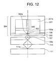
- FIG. 12 is a diagram showing a schematic structure of a light source by a needle-shaped electrode with an actuator in the third embodiment
- FIG. 13 is a perspective view showing a schematic structure of a surrounding of the needle-shaped electrode in the third embodiment
- FIG. 14 is a diagram explaining an equivalent circuit of an image pickup tube
- FIG. 15 is a diagram showing an image pickup tube detector according to a fourth embodiment of the present invention.
- FIG. 16 is a diagram showing a cross-sectional structure of an optical window and a target in the fourth embodiment
- FIG. 17 is a diagram showing refraction of light in an ordinary optical material
- FIG. 18 is a diagram showing refraction of light in a material having a negative refractive index
- FIG. 19 is a diagram showing an imaging relationship by a convex lens in which, an ordinary optical material is used.
- FIG. 20 is a diagram showing an imaging relationship by a negative refraction lens.
- FIG. 1 shows a schematic structure of an electron beam excitation light source 100 according to the first embodiment of the present invention.
- a cathode 101 which discharges electrons, supplies an electron beam 102 which is made of electrons discharged.
- An anode (an accelerating electrode) 103 applies an acceleration voltage to the electrons discharged.
- An electron lens 104 converges the electron beam.
- the cathode 101 , the anode (accelerating electrode) 103 , and the electron lens 104 correspond to a probe, and the electron beam 102 corresponds to an energy.
- a deflector 105 deflects the electron beam in a direction orthogonal to a central axis 119 .
- the light emitter thin film 106 is formed of a light emitting material.
- An optical window 107 is formed of an optically transparent material.
- a vacuum chamber 108 is formed to maintain low, an air pressure in a path of the electron beam. The vacuum chamber 108 accommodates the cathode 101 , the anode (accelerating electrode) 103 , and the deflector 105 .
- Light 109 emitted by the light emitter thin film 106 is incident on a negative refraction lens 110 which is made of a negative refraction material.
- light emerged from the negative refraction lens 110 is irradiated on an object 111 .
- the electrode beam 102 made of electrons discharged from the cathode 101 is accelerated by an electric field formed by the anode 103 .
- a de Broglie wavelength ⁇ (nm) of the electron beam accelerated at voltage E (V) is obtained by the following expression (2).
- h Planck's constant (6.624 ⁇ 10 ⁇ 34 J ⁇ s)
- m is a mass of electrons (9.107 ⁇ 10 ⁇ 31 kg)
- e is an electric charge of electrons (1.602 ⁇ 10 ⁇ 19 C).
- the accelerated electron beam 102 is converged at the electron lens 104 .
- the electron beam 102 is irradiated on the light emitter thin film 106 as a converged electron beam 102 a . It is possible to narrow down easily a diameter of the electron beam at this time to about 1 nm by increasing an acceleration voltage sufficiently, and adjusting a focal point by the electron lens 104 . Furthermore, by using a lens in which a spherical aberration is corrected favorably, as the electron lens 104 , it is also possible to narrow down the diameter of the electron beam to about 0.1 nm.
- An area of the light emitter thin film 106 irradiated by the electron beam 102 a is excited by electrons which are irradiated. Accordingly, this area becomes a spot light source area 106 a and emits light 109 a .
- the light 109 a is transmitted through the optical window 107 , and is incident on the negative refraction lens 110 . Further, by a perfect imaging effect of the negative refraction lens 110 , the spot light source area 106 a is projected on the object 111 . As a result of this, an image of the spot light source area 106 a is formed as a spot illuminated area 111 a on the object 111 .
- spot light having a diameter same as a diameter of the converged electron beam 102 a is formed on the object 111 . Consequently, according to this embodiment, it is possible to light the object 111 by the spot light of a diameter same as in a case of lighting by an electron beam, in other words, a diameter in a range of 1 nm to 0.1 nm which was not possible so far.
- the deflector 105 it is possible to deflect the converged electron beam 102 a in a direction orthogonal to the central axis 119 by the deflector 105 .
- the converged electron beam 102 a is deflected to a left side in the diagram, it becomes a deflected converged beam 102 b .
- the spot light source area 106 a of the light emitter thin film 106 moves to a spot light source area 106 b.
- the light 109 a moves to light 109 b .
- the spot illuminated area 111 a on the object 111 moves to a spot illuminated area 111 b .
- the object 111 by applying to the object 111 an object which needs irradiation of minute and high resolution, application in various fields are possible.
- a heat sensitive material or a photosensitive material it is possible to let to be an exposing unit for lithography which manufactures minute structures such as a semiconductor and a micro machine.
- a writing unit for an optical information equipment such as an optical disc.
- a structure may be let to be such that it detects an object light such as a reflected light, transmitted light, scattered light, and fluorescence emitted from the object 111 by irradiating the light 109 , and when an optical information equipment medium such as an optical disc is used as the object 111 , it is possible to let it to be a reading apparatus for the optical information equipment. Furthermore, when an object for observation of an optical image is used as the object 111 , it becomes an optical image observation apparatus such as a camera and a microscope.
- the object 111 it is not necessary to place the object 111 in vacuum, and further, it may be handled upon placing in any environment and medium provided that it is a substance which allows the light to be transmitted irrespective of whether it is a gas, a liquid, or a solid. Consequently, there are extremely few constraints on use. Furthermore, whereas, the electron beam does not affect except a surface of the object 111 , when the object 111 is transparent, the light 109 can affect up to an inside of the object.
- the cathode 101 a form and a structure are immaterial provided that it has an effect of discharging electrons in a space, such as a thermionic emission type in which, electrons are discharged by heating an electrode, and a field emission type in which electrons are discharged from an electrode by a high electric field.
- a thermionic emission type in which, electrons are discharged by heating an electrode
- a field emission type in which electrons are discharged from an electrode by a high electric field.
- an electron lens an electromagnetic lens which carries out converging of electron beams by a magnetic field, or an electrostatic lens which carries out converging of electron beams by an electrostatic field may be used.
- the deflector 105 may also similarly be of an electromagnetic type or an electrostatic type.
- any material provided that it is a substance which emits light by irradiation of electron beam may be used.
- it may be a material which is excited to a high-energy state by irradiation of electron beam, and which exhibits cathodoluminescence in which light is emitted during a process of returning to a low-energy state, or may be a substance which exhibits bremsstrahlung in which, the electrons directly emit light during a process of deceleration of an irradiated electron beam in that medium.
- the fluorescent substance As a substance exhibiting cathode luminescence, fluorescent substances and phosphorescent substances are available, and both these substances can be used. More preferably, due to a reason of even shorter afterglow time, the fluorescent substance is appropriate than the phosphorescent substance. This is because, when the afterglow time is long, with a deflection scanning of the electron beam, an area of the spot light source area 106 a becomes large substantially, and this leads to a decrease in the spatial resolution.
- fluorescent substance As a fluorescent substance, the following can be used preferably.
- a phosphorescent substance the following can be used preferably.
- an optical transition radiation in which, electrons at the time of being incident on a medium having a different permittivity are irradiated from a boundary surface of medium, is available.
- a substance which causes optical transition radiation a metal or a dielectric substance may be used.
- a metal such as silver, aluminum, or stainless steel can be used.
- a merit of using optical transition radiation light as the light source is that the afterglow time is extremely short.
- the short afterglow time is desirable.
- the afterglow time for the optical transition radiation light is ps, or in other words, about 10 ⁇ 12 sec, thereby making it possible to make much shorter.
- FIG. 2 shows a schematic structure of a light emitter thin film 114 with an electroconductive layer (hereinafter, ‘electroconductive layer light emitter thin film 114 ’) which is a preferable form in a case of using a substance exhibiting cathodoluminescence as the light emitter thin film 106 in particular, in the first embodiment.
- electroconductive layer light emitter thin film 114 an electroconductive layer which is a preferable form in a case of using a substance exhibiting cathodoluminescence as the light emitter thin film 106 in particular, in the first embodiment.
- an electroconductive layer 112 has a function of removing electrons which have charged the light emitter thin film 106 .
- a transparent electroconductive layer 113 removes electrons which have transmitted through the light emitter thin film 106 , as well as allows the light 109 emitted from the light emitter thin film 106 to be transmitted through. It is desirable that the electroconductive layer 112 and the transparent electroconductive layer 113 are kept at an electric potential same as of the anode 103 and the vacuum chamber 108 respectively in FIG. 1 .
- the electroconductive layer light emitter thin film 114 When the electroconductive layer light emitter thin film 114 is used, it is possible to let the electric potential in the vacuum chamber 108 to be almost constant. Therefore, there is an effect that it is possible to reduce shifting of an irradiated position due to a path of the electron beam 102 being disturbed by an unnecessary electric field. Furthermore, even when a surface of the light emitter thin film 106 is charged supposedly, the electrons are removed rapidly via the electroconductive layer 112 .
- the electroconductive layer 112 it is required to have an electroconductive property, and a property that makes an electron beam be irradiated from an upper side in the diagram to reach the light emitter thin film 106 at a lower side thereof without being blocked.
- an electroconductive property and a property that makes an electron beam be irradiated from an upper side in the diagram to reach the light emitter thin film 106 at a lower side thereof without being blocked.
- the transparent electroconductive layer 113 it is required to have an electroconductive property, and to make light emitted from the light emitter thin film 106 reach the optical window 107 under it.
- a zinc oxide material, an indium oxide material, or a tin oxide material is preferable.
- AZO aluminum doped zinc oxide
- GZO gallium doped zinc oxide
- ITO indium tin oxide
- FTO fluorine doped tin oxide
- FIG. 3 shows a schematic structure of a scanning electron microscope (SEM) optical image observation unit 118 .
- SEM scanning electron microscope
- a microscopic specimen 116 is mounted inside a specimen room 115 in a vacuum chamber of the SEM.
- An optical detector 117 detects an object light 120 , which the microscopic specimen 116 emits by light being irradiated thereon.
- the SEM optical image observation unit 118 is structured to be detachable from the specimen room 115 of the SEM.
- the SEM optical image observation unit 118 When the SEM optical image observation unit 118 is mounted, the observation of an optical image with a spatial resolution having a high electron beam level becomes possible. In other words, there is an advantage that with one SEM, not only the observation of SEM image but also the observation of optical image with high resolution becomes possible.
- the object light 120 in FIG. 3 is characterized as transmission light from the microscopic specimen 116 .
- the optical detector 117 it is possible to detect all types of object lights 120 which the microscopic specimen 116 emits, such as fluorescent light, reflected light, forward-scattered light, backscattering light, and Raman scattering light.
- FIG. 4 shows a schematic structure of an electron beam excitation light source 121 in which, the light emitter thin film is formed to be the negative refraction lens used combinedly as the optical window, which is a preferable form of the optical window and the negative refraction lens.
- the light emitter thin film 106 is formed on an upper surface side of the optical window cum negative refraction lens 112 , and at the same time, is mounted on the vacuum chamber 108 . Accordingly, it is possible to have combined functions of both, the optical window 107 and the negative refraction lens 110 in FIG. 1 .
- the optical window 107 made of an ordinary optical material such as glass is not used, it is possible to avoid an adverse effect due to absorption, scattering, and reflection which might occur at an optical window portion. Moreover, it is possible to avoid an effect of disruption of an optical path which is caused due to non-uniformity of a material forming the optical window.
- FIG. 5 shows a schematic structure of an electron beam excitation light source 200 by an ultracompact electron gun.
- FIG. 6 shows a perspective structure of the optical window and the ultracompact electron gun.
- FIG. 7 shows a cross-sectional structure of the ultracompact electron gun of the electron beam excitation light source 200 .
- a metal case 201 has an inside portion thereof air-tightened by a sealing material 202 .
- An optical window 203 is formed of a transparent material, and is a substrate for allowing light to be transmitted, and for mounting the electron gun at a center.
- a ultracompact electron gun 204 has an emitter substrate layer 205 , a gate electrode layer 206 , and an electron lens electrode layer 207 .
- an emitter external wire 211 connects the emitter substrate layer 205 to an external circuit (not shown in the diagram).
- a gate external wire 212 connects the gate electrode layer 206 to an external circuit (not shown in the diagram).
- An electron lens external wire 213 connects the electron lens electrode layer 207 to an external circuit (not shown in the diagram).
- An emitter bonding wire 208 connects the emitter substrate layer 205 and the emitter external wire 211 .
- a gate bonding wire 209 connects the gate electrode layer 206 and the gate external wire 212 .
- An electron lens bonding wire 210 connects the electron lens electrode layer 207 and the electron lens external wire 213 .
- a cathode (emitter) 214 has a conical shape or a pyramid shape, and discharges electrons from a front end.
- a gate 215 makes electrons be discharged from a front end of the emitter by generating a high electric field in a front-end portion of the emitter 214 , and makes this function as a field emission type cathode.
- An electron lens 216 is an electrostatic lens which narrows down an electron beam discharged from the front end of the emitter.
- Insulating layer 217 electrically insulates between the emitter substrate layer 205 , the gate electrode layer 206 , and the electron lens electrode layer 207 .
- An air pressure of an air tight space 201 a inside the metal case 201 is maintained to be low so that the flow of the electron beam is not disturbed.
- Electrons in the emitter 214 are discharged from the front end of the emitter 214 by a high electric field created by the gate 215 , and become an electron beam 102 .
- the electron beam 102 is converged by the electron lens 216 , and becomes a converged electron beam 102 a .
- the converged electron beam 102 a is irradiated on the light emitter thin film 106 .
- An area of the light emitter thin film 106 irradiated by the converged electron beam 102 a is excited by electrons which are irradiated, and emits light 109 a , becoming the spot light source area 106 a .
- the light 109 a is transmitted through the optical window 203 , and is incident of the negative refraction lens 110 .
- the light incident is projected on the object 111 by the perfect imaging effect of the negative refraction lens 110 .
- an image of the spot light source area 106 a is formed as a spot illuminated area 111 a on the object 111 .
- the electron beam excitation light source 200 shown in the second embodiment differs from the first embodiment at a point that, a function which deflects the electron beam is not provided. Regarding the rest of the structure, it has characteristics common as the electron beam excitation light source 100 shown in the first embodiment.
- the electron beam excitation light source 200 has a peculiarity that it is possible to make the size extremely small.
- the ultracompact electron gun 204 is formed by a layered structure as shown in FIG. 6 and FIG. 7 . Therefore, at the time of manufacturing, it is possible to use methods such as a lithography, an etching, a vapor deposition, and a sputtering which are technologies for manufacturing micro semiconductors and micro machines. As a result of this, it is possible to make the electron beam excitation light source 200 to be extremely small.
- an inner diameter of the gate 215 and the electron lens 216 is about 500 nm to 2 ⁇ m, and a height of the emitter 214 is about 500 nm to 2 ⁇ m. Consequently, it is possible to make the size small of about 1 mm length ⁇ 1 mm breadth ⁇ 0.5 mm thickness as the ultra small electron gun 204 .
- an appropriate distance between the emitter 214 and the light emitter thin film 106 in such electron gun is about 1 mm to 5 mm. Therefore, as dimensions of the electron beam excitation light source 200 , it is possible to make the size small with an outer diameter of about 3 mm to 10 mm and a thickness of about 3 mm to 8 mm.
- This embodiment, for such small size is suitable for an application in an endoscope, a writing unit for an optical information equipment and a reading unit for an optical information equipment in which, it is necessary to make the size particularly small.
- a shape, a manufacturing method, and a material of the emitter 214 is important.
- the shape of the emitter it is desirable that it is a needle shape or a pyramid shape such as a pyramid or a cone shape with a pointed front end, and that a radius of curvature of the front-end portion is not more than 10 nm.
- niobium, molybdenum, and zirconium are desirable.
- silicon it is also possible to use silicon as a material.
- reactive ion etching (RIE) or orientation dependent etching (ODE) is desirable as a manufacturing method.
- CNT carbon nanotube
- carbon nanohorn made of a six-membered ring and a five membered ring of carbon
- this embodiment also, it is desirable to form an electroconductive layer as a film on the surface of the light emitter thin film 106 .
- a surface on which the electron beam 102 a is irradiated with respect to the light emitter thin film 106 and a surface from which the light 109 a is emitted are the same surface (surface at a lower side in FIG. 5 ).
- the thickness of the electroconductive layer is not more than ten-odd nm.
- the light emitter in FIG. 5 has been described as the light emitter thin film 106 made of a cathodoluminescent material, it is not restricted to this.
- the surface on which the electron beam 102 a is irradiated and the surface from which the light 109 a is emitted are the same surface as described above, it is possible to use even an emitter in a bulk form and not in the film form. In this case, there is an effect that, it is possible to use even the cathodoluminescent material for which, film forming is difficult physically. More preferably, even in this case, a point that, it is desirable to form the electroconductive layer as a film on the surface is same as in a case of each embodiment described above.
- Each of the emitter external wire 211 , the gate external wire 212 , and the electron lens external wire 213 exists on the optical window 203 , and shades a part of the light 109 a . Consequently, for reducing a proportion of shading, it is desirable that a width of these wires is thin. Moreover, it is more desirable when the wires are formed of a transparent electroconductive material.
- FIG. 8 shows a schematic cross-sectional structure of a ultracompact electron gun with deflector 220 which is a preferable form of the ultracompact electron gun in the second embodiment.
- FIG. 9 shows an electrode shape of the deflector.
- an electrostatic electron beam deflector 218 deflects the electron beam.
- a deflector electrode layer 219 is formed.
- the ultracompact electron gun with deflector 220 has the deflector 218 added to the ultracompact electron gun 204 in the second embodiment. Moreover, by applying a voltage to four deflectors 218 a , 218 b , 218 c , and 218 d disposed on an outer periphery, it is possible to deflect the converged electron beam 102 a in an arbitrary direction orthogonal to the central axis 119 .
- FIG. 10 shows a schematic structure of a light source 300 by a needle-shaped electrode of this embodiment.
- FIG. 11 shows an optical window and a light emitter thin film in the light source 300 by the needle-shaped electrode.
- a cantilever 301 holds the needle-shaped electrode, as well as determines a position of the needle-shaped electrode with respect to the light emitter thin film 106 .
- a needle-shaped electrode 302 is formed of an electroconductive material.
- an electrode 303 is in pair with the needle-shaped electrode 302 , and is for applying a voltage from both sides of the light emitter thin film 106 .
- the electrode 303 has also a function of an external wire for connecting this electrode to an external circuit (not shown in the diagram).
- the electrode 303 is a transparent electroconductive layer for allowing the light 109 emitted from the light emitter thin film 106 to be transmitted.
- a front-end portion 302 a of the needle-shaped electrode 302 has a conical shape, or a pyramid shape, or a needle shape with the front end pointed acutely, and it is desirable that a radius of curvature of the front end portion 302 a is 10 nm or less.
- the front end portion 302 a may be brought in contact with the light emitter thin film 106 , or may be separated by a distance of flowing of a tunneling current, or in other words, a distance of about 1 nm or less.
- a driving element such as a bimorph piezoelectric actuator, and to structure such that, a distance between the front-end portion 302 a and the light emitter thin film 106 can be controlled arbitrarily.
- a size of a contact surface thereof is less than few nm in a diameter.
- a voltage is applied between the needle-shaped electrode 302 and the transparent electroconductive layer 303 . Accordingly, a contact portion of the light emitter thin film 106 emits light, and this area becomes the spot light source area 106 a.
- a tunneling voltage is applied between the needle-shaped electrode 302 and the transparent electroconductive layer 303 . Accordingly, the tunneling current flows between the needle-shaped electrode 302 and an atom or a molecule forming the light emitter thin film 106 existing at the nearest position from the front-end portion 302 a . With flowing of the tunneling current, one atom or molecule provides a tunnel emission.
- the needle-shaped electrode 302 corresponds to a probe, and the tunneling current and the tunneling voltage correspond to the energy.
- the atom or the molecule which has provided the tunnel emission becomes the spot light source area 106 a .
- An effect of an image of the light 109 a emitted from the spot light source area 106 a being formed as the spot illuminated area 111 a on the object 111 via the optical window 107 and the negative refraction lens 110 is similar as in the first embodiment and the second embodiment.
- the light source 300 by the needle-shaped electrode shown in this embodiment differs from the light source in the first embodiment at a point that, it is not provided with a function of scanning the spot illuminated area 111 a .
- the rest of the structure has common characteristics as the electron beam excitation light source 100 shown in the first embodiment.
- the light source 300 by the needle-shaped electrode has a characteristic that it can be made extremely small similarly as the electron beam excitation light source 200 by the ultracompact electron gun shown in the second embodiment.
- the reason for making it small is that, a means which applies voltage to the light emitter thin film 106 is the needle-shaped electrode 302 and the transparent electroconductive layer 303 , and it is easy to make small both the means.
- the light source 300 by this needle-shaped electrode has a characteristic of having a capability to emit light stably when the front-end portion 302 a of the needle-shaped electrode makes a contact with the light emitter thin film 106 .
- the light source 300 by the needle-shaped electrode forms an extremely minute spot illuminated area 106 a of a level of an atom or a molecule. Consequently, it has a peculiarity of a possibility of realizing an extremely high spatial resolution of the level of an atom or a molecule, as the spot illuminated area 111 a on the object 111 .
- the reason for the extremely high spatial resolution is that, the tunnel emission which occurs due to the tunneling current, occurs for one atom or molecule forming the light emitter thin film 106 .
- a shape, a manufacturing method, and a material of the needle-shaped electrode 302 are important.
- Preferable conditions regarding the shape, the manufacturing method, and the material are same as in a case of the emitter 214 shown in the second embodiment.
- Preferable conditions as the transparent electroconductive layer 303 are same as in the case of the transparent electroconductive layer 113 shown in the first embodiment.
- an air pressure of an air-tight space 201 b inside the metal case 201 is maintained to be low, or that, an inert gas is filled in the air-tight space 201 b.
- a substance which exhibits electroluminescence is suitable.
- an electroluminescent material a field-effect electroluminescent material or a current-injection electroluminescent material may be used.
- a field-effect electroluminescent material As a field-effect electroluminescent material, the following materials can be used preferably.
- FIG. 12 shows a schematic structure of a light source 304 by a needle-shaped electrode with an actuator which is a preferable form of a light source by a needle-shaped electrode in a third embodiment.
- FIG. 13 shows a detailed state of a surrounding of the needle-shaped electrode of the light source 304 .
- a piezoelectric actuator 305 of three axes drives the needle-shaped electrode 302 in three directions orthogonal.
- the piezoelectric actuator 305 has a piezoelectric actuator 305 x of X axis, a piezoelectric actuator 305 y of Y axis, and a piezoelectric actuator 305 z of Z axis.
- the light source 304 by the needle-shaped electrode having actuator has a structure in which, the piezoelectric actuator 305 of three axes is added to the light source 300 . It is possible to make the needle-shaped electrode 302 scan the light emitter thin film 106 in a direction in an xy plane by the piezoelectric actuator 305 x of X axis and the piezoelectric actuator 305 y of Y axis. Moreover, it is possible to control arbitrarily the distance between the front end portion 302 a of the needle-shaped electrode and the light emitter thin film 106 by the piezoelectric actuator 305 z of Z axis. When the light source 304 by the needle-shaped electrode with actuator is used, the scanning of the illuminated area similarly as in the first embodiment is possible, retaining all advantages of the light source by the needle-shaped electrode.
- FIG. 14 is an equivalent circuit describing an operation principle of an image pickup tube 400 in general.
- a photoelectric conversion film (target) 401 is made of a photoconductive material.
- the electron beam 102 is irradiated on a surface 401 EB of the photoelectric conversion film (hereinafter appropriately called as ‘target’) 401 , and an optical image is irradiated on a surface 401 OI.
- An area 401 PX which is assumed as one pixel in the target 401 , corresponds to a cross-sectional area of the electron beam 102 , and forms a c-r time constant circuit between the surface 401 EB on which, the electron beam is irradiated and the surface 401 OI on which, the optical image is irradiated.
- a transparent electroconductive film 402 is formed closely with the surface 401 OI on which the optical image is irradiated.
- Light beam 403 which forms the optical image is emerged from a lens 404 which forms the optical image.
- a DC power supply 405 and a load resistance R L 406 are connected, and an output signal terminal 407 is formed at an end portion.
- a large number of the pixel areas 401 PX exists on the target 401 , and are arranged in a row.
- a resistance r of the pixel area 401 PX changes according to an intensity of the light beam 403 irradiated.
- a target voltage V T is applied to the transparent electroconductive film 402 .
- the electron beam 102 is irradiated on the surface 401 EB on which the electron beam is irradiated of the target 401 , and the pixel areas 401 PX are put ON or OFF in order by the scanning of the electron beam 102 .
- a signal of a pixel which is ON is fetched from the output signal terminal 407 via the load resistance 406 .
- the switch is opened, and an electric charge which is charged in the capacitor c is discharged via the resistance r.
- the discharging is fast as the resistance r is low, and the electric potential of the surface 401 EB on which the electron beam is irradiated becomes high.
- the light falling on the pixel is weak, there is almost no discharging as the resistance is high, and arise in the electric potential of the surface 401 EB on which the electron beam is irradiated, is small.
- the image pickup tube 400 outputs the photoelectric conversion signal for each pixel area 401 PX from the output signal terminal 407 in a time series.
- FIG. 15 shows a schematic structure of an image pickup tube optical detector 408 according to the fourth embodiment of the present invention.
- FIG. 16 shows an optical window and a target of the image pickup tube optical detector 408 .
- a light source 409 irradiates an illuminating light 410 .
- An optical information detecting object 411 illuminated by the illuminating light 410 emits object light 412 .
- a structure of the image pickup tube optical detector 408 is similar to the electron beam excitation light source 100 shown in FIG. 1 of the first embodiment, but differs at a point that, an object illuminated by the electron beam 102 is not the light emitter thin film 106 but the photoelectric conversion film (target) 401 made of a photoconductive material, at a point of having the transparent electrode 402 all the time, and at a point of having the DC power supply 405 , the load resistance 406 , and the output signal terminal 407 .
- the image pickup tube optical detector 408 similar to the image pickup tube 400 in general which is described in FIG. 14 , has a photoelectric conversion function of an optical image.
- the object light 412 emitted by the optical information detecting object 411 forms an image on a side of the surface 401 OI on which the optical image of the target 401 is irradiated via the negative refraction lens 110 .
- the optical image which is formed is subjected to the photoelectric conversion at the target 401 , and a signal thereof is fetched from the output signal terminal 407 .
- the converged electron beam 102 a in the image pickup tube optical detector 408 similarly as the converged electron beam in the electron beam excitation light source 100 of the first embodiment, is narrowed to a diameter of about 1 nm to 0.1 nm.
- the converged electron beam 102 a is irradiated on the surface 401 EB of the target on which the electron beam is irradiated, and the area irradiated becomes the pixel area 401 PX.
- the pixel area 401 PX has a conjugate relationship with a pixel conjugate area 411 a on the optical information detecting object 411 due to a perfect imaging effect of the negative refraction lens 411 .
- This in other words, means that a detector having a diameter same as of the converged electron beam 102 a detects light on the optical information detecting object 411 .
- the converged electron beam 102 a (energy) is applied on an area smaller than a diffraction limit of the object light with respect to the target 401 which is an optical detection body.
- the deflector 105 it is possible to detect an intensity distribution of light on the optical information detecting object 411 by an optical detector having a diameter same as in a case of carrying out by an electron beam, in other words, a diameter of about 1 nm to 0.1 nm, which was not possible so far. Moreover, it is possible to deflect the converged electron beam 102 a in a direction orthogonal to the central axis 119 by the deflector 105 . That action and effect are similar as in the case of the first embodiment.
- the optical information detecting object 411 by applying an object for which, a detection of fine and high resolution light is necessary, to the optical information detecting object 411 , applications in various fields are possible.
- an optical information equipment medium such as an optical disc
- it becomes a reading unit for an optical information equipment and moreover, when an object for observation of optical image is applied, it is possible to use as an optical image observation unit such as a camera and a microscope.
- the object light 412 in FIG. 15 is characterized as transmission light from the optical information detecting object 411 .
- the light source 409 it is possible to detect all types of object lights which the optical information detecting object 411 emits, such as fluorescent light, reflected light, forward-scattered light, backscattering light, and Raman scattering light.
- the electric potential of the cathode 101 is let to be 0 V, and the positive electric potential of the transparent electrode 402 is let to be positive voltage (V T ).
- the cathode may be let to be negative voltage, and the transparent electrode 402 may be let to be 0 V.
- the cathode may be let to be negative and the transparent electrode may be let to be positive.
- any material may be used provided that it is a photoconductive material, and particularly, a target film used for the image pickup tube is appropriate.
- the following (substances) can be used preferably.
- amorphous selen (selenium) film (a-Se)
- the spot illuminated area 111 a in the lighting system and the pixel conjugate area 411 a in the optical detector both have a small size with a diameter of about 1 nm to 0.1 nm. Therefore, it is needless to mention that by applying both of these to one object, and making the spot illuminated area 111 a and the pixel conjugate area 411 a coincide, it is possible to form an extremely superior confocal optical system.
- the present invention is useful in a lighting system and an optical detector which have a negative reflection lens and a high spatial resolution.
Landscapes
- Chemical & Material Sciences (AREA)
- Nanotechnology (AREA)
- Engineering & Computer Science (AREA)
- Physics & Mathematics (AREA)
- Crystallography & Structural Chemistry (AREA)
- Optics & Photonics (AREA)
- Life Sciences & Earth Sciences (AREA)
- Biophysics (AREA)
- Health & Medical Sciences (AREA)
- General Health & Medical Sciences (AREA)
- Molecular Biology (AREA)
- General Physics & Mathematics (AREA)
- Electron Sources, Ion Sources (AREA)
- Discharge Lamps And Accessories Thereof (AREA)
Applications Claiming Priority (3)
| Application Number | Priority Date | Filing Date | Title |
|---|---|---|---|
| JP2006-174447 | 2006-06-23 | ||
| JP2006174447A JP5086567B2 (ja) | 2006-06-23 | 2006-06-23 | 照明装置及び照明方法 |
| PCT/JP2007/061427 WO2007148532A1 (ja) | 2006-06-23 | 2007-06-06 | 照明装置、照明方法、光検出装置及び光検出方法 |
Publications (2)
| Publication Number | Publication Date |
|---|---|
| US20100230611A1 US20100230611A1 (en) | 2010-09-16 |
| US8129687B2 true US8129687B2 (en) | 2012-03-06 |
Family
ID=38833274
Family Applications (1)
| Application Number | Title | Priority Date | Filing Date |
|---|---|---|---|
| US12/308,619 Expired - Fee Related US8129687B2 (en) | 2006-06-23 | 2007-06-06 | Lighting system, method of lighting, optical detector, and method of optical detection |
Country Status (4)
| Country | Link |
|---|---|
| US (1) | US8129687B2 (https=) |
| EP (1) | EP2048429A4 (https=) |
| JP (1) | JP5086567B2 (https=) |
| WO (1) | WO2007148532A1 (https=) |
Cited By (6)
| Publication number | Priority date | Publication date | Assignee | Title |
|---|---|---|---|---|
| US20100072353A1 (en) * | 2007-04-05 | 2010-03-25 | Wladimir Tschekalinskij | Concept for detecting images with sub-wavelength resolution |
| US20110133564A1 (en) * | 2009-12-03 | 2011-06-09 | Koon Hoo Teo | Wireless Energy Transfer with Negative Index Material |
| US20110133565A1 (en) * | 2009-12-03 | 2011-06-09 | Koon Hoo Teo | Wireless Energy Transfer with Negative Index Material |
| US20110133568A1 (en) * | 2009-12-03 | 2011-06-09 | Bingnan Wang | Wireless Energy Transfer with Metamaterials |
| US20110133566A1 (en) * | 2009-12-03 | 2011-06-09 | Koon Hoo Teo | Wireless Energy Transfer with Negative Material |
| US20120223245A1 (en) * | 2011-03-01 | 2012-09-06 | John Bennett | Electron beam source system and method |
Families Citing this family (5)
| Publication number | Priority date | Publication date | Assignee | Title |
|---|---|---|---|---|
| NL2014683A (en) * | 2014-05-07 | 2016-03-31 | Asml Netherlands Bv | Diamond-based monitoring apparatus for lithographic apparatus, and a lithographic apparatus comprising diamond-based monitoring apparatus. |
| US10466470B2 (en) * | 2016-08-04 | 2019-11-05 | Abl Ip Holding Llc | Configurable optical transducers using an optical modulator and one or more lenses |
| US10619826B2 (en) | 2016-08-04 | 2020-04-14 | Abl Ip Holding Llc | Configurable lighting device using a light source, optical modulator, and one or more lenses |
| CA3036100A1 (en) | 2016-09-06 | 2018-03-15 | Bnnt, Llc | Transition radiation light sources |
| CN111366338B (zh) * | 2020-04-24 | 2021-11-19 | 华中科技大学 | 一种成虚像光学系统的成像质量检测装置及方法 |
Citations (24)
| Publication number | Priority date | Publication date | Assignee | Title |
|---|---|---|---|---|
| US4206349A (en) * | 1977-12-01 | 1980-06-03 | Hitachi, Ltd. | Electron microscope |
| JPS63252350A (ja) | 1987-04-09 | 1988-10-19 | Fuji Xerox Co Ltd | 光書き込みヘツド |
| US4867535A (en) * | 1985-12-10 | 1989-09-19 | U.S. Philips Corporation | Exposure arrangement for the production of masks |
| JPH04312752A (ja) | 1991-04-11 | 1992-11-04 | Hamamatsu Photonics Kk | 電子管装置 |
| WO1993006616A1 (fr) | 1991-09-26 | 1993-04-01 | Seiko Epson Corporation | Dispositif d'eclairage et dispositif d'affichage d'images |
| JPH0588165A (ja) | 1991-09-26 | 1993-04-09 | Canon Inc | カラー投写装置用光源 |
| JPH0679110A (ja) | 1992-04-30 | 1994-03-22 | Pall Corp | 攻撃的流体を濾過するフィルター |
| JPH0831303A (ja) | 1994-07-14 | 1996-02-02 | Oki Electric Ind Co Ltd | 微小電界放射電子源の構造及びその製造方法 |
| JP2000081484A (ja) | 1998-05-07 | 2000-03-21 | Infimed Inc | 撮像素子 |
| JP2000208089A (ja) | 1999-01-12 | 2000-07-28 | Canon Inc | 電子顕微鏡装置 |
| JP2002296117A (ja) | 2001-03-30 | 2002-10-09 | Toshiba Corp | 撮像素子 |
| JP2003149119A (ja) | 2001-11-07 | 2003-05-21 | Nippon Telegr & Teleph Corp <Ntt> | 導電透明プローブ |
| JP2004227822A (ja) | 2003-01-21 | 2004-08-12 | Hitachi Displays Ltd | 画像表示装置 |
| US20050174040A1 (en) | 2004-02-05 | 2005-08-11 | Jung Jae-Eun | Field emission backlight device |
| US20050200947A1 (en) * | 2004-02-24 | 2005-09-15 | Tadashi Hirata | Microscope system and objective unit |
| JP2006040835A (ja) | 2004-07-30 | 2006-02-09 | Orc Mfg Co Ltd | 電子ビーム照射装置 |
| JP2006049904A (ja) | 2004-07-30 | 2006-02-16 | Asml Holding Nv | リソグラフィ用のオフアクシス反射屈折投影光学系 |
| JP2006072237A (ja) | 2004-09-06 | 2006-03-16 | Olympus Corp | レンズ、光学系、並びに光学装置 |
| US20060077566A1 (en) * | 2004-09-06 | 2006-04-13 | Kimihiko Nishioka | Optical apparatus with optical element made of a medium exhibiting negative refraction |
| US20060077556A1 (en) | 2003-09-09 | 2006-04-13 | Optimax Technology Corporation | Structure of light control membrane |
| JP2006112985A (ja) | 2004-10-18 | 2006-04-27 | Canon Inc | 光強度検出方法及び該方法を用いたセンシング方法、光強度検出装置及び該装置によって構成したセンシング装置 |
| US20060109558A1 (en) | 2004-11-22 | 2006-05-25 | Kimihiko Nishioka | Optical apparatus |
| JP2006138633A (ja) | 2004-10-15 | 2006-06-01 | Olympus Corp | 光学系及び光学装置 |
| US20100002291A1 (en) * | 2006-08-18 | 2010-01-07 | Hiroya Fukuyama | Lighting system, method of lighting, and scanning optical microscope |
Family Cites Families (3)
| Publication number | Priority date | Publication date | Assignee | Title |
|---|---|---|---|---|
| JPH0679110B2 (ja) * | 1985-05-08 | 1994-10-05 | オリンパス光学工業株式会社 | 内視鏡装置 |
| JP2000081494A (ja) * | 1998-09-07 | 2000-03-21 | Hitachi Ltd | 水冷却型原子炉の燃料集合体 |
| JP4678832B2 (ja) * | 2004-07-27 | 2011-04-27 | 日本碍子株式会社 | 光源 |
-
2006
- 2006-06-23 JP JP2006174447A patent/JP5086567B2/ja not_active Expired - Fee Related
-
2007
- 2007-06-06 WO PCT/JP2007/061427 patent/WO2007148532A1/ja not_active Ceased
- 2007-06-06 US US12/308,619 patent/US8129687B2/en not_active Expired - Fee Related
- 2007-06-06 EP EP07744770A patent/EP2048429A4/en not_active Withdrawn
Patent Citations (27)
| Publication number | Priority date | Publication date | Assignee | Title |
|---|---|---|---|---|
| US4206349A (en) * | 1977-12-01 | 1980-06-03 | Hitachi, Ltd. | Electron microscope |
| US4867535A (en) * | 1985-12-10 | 1989-09-19 | U.S. Philips Corporation | Exposure arrangement for the production of masks |
| JPS63252350A (ja) | 1987-04-09 | 1988-10-19 | Fuji Xerox Co Ltd | 光書き込みヘツド |
| JPH04312752A (ja) | 1991-04-11 | 1992-11-04 | Hamamatsu Photonics Kk | 電子管装置 |
| WO1993006616A1 (fr) | 1991-09-26 | 1993-04-01 | Seiko Epson Corporation | Dispositif d'eclairage et dispositif d'affichage d'images |
| JPH0588165A (ja) | 1991-09-26 | 1993-04-09 | Canon Inc | カラー投写装置用光源 |
| JPH0679110A (ja) | 1992-04-30 | 1994-03-22 | Pall Corp | 攻撃的流体を濾過するフィルター |
| JPH0831303A (ja) | 1994-07-14 | 1996-02-02 | Oki Electric Ind Co Ltd | 微小電界放射電子源の構造及びその製造方法 |
| JP2000081484A (ja) | 1998-05-07 | 2000-03-21 | Infimed Inc | 撮像素子 |
| US6078643A (en) | 1998-05-07 | 2000-06-20 | Infimed, Inc. | Photoconductor-photocathode imager |
| JP2000208089A (ja) | 1999-01-12 | 2000-07-28 | Canon Inc | 電子顕微鏡装置 |
| JP2002296117A (ja) | 2001-03-30 | 2002-10-09 | Toshiba Corp | 撮像素子 |
| JP2003149119A (ja) | 2001-11-07 | 2003-05-21 | Nippon Telegr & Teleph Corp <Ntt> | 導電透明プローブ |
| JP2004227822A (ja) | 2003-01-21 | 2004-08-12 | Hitachi Displays Ltd | 画像表示装置 |
| US20060077556A1 (en) | 2003-09-09 | 2006-04-13 | Optimax Technology Corporation | Structure of light control membrane |
| US20050174040A1 (en) | 2004-02-05 | 2005-08-11 | Jung Jae-Eun | Field emission backlight device |
| JP2005222943A (ja) | 2004-02-05 | 2005-08-18 | Samsung Sdi Co Ltd | 電界放出型バックライト装置 |
| US20050200947A1 (en) * | 2004-02-24 | 2005-09-15 | Tadashi Hirata | Microscope system and objective unit |
| US7304789B2 (en) * | 2004-02-24 | 2007-12-04 | Olympus Corporation | Microscope system and objective unit |
| JP2006040835A (ja) | 2004-07-30 | 2006-02-09 | Orc Mfg Co Ltd | 電子ビーム照射装置 |
| JP2006049904A (ja) | 2004-07-30 | 2006-02-16 | Asml Holding Nv | リソグラフィ用のオフアクシス反射屈折投影光学系 |
| JP2006072237A (ja) | 2004-09-06 | 2006-03-16 | Olympus Corp | レンズ、光学系、並びに光学装置 |
| US20060077566A1 (en) * | 2004-09-06 | 2006-04-13 | Kimihiko Nishioka | Optical apparatus with optical element made of a medium exhibiting negative refraction |
| JP2006138633A (ja) | 2004-10-15 | 2006-06-01 | Olympus Corp | 光学系及び光学装置 |
| JP2006112985A (ja) | 2004-10-18 | 2006-04-27 | Canon Inc | 光強度検出方法及び該方法を用いたセンシング方法、光強度検出装置及び該装置によって構成したセンシング装置 |
| US20060109558A1 (en) | 2004-11-22 | 2006-05-25 | Kimihiko Nishioka | Optical apparatus |
| US20100002291A1 (en) * | 2006-08-18 | 2010-01-07 | Hiroya Fukuyama | Lighting system, method of lighting, and scanning optical microscope |
Non-Patent Citations (17)
| Title |
|---|
| European Office Action, issued in corresponding European Patent Application No. 07744770.4. |
| Hecht, "Optics", 4th ed., pp. 471-471 (Addison-Wesley, Reading, MA), 2002. |
| International Preliminary Report on Patentability dated Jan. 15, 2009, International Application No. PCT/JP2007/061427 filed Jun. 6, 2007. |
| Notomi, "Theory of Light Propagation in Strongly Modulated Photonic Crystals: Refractionlike Behavior in the Vicinity of the Photonic Band Gap", Physical Review B 62(16): pp. 10696-10705, 2000. |
| Pendry, "A chiral Route to Negative Refraction", Science 306, pp. 1353-1355, 2004. |
| Pendry, "Negative Refraction Makes a Perfect Lens", Physical Review Letters 85(18): pp. 3966-3969, 2000. |
| Pendry, "Negative Refraction Makes a Perfect Lens," Physical Review Letters 85(18): 3966-3969 (Oct. 30, 2000). |
| Ramakrishna, "Spherical Perfect Lens: Solution of Maxwell's Equations for Spherical Geometry", Physical Review B 69, pp. 115115, 2004. |
| Schurig et al., "Negative Index Lens Aberrations", Physical Review E 70, pp. 065601, 2004. |
| Smith et al., "Composite Medium with Silultaneously Negative Permeability and Permittivity", Physical Review Letters 84(18): pp. 4184-4187, 2000. |
| Smith et al., "Limitations on Subdiffraction Imaging with a Negative Refractive Index Slab", Applied Physics Letters 82(10): pp. 1506-1508, 2003. |
| Tsujiuchi et al., "Handbook of Advanced Optical Technologies" (with English translation of Fig. 1.5.2), pp. 194, (Asakura Shoten, 2002). |
| Valanju et al., "Wave Refraction in Negative-Index Media: Always Positive and Very Inhomogeneous", Physical Review Letters 88(18): pp. 187401, 2002. |
| Veselago et al., "The Electrodynamics of Substances with Simultaneously Negative Values of epsilon and mu", Soviet Physics Uspekhi 10(4): pp. 509-514, 1968. |
| Veselago et al., "The Electrodynamics of Substances with Simultaneously Negative Values of ε and μ", Soviet Physics Uspekhi 10(4): pp. 509-514, 1968. |
| Veselago, "The Electrodynamics of Substances with Simultaneously Negative Values of epsilon and mu," Soviet Physics Uspekhi 10(4): 509-514 (Jan. 1, 1969). |
| Veselago, "The Electrodynamics of Substances with Simultaneously Negative Values of ε and μ," Soviet Physics Uspekhi 10(4): 509-514 (Jan. 1, 1969). |
Cited By (8)
| Publication number | Priority date | Publication date | Assignee | Title |
|---|---|---|---|---|
| US20100072353A1 (en) * | 2007-04-05 | 2010-03-25 | Wladimir Tschekalinskij | Concept for detecting images with sub-wavelength resolution |
| US8300307B2 (en) * | 2007-04-05 | 2012-10-30 | Fraunhofer-Gesellschaft Zur Foerderung Der Angewandten Forschung E.V. | Concept for detecting images with sub-wavelength resolution |
| US20110133564A1 (en) * | 2009-12-03 | 2011-06-09 | Koon Hoo Teo | Wireless Energy Transfer with Negative Index Material |
| US20110133565A1 (en) * | 2009-12-03 | 2011-06-09 | Koon Hoo Teo | Wireless Energy Transfer with Negative Index Material |
| US20110133568A1 (en) * | 2009-12-03 | 2011-06-09 | Bingnan Wang | Wireless Energy Transfer with Metamaterials |
| US20110133566A1 (en) * | 2009-12-03 | 2011-06-09 | Koon Hoo Teo | Wireless Energy Transfer with Negative Material |
| US9461505B2 (en) * | 2009-12-03 | 2016-10-04 | Mitsubishi Electric Research Laboratories, Inc. | Wireless energy transfer with negative index material |
| US20120223245A1 (en) * | 2011-03-01 | 2012-09-06 | John Bennett | Electron beam source system and method |
Also Published As
| Publication number | Publication date |
|---|---|
| JP2008004452A (ja) | 2008-01-10 |
| EP2048429A1 (en) | 2009-04-15 |
| WO2007148532A1 (ja) | 2007-12-27 |
| EP2048429A4 (en) | 2010-11-10 |
| US20100230611A1 (en) | 2010-09-16 |
| JP5086567B2 (ja) | 2012-11-28 |
Similar Documents
| Publication | Publication Date | Title |
|---|---|---|
| US8129687B2 (en) | Lighting system, method of lighting, optical detector, and method of optical detection | |
| US8119960B2 (en) | Light emitting type lighting system, method of light emitting type lighting, and scanning optical microscope | |
| CN106645236B (zh) | 一种超快透射电子显微镜系统及其使用方法 | |
| CN108885961B (zh) | 电子显微镜 | |
| HK1048712B (zh) | 基於二极管和阴极导电性以及阴极发光的数据存储介质 | |
| WO2005087654A1 (ja) | 量子ドット操作方法および量子ドット生成操作装置 | |
| US20120229891A1 (en) | Plasmonic dark field and fluorescence microscopy | |
| TW201830448A (zh) | 具有釕塗層之電子束發射器 | |
| Egerton | An introduction to microscopy | |
| US5464977A (en) | Scanning optical detection apparatus and method, and photoelectric conversion medium applied thereto | |
| US20080258068A1 (en) | Device and method for generating an x-ray point source by geometric confinement | |
| KR102374925B1 (ko) | 전자원 및 전자선 조사 장치 | |
| US20190341217A1 (en) | Optically addressed, thermionic electron beam device | |
| JP6945071B2 (ja) | 電子線応用装置 | |
| CN118692882A (zh) | 一种光阴极、电子源模组以及电子设备 | |
| JP5025577B2 (ja) | 撮像管 | |
| TWI898362B (zh) | 電子發射器,使用該電子發射器的電子源及多電子束裝置 | |
| KR102893593B1 (ko) | 전자빔 기반 극자외선 광원 장치 | |
| Crewe | High intensity electron sources and scanning electron microscopy | |
| EP4401513A1 (en) | Electron beam-based extreme ultraviolet light source device | |
| CN117233428A (zh) | 一种增强电激励纳米光源辐射的测试方法 | |
| Yan | Applications of Cathodoluminescence in Plasmonic Nanostructures and Ultrathin InAs Quantum Layers | |
| El-Gomati | Modern Electron Optics and the Search for More Light: The Legacy of the Muslim Golden Age | |
| CN121231423A (zh) | 一种基于激子共振吸收原理的扫描成像系统 | |
| HK1048882A (en) | Methods for conducting current between a scanned-probe and storage medium |
Legal Events
| Date | Code | Title | Description |
|---|---|---|---|
| AS | Assignment |
Owner name: OLYMPUS CORPORATION, JAPAN Free format text: ASSIGNMENT OF ASSIGNORS INTEREST;ASSIGNOR:FUKUYAMA, HIROYA;REEL/FRAME:022054/0672 Effective date: 20081204 |
|
| FEPP | Fee payment procedure |
Free format text: PAYOR NUMBER ASSIGNED (ORIGINAL EVENT CODE: ASPN); ENTITY STATUS OF PATENT OWNER: LARGE ENTITY |
|
| REMI | Maintenance fee reminder mailed | ||
| LAPS | Lapse for failure to pay maintenance fees | ||
| STCH | Information on status: patent discontinuation |
Free format text: PATENT EXPIRED DUE TO NONPAYMENT OF MAINTENANCE FEES UNDER 37 CFR 1.362 |
|
| STCH | Information on status: patent discontinuation |
Free format text: PATENT EXPIRED DUE TO NONPAYMENT OF MAINTENANCE FEES UNDER 37 CFR 1.362 |
|
| FP | Lapsed due to failure to pay maintenance fee |
Effective date: 20160306 |