US8089294B2 - MEMS probe fabrication on a reusable substrate for probe card application - Google Patents
MEMS probe fabrication on a reusable substrate for probe card application Download PDFInfo
- Publication number
- US8089294B2 US8089294B2 US12/186,458 US18645808A US8089294B2 US 8089294 B2 US8089294 B2 US 8089294B2 US 18645808 A US18645808 A US 18645808A US 8089294 B2 US8089294 B2 US 8089294B2
- Authority
- US
- United States
- Prior art keywords
- probe
- substrate
- sacrificial layer
- spring portion
- tip
- Prior art date
- Legal status (The legal status is an assumption and is not a legal conclusion. Google has not performed a legal analysis and makes no representation as to the accuracy of the status listed.)
- Expired - Fee Related, expires
Links
Images


Classifications
-
- H—ELECTRICITY
- H01—ELECTRIC ELEMENTS
- H01L—SEMICONDUCTOR DEVICES NOT COVERED BY CLASS H10
- H01L22/00—Testing or measuring during manufacture or treatment; Reliability measurements, i.e. testing of parts without further processing to modify the parts as such; Structural arrangements therefor
-
- G—PHYSICS
- G01—MEASURING; TESTING
- G01R—MEASURING ELECTRIC VARIABLES; MEASURING MAGNETIC VARIABLES
- G01R1/00—Details of instruments or arrangements of the types included in groups G01R5/00 - G01R13/00 and G01R31/00
- G01R1/02—General constructional details
- G01R1/06—Measuring leads; Measuring probes
- G01R1/067—Measuring probes
- G01R1/06711—Probe needles; Cantilever beams; "Bump" contacts; Replaceable probe pins
- G01R1/06733—Geometry aspects
- G01R1/06744—Microprobes, i.e. having dimensions as IC details
-
- G—PHYSICS
- G01—MEASURING; TESTING
- G01R—MEASURING ELECTRIC VARIABLES; MEASURING MAGNETIC VARIABLES
- G01R1/00—Details of instruments or arrangements of the types included in groups G01R5/00 - G01R13/00 and G01R31/00
- G01R1/02—General constructional details
- G01R1/06—Measuring leads; Measuring probes
- G01R1/067—Measuring probes
- G01R1/06711—Probe needles; Cantilever beams; "Bump" contacts; Replaceable probe pins
- G01R1/06716—Elastic
-
- G—PHYSICS
- G01—MEASURING; TESTING
- G01R—MEASURING ELECTRIC VARIABLES; MEASURING MAGNETIC VARIABLES
- G01R3/00—Apparatus or processes specially adapted for the manufacture or maintenance of measuring instruments, e.g. of probe tips
-
- G—PHYSICS
- G01—MEASURING; TESTING
- G01R—MEASURING ELECTRIC VARIABLES; MEASURING MAGNETIC VARIABLES
- G01R1/00—Details of instruments or arrangements of the types included in groups G01R5/00 - G01R13/00 and G01R31/00
- G01R1/02—General constructional details
- G01R1/06—Measuring leads; Measuring probes
- G01R1/067—Measuring probes
- G01R1/06711—Probe needles; Cantilever beams; "Bump" contacts; Replaceable probe pins
- G01R1/06716—Elastic
- G01R1/06727—Cantilever beams
-
- G—PHYSICS
- G01—MEASURING; TESTING
- G01R—MEASURING ELECTRIC VARIABLES; MEASURING MAGNETIC VARIABLES
- G01R1/00—Details of instruments or arrangements of the types included in groups G01R5/00 - G01R13/00 and G01R31/00
- G01R1/02—General constructional details
- G01R1/06—Measuring leads; Measuring probes
- G01R1/067—Measuring probes
- G01R1/073—Multiple probes
- G01R1/07307—Multiple probes with individual probe elements, e.g. needles, cantilever beams or bump contacts, fixed in relation to each other, e.g. bed of nails fixture or probe card
- G01R1/07342—Multiple probes with individual probe elements, e.g. needles, cantilever beams or bump contacts, fixed in relation to each other, e.g. bed of nails fixture or probe card the body of the probe being at an angle other than perpendicular to test object, e.g. probe card
-
- Y—GENERAL TAGGING OF NEW TECHNOLOGICAL DEVELOPMENTS; GENERAL TAGGING OF CROSS-SECTIONAL TECHNOLOGIES SPANNING OVER SEVERAL SECTIONS OF THE IPC; TECHNICAL SUBJECTS COVERED BY FORMER USPC CROSS-REFERENCE ART COLLECTIONS [XRACs] AND DIGESTS
- Y10—TECHNICAL SUBJECTS COVERED BY FORMER USPC
- Y10T—TECHNICAL SUBJECTS COVERED BY FORMER US CLASSIFICATION
- Y10T29/00—Metal working
- Y10T29/49—Method of mechanical manufacture
- Y10T29/49002—Electrical device making
- Y10T29/49117—Conductor or circuit manufacturing
- Y10T29/49204—Contact or terminal manufacturing
Definitions
- At least one embodiment of the present invention pertains to Micro-Electro-Mechanical Systems (MEMS), and more particularly, to the formation of a MEMS probe.
- MEMS Micro-Electro-Mechanical Systems
- Micro-Electro-Mechanical Systems is the integration of mechanical elements, sensors, actuators, and electronics on a common substrate, such as a silicon substrate, through microfabrication technology. While the electronics are fabricated using integrated circuit (IC) process sequences (e.g., CMOS, Bipolar, or BICMOS processes), the micromechanical components are fabricated using compatible “micromachining” processes that selectively etch away parts of the silicon wafer or add new structural layers to form the mechanical and electromechanical devices.
- IC integrated circuit
- a MEMS device includes small structures with dimensions in the micrometer scale (one millionth of a meter). Significant portions of the MEMS technology have been adopted from integrated circuit (IC) technology. For instance, similar to ICs, MEMS structures are, in general, realized in thin films of materials and patterned with photolithographic methods. Moreover, similar to ICs, MEMS structures are, in general, fabricated on a wafer by a sequence of deposition, lithography and etching.
- an array of MEMS probes may be assembled into a probe card.
- a probe card is an interface between an electronic test system and a semiconductor wafer under test.
- a probe card provides an electrical path between the test system and the circuitry on the wafer, thereby enabling the testing and validation of the circuitry at the wafer level, before the chips on the wafer are diced and packaged.
- probes are fabricated on a single substrate that has multiple layers deep in the vertical direction (with respect to the surface of the substrate), using a sequence of deposition steps across an entire wafer.
- a concern with the conventional methodology is that a defect or contamination occurring in any deposition step and in any individual probe may cause the entire wafer to fail.
- the designs of probe shapes are usually restricted by the conventional processes that deposit layers of probe materials in a direction along the longitudinal axis of the probe spring. These conventional processes create the vertical, multi-dimensional structure of a probe, using multiple lithographic steps to pile and connect every layer of probe materials.
- the final probe structure, including the probe spring tends to have a jagged and uneven outline and lack smooth transitions among the layers.
- there is a need to improve the conventional fabrication process in order to increase the yield of MEMS probes, reduce the lead time and costs, and improve the design of the probes.
- FIGS. 1A-1B illustrate a perspective view and a cross-section view of a substrate on which a conductive layer is formed.
- FIGS. 2A-2B illustrate a first sacrificial layer applied to the conductive layer.
- FIGS. 3A-3B illustrate a tip base formed on the first sacrificial layer.
- FIGS. 4A-4B illustrate a contact tip formed on the tip base.
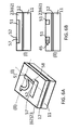
- FIGS. 5A-5B illustrate the formation of a probe body and a frame.
- FIGS. 6A-6B illustrate a second sacrificial layer formed on the probe in a planarization process.
- FIGS. 7A-7B illustrate the removal of the first sacrificial layer.
- FIGS. 8A-8B illustrate an alternative process in which an opening is formed in the first sacrificial layer.
- FIGS. 9A-9B illustrate the formation of the tip base and the frame in the alternative process.
- FIGS. 10A-10B illustrate the formation of the contact tip in the alternative process.
- FIGS. 11A-11B illustrate the formation of the probe body in the alternative process.
- FIGS. 12A-12B illustrate a planarization process in the alternative process.
- FIGS. 13A-13B illustrate the removal of the first sacrificial layer in the alternative process.
- FIG. 14 illustrates a structure of a probe.
- FIGS. 15A-15B illustrates probes having thickness variation in the base portion.
- FIG. 16 illustrates a probe having a corrugated base.
- FIG. 17 illustrates a probe having two stages of spring reactions.
- FIGS. 18( a )-( f ) illustrate variations of probe designs.
- FIGS. 19( a )-( e ) illustrate additional variations of probe designs.
- MEMS Micro-Electro-Mechanical Systems
- a probe card A technique for fabricating a Micro-Electro-Mechanical Systems (MEMS) probe on a substrate for use on another platform, such as a probe card, is described.
- MEMS Micro-Electro-Mechanical Systems
- Each probe includes a contact tip and a probe body.
- the probe body further includes a tip portion, a spring portion and a base portion.
- the probe is formed in a “lying” position, which means that the probe body is lying on a plane parallel with the surface of the substrate.
- the probe is detached from the substrate by forming an undercut beneath the probe and breaking the base portion from an anchoring structure on the substrate.
- the probe is then attached to an application platform of a probe card. During the attachment process, the probe is lifted up to a “standing” position such that only the base portion of the probe body is attached to the application platform.
- a pick-and-place process In one embodiment, a pick-and-place process is described.
- MEMS probes or “probes” are individually detached (“picked”) from a substrate, and then attached (“placed”) to an application platform in an unpackaged state.
- This “pick-and-place” technique not only improves the yield of the probes, but also greatly increases the flexibility with respect to how the MEMS probes are fabricated and used.
- the array of MEMS probes may be detached from the substrate concurrently, or one or more parts at a time.
- Each of the MEMS probes may be attached to the same or different application platforms.
- the MEMS probes attached to the same application platform may be fabricated on the substrate in a first arrangement and then attached to the application platform in a second arrangement, where the first arrangement and the second arrangement may have different spacing between the MEMS probes, different orientations of the MEM probes, or a combination of both.
- yield of the individual MEMS probes does not directly affect the yield of the final product.
- a selection process of acceptable MEMS probes may be performed before the MEMS probes are assembled on the probe cards.
- Defective MEMS probes may be discarded before the attachment process, or left on the substrate.
- MEMS probe refers to a probe fabricated by MEMS technology. It is understood that the technique described herein can be applied to other MEMS parts (e.g., mechanical parts, optical parts, electrical parts, or the like). Typically, a MEMS part has dimensions ranging from 10 ⁇ 10 ⁇ 10 ⁇ m to 5000 ⁇ 5000 ⁇ 5000 ⁇ m. Examples of a MEMS part include a probe, a laser module, optical lenses, micro-gears, micro-resistors, micro-capacitors, micro-inductors, micro-diaphragms, micro-relays, micro-springs, waveguides, micro-grooves, and the like.
- substrate refers to the substrate used in the probe fabrication process, without involvement in the operations of the probes and the probe card.
- a substrate for fabricating MEMS probes include, but are not limited to, ceramics, glasses, metal plates, plastic plates, and semiconductor (e.g., silicon (Si)) wafers.
- Si silicon
- a non-silicon substrate compared to a Si-based substrate, offers a larger number of standard sizes and is available as a thicker and non-circular standard substrate. Further, some non-silicon substrates are inert to most chemicals used during fabrication processes. Most substrates, including a Si-based substrate, can be processed with the MEMS parts thereon. Processed materials on the substrates can be later removed or dissolved without damaging the substrates.
- the substrate for fabricating MEMS probes is a “reusable substrate,” unless otherwise indicated.
- a reusable substrate can be reused for a next batch of MEMS probes fabrication after the MEMS probes are detached therefrom and residual substances are removed.
- an application platform refers to a part of a probe card which provides a platform to which the probes are attached, and electrically connects one or more (e.g., each) of the probes to a printed circuit board (PCB) that interfaces an electronic test system.
- An application platform may include, but is not limited to, semiconductor, glass, ceramics (e.g., low-temperature co-fired ceramics (LTCC), high-temperature co-fired ceramics (HTCC)), metal, other dielectric materials, organic materials, or any combinations of the above.
- LTCC low-temperature co-fired ceramics
- HTCC high-temperature co-fired ceramics
- an application platform may include components such as electrical connection, electrical contact, electrical isolation, electrical grounding, integrated circuit (IC) module, application specific IC (ASIC) module, dielectric patterning, conducting opening definition, mechanical support, mechanical protection, thermal conduction, electrostatic discharge (ESD) protection, confinement for parts, and wire bonding pads.
- IC integrated circuit
- ASIC application specific IC
- a probe card may include one or more MEMS probes fabricated from one or more reusable substrates.
- the MEMS probes attached to a probe card may be of different orientations, shapes, sizes and materials. The location of the probes on the probe card can be customized.
- FIGS. 1-7 an embodiment of a process for fabricating a MEMS probe on a substrate is shown in both perspective views and cross-section views. All of the figures labeled with “A” show perspective views, and all of the figures labeled with “B” show cross-section views. Although only one MEMS probe is shown in the figures, it is understood that the same process can be applied to the fabrication of an array of MEMS probes. Some standard or routine processing operations that are not directly relevant to the subject matter of the present invention, but are easily understood by a person of ordinary skill in the art, may be omitted from the following descriptions.
- FIGS. 1A and 1B show a blanket metal layer 12 (e.g., gold or other conductive material(s)) formed on a substrate 11 .
- the bottom of blanket metal layer 12 may be coated with a thin film (e.g., less than 1 micron, not shown), also referred to as a seed layer, that is made of a conductive material (e.g., a combination of chromium and gold) different from that of blanket metal layer 12 .
- blanket metal layer 12 is deposited by an electrical forming process (also know as electrodeposition), such as electrode plating.
- the seed layer is formed by a thin film deposition process, which can be thermal evaporation, e-beam evaporation, sputtering deposition, or the like.
- first sacrificial layer 23 is formed on metal blanket layer 12 ( FIGS. 2A and 2B ).
- First sacrificial layer 23 is a layer of metal (e.g., copper) or alloy, different from blanket metal layer 12 and the probe to be formed on substrate 11 .
- One way to form first sacrificial layer 23 is by electrical forming.
- first sacrificial layer 23 is to be removed from beneath the probe.
- first sacrificial layer 23 may be planarized before further processing operations are performed. Planarization may be performed by a machine, such as a lapping machine, a diamond fly-cutter, or the like.
- FIGS. 3A and 3B show a tip base 34 formed on top of first sacrificial layer 23 .
- tip base 34 is formed by using a first lithographic patterned mold (e.g., a photoresist mold) (not shown) to define the shape of tip base 34 .
- the first lithographic patterned mold is placed on first sacrificial layer 23 and filled, by electrical forming, with a metal (e.g., nickel) or alloy material.
- the first lithographic patterned mold is to be removed in a subsequent processing operation, e.g., after tip base 34 , the contact tip of the probe, or the probe is formed.
- FIGS. 4A and 4B show a contact tip 45 formed on tip base 34 , with a portion of contact tip 45 protruding from tip base 34 .
- contact tip 45 is formed by using a second lithographic patterned mold (e.g., a photoresist mold) (not shown) to define the shape of contact tip 45 .
- the second lithographic patterned mold is filled, by electrical forming, with a metal (e.g., rhodium) or alloy material different from the material of tip base 34 .
- the second lithographic patterned mold is also to be removed in a subsequent processing operation, e.g., after contact tip 45 or the probe is formed.
- tip base 34 and contact tip 45 are part of a probe 51 formed on substrate 11 .
- the rest of probe 51 and a frame 57 attaching to probe 51 are formed on substrate 11 .
- both tip base 34 and the rest of probe 51 are formed by the same material (e.g., nickel)
- tip base 34 becomes part of probe 51 and is not explicitly shown in FIG. 5A .
- probe 51 is formed in a “lying” position, which means that probe 51 is lying on a plane parallel with the surface of substrate 11 .
- FIG. 5B shows the cross-section view of probe 51 along axis (I) and axis (II).
- a thickness dimension, t of probe 51 is shown to be perpendicular to the surface of substrate 11 .
- Axis (I) extends along the longitudinal direction of an elongated section of probe 51 , referred to as a probe base 58 .
- a surface of probe base 58 referred to as a bonding surface 59 , lies on a plane along the thickness dimension and is perpendicular to the surface of substrate 11 .
- Axis (II) extends from probe base 58 to contact tip 45 and is parallel with the surface of substrate 11 . This “lying” position is opposed to a “standing” position when probe 51 is attached to an application platform of a probe card. In the “standing” position, bonding surface 59 is attached to the surface of the application platform, while contact tip 45 is lifted up such that axis (II) goes through the surface of the application platform.
- a thin metal film e.g. gold
- a thin metal film can be deposited at this point on the bonding surface 59 for the purpose of improving adhesion between probe base 58 to the surface of the application platform.
- Frame 57 (also referred to as an “island” or an “anchoring structure”) is used to anchor probe 51 to a fixed location on substrate 11 .
- frame 57 becomes the only support for probe 51 to remain on substrate 11 .
- the surface area of frame 57 is greater than that of probe 51 .
- a surface area ratio of frame 57 to probe 51 ranges from 25:1 (or more) to 2:1 (or less). Theoretically, there is no upper bound on this surface area ratio. However, a large surface area ratio means a large frame 57 on substrate 11 , and, therefore, less space for probes.
- the surface area ratio may depend on the relative shapes of frame 57 and probe 51 .
- the surface area ratio may be greatly reduced (e.g., 5:1, 2:1, 1:1, or less) if frame 57 has a substantially round shape and probe 51 has a long and narrow shape.
- a round-shaped frame 57 may have less surface area than a long and narrow probe 51 .
- the surface area ratio may increase (e.g., greater than 1:1, 5:1, 7:1, 10:1 or greater) if both frame 57 and probe 51 have a substantially same shape.
- the surface area ratio and the relative shapes (of frame 57 and probe 51 ) contribute to the differential etching rates of first sacrificial layer 23 underneath probe 51 and frame 57 , which is a feature that facilitates the detachment of probe 51 , as will be described in detail later with reference to FIGS. 7A and 7B .
- Probe 51 (excluding tip base 34 and contact tip 45 ) and frame 57 may be formed by using a third lithographic patterned mold (not shown) that defines the shapes of probe 51 and frame 57 .
- the third lithographic patterned mold is filled, by electrical forming, with a conductive material, such as a metal (e.g., nickel) or alloy.
- a conductive material such as a metal (e.g., nickel) or alloy.
- the first, second and third lithographic patterned molds may be made of the same materials, such as photoresist, or different materials.
- the third lithographic patterned mold also defines the shape of an anchoring joint 52 between probe base 58 and frame 57 .
- Anchoring joint 52 is shaped to have deep V-cuts on both sides of the joint section that connects probe base 58 and frame 57 .
- the cross-section of anchoring joint 52 (defined by a plane that cuts through the joint section of probe base 58 and frame 57 ) is a thin and narrow area.
- anchoring joint 52 is shaped to have deep V-cuts on both sides, such that its cross-section has substantially the shape of a line, which extends along the thickness of the probe layer.
- the shape of anchoring joint 52 facilitates the detachment of probe 51 from frame 57 by external force.
- a planarization operation is performed on probe 51 to control the thickness of probe 51 ( FIGS. 6A and 6B ).
- Frame 57 may be planarized with probe 51 at the same time.
- planarization can be performed to produce substantially equal thickness (within the design specification) across all of the probes on substrate 11 .
- Planarization may produce a shear force on probe 51 to cause damage to probe 51 .
- the third lithographic patterned mold may be kept on substrate 11 during the planarization, and stripped or dissolved away after the planarization.
- the third lithographic patterned mold is removed after the formation of probe 51 , and a second sacrificial layer 62 is applied as a blanket layer over probe 51 and the exposed surface of substrate 11 .
- Second sacrificial layer 62 may be made of the same material as any of the previous-applied lithographic patterned molds, the same conductive material as first sacrificial layer 23 (e.g., copper or alloy), or photoresist. In the embodiment shown in FIGS. 6A and 6B , second sacrificial layer 62 is the same material as first sacrificial layer 23 .
- second sacrificial layer 62 is stripped or dissolved.
- second sacrificial layer 62 is made of the same material as first sacrificial layer 23
- both of the first and second sacrificial layers 23 , 62 can be selectively etched or dissolved from beneath probe 51 .
- the selective removal creates an undercut 73 beneath probe 51 ( FIGS. 7A and 7B ).
- the surface areas and/or the shapes of frame 57 and probe 51 (as shown in FIG. 5A ) enables first sacrificial layer 23 underneath probe 51 to be etched faster than first sacrificial layer 23 underneath frame 57 .
- first sacrificial layer 23 When first sacrificial layer 23 is completely removed from underneath the probe 51 , there remains a substantial amount of first sacrificial layer 23 underneath frame 57 to hold frame 57 on substrate 11 . At this point, probe 51 is held in place, by frame 57 only, at anchoring joint 52 .
- a thin metal film e.g., gold
- the thin metal film may be deposited at this point instead of before the planarization operation.
- probe 51 is ready to be detached from frame 57 manually or with a machine.
- a lateral force (with respect to the surface of substrate 11 ) applied to probe 51 near anchoring joint 52 can separate probe 51 from frame 57 right at anchoring joint 52 .
- an upward swing force can be applied to or near anchoring point 52 to separate probe 51 from frame 57 .
- Yet another way of separating probe 51 from frame 57 is by laser cutting anchoring joint 52 .
- Substrate 11 is left with frame 57 after all probes 51 are detached.
- Substrate 11 can be reused for fabrication of a next batch of probes by continuing etching or dissolving first sacrificial layer 23 until frame 57 is separated from substrate 11 .
- Substrate 11 can then be reused with blanket metal layer 12 or the thin film at the bottom of blanket metal layer 12 , which remain on substrate 11 .
- the detachment of probe 51 can be performed by external force at or near anchoring joint 52 , with respect to the surface of substrate 11 .
- the external force either laterally or upward, or by laser cutting, physically breaks the narrow connection at anchoring joint 52 .
- a “broken” surface is formed on the side of probe base 58 that was previously connected to frame 57 .
- This broken surface is distinguishable from a surface defined by conventional methods of probe formation that does not use external force to detach a probe from the substrate.
- a surface formed by conventional methods is smooth and regularly shaped.
- a surface formed by forcibly breaking (such as the broken surface of probe base 58 ) is generally rough and substantially irregular.
- FIGS. 8A and 8B After blanket metal layer 12 is formed on substrate 11 , a photoresist pattern of opening 81 is formed before first sacrificial layer 23 is electrically formed. After first sacrificial layer 23 is formed, the photoresist is stripped to expose, through an opening 81 , blanket metal layer 12 or a thin film (also referred to as a seed layer, not shown) at the bottom of blanket metal layer 12 .
- a first lithographic patterned mold (not shown) is used to define the shape of tip base 34 and frame 92 ( FIGS. 9A and 9B ). Frame 92 is different from frame 57 ( FIGS.
- frame 92 has direct contact with blanket metal layer 12 or the seed layer at the bottom of blanket metal layer 12 , while frame 57 is formed on top of first sacrificial layer 23 without direct contact with blanket metal layer 12 or the seed layer.
- frame 92 and tip base 34 are formed, by electrical forming, for the same period of time.
- the thickness of tip base 34 and frame 92 is substantially the same.
- the center area of frame 92 forms a recess 93 .
- recess 93 may be removed by planarization.
- FIGS. 10A and 10B show that contact tip 45 is formed on top of probe base 34 .
- FIGS. 11A and 11B show that the rest of probe 51 is formed with frame 92 attaching to probe 51 .
- a second lithographic patterned mold and a third lithographic patterned mold may be used to form contact tip 45 , probe 51 and frame 92 .
- Frame 92 at this point is anchored to blanket metal layer 12 or the seed layer at the bottom of blanket metal layer 12 .
- Additional processes may be performed to apply a metal thin film (e.g., gold) to the bonding surface 59 of probe base 58 for the purpose of improving adhesion between probe base 58 to the surface of the platform of the probe card.
- a metal thin film e.g., gold
- FIGS. 12A and 12B show the planarization of the probe surface with the use of second sacrificial layer 62 , which, in this embodiment, is made of the same material as first sacrificial layer 23 .
- second sacrificial layer 62 may alternatively be made of photoresist, or the same material as any of the previously-applied lithographic patterned molds.
- first sacrificial layer 23 is etched or dissolved.
- frame 92 is anchored to blanket metal layer 12 or the seed layer at the bottom of blanket metal layer 12 , so complete removal of first sacrificial layer 23 does not create a problem.
- the removal of first sacrificial layer 23 creates an undercut 37 beneath probe 51 . Similar to the process described in FIGS. 7A and 7B , probe 51 can be detached from frame 92 by applying a physical force. Substrate 11 can be reused after frame 92 is etched or dissolved away.
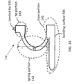
- the basic structure of a probe 140 (e.g., probe 51 ) includes a contact tip 145 and a probe body.
- the probe body further includes three main portions, a base portion 141 , a spring portion 142 and a tip portion 143 .
- Base portion 141 mechanically supports the rest of the probe structure and includes a bonding surface 144 at the bottom for attachment to a probe card.
- Spring portion 142 is designed to have a spring constant as specified by customer's requirements.
- Tip portion 143 supports contact tip 145 to form a contact to the device-under-test (DUT). All of the three portions ( 141 , 142 and 143 ) and contact tip 145 can be customized to satisfy the requirements of different applications.
- Spring portion 142 reacts with a buckling force to a pressure applied on tip portion 143 .
- spring portion 142 has a shape of a fraction of a circle or a deformed circle (e.g., a half circle, a half ellipse, a quarter ellipse, or a quarter circle), with one end extended to tip portion 143 and the other end anchored to base portion 141 .
- Spring portion 142 can also be designed such that its width (shown as “W” in FIG. 14 ) varies along the spring length (shown as “L”) to result in an optimized scrubbing mark.
- the shape of spring portion 142 is defined by one lithographic mold (the third lithographic patterned mold as described above) and formed in one lithographic operation (e.g., the processes described in FIGS. 5 and 11 above), the shape of spring portion 142 can be designed to have smooth curves or other geometrical shapes in the vertical direction (with respect to the surface of the probe card). Conventional processes create a spring vertically with respect to the surface of the probe card. Thus, multiple lithographic operations are necessary to pile and connect every layer that forms the spring. The final spring structure becomes jagged and has no smooth transition among the layers.
- the probe structure described herein is formed by at least three separate lithographic processes that form the tip base, the contact tip, and the rest of the probe body.
- the three lithographic processes allow the probe body to have thickness variations along its cross sections, wherein the thickness is measured in a direction perpendicular to the surface of substrate 11 .
- a metal or alloy material can be deposited in a recess section 150 of the probe body ( FIGS. 15A and 15B ).
- section 150 is covered with photoresist. After the photoresist is stripped, section 150 ends up having a thickness of the tip base layer only.
- recess section 151 of FIG. 15B can be formed to confine the bonding material when the probe is bonded to the application platform of the probe card. More lithographic steps can be introduced to further increase thickness variation along the probe if necessary.
- a probe 160 has a base portion 161 that is “corrugated” to improve the fitting and bonding to the application platform, which may have a counterpart corrugated design.
- a probe 170 has a stop 171 to provide two stages of buckling reactions. Initially, when the tip end of probe 170 was pressured downward, the whole spring of probe 170 reacts with an entire buckling force. If the downward pressure continues such that stop 171 hits the spring portion of probe 170 , only the top part of the spring portion reacts to the downward pressure. The two stages of buckling reactions produce different combination of vertical and lateral motions at the tip portion of probe 170 . The lateral and vertical motions of the tip portion, in turn, produce a scrubbing mark on the device-under-test (DUT).
- DUT device-under-test
- a desired buckling force can be produced by adjusting design factors such as probe height, probe thickness, stop position and stop gap (which is the gap or distance between stop 171 and spring portion of probe 170 ).
- Additional examples of probe springs include a buckling spring ( FIG. 18( a )), a snake shape spring ( FIG. 18( b )), a square spring ( FIG. 18( c )), a curve-up spring ( FIG. 18( d )), a curve-down spring ( FIG. 18( e )), and two-spring probe ( FIG. 18( f )).
- FIGS. 19( a )-( e ) illustrate more spring shapes that can be fabricated by the process described herein.
- a scrubbing mark is generally characterized by the length and depth of the mark on the DUT.
- the shape of contact tip 145 can be designed such that the scrubbing mark is optimized according to a specific application.
- Contact tip 145 is designed to be “sandwiched” by the metal layers of the probe body with a contact area exposed.
- the contact area has two parallel opposing sides (i.e., the upper and lower sides with respect to the surface of substrate 11 of FIG. 11A ).
- the front scrubbing edge of the contact area may have a sharp, pointed angle suitable for forming a desired scrubbing mark.
- the lithographic mold that is used for forming contact tip 45 (as in the processes described above with reference to FIGS. 4 and 10 ) can be designed such that the front scrubbing edge of contact tip 45 has a radius of curvature that is optimized for producing appropriate scrubbing pressure for probe card applications.
Landscapes
- Physics & Mathematics (AREA)
- General Physics & Mathematics (AREA)
- Geometry (AREA)
- Engineering & Computer Science (AREA)
- Manufacturing & Machinery (AREA)
- Computer Hardware Design (AREA)
- Microelectronics & Electronic Packaging (AREA)
- Power Engineering (AREA)
- Measuring Leads Or Probes (AREA)
- Testing Or Measuring Of Semiconductors Or The Like (AREA)
Priority Applications (5)
| Application Number | Priority Date | Filing Date | Title |
|---|---|---|---|
| US12/186,458 US8089294B2 (en) | 2008-08-05 | 2008-08-05 | MEMS probe fabrication on a reusable substrate for probe card application |
| TW098107009A TWI411783B (zh) | 2008-08-05 | 2009-03-04 | 微機電探針及其製作方法 |
| CN200910128922XA CN101644725B (zh) | 2008-08-05 | 2009-03-10 | 在可重复使用的基板上制造探针卡的微机电探针 |
| JP2009068075A JP2010038900A (ja) | 2008-08-05 | 2009-03-19 | プローブカードに応用するための再利用可能な基板上へのmemsプローブの製造方法 |
| KR1020090027205A KR101129624B1 (ko) | 2008-08-05 | 2009-03-31 | 프로브 카드 애플리케이션을 위한 재사용 가능한 기판 상의mems 프로브 제조 |
Applications Claiming Priority (1)
| Application Number | Priority Date | Filing Date | Title |
|---|---|---|---|
| US12/186,458 US8089294B2 (en) | 2008-08-05 | 2008-08-05 | MEMS probe fabrication on a reusable substrate for probe card application |
Publications (2)
| Publication Number | Publication Date |
|---|---|
| US20100033201A1 US20100033201A1 (en) | 2010-02-11 |
| US8089294B2 true US8089294B2 (en) | 2012-01-03 |
Family
ID=41652326
Family Applications (1)
| Application Number | Title | Priority Date | Filing Date |
|---|---|---|---|
| US12/186,458 Expired - Fee Related US8089294B2 (en) | 2008-08-05 | 2008-08-05 | MEMS probe fabrication on a reusable substrate for probe card application |
Country Status (5)
| Country | Link |
|---|---|
| US (1) | US8089294B2 (zh) |
| JP (1) | JP2010038900A (zh) |
| KR (1) | KR101129624B1 (zh) |
| CN (1) | CN101644725B (zh) |
| TW (1) | TWI411783B (zh) |
Cited By (3)
| Publication number | Priority date | Publication date | Assignee | Title |
|---|---|---|---|---|
| US9774117B1 (en) | 2016-03-22 | 2017-09-26 | Northrop Grumman Systems Corporation | Resilient miniature mechanical support that can also serve as an electrical connector |
| US9801269B1 (en) | 2016-05-10 | 2017-10-24 | Northrop Grumman Systems Corporation | Resilient miniature integrated electrical connector |
| TWI705249B (zh) * | 2014-12-30 | 2020-09-21 | 義大利商技術探測股份有限公司 | 包含用於測試頭的複數個接觸式探針的半完成產品及相關製造方法 |
Families Citing this family (18)
| Publication number | Priority date | Publication date | Assignee | Title |
|---|---|---|---|---|
| TW201135239A (en) * | 2010-04-02 | 2011-10-16 | Pleader Yamaichi Co Ltd | High-frequency vertical elastic probe structure |
| CN102486481B (zh) * | 2010-12-01 | 2014-08-06 | 励威电子股份有限公司 | 高频垂直式弹性探针结构 |
| JP5868239B2 (ja) * | 2012-03-27 | 2016-02-24 | 株式会社日本マイクロニクス | プローブ及びプローブカード |
| KR101299725B1 (ko) * | 2012-04-30 | 2013-08-28 | 디플러스(주) | 좌굴 프로브 핀 |
| CN116183986A (zh) * | 2014-12-30 | 2023-05-30 | 泰克诺探头公司 | 用于测试头的接触探针的制造方法 |
| TWI750721B (zh) * | 2015-12-28 | 2021-12-21 | 美商色拉頓系統公司 | 系統與觀察及測試受測試器件(DUTs)陣列之複數個探針模組之定位方法 |
| TWI598595B (zh) * | 2016-10-31 | 2017-09-11 | 穩懋半導體股份有限公司 | 改良式同軸探針結構 |
| US10782342B2 (en) * | 2016-11-21 | 2020-09-22 | Si-Ware Systems | Integrated optical probe card and system for batch testing of optical MEMS structures with in-plane optical axis using micro-optical bench components |
| CN108663553B (zh) * | 2017-03-29 | 2022-01-25 | 上海中船电气有限公司 | 一种接触式半导体材料测试头 |
| KR101958351B1 (ko) * | 2017-08-04 | 2019-03-15 | 리노공업주식회사 | 검사프로브 및 이를 사용한 검사장치 |
| JP2019160937A (ja) * | 2018-03-09 | 2019-09-19 | 東京エレクトロン株式会社 | 位置補正方法、検査装置及びプローブカード |
| KR102068699B1 (ko) * | 2018-08-24 | 2020-01-21 | 주식회사 에스디에이 | 레이저를 이용한 반도체 검사용 멤스 프로브의 제조방법 |
| EP3651479B1 (de) | 2018-11-08 | 2022-06-01 | Usound GmbH | Herstellungsverfahren für zumindest eine membraneinheit eines mems-wandlers |
| JP1646397S (zh) * | 2019-05-21 | 2019-11-25 | ||
| KR102388030B1 (ko) * | 2020-07-15 | 2022-04-20 | (주)엠투엔 | 프로브 핀, 이를 제조하는 방법 및 이를 구비하는 프로브 카드 |
| CN111983272B (zh) * | 2020-08-14 | 2021-02-12 | 强一半导体(苏州)有限公司 | 一种导引板mems探针结构制作方法 |
| CN116223866B (zh) * | 2023-05-10 | 2023-08-01 | 上海泽丰半导体科技有限公司 | 一种模块化探针卡及探针卡制造方法 |
| CN116430088B (zh) * | 2023-06-13 | 2023-11-24 | 南方科技大学 | 探针及其制备方法 |
Citations (59)
| Publication number | Priority date | Publication date | Assignee | Title |
|---|---|---|---|---|
| US4151945A (en) | 1977-12-08 | 1979-05-01 | Universal Instruments Corporation | Automated hybrid circuit board assembly apparatus |
| US4528500A (en) | 1980-11-25 | 1985-07-09 | Lightbody James D | Apparatus and method for testing circuit boards |
| US4773877A (en) | 1986-08-19 | 1988-09-27 | Feinmetall Gmbh | Contactor for an electronic tester |
| US4841240A (en) | 1988-01-29 | 1989-06-20 | American Telephone And Telegraph Company, At&T Bell Laboratories | Method and apparatus for verifying the continuity between a circuit board and a test fixture |
| US5100338A (en) | 1990-08-31 | 1992-03-31 | Foxconn International, Inc. | Contact for circuit board socket |
| US5177438A (en) | 1991-08-02 | 1993-01-05 | Motorola, Inc. | Low resistance probe for semiconductor |
| US5286208A (en) | 1991-02-19 | 1994-02-15 | Yamaichi Electric Co., Ltd. | Contact in electric part socket |
| US5465611A (en) | 1993-03-30 | 1995-11-14 | Imm Institut Fur Mikrotechnik Gmbh | Sensor head for use in atomic force microscopy and method for its production |
| US5798283A (en) | 1995-09-06 | 1998-08-25 | Sandia Corporation | Method for integrating microelectromechanical devices with electronic circuitry |
| US6359455B1 (en) | 1999-02-25 | 2002-03-19 | Tokyo Electron Limited | Probing card |
| US20020080588A1 (en) | 1993-11-16 | 2002-06-27 | Formfactor, Inc. | Probe card assembly and kit, and methods of making same |
| US20020163051A1 (en) | 2001-05-07 | 2002-11-07 | Applied Materials, Inc. | Microstructure devices, methods of forming a microstructure device and a method of forming a MEMS device |
| US6520778B1 (en) | 1997-02-18 | 2003-02-18 | Formfactor, Inc. | Microelectronic contact structures, and methods of making same |
| US6521970B1 (en) | 2000-09-01 | 2003-02-18 | National Semiconductor Corporation | Chip scale package with compliant leads |
| US20030046810A1 (en) | 2001-08-22 | 2003-03-13 | Farnworth Warren M. | Substrate mapping |
| US20030113990A1 (en) | 2001-12-19 | 2003-06-19 | Formfactor, Inc. | Microelectronic spring contact repair |
| US6672875B1 (en) | 1998-12-02 | 2004-01-06 | Formfactor, Inc. | Spring interconnect structures |
| US6680536B2 (en) | 2001-03-28 | 2004-01-20 | Yamaha Corporation | Probe unit having resilient metal leads |
| US6784680B2 (en) | 2000-06-01 | 2004-08-31 | Sumitomo Electric Industries, Ltd. | Contact probe with guide unit and fabrication method thereof |
| US6807734B2 (en) | 1998-02-13 | 2004-10-26 | Formfactor, Inc. | Microelectronic contact structures, and methods of making same |
| US20040245588A1 (en) | 2003-06-03 | 2004-12-09 | Nikkel Eric L. | MEMS device and method of forming MEMS device |
| US6861277B1 (en) | 2003-10-02 | 2005-03-01 | Hewlett-Packard Development Company, L.P. | Method of forming MEMS device |
| US20050176212A1 (en) | 2003-10-02 | 2005-08-11 | Monroe Michael G. | MEMS device and method of forming MEMS device |
| US6965245B2 (en) | 2003-05-01 | 2005-11-15 | K&S Interconnect, Inc. | Prefabricated and attached interconnect structure |
| US7048548B2 (en) | 1999-12-28 | 2006-05-23 | Formfactor, Inc. | Interconnect for microelectronic structures with enhanced spring characteristics |
| US7047638B2 (en) | 2002-07-24 | 2006-05-23 | Formfactor, Inc | Method of making microelectronic spring contact array |
| US20060134819A1 (en) | 2004-12-21 | 2006-06-22 | Integrated Micromachines, Inc. | Process for forming MEMS |
| US7078921B2 (en) | 2001-12-25 | 2006-07-18 | Sumitomo Electric Industries, Ltd. | Contact probe |
| US20060192581A1 (en) | 2002-02-05 | 2006-08-31 | Phicom Corporation | Method for manufacturing electrical contact element for testing electro device and electrical contact element thereby |
| US7151385B2 (en) | 2001-01-29 | 2006-12-19 | Sumitomo Electric Industries, Ltd. | Contact probe, method of manufacturing the contact probe, and device and method for inspection |
| US7156706B2 (en) | 2003-07-22 | 2007-01-02 | Tyco Electronics Corporation | Contact having multiple contact beams |
| US20070018666A1 (en) | 2005-07-22 | 2007-01-25 | Nasser Barabi | Spring contact pin for an IC chip tester |
| US7190179B2 (en) | 2001-04-13 | 2007-03-13 | Sumitomo Electric Industries, Ltd. | Contact probe |
| US7267557B2 (en) | 2005-02-03 | 2007-09-11 | Mjc Probe Incorporation | Micro contact device comprising the micro contact element and the base member |
| US7271022B2 (en) | 2004-12-21 | 2007-09-18 | Touchdown Technologies, Inc. | Process for forming microstructures |
| US7285966B2 (en) | 2003-03-17 | 2007-10-23 | Phicom Corporation | Probe and method of making same |
| US20070245552A1 (en) | 2006-04-07 | 2007-10-25 | John Caldwell | Probe interposers and methods of fabricating probe interposers |
| US20070256299A1 (en) | 2006-02-22 | 2007-11-08 | Dov Chartarifsky | Approach for fabricating cantilever probes |
| US20070290698A1 (en) | 2006-06-19 | 2007-12-20 | Tokyo Electron Limited | Probe card |
| US20080007282A1 (en) | 2006-06-26 | 2008-01-10 | Kabushiki Kaisha Nihon Micronics | Probe assembly |
| US20080036449A1 (en) | 2006-08-08 | 2008-02-14 | Gunsei Kimoto | Coordinate transforming apparatus for electrical signal connection |
| US7349223B2 (en) | 2000-05-23 | 2008-03-25 | Nanonexus, Inc. | Enhanced compliant probe card systems having improved planarity |
| US20080111573A1 (en) | 2003-02-04 | 2008-05-15 | Microfabrica Inc. | Pin-Type Probes for Contacting Electronic Circuits and Methods for Making Such Probes |
| US20080115353A1 (en) | 1998-12-02 | 2008-05-22 | Formfactor, Inc. | Lithographic contact elements |
| US7377788B2 (en) | 2004-01-16 | 2008-05-27 | Kabushiki Kaisha Nihon Micronics | Electrical connecting apparatus and contact |
| US20080184559A1 (en) | 2007-02-06 | 2008-08-07 | Kabushiki Kaisha Nihon Micronics | Method for manufacturing a probe |
| US20090040911A1 (en) * | 2007-08-10 | 2009-02-12 | Tsung-Kuan Allen Chou | Cantilever on cantilever structure |
| US7503811B2 (en) | 2003-02-28 | 2009-03-17 | Phicom Corporation | Interconnection device for a printed circuit board, a method of manufacturing the same, and an interconnection assembly having the same |
| US7511523B2 (en) * | 2003-02-04 | 2009-03-31 | Microfabrica Inc. | Cantilever microprobes for contacting electronic components and methods for making such probes |
| US20090144970A1 (en) | 2007-12-06 | 2009-06-11 | Winmems Technologies Holdings Co., Ltd. | Fabricating an array of mems parts on a substrate |
| US7553165B2 (en) | 1998-12-02 | 2009-06-30 | Formfactor, Inc. | Spring interconnect structures |
| US7567089B2 (en) | 2003-02-04 | 2009-07-28 | Microfabrica Inc. | Two-part microprobes for contacting electronic components and methods for making such probes |
| US7586321B2 (en) | 2006-09-26 | 2009-09-08 | Kabushiki Kaisha Nihon Micronics | Electrical test probe and electrical test probe assembly |
| US7633306B2 (en) | 2003-03-14 | 2009-12-15 | Rudolph Technologies, Inc. | System and method of measuring probe float |
| US7644490B1 (en) | 2007-05-25 | 2010-01-12 | National Semiconductor Corporation | Method of forming a microelectromechanical (MEMS) device |
| US7714235B1 (en) | 1997-05-06 | 2010-05-11 | Formfactor, Inc. | Lithographically defined microelectronic contact structures |
| US7737714B2 (en) | 2008-11-05 | 2010-06-15 | Winmems Technologies Holdings Co., Ltd. | Probe assembly arrangement |
| US7776631B2 (en) | 1994-05-05 | 2010-08-17 | Qualcomm Mems Technologies, Inc. | MEMS device and method of forming a MEMS device |
| US7811849B2 (en) | 2008-01-30 | 2010-10-12 | Winmems Technologies Co., Ltd. | Placing a MEMS part on an application platform using a guide mask |
Family Cites Families (11)
| Publication number | Priority date | Publication date | Assignee | Title |
|---|---|---|---|---|
| JPH11271015A (ja) * | 1998-03-23 | 1999-10-05 | Olympus Optical Co Ltd | 走査型プローブ顕微鏡用カンチレバーチップ及びその製造方法 |
| TW546478B (en) * | 2002-01-08 | 2003-08-11 | Ind Tech Res Inst | Suspension-arm type testing card and its manufacturing method |
| US7122760B2 (en) * | 2002-11-25 | 2006-10-17 | Formfactor, Inc. | Using electric discharge machining to manufacture probes |
| EP1548748A1 (en) * | 2003-12-17 | 2005-06-29 | Interuniversitaire Microelectronica Centrum vzw ( IMEC) | A method for making probes for atomic force microscopy |
| KR100670999B1 (ko) * | 2004-11-24 | 2007-01-17 | 세크론 주식회사 | 프로브 구조, 프로브 콘택 기판 및 그 제조 방법 |
| CN100516885C (zh) * | 2005-03-22 | 2009-07-22 | 旺矽科技股份有限公司 | 弹性微接触元件及其制造方法 |
| TWI282424B (en) * | 2005-12-30 | 2007-06-11 | Advanced Semiconductor Eng | MEMS type probe card with multi-layer elasticity |
| CN1866407A (zh) * | 2006-05-31 | 2006-11-22 | 北京大学 | Mems力学微探针及其制备方法 |
| KR20070117974A (ko) * | 2006-06-10 | 2007-12-13 | 김상훈 | 마이크로 프로브 제조 |
| CN101131400A (zh) * | 2006-08-21 | 2008-02-27 | 南茂科技股份有限公司 | 合金探针的微机电制造方法 |
| JP4916893B2 (ja) * | 2007-01-05 | 2012-04-18 | 株式会社日本マイクロニクス | プローブの製造方法 |
-
2008
- 2008-08-05 US US12/186,458 patent/US8089294B2/en not_active Expired - Fee Related
-
2009
- 2009-03-04 TW TW098107009A patent/TWI411783B/zh not_active IP Right Cessation
- 2009-03-10 CN CN200910128922XA patent/CN101644725B/zh not_active Expired - Fee Related
- 2009-03-19 JP JP2009068075A patent/JP2010038900A/ja active Pending
- 2009-03-31 KR KR1020090027205A patent/KR101129624B1/ko not_active IP Right Cessation
Patent Citations (67)
| Publication number | Priority date | Publication date | Assignee | Title |
|---|---|---|---|---|
| US4151945A (en) | 1977-12-08 | 1979-05-01 | Universal Instruments Corporation | Automated hybrid circuit board assembly apparatus |
| US4528500A (en) | 1980-11-25 | 1985-07-09 | Lightbody James D | Apparatus and method for testing circuit boards |
| US4773877A (en) | 1986-08-19 | 1988-09-27 | Feinmetall Gmbh | Contactor for an electronic tester |
| US4841240A (en) | 1988-01-29 | 1989-06-20 | American Telephone And Telegraph Company, At&T Bell Laboratories | Method and apparatus for verifying the continuity between a circuit board and a test fixture |
| US5100338A (en) | 1990-08-31 | 1992-03-31 | Foxconn International, Inc. | Contact for circuit board socket |
| US5286208A (en) | 1991-02-19 | 1994-02-15 | Yamaichi Electric Co., Ltd. | Contact in electric part socket |
| US5177438A (en) | 1991-08-02 | 1993-01-05 | Motorola, Inc. | Low resistance probe for semiconductor |
| US5465611A (en) | 1993-03-30 | 1995-11-14 | Imm Institut Fur Mikrotechnik Gmbh | Sensor head for use in atomic force microscopy and method for its production |
| US20020080588A1 (en) | 1993-11-16 | 2002-06-27 | Formfactor, Inc. | Probe card assembly and kit, and methods of making same |
| US7776631B2 (en) | 1994-05-05 | 2010-08-17 | Qualcomm Mems Technologies, Inc. | MEMS device and method of forming a MEMS device |
| US5798283A (en) | 1995-09-06 | 1998-08-25 | Sandia Corporation | Method for integrating microelectromechanical devices with electronic circuitry |
| US6520778B1 (en) | 1997-02-18 | 2003-02-18 | Formfactor, Inc. | Microelectronic contact structures, and methods of making same |
| US7714235B1 (en) | 1997-05-06 | 2010-05-11 | Formfactor, Inc. | Lithographically defined microelectronic contact structures |
| US6807734B2 (en) | 1998-02-13 | 2004-10-26 | Formfactor, Inc. | Microelectronic contact structures, and methods of making same |
| US7553165B2 (en) | 1998-12-02 | 2009-06-30 | Formfactor, Inc. | Spring interconnect structures |
| US7555836B2 (en) | 1998-12-02 | 2009-07-07 | Formfactor, Inc. | Method of making lithographic contact elements |
| US6672875B1 (en) | 1998-12-02 | 2004-01-06 | Formfactor, Inc. | Spring interconnect structures |
| US20080115353A1 (en) | 1998-12-02 | 2008-05-22 | Formfactor, Inc. | Lithographic contact elements |
| US6359455B1 (en) | 1999-02-25 | 2002-03-19 | Tokyo Electron Limited | Probing card |
| US7048548B2 (en) | 1999-12-28 | 2006-05-23 | Formfactor, Inc. | Interconnect for microelectronic structures with enhanced spring characteristics |
| US7349223B2 (en) | 2000-05-23 | 2008-03-25 | Nanonexus, Inc. | Enhanced compliant probe card systems having improved planarity |
| US6784680B2 (en) | 2000-06-01 | 2004-08-31 | Sumitomo Electric Industries, Ltd. | Contact probe with guide unit and fabrication method thereof |
| US6521970B1 (en) | 2000-09-01 | 2003-02-18 | National Semiconductor Corporation | Chip scale package with compliant leads |
| US7151385B2 (en) | 2001-01-29 | 2006-12-19 | Sumitomo Electric Industries, Ltd. | Contact probe, method of manufacturing the contact probe, and device and method for inspection |
| US6680536B2 (en) | 2001-03-28 | 2004-01-20 | Yamaha Corporation | Probe unit having resilient metal leads |
| US7190179B2 (en) | 2001-04-13 | 2007-03-13 | Sumitomo Electric Industries, Ltd. | Contact probe |
| US20020163051A1 (en) | 2001-05-07 | 2002-11-07 | Applied Materials, Inc. | Microstructure devices, methods of forming a microstructure device and a method of forming a MEMS device |
| US20030046810A1 (en) | 2001-08-22 | 2003-03-13 | Farnworth Warren M. | Substrate mapping |
| US6555400B2 (en) | 2001-08-22 | 2003-04-29 | Micron Technology, Inc. | Method for substrate mapping |
| US20030113990A1 (en) | 2001-12-19 | 2003-06-19 | Formfactor, Inc. | Microelectronic spring contact repair |
| US7078921B2 (en) | 2001-12-25 | 2006-07-18 | Sumitomo Electric Industries, Ltd. | Contact probe |
| US20060192581A1 (en) | 2002-02-05 | 2006-08-31 | Phicom Corporation | Method for manufacturing electrical contact element for testing electro device and electrical contact element thereby |
| US20060191136A1 (en) | 2002-07-24 | 2006-08-31 | Formfactor, Inc. | Method Of Making Microelectronic Spring Contact Array |
| US7047638B2 (en) | 2002-07-24 | 2006-05-23 | Formfactor, Inc | Method of making microelectronic spring contact array |
| US7511523B2 (en) * | 2003-02-04 | 2009-03-31 | Microfabrica Inc. | Cantilever microprobes for contacting electronic components and methods for making such probes |
| US7567089B2 (en) | 2003-02-04 | 2009-07-28 | Microfabrica Inc. | Two-part microprobes for contacting electronic components and methods for making such probes |
| US20080111573A1 (en) | 2003-02-04 | 2008-05-15 | Microfabrica Inc. | Pin-Type Probes for Contacting Electronic Circuits and Methods for Making Such Probes |
| US7503811B2 (en) | 2003-02-28 | 2009-03-17 | Phicom Corporation | Interconnection device for a printed circuit board, a method of manufacturing the same, and an interconnection assembly having the same |
| US7633306B2 (en) | 2003-03-14 | 2009-12-15 | Rudolph Technologies, Inc. | System and method of measuring probe float |
| US7285966B2 (en) | 2003-03-17 | 2007-10-23 | Phicom Corporation | Probe and method of making same |
| US6965245B2 (en) | 2003-05-01 | 2005-11-15 | K&S Interconnect, Inc. | Prefabricated and attached interconnect structure |
| US20040245588A1 (en) | 2003-06-03 | 2004-12-09 | Nikkel Eric L. | MEMS device and method of forming MEMS device |
| US7156706B2 (en) | 2003-07-22 | 2007-01-02 | Tyco Electronics Corporation | Contact having multiple contact beams |
| US6861277B1 (en) | 2003-10-02 | 2005-03-01 | Hewlett-Packard Development Company, L.P. | Method of forming MEMS device |
| US20050176212A1 (en) | 2003-10-02 | 2005-08-11 | Monroe Michael G. | MEMS device and method of forming MEMS device |
| US20050106772A1 (en) | 2003-10-02 | 2005-05-19 | Monroe Michael G. | MEMS device and method of forming MEMS device |
| US7377788B2 (en) | 2004-01-16 | 2008-05-27 | Kabushiki Kaisha Nihon Micronics | Electrical connecting apparatus and contact |
| US7271022B2 (en) | 2004-12-21 | 2007-09-18 | Touchdown Technologies, Inc. | Process for forming microstructures |
| US20060134819A1 (en) | 2004-12-21 | 2006-06-22 | Integrated Micromachines, Inc. | Process for forming MEMS |
| US7267557B2 (en) | 2005-02-03 | 2007-09-11 | Mjc Probe Incorporation | Micro contact device comprising the micro contact element and the base member |
| US20070018666A1 (en) | 2005-07-22 | 2007-01-25 | Nasser Barabi | Spring contact pin for an IC chip tester |
| US7721430B2 (en) | 2006-02-22 | 2010-05-25 | Sv Probe Pte Ltd. | Approach for fabricating cantilever probes |
| US20070256299A1 (en) | 2006-02-22 | 2007-11-08 | Dov Chartarifsky | Approach for fabricating cantilever probes |
| US20070245552A1 (en) | 2006-04-07 | 2007-10-25 | John Caldwell | Probe interposers and methods of fabricating probe interposers |
| US20070290698A1 (en) | 2006-06-19 | 2007-12-20 | Tokyo Electron Limited | Probe card |
| US7474110B2 (en) | 2006-06-19 | 2009-01-06 | Tokyo Electron Limited | Probe card |
| US7532020B2 (en) | 2006-06-26 | 2009-05-12 | Kabushiki Kaisha Nihon Micronics | Probe assembly |
| US20080007282A1 (en) | 2006-06-26 | 2008-01-10 | Kabushiki Kaisha Nihon Micronics | Probe assembly |
| US20080036449A1 (en) | 2006-08-08 | 2008-02-14 | Gunsei Kimoto | Coordinate transforming apparatus for electrical signal connection |
| US7586321B2 (en) | 2006-09-26 | 2009-09-08 | Kabushiki Kaisha Nihon Micronics | Electrical test probe and electrical test probe assembly |
| US20080184559A1 (en) | 2007-02-06 | 2008-08-07 | Kabushiki Kaisha Nihon Micronics | Method for manufacturing a probe |
| US7721429B2 (en) | 2007-02-06 | 2010-05-25 | Kabushiki Kaisha Nihon Micronics | Method for manufacturing a probe |
| US7644490B1 (en) | 2007-05-25 | 2010-01-12 | National Semiconductor Corporation | Method of forming a microelectromechanical (MEMS) device |
| US20090040911A1 (en) * | 2007-08-10 | 2009-02-12 | Tsung-Kuan Allen Chou | Cantilever on cantilever structure |
| US20090144970A1 (en) | 2007-12-06 | 2009-06-11 | Winmems Technologies Holdings Co., Ltd. | Fabricating an array of mems parts on a substrate |
| US7811849B2 (en) | 2008-01-30 | 2010-10-12 | Winmems Technologies Co., Ltd. | Placing a MEMS part on an application platform using a guide mask |
| US7737714B2 (en) | 2008-11-05 | 2010-06-15 | Winmems Technologies Holdings Co., Ltd. | Probe assembly arrangement |
Non-Patent Citations (1)
| Title |
|---|
| Winmems Technologies Holdings Co, Final Office Action mailed Sep. 1, 2011 for U.S. Appl. No. 11/951,772., 14 pages. |
Cited By (5)
| Publication number | Priority date | Publication date | Assignee | Title |
|---|---|---|---|---|
| TWI705249B (zh) * | 2014-12-30 | 2020-09-21 | 義大利商技術探測股份有限公司 | 包含用於測試頭的複數個接觸式探針的半完成產品及相關製造方法 |
| US9774117B1 (en) | 2016-03-22 | 2017-09-26 | Northrop Grumman Systems Corporation | Resilient miniature mechanical support that can also serve as an electrical connector |
| US20170310028A1 (en) * | 2016-03-22 | 2017-10-26 | Northrop Grumman Systems Corporation | Resilient miniature mechanical support that can also serve as an electrical connector |
| US9837738B2 (en) * | 2016-03-22 | 2017-12-05 | Northrop Grumman Systems Corporation | Resilient miniature mechanical support that can also serve as an electrical connector |
| US9801269B1 (en) | 2016-05-10 | 2017-10-24 | Northrop Grumman Systems Corporation | Resilient miniature integrated electrical connector |
Also Published As
| Publication number | Publication date |
|---|---|
| US20100033201A1 (en) | 2010-02-11 |
| TWI411783B (zh) | 2013-10-11 |
| KR101129624B1 (ko) | 2012-03-27 |
| KR20100017042A (ko) | 2010-02-16 |
| JP2010038900A (ja) | 2010-02-18 |
| TW201007169A (en) | 2010-02-16 |
| CN101644725A (zh) | 2010-02-10 |
| CN101644725B (zh) | 2013-03-13 |
Similar Documents
| Publication | Publication Date | Title |
|---|---|---|
| US8089294B2 (en) | MEMS probe fabrication on a reusable substrate for probe card application | |
| US7928751B2 (en) | MEMS interconnection pins fabrication on a reusable substrate for probe card application | |
| US7737714B2 (en) | Probe assembly arrangement | |
| US6414501B2 (en) | Micro cantilever style contact pin structure for wafer probing | |
| TWI278627B (en) | A probe card manufacturing method including sensing probe and the probe card, probe card inspection system | |
| US20040119485A1 (en) | Probe finger structure and method for making a probe finger structure | |
| CN111137840B (zh) | 利用激光的半导体检查用微机电探针制备方法 | |
| US7548082B2 (en) | Inspection probe | |
| TWI553800B (zh) | 部分地埋置於層體結構內之微型彈簧 | |
| JP2009540291A (ja) | カンチレバー型プローブ製造方法及びこれを用いるプローブカード製造方法 | |
| KR100670999B1 (ko) | 프로브 구조, 프로브 콘택 기판 및 그 제조 방법 | |
| TWI502202B (zh) | 探針的製造方法 | |
| US20090144970A1 (en) | Fabricating an array of mems parts on a substrate | |
| TWI271379B (en) | Integrated probe module for LCD panel light inspection | |
| US7240428B2 (en) | Method for making probes for atomic force microscopy | |
| EP1544865B1 (en) | A method for making probes for atomic force microscopy | |
| KR100303536B1 (ko) | 고집적 미소커넥터 및 그 제조방법 | |
| EP1898223A1 (en) | Probe substrate for test and manufacturing method thereof | |
| KR100932104B1 (ko) | 사선형 탐침부재를 구비한 프로브 블록 및 상기탐침부재를 제조하는 방법 |
Legal Events
| Date | Code | Title | Description |
|---|---|---|---|
| AS | Assignment |
Owner name: WINMEMS TECHNOLOGIES HOLDINGS CO., LTD.,TAIWAN Free format text: ASSIGNMENT OF ASSIGNORS INTEREST;ASSIGNORS:HSU, TSENG-YANG;LAM, CAO NGOC;REEL/FRAME:021366/0252 Effective date: 20080805 Owner name: WINMEMS TECHNOLOGIES HOLDINGS CO., LTD., TAIWAN Free format text: ASSIGNMENT OF ASSIGNORS INTEREST;ASSIGNORS:HSU, TSENG-YANG;LAM, CAO NGOC;REEL/FRAME:021366/0252 Effective date: 20080805 |
|
| STCF | Information on status: patent grant |
Free format text: PATENTED CASE |
|
| AS | Assignment |
Owner name: WINMEMS TECHNOLOGIES CO., LTD., TAIWAN Free format text: ASSIGNMENT OF ASSIGNORS INTEREST;ASSIGNOR:WINMEMS TECHNOLOGIES HOLDINGS CO., LTD.;REEL/FRAME:027769/0420 Effective date: 20120224 |
|
| FPAY | Fee payment |
Year of fee payment: 4 |
|
| FEPP | Fee payment procedure |
Free format text: MAINTENANCE FEE REMINDER MAILED (ORIGINAL EVENT CODE: REM.); ENTITY STATUS OF PATENT OWNER: SMALL ENTITY |
|
| LAPS | Lapse for failure to pay maintenance fees |
Free format text: PATENT EXPIRED FOR FAILURE TO PAY MAINTENANCE FEES (ORIGINAL EVENT CODE: EXP.); ENTITY STATUS OF PATENT OWNER: SMALL ENTITY |
|
| STCH | Information on status: patent discontinuation |
Free format text: PATENT EXPIRED DUE TO NONPAYMENT OF MAINTENANCE FEES UNDER 37 CFR 1.362 |
|
| FP | Lapsed due to failure to pay maintenance fee |
Effective date: 20200103 |