EP1544865B1 - A method for making probes for atomic force microscopy - Google Patents
A method for making probes for atomic force microscopy Download PDFInfo
- Publication number
- EP1544865B1 EP1544865B1 EP04447272A EP04447272A EP1544865B1 EP 1544865 B1 EP1544865 B1 EP 1544865B1 EP 04447272 A EP04447272 A EP 04447272A EP 04447272 A EP04447272 A EP 04447272A EP 1544865 B1 EP1544865 B1 EP 1544865B1
- Authority
- EP
- European Patent Office
- Prior art keywords
- holder
- probe
- contact region
- substrate
- pads
- Prior art date
- Legal status (The legal status is an assumption and is not a legal conclusion. Google has not performed a legal analysis and makes no representation as to the accuracy of the status listed.)
- Not-in-force
Links
Images


Classifications
-
- G—PHYSICS
- G01—MEASURING; TESTING
- G01Q—SCANNING-PROBE TECHNIQUES OR APPARATUS; APPLICATIONS OF SCANNING-PROBE TECHNIQUES, e.g. SCANNING PROBE MICROSCOPY [SPM]
- G01Q60/00—Particular types of SPM [Scanning Probe Microscopy] or microscopes; Essential components thereof
- G01Q60/24—AFM [Atomic Force Microscopy] or apparatus therefor, e.g. AFM probes
- G01Q60/38—Probes, their manufacture, or their related instrumentation, e.g. holders
Landscapes
- Physics & Mathematics (AREA)
- Health & Medical Sciences (AREA)
- General Health & Medical Sciences (AREA)
- General Physics & Mathematics (AREA)
- Nuclear Medicine, Radiotherapy & Molecular Imaging (AREA)
- Radiology & Medical Imaging (AREA)
- Measuring Leads Or Probes (AREA)
- Testing Or Measuring Of Semiconductors Or The Like (AREA)
Description
- The present invention is related to probes for Atomic Force Microscopy (AFM). Such a probe consists of a probe tip, a cantilever and a probe holder chip. The invention is related to a method for manufacturing a probe of this type.
- Atomic Force Microscopy is a well established surface analysis technique for analysing the topography and electrical characteristics of semiconductor samples. The technique involves the use of a moving probe in contact with the surface under analysis. An AFM probe generally consists of a cantilever, a tip at one end of the cantilever and a holder at the other end. The holder is a large body of material used to handle the probe and is preferably located at the opposite side of the probe tip, i.e. at the side pointing in the opposite direction of the tip, this to prevent the holder from touching the sample's surface.
- A first type of probe, having a silicon tip, manufactured by Si bulk micromachining, is known in the art.
- The kind of probe to which the invention is related has a tip that is moulded into a silicon substrate. This is illustrated for example in document US-A-5399232. Of this type, probes with silicon nitride tip and cantilever are the most common. In all cases of this kind, the tip is pointing inwards towards the substrate. The holder can be attached by anodic bonding, or by adhesive, eutectic or solder bonding. It can be formed above the wafer by plating or out of thick resist. Often, a full glass wafer is bonded and then diced on the substrate to form individual holders.
- In any event, when making a probe with a moulded tip, it is necessary to release the probe from the substrate. The best known way to do this is to etch back all or a part of the silicon substrate from the back side, as described in US-A-5399232. However, this approach suffers from a number of disadvantages, most important of which are the long release time and the important loss of material by etching the entire thickness of the substrate.
- Another technique involves the peeling off of the probe, followed by the attachment of the holder, such as disclosed for example in EP-A-1202047. This is however a slow manual process. Also, inherent to the difficult process of bonding a holder to the probe after peel-off, the risk of breaking the probe is important. Finally, when applying this process, the holders must be attached one by one. Dicing a substrate above a number of peeled-off probes is not possible, because of the mechanical stress that would be applied to the holder-substrate, and the subsequent risk of damage to the probes.
- In the already cited EP-A-1202047, the probe tip and cantilever are underetched prior to peel-off, but the rest of the probe structure, particularly the part on which the holder is to be attached is too large to be fully underetched. This has also made it impossible so far to release the probe from the front side after bonding or forming of a holder. No sacrificial layer has been found to be really practical for release under a 1.5X3mm holder piece. Either the etch rate is too slow or the release chemical is overly harmful to the probe. Underetching the Si wafer under the probe is not an option either, since Si is etched slowly in KOH or another anisotropic etchant. Even when the probe is oriented along the fast underetched <100> direction, which is normally not the case, such an underetch would be slow and it is probable that the substrate is etched through before the underetch is complete. In order to reduce the underetching time of a sacrificial layer, it is known to produce small holes in the microfabricated structure to be released. However, this has so far not been done for a complete AFM probe, including the attached holder.
- Another example of top side release of a probe before holder attachment, in this case a diamond probe is to be found in 'CVD diamond probes for nanotechnology', Niedermann et al., Appl. Phys. A66, S31-S34 (1998). In this case, the film comprising the cantilever forms a pattern that is mostly in the <100> direction although the probe including the cantilever is still oriented in the general <110> direction. An example of front side release of patterned microstructures by underetching the Si substrate in isotropic etchant can be found in WO-A-9418697. In this case the pattern does not need to be rotated in the <100> direction Document US-A-6215137 is related to a probe with a thermocouple made of a joint between a first metal material and a second metal material. To release the probes, etching from the backside of the substrate is performed.
Document EP-A-1189016 is related to a soldering procedure, for mounting a probe to a holder chip, after the substrate carrying the probe has been etched from the backside of the substrate. - The present invention aims to provide a method for producing probes with a moulded tip, which does not suffer from the disadvantages of the prior art.
- The present invention is related to a method and a product having the characteristics described in the appended
independent claims - Fig. 1a represents in top view a preferred embodiment of a probe configuration used in the method of the invention. Figures 1b and 1c represent sectioned views of two alternatives, respectively with or without a sacrificial layer.
- Fig. 2 represents another probe configuration according to the invention.
- Fig. 3 and 4 represent probe configurations with three probe tips.
- Fig. 5 represents the way in which a holder substrate may be diced after attachment.
- Fig. 6a to 6c represents ways of increasing the gap between the holder and the substrate.
- Fig. 7 represents an alternative, involving a plated holder.
- Fig. 8 represents another alternative, involving a holder comprising holes through the thickness.
- The method of the invention comprises firstly a number of steps which are known from the prior art :
- providing a semiconductor substrate, preferably a Si substrate,
- producing on the surface of one side of the substrate, one or more moulds in the substrate. A mould is preferably a pyramidal pit, produced for example by the use of a hard mask, and an anisotropic etch, usually in KOH,
- optionally, applying a tip material, for example a metal, a hardmetal, a metal oxide, a ceramic or diamond. This is done when the tip material is different from the cantilever material.
- optionally, patterning the tip material. In some cases, the patterning can be done prior to the tip material deposition. In this case, a material is deposited and patterned. The tip material is then deposited selectively, See C. Mihalcea et Al, Appl. Phys. A 66, S87-S90 or W. Hanni et Al, Thin Solid Films 236, 87-90 (1993).
- Creating a probe configuration on the surface at the side of the mould, comprising a contact region for attachment of a holder, and at least one set of a probe tip and a cantilever. Different ways of creating such a probe configuration can be applied, as described further in this description. More than one probe configuration may be created simultaneously.
- attaching a holder to said contact region(s).
- According to the preferred embodiment, the probe configuration is made in such a way that the contact region consists of one or more separate, elevated bonding pads, the total surface of these pads being smaller than the surface area of the holder region which is to be attached to these pads. The holder is then attached to these pads, by a known technique, for example bonding or soldering.
- After this, the probe and holder are separated from the substrate by underetching with a release chemical from the front side of the substrate. The contact region can be fully underetched due to the reduced size of this contact region. The height of the pads must be sufficient to allow the release chemical to flow underneath the attached holder, into a gap formed between the holder and the substrate. The difference in size between the contact region and the holder needs to be sufficient in order to allow the creation of said gap over a large area of the substrate surface which is covered by the holder. In one specific embodiment, the pads are only surrounded by a gutter, and the gap is formed by the thickness of a bonding layer attached to the pads (see fig. 2).
- Optionally, a sacrificial layer may be applied before creating the probe configuration. Such a sacrificial layer will facilitate the release.
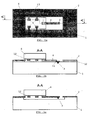
- Figure 1a illustrates a preferred embodiment of the invention. It shows a top view of the
substrate 1 wherein the probe configuration is equally visible. This configuration comprises the probe tip 3 (possibly made of a different material than the probe layer), thecantilever 4 and the contact region, comprising fourbonding pads 5. The large rectangle indicates the place where theholder 6 will be placed. Thepart 7 of the cantilever which is to be covered by the holder, can be viewed as a fifth bonding pad. Thebonding pads probe layer 2, and subsequently patterning this layer. - Figure 1b shows a first embodiment wherein a
sacrificial layer 10 is applied before applying theprobe layer 2. It is to be noted that the sacrificial layer is patterned prior to the application of the probe layer, so that asmall area 11 around the tip is not covered by said sacrificial layer. - Then the
probe layer 2 is applied on top of the sacrificial layer and subsequently patterned to obtain thebonding pads cantilever 4, lying on top of thesacrificial layer 10. The patterning of the probe layer takes place in a known way, by applying resist and performing a lithography step. What is obtained after this step is the probe configuration, being still attached to the substrate and consisting of thepads cantilever 4 and thetip 3. - A
bonding layer 12 may be applied to the bonding pads by plating, etching back or lift-off. Alternatively, the bonding layer can itself be a photosensitive layer, patterned directly by lithography. After formation of thebonding layer 12, theholder 6 is attached to saidbonding layer 12. The bonding layer can also be applied to the holder, or to the pads and the holder. Alternatively, the bonding layer may be absent, and the holder may be attached directly to the bonding pads. After that, the under-etch takes place with the help of a release chemical, which may be a liquid or gas phase, i.e. vapour HF or a plasma, and which can flow in the gap between the substrate and the holder. - The result is shown in figure 1b. Underneath the
pads 5 and the cantilever, thesacrificial layer 10 is etched away. Under thetip 3, the substrate is etched. The underetching of the pads, cantilever and tip can take place quickly due to the reduced area of the pads, allowing the release of the whole structure in a short time, thereby avoiding the risk of damaging the probe by a prolonged contact with the release chemical. In this embodiment, thepads 5 remain attached to theprobe layer 2 throughstrips 13, which can be broken prior to the final removal of the probe structure. - Figure 1c shows an embodiment without the use of a sacrificial layer, and wherein the
substrate 1 is underetched. - Figure 2 shows an embodiment, wherein the patterning of the probe layer is done in such a way that only a
zone 20 around thepads 5 and thecantilever 4 is removed. In this embodiment, thebonding layer 12 provides the necessary distance between theholder 6 and theprobe layer 2, allowing the release chemical to flow in the 'gutters' 20 around thebonding pads 5. The thickness of the bonding layer is therefore an important parameter in this embodiment. Also in the embodiment of figure 2, there are nostrips 13 between the probe configuration and the substrate. However, such a connection is preferably obtained by not fully underetching thepads 5, as seen in the detail in figure 2. Small contact Si-areas 14 remain between the substrate and the probe configuration. The dimensions of the bonding pads and the etch times should be such that these contact areas are obtained. To obtain this effect, the pads are preferably much longer than wide and oriented in a <100> direction. After the under-etch, theseareas 14 can be broken or the probe can be peeled off for a full removal. A similar process is possible using a sacrificial layer. - Figures 3 and 4 show other embodiments. In figure 3, a probe configuration comprising three probe tips is attached to one
holder 6. Threebonding pads 7 are connected to therespective cantilevers 4, while threeseparate bonding pads 5 are present, connected to the substrate bybreakable strips 13. Figure 4 shows a probe structure wherein thebonding pads 7 which are in connection with a probe cantilever and tip stretch over the full length of the contact region. Besides these, there are threesmall pads 5, connected to the probe layer by strips 13. The release chemical must flow into the long channels between thepads 7 in order to underetch the pads from the side. - According to the preferred embodiment, the holders are not individually bonded to the probes. A full wafer is preferably bonded on top of a substrate whereon a plurality of probe configurations has been created. As shown in figure 5, this wafer is then diced to form individual holders before release.
- During release, the release chemical must flow between the gap formed between the substrate surface and the holder. Depending on the configuration, the height of this gap is either determined by the thickness of the
bond 12 or the combined thickness of thebond 12 and theprobe layer 2. Figure 6a shows an embodiment wherein a pre-etching of thesacrificial layer 10 is performed, prior to the holder attachment. Figure 6b shows an embodiment wherein a pre-etch of the holder is performed, while figure 6c shows an embodiment involving a pre-etch of the substrate. All embodiments of figures 6a to 6c are aimed at increasing the gap between the substrate surface and the holder, in order to facilitate the flow of release chemical into this gap. - The present invention is equally related to other ways of producing AFM probes by releasing from the front side, after holder attachment. One embodiment in this respect is shown in figure 7, and involves the creation of holders by plating. The probe layer comprising the
tip 3 andcantilever 4 is prepared as in the previous embodiments. In this case, the probe layer is patterned for a number of probes simultaneously so that it contains a number of long parallel pads separated by gaps, similar to the pattern shown in figure 4. However, the holder is not attached onto the pads, but a thick resist layer is applied on top of the probe configuration, and patterned so thatareas 21 of resist remain in the gaps. The holder is then created by plating, for example a layer ofNi 22, on top of the probe configurations. The plating process is continued until the resist-filled gaps are almost sealed off, as shown in figure 7a. At this point, the resist is removed, leaving the gaps empty to createchannels 25, and the plating is continued until aholder layer 23 is obtained. The channels allow the underetching of the probe configuration to take place in the above described way, by release chemical flowing into the channels and underetching the pads from the side. - Another embodiment of the invention makes use of a holder or holder
substrate comprising holes 24 through the thickness (see fig.8), bonded or formed in another way including plating, or thick resist patterning to a probe layer which is not necessarily patterned to comprise bonding pads, but which is patterned to have openings aligned with the holes in the holder. These openings equally have the effect of reducing the surface of the contact region so that this contact region is smaller than the surface area of the holder region which is to be attached to said contact region. The holes allow the flow of release chemical to said contact region between the holder and the probe configuration and consequently between the probe configuration and the sacrificial layer or the Si substrate, so that the contact region can be underetched and a release from the front side becomes possible. - Preferably, the total contact region between the probe and the substrate after bonding is less than 0.5mm2. However, it has been found that the method works well even with larger bonding pads, for example those shown in figure 4, even if very narrow channels are left. The substrate is preferably monocrystalline, preferably <100>, silicon.
- The probe configuration may be created by applying a probe layer, for example a silicon nitride layer or a metal layer, and subsequently patterning this layer by known lithography techniques. The probe layer may also consist of silicon oxide, a plastic including SU-8 or a hardmetal.
- Alternatively, the probe configuration may be obtained by a plating technique, by plating onto a previously patterned seed layer, or wherein a patterning step is performed on a resist layer, before plating the probe configuration selectively in the regions where there is no resist, and thereafter removing the resist. Another way is the damascene process, wherein the probe layer is plated onto a previously patterned resist layer, and subsequently polished, whereafter the resist is removed.
- According to a specific embodiment of the invention, the probe layer can also be formed by implanting or diffusing impurities such as a dopant (such as boron) or another element such as carbon. Such a layer is etched more slowly (about 10 times for highly boron doped Si) in KOH than undoped Si. The Cantilever will then be patterned into the Si wafer (bulk micromachining). Such a probe layer would be underetched the same way as a deposited layer.
- The holder may be silicon or glass in the case of a separately attached holder or holder substrate. For a holder applied by plating, Ni may be used, as described above in relation to figure 7. If a photosensitive polymer (resist) is used, photosensitive epoxy (SU-8) is the most reasonable. The holder may be active, meaning that it may incorporate active devices such as transistors.
- The holder may be attached by solder bonding including SnPb, Sn, Ag, SnAg, SnCu, SnBi. It may be done using adhesive bonding including Epoxy (SU-8), Polyimide, BCB, anodic bonding or eutectic bonding. A holder may equally be created by spinning and patterning a thick resist layer.
- According to the preferred embodiment, the shape of the bonding pads is such that no point on these pads is further than 300 µm away from the edge of the pad.
- As a sacrificial layer can be used : silicon, porous silicon, Germanium, silicon oxide, Al, Ti, polymer, or others.
- The underetching of the silicon substrate itself (fig. 1c) may be performed using an anisotropic etchant, such as KOH, TMAH, NaOH, NH4OH, RbOH, CsOH, LiOH, ethylenediamine (EDP). The probe is preferably rotated with respect to the wafer north-south direction, and aligned with a <100> direction of the Si-substrate. The patterns may be aligned with the <100> direction while the probe is oriented in another direction.
- Direct isotropic etching of the silicon substrate may be done by using an etchant based on nitric acid or HCl or other.
Claims (10)
- A method for producing probes for Atomic Force Microscopy, comprising the steps of :- providing a semiconductor substrate (1),- producing on the surface of one side of the semiconductor substrate, one or more moulds, for the production of one or more probe tips,- producing on said one side of the semiconductor substrate, one or more probe configurations, each configuration comprising a contact region for attachment of a holder, and in connection with said contact region at least one set of a probe tip (3) and a cantilever (4),- attaching one or more holders (6) to each of the contact regions,characterized in that :- the surface area of each contact region is smaller in size than the surface area of the holder region which is to be attached to said contact region, and- the method further comprises the step of releasing the structure comprising said probe configuration and said holder from the semiconductor substrate by under-etching said probe configuration from the side of the semiconductor substrate on which said probe configuration is produced, said under-etching step taking place after said step of attaching a holder.
- The method according to claim 1, wherein said contact region comprises one or more bonding pads (5,7), the total surface area of said pads being smaller in size than the surface area of the holder region which is to be attached to said pads.
- The method according to claim 2, wherein the size of said bonding pads is such that no point on the surface of a pad is further than 300µm away from the edge of the pad.
- The method according to claim 2, wherein the pads are elongated and channels are formed between neighbouring pads.
- The method according to claim 1, wherein said holder comprises a plurality of holes (24) for allowing release chemical to reach the contact region, and wherein said contact region is produced in such a way as to comprise a number of openings, which are aligned with said holes allowing underetching of said probe configuration.
- The method according to claim 1 to 5, wherein the step of attaching a holder (6) takes place by bonding, the method further comprising the step of applying a bonding layer (12) to said contact region or holder or both, prior to attaching the holder.
- The method according to any one of claims 1 to 6, wherein the height of the contact region or the combined height of the contact region and the bond layer (12) is sufficient to create a gap between the holder and the substrate, so as to allow release chemical to flow in between the holder and the substrate.
- The method according to any one of the preceding claims, further comprising the step of applying a sacrificial layer (10) to said substrate (1), prior to creating the probe configuration (2).
- The method according to any one of the preceding claims, wherein said holder is attached through the attachment of a holder substrate to a substrate comprising a plurality of probe configurations, and wherein said holder substrate is diced to form individual holders, said dicing step taking place before the step of releasing said holders.
- An intermediate probe structure for atomic force microscopy, comprising:a semiconductor substrate (1) with one or more moulds formed on the surface of one side of the semiconductor substrate, for the production of one or more probe tips;one or more probe configurations formed on said one side of the semiconductor substrate, wherein each probe configuration comprises a contact region and at least one set of a probe tip (3) and a cantilever (4), and wherein each contact region comprises one or more bonding pads; andone or more holders (6) attached to each of the contact regions,characterized in that a combined surface area of the plurality of bonding pads is smaller than a surface area of the holder which is attached to the contact region, and wherein a height of the bonding pads is sufficient to allow a release chemical to flow, from said one side of the semiconductor substrate, into a gap between the holder and the semiconductor substrate.
Priority Applications (1)
| Application Number | Priority Date | Filing Date | Title |
|---|---|---|---|
| EP04447272A EP1544865B1 (en) | 2003-12-17 | 2004-12-10 | A method for making probes for atomic force microscopy |
Applications Claiming Priority (3)
| Application Number | Priority Date | Filing Date | Title |
|---|---|---|---|
| EP03447294 | 2003-12-17 | ||
| EP03447294A EP1548748A1 (en) | 2003-12-17 | 2003-12-17 | A method for making probes for atomic force microscopy |
| EP04447272A EP1544865B1 (en) | 2003-12-17 | 2004-12-10 | A method for making probes for atomic force microscopy |
Publications (2)
| Publication Number | Publication Date |
|---|---|
| EP1544865A1 EP1544865A1 (en) | 2005-06-22 |
| EP1544865B1 true EP1544865B1 (en) | 2007-02-14 |
Family
ID=34524789
Family Applications (1)
| Application Number | Title | Priority Date | Filing Date |
|---|---|---|---|
| EP04447272A Not-in-force EP1544865B1 (en) | 2003-12-17 | 2004-12-10 | A method for making probes for atomic force microscopy |
Country Status (1)
| Country | Link |
|---|---|
| EP (1) | EP1544865B1 (en) |
Families Citing this family (2)
| Publication number | Priority date | Publication date | Assignee | Title |
|---|---|---|---|---|
| FR3107962B1 (en) * | 2020-03-09 | 2022-03-04 | Vmicro | Detection device for scanning probe microscope |
| CN112158794B (en) * | 2020-09-04 | 2024-03-22 | 杭州探真纳米科技有限公司 | Method for preparing atomic force microscope probe stepped substrate by adopting plasma etching |
Family Cites Families (4)
| Publication number | Priority date | Publication date | Assignee | Title |
|---|---|---|---|---|
| ATE269588T1 (en) * | 1993-02-04 | 2004-07-15 | Cornell Res Foundation Inc | MICROSTRUCTURES AND SINGLE MASK, SINGLE CRYSTAL PRODUCTION PROCESS |
| JPH1194863A (en) * | 1997-09-12 | 1999-04-09 | Nikon Corp | Cantilever and its manufacture |
| ATE429626T1 (en) * | 2000-09-15 | 2009-05-15 | Imec Inter Uni Micro Electr | METHOD FOR PRODUCING MOUNTED AFM PROBE BY SOLDERING |
| EP1202047A1 (en) * | 2000-10-27 | 2002-05-02 | Interuniversitair Micro-Elektronica Centrum | Method for manufacturing tips and probes for a STM or an AFM |
-
2004
- 2004-12-10 EP EP04447272A patent/EP1544865B1/en not_active Not-in-force
Also Published As
| Publication number | Publication date |
|---|---|
| EP1544865A1 (en) | 2005-06-22 |
Similar Documents
| Publication | Publication Date | Title |
|---|---|---|
| US8089294B2 (en) | MEMS probe fabrication on a reusable substrate for probe card application | |
| US7523650B2 (en) | Multifunctional probe array system | |
| TWI278627B (en) | A probe card manufacturing method including sensing probe and the probe card, probe card inspection system | |
| JP2004106172A (en) | Fluidic conduit, method for forming fluid conduit, microarray system, dpn system, fluid circuit, and manufacturing method of microarray | |
| US8828243B2 (en) | Scanning probe having integrated silicon tip with cantilever | |
| JP4733319B2 (en) | Manufacturing method of probe tip structure | |
| EP1431241A2 (en) | Probe finger structure and method for making a probe finger structure | |
| US20080230856A1 (en) | Intermediate probe structures for atomic force microscopy | |
| CN110482484B (en) | Low-cost micro-cantilever beam preparation method based on stress stripping technology | |
| Rangelow et al. | Fabrication of piezoresistive-sensed AFM cantilever probe with integrated tip | |
| EP1544865B1 (en) | A method for making probes for atomic force microscopy | |
| JP2010517055A (en) | A probe capable of video rates for atomic force microscopy | |
| AU781887B2 (en) | Production of diaphragms | |
| US5753912A (en) | Cantilever chip | |
| Ried et al. | 5 MHz, 2 N/m piezoresistive cantilevers with INCISIVE tips | |
| US7598107B1 (en) | Semi-sacrificial mold for diamond structures | |
| JP2005528626A (en) | Method for forming the tip of an atomic force microscope | |
| EP1491950B1 (en) | Micro device and process for producing it | |
| Fujita et al. | Nanoelectromechanical Systems | |
| JPH09304411A (en) | Cantilever, cantilever link body, and manufacture thereof | |
| Qu et al. | Fabrication of low-cost capacitive accelerometers by 3D microforming | |
| JPH11311627A (en) | Manufacture of microsensor device | |
| Cho et al. | Si-based micro probe card with sharp knife-edged tips combined metal deposition | |
| Vermeer | Advanced micro machining schemes for scanning probe tips | |
| Fouchier et al. | Topside release of atomic force microscopy probes with molded diamond tips |
Legal Events
| Date | Code | Title | Description |
|---|---|---|---|
| PUAI | Public reference made under article 153(3) epc to a published international application that has entered the european phase |
Free format text: ORIGINAL CODE: 0009012 |
|
| AK | Designated contracting states |
Kind code of ref document: A1 Designated state(s): AT BE BG CH CY CZ DE DK EE ES FI FR GB GR HU IE IS IT LI LT LU MC NL PL PT RO SE SI SK TR |
|
| AX | Request for extension of the european patent |
Extension state: AL BA HR LV MK YU |
|
| 17P | Request for examination filed |
Effective date: 20050809 |
|
| AKX | Designation fees paid |
Designated state(s): AT BE BG CH CY CZ DE DK EE ES FI FR GB GR HU IE IS IT LI LT LU MC NL PL PT RO SE SI SK TR |
|
| GRAP | Despatch of communication of intention to grant a patent |
Free format text: ORIGINAL CODE: EPIDOSNIGR1 |
|
| GRAS | Grant fee paid |
Free format text: ORIGINAL CODE: EPIDOSNIGR3 |
|
| GRAA | (expected) grant |
Free format text: ORIGINAL CODE: 0009210 |
|
| AK | Designated contracting states |
Kind code of ref document: B1 Designated state(s): AT BE BG CH CY CZ DE DK EE ES FI FR GB GR HU IE IS IT LI LT LU MC NL PL PT RO SE SI SK TR |
|
| PG25 | Lapsed in a contracting state [announced via postgrant information from national office to epo] |
Ref country code: PL Free format text: LAPSE BECAUSE OF FAILURE TO SUBMIT A TRANSLATION OF THE DESCRIPTION OR TO PAY THE FEE WITHIN THE PRESCRIBED TIME-LIMIT Effective date: 20070214 Ref country code: CH Free format text: LAPSE BECAUSE OF FAILURE TO SUBMIT A TRANSLATION OF THE DESCRIPTION OR TO PAY THE FEE WITHIN THE PRESCRIBED TIME-LIMIT Effective date: 20070214 Ref country code: LI Free format text: LAPSE BECAUSE OF FAILURE TO SUBMIT A TRANSLATION OF THE DESCRIPTION OR TO PAY THE FEE WITHIN THE PRESCRIBED TIME-LIMIT Effective date: 20070214 Ref country code: DK Free format text: LAPSE BECAUSE OF FAILURE TO SUBMIT A TRANSLATION OF THE DESCRIPTION OR TO PAY THE FEE WITHIN THE PRESCRIBED TIME-LIMIT Effective date: 20070214 Ref country code: NL Free format text: LAPSE BECAUSE OF FAILURE TO SUBMIT A TRANSLATION OF THE DESCRIPTION OR TO PAY THE FEE WITHIN THE PRESCRIBED TIME-LIMIT Effective date: 20070214 Ref country code: AT Free format text: LAPSE BECAUSE OF FAILURE TO SUBMIT A TRANSLATION OF THE DESCRIPTION OR TO PAY THE FEE WITHIN THE PRESCRIBED TIME-LIMIT Effective date: 20070214 Ref country code: BE Free format text: LAPSE BECAUSE OF FAILURE TO SUBMIT A TRANSLATION OF THE DESCRIPTION OR TO PAY THE FEE WITHIN THE PRESCRIBED TIME-LIMIT Effective date: 20070214 Ref country code: SI Free format text: LAPSE BECAUSE OF FAILURE TO SUBMIT A TRANSLATION OF THE DESCRIPTION OR TO PAY THE FEE WITHIN THE PRESCRIBED TIME-LIMIT Effective date: 20070214 Ref country code: FI Free format text: LAPSE BECAUSE OF FAILURE TO SUBMIT A TRANSLATION OF THE DESCRIPTION OR TO PAY THE FEE WITHIN THE PRESCRIBED TIME-LIMIT Effective date: 20070214 |
|
| REG | Reference to a national code |
Ref country code: GB Ref legal event code: FG4D |
|
| REG | Reference to a national code |
Ref country code: CH Ref legal event code: EP |
|
| REF | Corresponds to: |
Ref document number: 602004004732 Country of ref document: DE Date of ref document: 20070329 Kind code of ref document: P |
|
| REG | Reference to a national code |
Ref country code: IE Ref legal event code: FG4D |
|
| PG25 | Lapsed in a contracting state [announced via postgrant information from national office to epo] |
Ref country code: SE Free format text: LAPSE BECAUSE OF FAILURE TO SUBMIT A TRANSLATION OF THE DESCRIPTION OR TO PAY THE FEE WITHIN THE PRESCRIBED TIME-LIMIT Effective date: 20070514 Ref country code: BG Free format text: LAPSE BECAUSE OF FAILURE TO SUBMIT A TRANSLATION OF THE DESCRIPTION OR TO PAY THE FEE WITHIN THE PRESCRIBED TIME-LIMIT Effective date: 20070514 |
|
| PG25 | Lapsed in a contracting state [announced via postgrant information from national office to epo] |
Ref country code: ES Free format text: LAPSE BECAUSE OF FAILURE TO SUBMIT A TRANSLATION OF THE DESCRIPTION OR TO PAY THE FEE WITHIN THE PRESCRIBED TIME-LIMIT Effective date: 20070525 |
|
| PG25 | Lapsed in a contracting state [announced via postgrant information from national office to epo] |
Ref country code: IS Free format text: LAPSE BECAUSE OF FAILURE TO SUBMIT A TRANSLATION OF THE DESCRIPTION OR TO PAY THE FEE WITHIN THE PRESCRIBED TIME-LIMIT Effective date: 20070614 |
|
| PG25 | Lapsed in a contracting state [announced via postgrant information from national office to epo] |
Ref country code: PT Free format text: LAPSE BECAUSE OF FAILURE TO SUBMIT A TRANSLATION OF THE DESCRIPTION OR TO PAY THE FEE WITHIN THE PRESCRIBED TIME-LIMIT Effective date: 20070716 |
|
| NLV1 | Nl: lapsed or annulled due to failure to fulfill the requirements of art. 29p and 29m of the patents act | ||
| ET | Fr: translation filed | ||
| REG | Reference to a national code |
Ref country code: CH Ref legal event code: PL |
|
| PG25 | Lapsed in a contracting state [announced via postgrant information from national office to epo] |
Ref country code: SK Free format text: LAPSE BECAUSE OF FAILURE TO SUBMIT A TRANSLATION OF THE DESCRIPTION OR TO PAY THE FEE WITHIN THE PRESCRIBED TIME-LIMIT Effective date: 20070214 |
|
| PLBE | No opposition filed within time limit |
Free format text: ORIGINAL CODE: 0009261 |
|
| STAA | Information on the status of an ep patent application or granted ep patent |
Free format text: STATUS: NO OPPOSITION FILED WITHIN TIME LIMIT |
|
| PG25 | Lapsed in a contracting state [announced via postgrant information from national office to epo] |
Ref country code: RO Free format text: LAPSE BECAUSE OF FAILURE TO SUBMIT A TRANSLATION OF THE DESCRIPTION OR TO PAY THE FEE WITHIN THE PRESCRIBED TIME-LIMIT Effective date: 20070214 Ref country code: CZ Free format text: LAPSE BECAUSE OF FAILURE TO SUBMIT A TRANSLATION OF THE DESCRIPTION OR TO PAY THE FEE WITHIN THE PRESCRIBED TIME-LIMIT Effective date: 20070214 |
|
| 26N | No opposition filed |
Effective date: 20071115 |
|
| PG25 | Lapsed in a contracting state [announced via postgrant information from national office to epo] |
Ref country code: LT Free format text: LAPSE BECAUSE OF FAILURE TO SUBMIT A TRANSLATION OF THE DESCRIPTION OR TO PAY THE FEE WITHIN THE PRESCRIBED TIME-LIMIT Effective date: 20070214 |
|
| PG25 | Lapsed in a contracting state [announced via postgrant information from national office to epo] |
Ref country code: IT Free format text: LAPSE BECAUSE OF FAILURE TO SUBMIT A TRANSLATION OF THE DESCRIPTION OR TO PAY THE FEE WITHIN THE PRESCRIBED TIME-LIMIT Effective date: 20070214 Ref country code: GR Free format text: LAPSE BECAUSE OF FAILURE TO SUBMIT A TRANSLATION OF THE DESCRIPTION OR TO PAY THE FEE WITHIN THE PRESCRIBED TIME-LIMIT Effective date: 20070515 |
|
| PG25 | Lapsed in a contracting state [announced via postgrant information from national office to epo] |
Ref country code: MC Free format text: LAPSE BECAUSE OF NON-PAYMENT OF DUE FEES Effective date: 20071231 |
|
| PG25 | Lapsed in a contracting state [announced via postgrant information from national office to epo] |
Ref country code: IE Free format text: LAPSE BECAUSE OF NON-PAYMENT OF DUE FEES Effective date: 20071210 |
|
| PG25 | Lapsed in a contracting state [announced via postgrant information from national office to epo] |
Ref country code: EE Free format text: LAPSE BECAUSE OF FAILURE TO SUBMIT A TRANSLATION OF THE DESCRIPTION OR TO PAY THE FEE WITHIN THE PRESCRIBED TIME-LIMIT Effective date: 20070214 |
|
| PG25 | Lapsed in a contracting state [announced via postgrant information from national office to epo] |
Ref country code: CY Free format text: LAPSE BECAUSE OF FAILURE TO SUBMIT A TRANSLATION OF THE DESCRIPTION OR TO PAY THE FEE WITHIN THE PRESCRIBED TIME-LIMIT Effective date: 20070214 |
|
| PG25 | Lapsed in a contracting state [announced via postgrant information from national office to epo] |
Ref country code: LU Free format text: LAPSE BECAUSE OF NON-PAYMENT OF DUE FEES Effective date: 20071210 |
|
| PG25 | Lapsed in a contracting state [announced via postgrant information from national office to epo] |
Ref country code: TR Free format text: LAPSE BECAUSE OF FAILURE TO SUBMIT A TRANSLATION OF THE DESCRIPTION OR TO PAY THE FEE WITHIN THE PRESCRIBED TIME-LIMIT Effective date: 20070214 Ref country code: HU Free format text: LAPSE BECAUSE OF FAILURE TO SUBMIT A TRANSLATION OF THE DESCRIPTION OR TO PAY THE FEE WITHIN THE PRESCRIBED TIME-LIMIT Effective date: 20070815 |
|
| REG | Reference to a national code |
Ref country code: FR Ref legal event code: PLFP Year of fee payment: 12 |
|
| REG | Reference to a national code |
Ref country code: FR Ref legal event code: PLFP Year of fee payment: 13 |
|
| REG | Reference to a national code |
Ref country code: FR Ref legal event code: PLFP Year of fee payment: 14 |
|
| PGFP | Annual fee paid to national office [announced via postgrant information from national office to epo] |
Ref country code: FR Payment date: 20201120 Year of fee payment: 17 Ref country code: DE Payment date: 20201119 Year of fee payment: 17 Ref country code: GB Payment date: 20201123 Year of fee payment: 17 |
|
| REG | Reference to a national code |
Ref country code: DE Ref legal event code: R119 Ref document number: 602004004732 Country of ref document: DE |
|
| GBPC | Gb: european patent ceased through non-payment of renewal fee |
Effective date: 20211210 |
|
| PG25 | Lapsed in a contracting state [announced via postgrant information from national office to epo] |
Ref country code: GB Free format text: LAPSE BECAUSE OF NON-PAYMENT OF DUE FEES Effective date: 20211210 Ref country code: DE Free format text: LAPSE BECAUSE OF NON-PAYMENT OF DUE FEES Effective date: 20220701 |
|
| PG25 | Lapsed in a contracting state [announced via postgrant information from national office to epo] |
Ref country code: FR Free format text: LAPSE BECAUSE OF NON-PAYMENT OF DUE FEES Effective date: 20211231 |