JP2004106172A - Fluidic conduit, method for forming fluid conduit, microarray system, dpn system, fluid circuit, and manufacturing method of microarray - Google Patents
Fluidic conduit, method for forming fluid conduit, microarray system, dpn system, fluid circuit, and manufacturing method of microarray Download PDFInfo
- Publication number
- JP2004106172A JP2004106172A JP2003286395A JP2003286395A JP2004106172A JP 2004106172 A JP2004106172 A JP 2004106172A JP 2003286395 A JP2003286395 A JP 2003286395A JP 2003286395 A JP2003286395 A JP 2003286395A JP 2004106172 A JP2004106172 A JP 2004106172A
- Authority
- JP
- Japan
- Prior art keywords
- channel
- spring
- substrate
- probe
- fluid
- Prior art date
- Legal status (The legal status is an assumption and is not a legal conclusion. Google has not performed a legal analysis and makes no representation as to the accuracy of the status listed.)
- Pending
Links
- 239000012530 fluid Substances 0.000 title claims abstract description 48
- 238000002493 microarray Methods 0.000 title claims description 28
- 238000000034 method Methods 0.000 title claims description 22
- 238000004519 manufacturing process Methods 0.000 title claims description 20
- 239000000758 substrate Substances 0.000 claims abstract description 57
- 238000005329 nanolithography Methods 0.000 claims abstract description 4
- 239000000523 sample Substances 0.000 claims description 148
- 239000000463 material Substances 0.000 claims description 60
- 239000007788 liquid Substances 0.000 claims description 23
- 238000000059 patterning Methods 0.000 claims description 17
- WHRVRSCEWKLAHX-LQDWTQKMSA-N benzylpenicillin procaine Chemical compound [H+].CCN(CC)CCOC(=O)C1=CC=C(N)C=C1.N([C@H]1[C@H]2SC([C@@H](N2C1=O)C([O-])=O)(C)C)C(=O)CC1=CC=CC=C1 WHRVRSCEWKLAHX-LQDWTQKMSA-N 0.000 claims description 14
- 238000005530 etching Methods 0.000 claims description 8
- 238000004458 analytical method Methods 0.000 claims description 6
- 238000012360 testing method Methods 0.000 claims description 6
- 238000012545 processing Methods 0.000 claims description 5
- 238000000979 dip-pen nanolithography Methods 0.000 description 16
- 230000008569 process Effects 0.000 description 14
- 229910052751 metal Inorganic materials 0.000 description 12
- 239000002184 metal Substances 0.000 description 12
- 238000009826 distribution Methods 0.000 description 7
- 239000010936 titanium Substances 0.000 description 6
- 230000015572 biosynthetic process Effects 0.000 description 5
- 238000013461 design Methods 0.000 description 5
- 238000000018 DNA microarray Methods 0.000 description 4
- VYPSYNLAJGMNEJ-UHFFFAOYSA-N silicon dioxide Inorganic materials O=[Si]=O VYPSYNLAJGMNEJ-UHFFFAOYSA-N 0.000 description 4
- 229910052719 titanium Inorganic materials 0.000 description 4
- PXHVJJICTQNCMI-UHFFFAOYSA-N Nickel Chemical compound [Ni] PXHVJJICTQNCMI-UHFFFAOYSA-N 0.000 description 3
- 230000009471 action Effects 0.000 description 3
- 238000004299 exfoliation Methods 0.000 description 3
- 239000012528 membrane Substances 0.000 description 3
- 229910052710 silicon Inorganic materials 0.000 description 3
- 229910052814 silicon oxide Inorganic materials 0.000 description 3
- XKRFYHLGVUSROY-UHFFFAOYSA-N Argon Chemical compound [Ar] XKRFYHLGVUSROY-UHFFFAOYSA-N 0.000 description 2
- RTAQQCXQSZGOHL-UHFFFAOYSA-N Titanium Chemical compound [Ti] RTAQQCXQSZGOHL-UHFFFAOYSA-N 0.000 description 2
- 230000008901 benefit Effects 0.000 description 2
- 238000005229 chemical vapour deposition Methods 0.000 description 2
- 239000011651 chromium Substances 0.000 description 2
- 238000005137 deposition process Methods 0.000 description 2
- 238000010586 diagram Methods 0.000 description 2
- 238000001312 dry etching Methods 0.000 description 2
- 238000005259 measurement Methods 0.000 description 2
- 150000002739 metals Chemical class 0.000 description 2
- 239000000203 mixture Substances 0.000 description 2
- 229910052750 molybdenum Inorganic materials 0.000 description 2
- 150000004767 nitrides Chemical class 0.000 description 2
- 229920002120 photoresistant polymer Polymers 0.000 description 2
- 238000007747 plating Methods 0.000 description 2
- 230000004044 response Effects 0.000 description 2
- 230000000717 retained effect Effects 0.000 description 2
- 238000005096 rolling process Methods 0.000 description 2
- 239000000243 solution Substances 0.000 description 2
- 238000004544 sputter deposition Methods 0.000 description 2
- 238000000992 sputter etching Methods 0.000 description 2
- 238000003860 storage Methods 0.000 description 2
- 239000012085 test solution Substances 0.000 description 2
- OKTJSMMVPCPJKN-UHFFFAOYSA-N Carbon Chemical compound [C] OKTJSMMVPCPJKN-UHFFFAOYSA-N 0.000 description 1
- VYZAMTAEIAYCRO-UHFFFAOYSA-N Chromium Chemical compound [Cr] VYZAMTAEIAYCRO-UHFFFAOYSA-N 0.000 description 1
- 239000004593 Epoxy Substances 0.000 description 1
- YCKRFDGAMUMZLT-UHFFFAOYSA-N Fluorine atom Chemical compound [F] YCKRFDGAMUMZLT-UHFFFAOYSA-N 0.000 description 1
- ZOKXTWBITQBERF-UHFFFAOYSA-N Molybdenum Chemical compound [Mo] ZOKXTWBITQBERF-UHFFFAOYSA-N 0.000 description 1
- 229910052581 Si3N4 Inorganic materials 0.000 description 1
- 229910004205 SiNX Inorganic materials 0.000 description 1
- XUIMIQQOPSSXEZ-UHFFFAOYSA-N Silicon Chemical compound [Si] XUIMIQQOPSSXEZ-UHFFFAOYSA-N 0.000 description 1
- 229910001080 W alloy Inorganic materials 0.000 description 1
- 239000002390 adhesive tape Substances 0.000 description 1
- 229910045601 alloy Inorganic materials 0.000 description 1
- 239000000956 alloy Substances 0.000 description 1
- 229910052786 argon Inorganic materials 0.000 description 1
- 238000003491 array Methods 0.000 description 1
- 230000000712 assembly Effects 0.000 description 1
- 238000000429 assembly Methods 0.000 description 1
- 238000005452 bending Methods 0.000 description 1
- 239000002041 carbon nanotube Substances 0.000 description 1
- 229910021393 carbon nanotube Inorganic materials 0.000 description 1
- XMPZTFVPEKAKFH-UHFFFAOYSA-P ceric ammonium nitrate Chemical compound [NH4+].[NH4+].[Ce+4].[O-][N+]([O-])=O.[O-][N+]([O-])=O.[O-][N+]([O-])=O.[O-][N+]([O-])=O.[O-][N+]([O-])=O.[O-][N+]([O-])=O XMPZTFVPEKAKFH-UHFFFAOYSA-P 0.000 description 1
- 239000003795 chemical substances by application Substances 0.000 description 1
- 229910052804 chromium Inorganic materials 0.000 description 1
- 238000011109 contamination Methods 0.000 description 1
- 229910003460 diamond Inorganic materials 0.000 description 1
- 239000010432 diamond Substances 0.000 description 1
- 239000003814 drug Substances 0.000 description 1
- 229940079593 drug Drugs 0.000 description 1
- 230000000694 effects Effects 0.000 description 1
- 230000008020 evaporation Effects 0.000 description 1
- 238000001704 evaporation Methods 0.000 description 1
- 239000011737 fluorine Substances 0.000 description 1
- 229910052731 fluorine Inorganic materials 0.000 description 1
- 239000011521 glass Substances 0.000 description 1
- 150000001247 metal acetylides Chemical class 0.000 description 1
- 239000011259 mixed solution Substances 0.000 description 1
- 238000012986 modification Methods 0.000 description 1
- 230000004048 modification Effects 0.000 description 1
- 239000011733 molybdenum Substances 0.000 description 1
- 229910052759 nickel Inorganic materials 0.000 description 1
- NJPPVKZQTLUDBO-UHFFFAOYSA-N novaluron Chemical compound C1=C(Cl)C(OC(F)(F)C(OC(F)(F)F)F)=CC=C1NC(=O)NC(=O)C1=C(F)C=CC=C1F NJPPVKZQTLUDBO-UHFFFAOYSA-N 0.000 description 1
- 230000003287 optical effect Effects 0.000 description 1
- 239000011368 organic material Substances 0.000 description 1
- TWNQGVIAIRXVLR-UHFFFAOYSA-N oxo(oxoalumanyloxy)alumane Chemical compound O=[Al]O[Al]=O TWNQGVIAIRXVLR-UHFFFAOYSA-N 0.000 description 1
- 238000002161 passivation Methods 0.000 description 1
- 230000000149 penetrating effect Effects 0.000 description 1
- 239000011253 protective coating Substances 0.000 description 1
- 239000010453 quartz Substances 0.000 description 1
- 229910052594 sapphire Inorganic materials 0.000 description 1
- 239000010980 sapphire Substances 0.000 description 1
- 239000010703 silicon Substances 0.000 description 1
- HBMJWWWQQXIZIP-UHFFFAOYSA-N silicon carbide Chemical compound [Si+]#[C-] HBMJWWWQQXIZIP-UHFFFAOYSA-N 0.000 description 1
- 229910010271 silicon carbide Inorganic materials 0.000 description 1
- HQVNEWCFYHHQES-UHFFFAOYSA-N silicon nitride Chemical compound N12[Si]34N5[Si]62N3[Si]51N64 HQVNEWCFYHHQES-UHFFFAOYSA-N 0.000 description 1
- 238000009987 spinning Methods 0.000 description 1
- 238000003892 spreading Methods 0.000 description 1
- 230000007480 spreading Effects 0.000 description 1
- 238000006467 substitution reaction Methods 0.000 description 1
- WFKWXMTUELFFGS-UHFFFAOYSA-N tungsten Chemical compound [W] WFKWXMTUELFFGS-UHFFFAOYSA-N 0.000 description 1
- 229910052721 tungsten Inorganic materials 0.000 description 1
- 239000010937 tungsten Substances 0.000 description 1
- 238000001039 wet etching Methods 0.000 description 1
Images


Classifications
-
- G—PHYSICS
- G01—MEASURING; TESTING
- G01N—INVESTIGATING OR ANALYSING MATERIALS BY DETERMINING THEIR CHEMICAL OR PHYSICAL PROPERTIES
- G01N35/00—Automatic analysis not limited to methods or materials provided for in any single one of groups G01N1/00 - G01N33/00; Handling materials therefor
- G01N35/10—Devices for transferring samples or any liquids to, in, or from, the analysis apparatus, e.g. suction devices, injection devices
- G01N35/1065—Multiple transfer devices
- G01N35/1074—Multiple transfer devices arranged in a two-dimensional array
-
- B—PERFORMING OPERATIONS; TRANSPORTING
- B01—PHYSICAL OR CHEMICAL PROCESSES OR APPARATUS IN GENERAL
- B01L—CHEMICAL OR PHYSICAL LABORATORY APPARATUS FOR GENERAL USE
- B01L3/00—Containers or dishes for laboratory use, e.g. laboratory glassware; Droppers
- B01L3/02—Burettes; Pipettes
- B01L3/0241—Drop counters; Drop formers
- B01L3/0244—Drop counters; Drop formers using pins
- B01L3/0255—Drop counters; Drop formers using pins characterized by the form or material of the pin tip
-
- B—PERFORMING OPERATIONS; TRANSPORTING
- B01—PHYSICAL OR CHEMICAL PROCESSES OR APPARATUS IN GENERAL
- B01L—CHEMICAL OR PHYSICAL LABORATORY APPARATUS FOR GENERAL USE
- B01L3/00—Containers or dishes for laboratory use, e.g. laboratory glassware; Droppers
- B01L3/50—Containers for the purpose of retaining a material to be analysed, e.g. test tubes
- B01L3/502—Containers for the purpose of retaining a material to be analysed, e.g. test tubes with fluid transport, e.g. in multi-compartment structures
- B01L3/5027—Containers for the purpose of retaining a material to be analysed, e.g. test tubes with fluid transport, e.g. in multi-compartment structures by integrated microfluidic structures, i.e. dimensions of channels and chambers are such that surface tension forces are important, e.g. lab-on-a-chip
- B01L3/502715—Containers for the purpose of retaining a material to be analysed, e.g. test tubes with fluid transport, e.g. in multi-compartment structures by integrated microfluidic structures, i.e. dimensions of channels and chambers are such that surface tension forces are important, e.g. lab-on-a-chip characterised by interfacing components, e.g. fluidic, electrical, optical or mechanical interfaces
-
- B—PERFORMING OPERATIONS; TRANSPORTING
- B41—PRINTING; LINING MACHINES; TYPEWRITERS; STAMPS
- B41J—TYPEWRITERS; SELECTIVE PRINTING MECHANISMS, i.e. MECHANISMS PRINTING OTHERWISE THAN FROM A FORME; CORRECTION OF TYPOGRAPHICAL ERRORS
- B41J2/00—Typewriters or selective printing mechanisms characterised by the printing or marking process for which they are designed
- B41J2/005—Typewriters or selective printing mechanisms characterised by the printing or marking process for which they are designed characterised by bringing liquid or particles selectively into contact with a printing material
- B41J2/01—Ink jet
- B41J2/135—Nozzles
- B41J2/14—Structure thereof only for on-demand ink jet heads
- B41J2/14314—Structure of ink jet print heads with electrostatically actuated membrane
-
- B—PERFORMING OPERATIONS; TRANSPORTING
- B41—PRINTING; LINING MACHINES; TYPEWRITERS; STAMPS
- B41J—TYPEWRITERS; SELECTIVE PRINTING MECHANISMS, i.e. MECHANISMS PRINTING OTHERWISE THAN FROM A FORME; CORRECTION OF TYPOGRAPHICAL ERRORS
- B41J2/00—Typewriters or selective printing mechanisms characterised by the printing or marking process for which they are designed
- B41J2/005—Typewriters or selective printing mechanisms characterised by the printing or marking process for which they are designed characterised by bringing liquid or particles selectively into contact with a printing material
- B41J2/01—Ink jet
- B41J2/135—Nozzles
- B41J2/16—Production of nozzles
- B41J2/1621—Manufacturing processes
- B41J2/1626—Manufacturing processes etching
- B41J2/1628—Manufacturing processes etching dry etching
-
- B—PERFORMING OPERATIONS; TRANSPORTING
- B41—PRINTING; LINING MACHINES; TYPEWRITERS; STAMPS
- B41J—TYPEWRITERS; SELECTIVE PRINTING MECHANISMS, i.e. MECHANISMS PRINTING OTHERWISE THAN FROM A FORME; CORRECTION OF TYPOGRAPHICAL ERRORS
- B41J2/00—Typewriters or selective printing mechanisms characterised by the printing or marking process for which they are designed
- B41J2/005—Typewriters or selective printing mechanisms characterised by the printing or marking process for which they are designed characterised by bringing liquid or particles selectively into contact with a printing material
- B41J2/01—Ink jet
- B41J2/135—Nozzles
- B41J2/16—Production of nozzles
- B41J2/1621—Manufacturing processes
- B41J2/1626—Manufacturing processes etching
- B41J2/1629—Manufacturing processes etching wet etching
-
- B—PERFORMING OPERATIONS; TRANSPORTING
- B41—PRINTING; LINING MACHINES; TYPEWRITERS; STAMPS
- B41J—TYPEWRITERS; SELECTIVE PRINTING MECHANISMS, i.e. MECHANISMS PRINTING OTHERWISE THAN FROM A FORME; CORRECTION OF TYPOGRAPHICAL ERRORS
- B41J2/00—Typewriters or selective printing mechanisms characterised by the printing or marking process for which they are designed
- B41J2/005—Typewriters or selective printing mechanisms characterised by the printing or marking process for which they are designed characterised by bringing liquid or particles selectively into contact with a printing material
- B41J2/01—Ink jet
- B41J2/135—Nozzles
- B41J2/16—Production of nozzles
- B41J2/1621—Manufacturing processes
- B41J2/1631—Manufacturing processes photolithography
-
- B—PERFORMING OPERATIONS; TRANSPORTING
- B41—PRINTING; LINING MACHINES; TYPEWRITERS; STAMPS
- B41J—TYPEWRITERS; SELECTIVE PRINTING MECHANISMS, i.e. MECHANISMS PRINTING OTHERWISE THAN FROM A FORME; CORRECTION OF TYPOGRAPHICAL ERRORS
- B41J2/00—Typewriters or selective printing mechanisms characterised by the printing or marking process for which they are designed
- B41J2/005—Typewriters or selective printing mechanisms characterised by the printing or marking process for which they are designed characterised by bringing liquid or particles selectively into contact with a printing material
- B41J2/01—Ink jet
- B41J2/135—Nozzles
- B41J2/16—Production of nozzles
- B41J2/1621—Manufacturing processes
- B41J2/1632—Manufacturing processes machining
-
- B—PERFORMING OPERATIONS; TRANSPORTING
- B41—PRINTING; LINING MACHINES; TYPEWRITERS; STAMPS
- B41J—TYPEWRITERS; SELECTIVE PRINTING MECHANISMS, i.e. MECHANISMS PRINTING OTHERWISE THAN FROM A FORME; CORRECTION OF TYPOGRAPHICAL ERRORS
- B41J2/00—Typewriters or selective printing mechanisms characterised by the printing or marking process for which they are designed
- B41J2/005—Typewriters or selective printing mechanisms characterised by the printing or marking process for which they are designed characterised by bringing liquid or particles selectively into contact with a printing material
- B41J2/01—Ink jet
- B41J2/135—Nozzles
- B41J2/16—Production of nozzles
- B41J2/1621—Manufacturing processes
- B41J2/1637—Manufacturing processes molding
- B41J2/1639—Manufacturing processes molding sacrificial molding
-
- B—PERFORMING OPERATIONS; TRANSPORTING
- B41—PRINTING; LINING MACHINES; TYPEWRITERS; STAMPS
- B41J—TYPEWRITERS; SELECTIVE PRINTING MECHANISMS, i.e. MECHANISMS PRINTING OTHERWISE THAN FROM A FORME; CORRECTION OF TYPOGRAPHICAL ERRORS
- B41J2/00—Typewriters or selective printing mechanisms characterised by the printing or marking process for which they are designed
- B41J2/005—Typewriters or selective printing mechanisms characterised by the printing or marking process for which they are designed characterised by bringing liquid or particles selectively into contact with a printing material
- B41J2/01—Ink jet
- B41J2/135—Nozzles
- B41J2/16—Production of nozzles
- B41J2/1621—Manufacturing processes
- B41J2/164—Manufacturing processes thin film formation
- B41J2/1643—Manufacturing processes thin film formation thin film formation by plating
-
- B—PERFORMING OPERATIONS; TRANSPORTING
- B82—NANOTECHNOLOGY
- B82Y—SPECIFIC USES OR APPLICATIONS OF NANOSTRUCTURES; MEASUREMENT OR ANALYSIS OF NANOSTRUCTURES; MANUFACTURE OR TREATMENT OF NANOSTRUCTURES
- B82Y10/00—Nanotechnology for information processing, storage or transmission, e.g. quantum computing or single electron logic
-
- B—PERFORMING OPERATIONS; TRANSPORTING
- B82—NANOTECHNOLOGY
- B82Y—SPECIFIC USES OR APPLICATIONS OF NANOSTRUCTURES; MEASUREMENT OR ANALYSIS OF NANOSTRUCTURES; MANUFACTURE OR TREATMENT OF NANOSTRUCTURES
- B82Y40/00—Manufacture or treatment of nanostructures
-
- G—PHYSICS
- G01—MEASURING; TESTING
- G01N—INVESTIGATING OR ANALYSING MATERIALS BY DETERMINING THEIR CHEMICAL OR PHYSICAL PROPERTIES
- G01N35/00—Automatic analysis not limited to methods or materials provided for in any single one of groups G01N1/00 - G01N33/00; Handling materials therefor
- G01N35/10—Devices for transferring samples or any liquids to, in, or from, the analysis apparatus, e.g. suction devices, injection devices
- G01N35/1009—Characterised by arrangements for controlling the aspiration or dispense of liquids
-
- G—PHYSICS
- G03—PHOTOGRAPHY; CINEMATOGRAPHY; ANALOGOUS TECHNIQUES USING WAVES OTHER THAN OPTICAL WAVES; ELECTROGRAPHY; HOLOGRAPHY
- G03F—PHOTOMECHANICAL PRODUCTION OF TEXTURED OR PATTERNED SURFACES, e.g. FOR PRINTING, FOR PROCESSING OF SEMICONDUCTOR DEVICES; MATERIALS THEREFOR; ORIGINALS THEREFOR; APPARATUS SPECIALLY ADAPTED THEREFOR
- G03F7/00—Photomechanical, e.g. photolithographic, production of textured or patterned surfaces, e.g. printing surfaces; Materials therefor, e.g. comprising photoresists; Apparatus specially adapted therefor
- G03F7/0002—Lithographic processes using patterning methods other than those involving the exposure to radiation, e.g. by stamping
-
- B—PERFORMING OPERATIONS; TRANSPORTING
- B01—PHYSICAL OR CHEMICAL PROCESSES OR APPARATUS IN GENERAL
- B01J—CHEMICAL OR PHYSICAL PROCESSES, e.g. CATALYSIS OR COLLOID CHEMISTRY; THEIR RELEVANT APPARATUS
- B01J2219/00—Chemical, physical or physico-chemical processes in general; Their relevant apparatus
- B01J2219/00274—Sequential or parallel reactions; Apparatus and devices for combinatorial chemistry or for making arrays; Chemical library technology
- B01J2219/00277—Apparatus
- B01J2219/00351—Means for dispensing and evacuation of reagents
- B01J2219/00387—Applications using probes
-
- B—PERFORMING OPERATIONS; TRANSPORTING
- B01—PHYSICAL OR CHEMICAL PROCESSES OR APPARATUS IN GENERAL
- B01L—CHEMICAL OR PHYSICAL LABORATORY APPARATUS FOR GENERAL USE
- B01L2300/00—Additional constructional details
- B01L2300/08—Geometry, shape and general structure
- B01L2300/0809—Geometry, shape and general structure rectangular shaped
- B01L2300/0819—Microarrays; Biochips
-
- B—PERFORMING OPERATIONS; TRANSPORTING
- B01—PHYSICAL OR CHEMICAL PROCESSES OR APPARATUS IN GENERAL
- B01L—CHEMICAL OR PHYSICAL LABORATORY APPARATUS FOR GENERAL USE
- B01L2400/00—Moving or stopping fluids
- B01L2400/02—Drop detachment mechanisms of single droplets from nozzles or pins
- B01L2400/022—Drop detachment mechanisms of single droplets from nozzles or pins droplet contacts the surface of the receptacle
- B01L2400/025—Drop detachment mechanisms of single droplets from nozzles or pins droplet contacts the surface of the receptacle tapping tip on substrate
-
- B—PERFORMING OPERATIONS; TRANSPORTING
- B01—PHYSICAL OR CHEMICAL PROCESSES OR APPARATUS IN GENERAL
- B01L—CHEMICAL OR PHYSICAL LABORATORY APPARATUS FOR GENERAL USE
- B01L2400/00—Moving or stopping fluids
- B01L2400/04—Moving fluids with specific forces or mechanical means
- B01L2400/0403—Moving fluids with specific forces or mechanical means specific forces
- B01L2400/0406—Moving fluids with specific forces or mechanical means specific forces capillary forces
-
- C—CHEMISTRY; METALLURGY
- C40—COMBINATORIAL TECHNOLOGY
- C40B—COMBINATORIAL CHEMISTRY; LIBRARIES, e.g. CHEMICAL LIBRARIES
- C40B60/00—Apparatus specially adapted for use in combinatorial chemistry or with libraries
- C40B60/14—Apparatus specially adapted for use in combinatorial chemistry or with libraries for creating libraries
-
- G—PHYSICS
- G01—MEASURING; TESTING
- G01N—INVESTIGATING OR ANALYSING MATERIALS BY DETERMINING THEIR CHEMICAL OR PHYSICAL PROPERTIES
- G01N35/00—Automatic analysis not limited to methods or materials provided for in any single one of groups G01N1/00 - G01N33/00; Handling materials therefor
- G01N2035/00178—Special arrangements of analysers
- G01N2035/00237—Handling microquantities of analyte, e.g. microvalves, capillary networks
-
- G—PHYSICS
- G01—MEASURING; TESTING
- G01N—INVESTIGATING OR ANALYSING MATERIALS BY DETERMINING THEIR CHEMICAL OR PHYSICAL PROPERTIES
- G01N35/00—Automatic analysis not limited to methods or materials provided for in any single one of groups G01N1/00 - G01N33/00; Handling materials therefor
- G01N35/10—Devices for transferring samples or any liquids to, in, or from, the analysis apparatus, e.g. suction devices, injection devices
- G01N2035/1027—General features of the devices
- G01N2035/1034—Transferring microquantities of liquid
- G01N2035/1037—Using surface tension, e.g. pins or wires
-
- Y—GENERAL TAGGING OF NEW TECHNOLOGICAL DEVELOPMENTS; GENERAL TAGGING OF CROSS-SECTIONAL TECHNOLOGIES SPANNING OVER SEVERAL SECTIONS OF THE IPC; TECHNICAL SUBJECTS COVERED BY FORMER USPC CROSS-REFERENCE ART COLLECTIONS [XRACs] AND DIGESTS
- Y10—TECHNICAL SUBJECTS COVERED BY FORMER USPC
- Y10T—TECHNICAL SUBJECTS COVERED BY FORMER US CLASSIFICATION
- Y10T436/00—Chemistry: analytical and immunological testing
- Y10T436/25—Chemistry: analytical and immunological testing including sample preparation
- Y10T436/2575—Volumetric liquid transfer
Landscapes
- Engineering & Computer Science (AREA)
- Chemical & Material Sciences (AREA)
- Manufacturing & Machinery (AREA)
- Health & Medical Sciences (AREA)
- Physics & Mathematics (AREA)
- General Physics & Mathematics (AREA)
- Chemical Kinetics & Catalysis (AREA)
- Clinical Laboratory Science (AREA)
- General Health & Medical Sciences (AREA)
- Analytical Chemistry (AREA)
- Life Sciences & Earth Sciences (AREA)
- Pathology (AREA)
- Immunology (AREA)
- Biochemistry (AREA)
- Nanotechnology (AREA)
- Dispersion Chemistry (AREA)
- Hematology (AREA)
- Crystallography & Structural Chemistry (AREA)
- Condensed Matter Physics & Semiconductors (AREA)
- Mathematical Physics (AREA)
- Theoretical Computer Science (AREA)
- Micromachines (AREA)
- Automatic Analysis And Handling Materials Therefor (AREA)
Abstract
Description
本発明は、一般的には微小流体素子に関し、詳細にはこのような素子の液体操作プローブに関する。 The present invention relates generally to microfluidic devices, and in particular, to liquid handling probes for such devices.
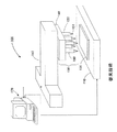
従来のマイクロアレイシステムを図1に示す。マイクロアレイシステム100は、バイオチップ120を支持するためのステージ110、XYZ位置決めシステム160に取りつけられるマイクロアレイ130、システムコントローラおよび測定データの処理に用いるコンピュータ/ワークステーション170を備えている。
(1) A conventional microarray system is shown in FIG. The
また、図2には、従来のつけペン式ナノリソグラフィ(DPN)システムを示す。DPNシステム200は、ウェーハ220を支持するステージ210、XYZ位置決めシステム260に取りつけられるマイクロペンアセンブリ230、およびシステムコントローラとして機能するコンピュータ/ワークステーション270を備えている。
FIG. 2 also shows a conventional false pen nanolithography (DPN) system. The DPN
マイクロアレイシステム100のマイクロアレイ130と同様にDPNシステム200においても、マイクロペンアセンブリ230には金属ピンが用いられている。金属ピンの製造における困難性および高コスト化は、その利用を限られたものにしている。
In the
従来の金属ピンに見られる製造上の困難性や高コスト化を招くことのないマイクロ流体導管の生産が可能であって、マイクロアレイやマイクロペンアセンブリ等のマイクロ流体素子に形成できることが必要とされている。
本発明は、設計された応力を有するばね材料フィルムを用いて形成される流体システムを提供する。 The present invention provides a fluid system formed using a spring material film having a designed stress.
上記課題を解決するための本発明の第1の態様が、基板に取り付けられた固定部と、前記基板から離れる曲がりを有するカンチレバー部とを有するばねビームを含む、流体用導管であって、前記ばねビームが、該ばねビームの前記カンチレバー部に沿って流体を運ぶための、前記カンチレバー部の前記曲がりに対して略平行に延びる第1のチャネルを定める、流体用導管により提供される。 According to a first aspect of the present invention, there is provided a fluid conduit including a spring beam having a fixed portion attached to a substrate and a cantilever portion having a bend away from the substrate, A spring beam is provided by a fluid conduit defining a first channel extending substantially parallel to the bend of the cantilever portion for carrying fluid along the cantilever portion of the spring beam.
また、本発明の第2態様が、剥離材料層の上に、該剥離材料層に対して垂直な方向の内部応力勾配を有するばね材料膜を形成する工程と、ばね材料アイランドを形成するために、前記ばね材料膜をエッチングする工程と、前記ばね材料アイランドのカンチレバー部に、前記内部応力勾配に起因する前記剥離層の第2の部分から離れる曲がりを帯びさせるために、前記剥離材料層の第1の部分を前記ばね材料アイランドの前記カンチレバー部の下から除去する工程と、前記ばねビームの前記カンチレバー部に沿って流体を運ぶための、前記カンチレバー部の前記曲がりに対して略平行に延びる第1のチャネルを定める工程と、を含む、流体用導管を形成する方法により提供される。 A second aspect of the present invention is a method for forming a spring material film having an internal stress gradient in a direction perpendicular to the release material layer on a release material layer, and forming a spring material island. Etching the spring material film; and causing the cantilever portion of the spring material island to bend away from the second portion of the release layer due to the internal stress gradient. Removing a portion of the spring material island from beneath the cantilever portion; and extending substantially parallel to the bend of the cantilever portion for carrying fluid along the cantilever portion of the spring beam. And defining a channel.
また、本発明の第3態様が、複数の流体サンプルを同時に分析するマイクロアレイシステムであって、第1のパターンに配列された複数の試験位置を含む分析用集積回路(IC)と、基板に取り付けられた固定端部と、自由端部の曲がりに対して平行に延びる第1のチャネルと、前記基板から離れる曲がりを有すると共に前記第1のチャネルから液体を分配するための分配先端部で終端する前記自由端部と、を各々が有する複数のチャネルばねプローブを含む分配アセンブリであって、前記複数のチャネルばねプローブの前記分配先端部が、前記第1のパターンと略一致する第2のパターンに配列された、分配アセンブリと、前記複数のチャネルばねプローブの各々の前記分配先端部を、前記分析用IC上の前記複数の試験位置の1つと接触するよう配置するための配置システムと、前記配置システムを制御すると共に前記分析用ICによって供給されるデータを処理するためのコンピュータ/ワークステーションと、を含むマイクロアレイシステムにより提供される。 Further, a third aspect of the present invention is a microarray system for simultaneously analyzing a plurality of fluid samples, wherein the analysis integrated circuit (IC) including a plurality of test positions arranged in a first pattern, and a microarray system attached to a substrate. A fixed channel, a first channel extending parallel to the free end bend, and a bend away from the substrate and terminating at a dispensing tip for dispensing liquid from the first channel. A dispensing assembly comprising a plurality of channel spring probes each having a free end, wherein the dispensing tip of the plurality of channel spring probes has a second pattern substantially matching the first pattern. An arrayed dispensing assembly and the dispensing tip of each of the plurality of channel spring probes are contacted with one of the plurality of test locations on the analytical IC. And deployment system for placing to be provided by microarray system comprising a computer / workstation for processing data supplied by the analyzing IC controls the placement system.
また、本発明の第4態様が、基板をパターニングするためのつけペン式ナノリソグラフィ(DPN)システムであって、基板を支持及び配置するための台と、基板に取り付けられた固定端部と、自由端部の曲がりに対して平行に延びるチャネルと、前記基板から離れる曲がりを有すると共に前記チャネルから前記基板の上に液体を分配するための分配先端部で終端する前記自由端部と、を有する第1のチャネルばねプローブを含むマイクロペンアセンブリと、前記第1のチャネルばねプローブの前記分配先端部を、前記基板と接触するよう配置すると共に、前記基板の上に所望のパターンをプリントするための配置システムと、前記配置システムを制御するためのコンピュータ/ワークステーションと、を有するDPNシステムにより提供される。 Also, a fourth aspect of the present invention is a dip pen nanolithography (DPN) system for patterning a substrate, comprising: a base for supporting and placing the substrate; a fixed end attached to the substrate; A channel extending parallel to the free end bend and the free end having a bend away from the substrate and terminating at a dispensing tip for dispensing liquid from the channel onto the substrate. A micro-pen assembly including a first channel spring probe, and the dispensing tip of the first channel spring probe arranged to contact the substrate and to print a desired pattern on the substrate. Provided by a DPN system having a deployment system and a computer / workstation for controlling the deployment system It is.
また、本発明の第5態様が、第1の面を有する第1の流体素子と、前記第1の面に取り付けられた固定部と、前記第1の面から離れる曲がりを有する自由部と、前記チャネルばねプローブの自由部に沿って流体を運ぶためのチャネルとを有するチャネルばねプローブと、を有する流体回路により提供される。 In a fifth aspect of the present invention, a first fluid element having a first surface, a fixed portion attached to the first surface, a free portion having a bend away from the first surface, A channel spring probe having a channel for carrying fluid along a free portion of the channel spring probe.
また、本発明の第6態様が、複数のプリント用先端部を有するマイクロアレイの製造方法であって、剥離材料層の上に、該剥離材料層に対して垂直な方向の内部応力勾配を有するばね材料膜を形成する工程と、複数のばね材料アイランドをアレイパターンに形成するために、前記ばね材料膜をエッチングする工程と、前記剥離材料層の第2の部分から離れる曲がりを各々が有する複数のばねビームであって、前記複数のプリント用先端部の1つを各々が構成する複数のばねビームを形成するために、前記剥離材料層の第1の部分を各前記ばね材料アイランドの前記カンチレバー部の下から除去する工程と、を含む、マイクロアレイの製造方法により提供される。 A sixth aspect of the present invention is a method for manufacturing a microarray having a plurality of printing tips, wherein a spring having an internal stress gradient on a release material layer in a direction perpendicular to the release material layer. Forming a material film; etching the spring material film to form a plurality of spring material islands in an array pattern; and forming a plurality of bends each having a bend away from a second portion of the release material layer. A spring beam, wherein a first portion of the release material layer is formed on the cantilever portion of each spring material island to form a plurality of spring beams each comprising one of the plurality of printing tips. And removing from below.
図3は、本発明の実施形態によるマイクロアレイシステム300Aの斜視図である。マイクロアレイシステム300Aは、分析用IC(analytical IC)320Aを支持するための台310Aと、配置サブシステム370Aに取り付けられた分配アセンブリ330Aと、システムコントローラ及び測定データプロセッサとして作用するコンピュータ/ワークステーション380Aとを含む。分析用IC320Aは、面ベースの分析能力を提供するバイオチップ又は他の任意のタイプのICで構成できる。配置サブシステム370Aは、コンピュータ/ワークステーション380Aによって供給された制御信号に応答して、分析用IC320A上のアレイパターンの試験溶液サンプルを収集し、及び分析用IC320A上にアレイパターンに分配するために、分配アセンブリ330Aを移動させる。配置サブシステム370Aは、分析用IC320A上に試験サンプルを分配するために必要な全ての配置操作を行うことができ、或いは、台310Aは、分析用IC320Aと分配アセンブリ330Aとを位置揃えするための付加的な配置能力を含んでもよい。試験サンプルが分配されたら、分析用IC320Aは、平行分析を行い、その結果を更に処理するためにコンピュータ/ワークステーション380Aに供給する。従って、マイクロアレイシステム300Aは、図1に示されるマイクロアレイシステム100と略同様であるが、但し、金属ピンベースのマイクロアレイ130が、チャネルばねプローブベースの分配アセンブリ330Aと置き換えられている。
FIG. 3 is a perspective view of a
分配アセンブリ330Aは、基板340A上にアレイ状に整列した複数のチャネルばねプローブ350Aを含む。上述したように、チャネルばねプローブ350Aは、マイクロアレイシステム100のプリント用先端部150よりも遙かに経済的に製造可能であり、かなり向上した精度及び設計の柔軟性を提供できる。各チャネルばねプローブ350Aは、チャネルばねプローブの曲りに平行に延びるチャネル351Aを含む。チャネル351Aは、毛管作用によって試験溶液がチャネルに沿って引かれるサイズである。任意のチャネルばねプローブ350Aが液源と接触するように配置されると、液体がチャネル351Aに引き込まれる。任意のチャネルばねプローブ350Aの先端部が分析用IC320Aの表面と接触するように配置されると、ある量の液体がチャネル351Aからバイオチップ320A上に付着する。これらの液体引込み動作と分配動作との間、液体は、毛管作用及び表面張力の力により、チャネル351A内に保持される。各チャネル351Aに沿って形成されたオプションのリザーバ352Aは、チャネルばねプローブ350Aの液体貯蔵容量を増加させることができる。各チャネルばねプローブ350Aは、先細の先端部及び単一のチャネルを有するように示されているが、本発明の実施形態によるチャネルばねプローブは、後述するように、任意の数の異なる先端部及びチャネル構成を含むことができる。例えば、チャネルばねプローブ350Aの各チャネル351Aは、分配アセンブリ330Aが分析用IC320A上に混合溶液を分配できるようにする2つのチャネルを表してもよい。
The
図4は、本発明の別の実施形態による、つけペン式ナノリソグラフィ(DPN)システム300Bの斜視図である。DPNシステム300Bは、基板320B(ウエハ等)を支持するための台310Bと、XYZ配置サブシステム370Bに取り付けられたマイクロペンアセンブリ330Bと、システムコントローラとして作用するコンピュータ/ワークステーション380Bとを含む。マイクロペンアセンブリ330Bは、取り付け台340Bに取り付けられた1つ以上のチャネルばねプローブ350Bを含む。XYZ配置サブシステム370Bは、コンピュータ/ワークステーション380Bによって供給された制御信号に応答して、ウエハ320B上に所望のパターンをプリントするために、マイクロペンアセンブリ330Bを移動させる。チャネルばねプローブ350Bの(チャネルばねプローブ350Bの曲がりに平行な)チャネル351B及びオプションのリザーバ352Bは、ウエハ320B上にプリント溶液を施すのを可能にする。従って、DPNシステム300Bは、図2に示されるDPNシステム200と略同様であるが、但し、金属ピンベースのマイクロペンアセンブリ230が、チャネルばねプローブベースのマイクロペンアセンブリ330Bと置き換えられており、ここでも、チャネルばねプローブに伴うコスト及び設計の長所を提供する。
FIG. 4 is a perspective view of a dip pen nanolithography (DPN)
図5は、本発明の別の実施形態による、流体回路300Cの概略図である。回路300Cは、微小流体の液体ブロック(microfluidic liquid volumes)を用いた又は組み込んだ任意の素子で構成可能な流体素子320C(1)及び320C(2)を含む。流体素子320C(1)及び320C(2)は、流体分析用に設計されたバイオチップ又は他の分析用集積回路(IC)で構成可能である。流体素子320C(1)は、液体の収集及び分配のためのそれぞれのチャネルばねプローブ350C(1)及び350C(2)と、面内流体経路指定用のマイクロチャネルネットワーク321Cと、流体を貯蔵するためのオプションのリザーバ322Cとを含む。チャネルばねプローブ350C(1)の自由端部が外部供給容器390C内の液体391Cと接触するように配置され、毛管作用の力によって、液体391Cの一部が、チャネルばねプローブ350C(1)の曲がりと平行に延びるチャネル351C(1)内に引き込まれる。この引き込まれた液体を、オプションのリザーバ322Cに蓄積するか、又は、マイクロチャネルネットワーク321Cへと通過させることができる。次に、マイクロチャネルネットワーク321Cは、流体素子320C(1)内の適切な場所へと、液体の経路を指定する(チャネルばねプローブ350C(2)内のチャネル351C(2)への経路指定を含む)。チャネルばねプローブ350C(2)の曲がりと平行に延びるチャネル351C(2)により、液体を、チャネルばねプローブ350C(2)の先端部から流体素子320C(2)上に分配できる。
FIG. 5 is a schematic diagram of a
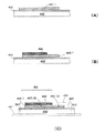
図6(A)〜図6(D)、図7(A)〜図7(C)、並びに図8(A)及び図8(B)は、本発明の別の実施形態による、図3、図4及び図5に示されているチャネルばねプローブ350A、350B及び350C等のチャネルばねプローブの製造に用いられる一般的な製造プロセスを示す、簡略化した側面断面図である。 6 (A) to 6 (D), FIGS. 7 (A) to 7 (C), and FIGS. 8 (A) and 8 (B) show FIGS. 3 and 3 according to another embodiment of the present invention. FIG. 6 is a simplified side cross-sectional view illustrating a typical manufacturing process used to manufacture channel spring probes, such as the channel spring probes 350A, 350B and 350C shown in FIGS. 4 and 5;
図6(A)を参照すると、この製造プロセスは、ウエハ440上に剥離層445を形成することから開始する。基板440は、選択された基板材料(例えば、ガラス、石英、シリコン(Si)、サファイア、酸化アルミニウム、又は適切なプラスチック)から形成される。一実施形態では、剥離層445は、基板440に付着させられたSi、窒化シリコン組成物(SiNx)、酸化シリコン組成物(SiOx)又はチタニウム(Ti)の1つ以上を含む。後述するように、剥離材料は、剥離後も、チャネルばねプローブが剥離層445の一部を介して基板440に接続されたままになるように、選択される。別の実施形態では、ばねプローブを基板440に接続するよう作用する剥離材料に隣接する分離型のアンカーパッドが別個に形成される。このように別個に形成されたアンカーパッドは、チャネルばねプローブ/基板の接続の強度を増加し得るものであるが、このようなアンカーパッドを形成すると、プロセスの工程数が増加し、それにより、プローブの総製造コストが増加する。別の実施形態では、基板440の基板材料自体が剥離層として用いられてもよい(即ち、別個の剥離材料付着プロセスは用いられず、図5のチャネルばねプローブ350C(1)及び350C(2)に示されるように、チャネルばねプローブ450が基板440に直接接続される)。
(Referring to FIG. 6A, the manufacturing process starts by forming a
図6(B)に示されるように、公知のプロセス技術を用いて、剥離層445上に、成長方向に内部応力差を含むよう設計された応力を有する(ばね材料)膜465が形成される。一実施形態では、設計された応力を有する膜465は、最下部(即ち、剥離材料層440に隣接)が上部よりも高い内部圧縮応力を有するように形成され、それにより、基板440から離れるように曲がるバイアスを生じる内部応力差が形成される。設計された応力を有する膜465にこのような内部応力差を生じる方法は、例えば、米国特許3,842,189(異なる内部応力を有する2つの金属を付着する)及び米国特許5,613,861(例えば、プロセスパラメータを変えつつ単一の金属をスパッタリングする)で教示されており、それらを参照して本明細書に援用する。一実施形態では、設計された応力を有する膜465は、ばね構造の形成に適した1つ以上の金属(例えば、モリブデン(Mo)、「モリクローム」合金(MoCr)、タングステン(W)、チタニウム−タングステン合金(Ti:W)、クロミウム(Cr)及びニッケル(Ni)の1つ以上)を含む。別の実施形態では、設計された応力を有する膜465は、Si、窒化物、酸化ケイ素、炭化物又はダイヤモンドを用いて形成される。後で更に詳しく説明するが、設計された応力を有する膜465の厚さは、幾分は、選択されたばね材料、所望のばね定数、及び最終的なばねビーム構造の形状によって決定される。
As shown in FIG. 6B, a (spring material)
図6(C)、図9(A)〜図9(D)、及び図10(A)〜図10(D)を参照すると、細長いばねマスク446(例えばフォトレジスト)が、設計された応力を有する膜465の選択された部分を覆うようにパターニングされる。ばねマスク446は、所望のチャネルばねプローブの形状に形成され、様々な先端部、チャネル及び取り付け領域の構成を含んでよい。ばねマスク446のプリントに使用可能な良好に特徴づけされたリソグラフィプロセスは、ばねマスク446の実際のジオメトリーに大きな柔軟性を可能にする。図9(A)は、本発明の一実施形態によるばねマスク446の平面図を示す。ばねマスク446は、一端部にプローブ先端部領域446−Aを含み、他端部に取り付け領域446−Bを含み、プローブ先端部領域446−Aと取り付け領域446−Bとの間にチャネル領域446−Cを含む。チャネル領域446−Cのサイズは、最終的なチャネルばねプローブに形成されて得られたチャネルが、チャネルばねプローブによって収集、貯蔵又は分配される液体に、必要な毛管作用を与えるサイズである。図9(A)は、ばねマスク446の、チャネルばねプローブが基板440から剥離される部分に対応する部分である、剥離領域446−Dを示す。
6 (C), 9 (A) -9 (D), and 10 (A) -10 (D), the elongated spring mask 446 (eg, photoresist) reduces the designed stress. The
チャネル領域446−Cはプローブ先端部領域446−Aと重なって示されているが、本発明による別の実施形態では、チャネル領域446−Cが取り付け領域446−B内に延びていてもよい。図9(B)は、剥離領域446−Dを通って取り付け領域446−B内に延びるチャネル領域446−C(1)を示している。オプションの狭い領域447は、最終的なチャネルばねプローブのために柔軟性が高い領域を設けるために含まれている(尚、狭い領域447は、説明の目的で、剥離領域446−Dと取り付け領域446−Bとが合う場所に示されているが、狭い領域447は、剥離領域446−Dに沿った任意の場所に配置可能である)。最終的なばねチャネルプローブに意図される用途に従って、チャネル領域446−Cに他の変形を行うことが可能である。例えば、図9(C)は、本発明の別の実施形態によるチャネル領域446−C(2)を示している。チャネル領域446−C(2)の内側の端部は、最終的なチャネルばねプローブのリザーバ要素を作るためのリザーバ領域520に接続されている。得られるリザーバ要素はチャネルの幅よりも広いので、チャネル領域446−C(2)の流体保持容量は増加する。リザーバ領域520は、剥離領域446−D内に配置されて示されているが、破線で示されるように、これを取り付け領域446−B内に配置することもできる。
Although channel region 446-C is shown overlapping probe tip region 446-A, in other embodiments according to the present invention, channel region 446-C may extend into mounting region 446-B. FIG. 9B shows a channel region 446-C (1) extending through the release region 446-D and into the mounting region 446-B. An optional
本発明は、チャネルばねプローブ内に複数のチャネルを形成することも可能にする。例えば、図9(D)は、本発明の別の実施形態による、チャネル領域446−C(3)及び446−C(4)を有するばねマスク446の部分を示している。図9(B)及び図9(C)に関して上述したチャネル領域と同様に、チャネル446−C(3)及び446−C(4)は、リザーバ要素を含むことができ、それに加えて/又は、破線で示されるように、取り付け領域446−B内に延びることができる。
The present invention also allows for the formation of multiple channels in a channel spring probe. For example, FIG. 9D illustrates a portion of a
これと同様の構成の柔軟性は、図9(A)に示されている取り付け領域446−B及びプローブ先端部領域446−Aにも適用される。図9(A)〜図9(D)では略長方形の領域として示されているが、取り付け領域446−Bは任意の数の形状をとることができる。図10(A)は、本発明の別の実施形態による取り付け領域446−B(1)を示す。取り付け領域446−B(1)は剥離領域446−Dと同じ幅を有し、均一な幅を有する直線状(即ち均一な幅の)チャネルばねプローブを生じる。V字型、U字型、J字型及びL字型構成を含むがこれらに限定されない、他の様々な取り付け領域構成が可能である。図10(B)は、チャネル領域446−C(5)の経路指定の拡大を可能にするために拡大された取り付け領域446−B(2)を示しており、これは、単一のリソグラフィプロセス工程による、面外流体経路指定チャネル及び面内流体経路指定チャネルの両方の形成を可能にする。 柔軟 性 A similar configuration flexibility is also applied to the mounting region 446-B and the probe tip region 446-A shown in FIG. Although shown as a substantially rectangular area in FIGS. 9A-9D, the mounting area 446-B can take any number of shapes. FIG. 10A shows a mounting area 446-B (1) according to another embodiment of the present invention. The mounting area 446-B (1) has the same width as the stripping area 446-D, resulting in a linear (ie, uniform width) channel spring probe having a uniform width. Various other mounting area configurations are possible, including but not limited to V-shaped, U-shaped, J-shaped, and L-shaped configurations. FIG. 10 (B) shows the mounting area 446-B (2) enlarged to allow for expanded routing of the channel area 446-C (5), which is a single lithographic process. The process allows for the formation of both out-of-plane and in-plane fluid routing channels.
同様に、プローブ先端部領域446−Aは、所望のチャネルばねプローブを形成するのに必要な任意の構成をとることができる。例えば、図10(C)は、本発明の別の実施形態による、プローブ先端部領域446−A(1)を示している。図9(A)の鈍いプローブ先端部領域446−Aとは対照的に、プローブ先端部領域446−A(1)は、チャネル領域446−Cの各側に先細の先端部を設ける面取り部501及び502を含む。この先細の先端部構成は、得られるチャネルばねプローブの先端部の(プリント)エッジに沿った流体の移動を減らすことができ、平たい先端部構成を有する類似のチャネルばねプローブで可能な線よりも細い流体の線を分配できるようにする。
Similarly, the probe tip region 446-A can take any configuration necessary to form the desired channel spring probe. For example, FIG. 10C shows a probe tip region 446-A (1) according to another embodiment of the present invention. In contrast to the blunt probe tip region 446-A of FIG. 9A, the probe tip region 446-A (1) has a
図10(D)は、本発明の別の実施形態による、プローブ先端部領域446−A(2)を示している。プローブ先端部領域446−A(2)は、面取り部501及び502を含むだけでなく、チャネル領域446−Cの端部を閉じる尖った先端部505も含む。尖った先端部505のサイズ及びチャネル領域446−Cの端部からの距離を適切にすると、得られるチャネルばねプローブ内の流体が、チャネル領域から尖った先端部の頂点まで運ばれ、非常に細い流体の線を分配できるようになる。本発明の実施形態によれば、チャネル領域446−Cは、尖った先端部505の頂点から1〜3μm以下の位置で終端することも可能である。
FIG. 10D illustrates a probe tip region 446-A (2) according to another embodiment of the present invention. Probe tip region 446-A (2) not only includes
チャネルばねプローブの製造プロセスに戻ると、図6(D)は、ばねアイランド465−1を形成するために、1つ以上のエッチング液480を用いてエッチングされている、ばねマスク446を囲む、設計された応力を有する膜465の露出部分を示している。なお、このエッチングプロセスは、ばね材料アイランド465−1を囲む剥離層445の限定的なエッチングが生じるように行われる。一実施形態では、設計された応力を有する膜465の露出部分を除去するために、エッチング工程は、例えば、MoCrばね金属層を除去するために硝酸セリウムアンモニウム溶液を用いるなどの、ウェットエッチングプロセスを用いて行われてもよい。別の実施形態では、設計された応力を有する膜465及び剥離層445の露出部分の上面のエッチングに、異方性ドライエッチングが用いられる。この実施形態は、例えば、Moばね金属及びSi又はTi剥離層を用いて行われてもよい。Mo、Si及びTiの全ては、反応性フッ素プラズマ中でエッチングされる。ばね材料膜をドライエッチングする長所は、それにより、より細かい形状及びより鋭い先端部を有するチャネルばねプローブを容易に得られることである。反応性プラズマ中でエッチングされない材料には、アルゴンイオンイオンミリング等の物理的イオンエッチング法により、更に異方性のエッチングを施してもよい。別の可能な実施形態では、本明細書に参照して援用するIBM J.Res.Dev.Vol.42,No.4(1998年9月4日)の655頁に記載されている電気化学的エッチングプロセスを用いて、エッチング工程を行うことができる。多くの更なるプロセスの変形及び材料の置換も可能であり、ここに与えた例に限定的な意図はない。
Returning to the channel spring probe manufacturing process, FIG. 6D illustrates a design surrounding a
図7(A)は、ばねマスク446(図6(D))が除去された後の、ばね材料アイランド465−1及び剥離層445を示している。この時点で、図7(B)に示されるように、ばね材料アイランド465−1に、オプションのチャネル領域パターニング466が形成されてもよい。チャネル領域パターニング466は、ばね材料アイランド465−1に二次的なチャネル要素を形成することを可能にする。ばね材料アイランド465−1にチャネル要素が既にパターニングされている場合は、オプションのチャネル領域パターニング466は必要ないが、それでも、ばね材料アイランド465−1に統合される要素に変形又は追加するために二次的チャネル要素を用いることもできよう。或いは、この付加的なチャネル領域パターニングを、ばね材料アイランド465−1の適切な部分が基板440から剥離された後で行うこともできる(図8(A)に関して後述する)。
FIG. 7A shows the spring material island 465-1 and the
図7(C)では、ばね材料アイランド465−1の第1の部分465−1Aの上に、剥離マスク450が形成される。剥離マスク491は、ばね材料アイランド465−1の第2の部分465−1B及びその周囲の剥離層445の部分を露出する剥離窓RWを定める。剥離マスク491は、第1の部分465−1Aを基板440に更に固定するためのストラップ構造としても作用する。本発明の一実施形態では、剥離マスク491はフォトレジストを用いて形成される。本発明の別の実施形態では、適切な金属又はエポキシを用いてもよい。本発明の別の実施形態によれば、剥離マスク491は、剥離層445及び/又はばね材料アイランド465−1の第1の部分465−1Aを適切にパターニングすることで除去されてもよい。
で は In FIG. 7C, a
この時点で、後で立ち上がる構造(即ち、図8(A)に示されているばねビーム(梁)460)の損傷を防止するために、基板440を(例えばダイシング線DL1及びDL2に沿って)ダイシングしてもよい。オプションの粘着性のダイシングテープ441を用いて、ダイシング中及びダイシング後の基板の移動を防止してもよい(即ち、ダイシングブレードは基板440(及びその上の剥離層445の部分)のみを切断し、その下の粘着テープ441は切断しない)。或いは、基板440から部分465−1Bを剥離した後にダイシングを行ってもよい。このような場合、ダイシング中に剥離されたビームを保護することが望まれる場合には、レジスト又はワックスを用いたビームのパッシべーション(不動態化)を用いてもよい。
At this point, the
図8(A)では、剥離エッチング液481(例えば、緩衝化酸化物エッチング(buffered oxide etch))を用いて、剥離層445の一部を、ばねアイランド465−1の露出部分(即ち、第2の部分465−1B)の下から選択的に除去し、湾曲したばねビーム460を形成する。露出した剥離材料を除去すると、(上述した)設計された応力を有する膜の形成中に作られた内部応力の偏差に応じて、ばねビーム460のカンチレバー部454が基板440から離れるように曲がる。ばねビーム460の固定端部453は、剥離マスク491で保護された剥離材料(支持)部445Aによって基板440に固定されたままである。或いは、剥離マスク491は、剥離後に、ばねビーム460の固定端部453から除去されてもよい。チャネル領域パターニング466が先に(例えば図7(B)において)形成されていない場合には、この時点で(即ち剥離後に)、ばねビーム460にオプションのチャネル領域パターニング466を形成してもよい。チャネル領域パターニング466が存在する場合には、図8(B)に示されている完成したチャネルばねプローブ450の実際のチャネル構造467を形成するために、追加の付着プロセス(1回又は複数回)を行ってもよい(先に述べたように、ばねビーム460の内部にチャネル要素を定めても(即ち、統合しても)よく、この場合には、ばねプローブ450にはチャネル構造467は必要ない)。
In FIG. 8A, a portion of the
チャネル構造467の形成は、図11(A)〜図11(C)に詳細に示されている。図11(A)は、図8(A)に示されている中間プローブ先端部455の正面図を示しており、チャネル領域パターニング466が、ばねビーム460の所望の部分の上に存在する。チャネル領域パターニング466は、ハードマスク(例えばハードレジスト)又は、続いて形成されるチャネル構造を除去することなく除去可能な他の任意の材料で構成可能である。図11(B)では、ばねビーム460の、チャネル領域パターニング466によってマスキングされていない部分に、チャネル構造467が形成され、チャネル領域パターニング466を除去するために、レジストストリップ(剥離剤)482が適用される。図11(C)には、得られたプローブ先端部456(図8(B)より)の正面図が示されており、以前にはチャネル領域パターニング466が占めていた隙間が、チャネル468になっている。チャネル領域パターニング466及びチャネル構造467に対しては、図13(A)〜図13(D)、図14(A)〜図14(C)、及び図15(A)に関して説明する、他の様々なジオメトリーが可能である。本発明の実施形態によれば、チャネル構造467を、ばねビーム460の上に電気めっきすることができる。本発明の別の実施形態によれば、チャネル構造467を形成するために、他の様々な材料(例えば、酸化物、窒化物、有機材料(炭化物)等)及びプロセス(例えば、スパッタリング、エバポレーション、化学蒸着(CVD)、スピニング等)を用いることができる。チャネル構造は、ばねビーム460の剥離高さを減少させ得るビーム負荷を生じるが、基板440からばねビーム460を剥離する前(即ち、図7(C)に示されているばねアイランド465−1上)に、チャネル構造(467)を形成することも可能である。
The formation of the
図8(B)に戻ると、本発明の一実施形態により、基板440は、オプション流体経路444で示されるような、一体化された流体経路を含むことが可能である。このような一体化流体経路を既に含む基板上に、チャネルばねビームを形成して、新型の流体経路指定システムの構造を簡略化することができる。例えば、更なる機械的支持及び/又は界面要素を設けるために、オプションの支持構造442を、基板440に取り付けることができる。支持構造442は、チャネルばねプローブ450に液体を供給するための、オプションの流体リザーバ443を含むことができる。このような状況では、基板440は、チャネルばねプローブ450のチャネルと支持構造442のリザーバ443とを接続する、予め形成された一体化バイア(流体経路444)を含んでもよい。流体リザーバ443は、ばねチャネルプローブ450に液体を供給するか、又は、ばねチャネルプローブ450によって集められた液体を貯蔵してもよい。
8B, in accordance with one embodiment of the present invention,
本発明の別の実施形態によれば、ばねビーム460(及びチャネル構造467)の任意の露出部を覆う、パラリン又は酸化物等のオプションの保護コーティング461(破線で示す)を形成することができる。本発明の別の実施形態によれば、FIB、EBD、カーボン−ナノチューブ成長等の方法を用いて、剥離前のばねビーム460の表面に付着させた材料をエッチングすることにより、又は、剥離後に取り付けるによって、オプションの二次的先端部469を、ばねビーム460の端部に形成する又は取り付けることができる。本明細書に参照して援用する、2002年4月30日に出願された、トーマス・ハンチェルら(Thomas Hantschel et al.)の「ばねプローブ及び作動/検出構造を有する走査プローブシステム(Scanning Probe System with Spring Probe And Actuation/Sensing Structure)」という名称の、共有の同時係属出願の米国特許出願第10/136,258号に、二次的先端部の様々な構成がより完全に記載されている。
According to another embodiment of the present invention, an optional protective coating 461 (shown in dashed lines) such as paraline or oxide can be formed over any exposed portions of spring beam 460 (and channel structure 467). . According to another embodiment of the present invention, the material deposited on the surface of the
図12(A)は、図8(B)の完成したチャネルばねプローブ450の斜視図である。このチャネルばねプローブ450は、図3に示されているマイクロアレイシステム300A、図4に示されているDPNシステム300B、及び図5に示されている流体回路300C等の任意の流体システムで使用できる。チャネルばねプローブ450は、図6(A)〜図6(D)、図7(A)〜図7(C)、並びに図8(A)及び図8(B)に関して説明したプロセスの後で又はプロセスと共に形成可能な、オプションの操作モジュール495も含む。操作モジュールは、ばねビーム460に隣接するか又は取り付けられてもよく、チャネルばねプローブ450に、アクチュエータ、ヒータ、温度センサ、応力センサ、光学検出器、偏向センサ、薬品センサ、及び(作動、信号処理等を制御するための)集積電子回路等の付加的な機能性を与えるための、様々な構造を含むことが可能である。例えば、(図3に示されているマイクロアレイ330Aや図4に示されているマイクロペンアセンブリ330B等の)チャネルばねプローブアレイ中の各チャネルばねプローブは、全てのチャネルばねプローブの先端部の位置揃えを補助するためのアクチュエータ及び偏向センサを含むことができる。
FIG. 12 (A) is a perspective view of the completed
例えば、図16(A)〜図16(C)は、それぞれ、基板940上に形成された、ばねビーム960の両側からオフセットして平行に延びる第1の細長い電極部995(A)及び第2の細長い電極部995(B)を含む作動電極構造を組み込んだ、チャネルばねプローブ950を示す平面図、側断面図、及び端面図である。細長い電極部995(A)及び995(B)の各々は、ばねビーム960の固定端部953に隣接して位置する比較的幅広の部分996と、プローブ先端部956に隣接して位置する比較的細い部分997とを含む先細の形状を有する。本発明者は、先細の電極部995(A)及び995(B)が、先細の電極設計に固有の(長さに沿った)電界強さの減少により、ばねビーム960の長さに沿って及ぼされる力を低減し、それによって、ばねビーム960の安定した「ローリング/ジッパー(rolling/zipper)」動作(図17(A)〜図17(C)を参照して後述する)を容易にすると判断した。先細の電極部995(A)及び995(B)をばねビーム960からオフセットする(即ち、ばねビーム960の両脇に取り付ける)ことにより、プローブ先端部956の完全な撓みを達成するのに必要な作動電圧が最小限になる。他の静電気作動電極パターンは、共有の同時係属出願の米国特許出願第10/136,258号に記載されている。ばねビーム960は、図16(A)に示されるような、ばねビーム960を撓ませるのに必要な力を低減するための、オプションの狭い部分947を含んでもよい。ばねビーム960は、同様の効果を与えるための、図16(B)に示されるような柔軟性が高められた部分948を含んでもよい。柔軟性が高められた部分948は、ばねビーム960を局所的に薄くすること、又はばねビーム960に局所的により軟質の材料を統合することを含む、様々な方法で形成できる。図16(A)の細い部分947及び図16(B)の柔軟性が高められた部分948は、カンチレバー部954に沿った任意の位置に配置可能である。
For example, FIGS. 16A to 16C show first elongated electrode portions 995 (A) and second elongated electrode portions 995 (A) formed on a
図17(A)〜図17(C)は、ばねビーム960の「ローリング/ジッパー」動作を示す側断面図である。図17(A)を参照すると、電圧源901によってばねビーム960及び細長い電極995(A)及び995(B)に比較的小さな電圧信号が印加されると、カンチレバー部954は実質的にそのバイアスされていない位置にとどまる(即ち、チャネルばねプローブの設計によって決定された形状に湾曲する)。図17(B)に示されるように、電圧源901によって生じる印加電圧が増加すると、カンチレバー部954は、基板940に向かうように作動されてまっすぐになり、それによってばねビーム960が「広がる」。図17(C)に示されるように、電圧源901によって生じる印加電圧が十分な大きさの値に達すると、ばねビーム960は、先端部956が基板940に当接するまで更に広がる。この作動能力は、チャネルばねプローブを組み込んだ素子の機能性を実質的に改良できる。例えば、図3に示されているマイクロアレイ330Aでは、個々のチャネルばねプローブ350Aを、基板340Aに向かうよう作動させることにより、「オフにする」ことができる。同様に、図4に示されているマイクロペンアセンブリ330Bの個々のチャネルばねプローブを、基板340Bに向かうよう(及びそこから離れるよう)作動させることにより、オフ及びオンにすることができる。
FIGS. 17 (A) to 17 (C) are side sectional views showing the “rolling / zipper” operation of the
図12(B)は、本発明者によって、上述の製造プロセスを用いて製造された、実際のチャネルばねプローブアレイ730を示す拡大写真である。チャネルばねプローブアレイ730は、基板740から離れるように湾曲したチャネルばねプローブ750(1)、750(2)、750(3)及び750(4)を含む(他にもあるが、明確にするためにここではラベルづけしない)。チャネルばねプローブ750(1)〜750(4)の各々は、固定端部753において基板740に取り付けられており、図12(A)に関して上述したように、チャネルを含む。例えば、チャネルばねプローブ750(1)は、(図10(D)に関して説明したプローブ先端部領域446−A(1)によって定められるような)先細のプローブ先端部756を貫通して延びるチャネル752を含む。図9(B)及び図9(C)に関して上述したように、チャネル752は固定端部753内へと延び、リザーバ753内で終端する。
FIG. 12B is an enlarged photograph showing an actual channel
図12(A)に戻るが、ばねビーム460内のチャネル452には、オプションのチャネル構造467のチャネル要素によって補われる又は置き換えられることも可能なチャネル452も含まれる(明確化のために、簡単に破線部分のブロックで示す)。従って、プローブ先端部456は、様々な形状をとることが可能である。例えば、図13(A)は、本発明の一実施形態によるプローブ先端部456(1)の正面図を示している。プローブ先端部456(1)は、ばねビーム460及びチャネル構造467(1)によって定められるチャネル452(1)を含む。チャネル構造部467(1)−A及び467(1)−Bは、ばねビーム部460−A及び460−Bをそれぞれ覆うように直接配置され、それにより、ばねビーム460に含まれるチャネルの高さが増加する。
12A, the
図13(B)は、本発明の別の実施形態によるプローブ先端部456(2)の正面図を示している。ばねビームの既存のチャネルに追加するのではなく、プローブ先端部456(2)のチャネル構造467(2)は、いかなるチャネル要素も含まないばねビーム460(1)(即ち、「何もない」ばねビーム)の上に形成される。従って、チャネル468(1)は、チャネル構造部467(2)−A及び467(2)−Bによって全体を定められる。 FIG. 13B shows a front view of the probe tip 456 (2) according to another embodiment of the present invention. Rather than adding to the existing channel of the spring beam, the channel structure 467 (2) of the probe tip 456 (2) includes a spring beam 460 (1) that does not include any channel elements (ie, a "blank" spring). Beam). Thus, channel 468 (1) is entirely defined by channel structures 467 (2) -A and 467 (2) -B.
図13(C)は、本発明の別の実施形態によるプローブ先端部456(3)の正面図を示している。プローブ先端部456(3)では、何もないばねビーム460(1)の上に形成されたチャネル構造467(3)は、完全に囲まれたチャネル468(2)を定める。チャネル構造467(3)は、例えば、図11(A)に示されるように、チャネル領域パターニングを完全に覆うようにめっきすることによって形成されてもよい。チャネル468(2)は全ての辺を囲まれているので、流体の出入りは、チャネル468(2)の両端部を通してのみ可能であり、流体の汚染のリスクを最小限にできると共に、チャネル468(2)内に保持された液体のより確かな輸送を提供する。 FIG. 13C shows a front view of the probe tip 456 (3) according to another embodiment of the present invention. At the probe tip 456 (3), the channel structure 467 (3) formed over the empty spring beam 460 (1) defines a completely enclosed channel 468 (2). The channel structure 467 (3) may be formed, for example, by plating so as to completely cover the channel region patterning, as shown in FIG. Because channel 468 (2) is surrounded on all sides, fluid access is only possible through the ends of channel 468 (2), minimizing the risk of fluid contamination and reducing channel 468 (2). 2) provides a more reliable transport of the liquid retained in it.
図13(D)は、本発明の別の実施形態によるプローブ先端部456(4)の正面図を示している。チャネル構造467(4)は、何もないばねビーム460(1)の上にチャネル構造部467(4)−A、467(4)−B及び467(4)−Cを配置することにより、チャネル468(3)及び468(4)を定める。この原理を用いて、チャネルばねプローブに任意の数のチャネルを形成してもよい。 FIG. 13D shows a front view of the probe tip 456 (4) according to another embodiment of the present invention. The channel structure 467 (4) is formed by placing the channel structures 467 (4) -A, 467 (4) -B and 467 (4) -C on the empty spring beam 460 (1). 468 (3) and 468 (4) are defined. Using this principle, any number of channels may be formed in the channel spring probe.
図14(A)は、本発明の別の実施形態による、複数のチャネルを含むプローブ先端部456(5)の正面図を示している。プローブ先端部456(5)は、何もないばねビーム460(1)の上面及び底面に、チャネル構造467(5)及び467(6)をそれぞれ含む。チャネル構造467(5)は、ばねビーム460(1)の上面上にチャネル468(5)を定めるチャネル構造部467(5)−A及び467(5)−Bを含み、一方、チャネル構造467(6)は、ばねビーム460(1)の底面上にチャネル468(6)を定めるチャネル構造部467(6)−A及び467(6)−Bを含む。プローブ先端部456(5)は、(チャネル構造467(5)に対して用いた破線で示唆されるように)チャネル構造467(6)のみを含んでもよく、それにより、ばねビーム460(1)の底面のみにチャネル(即ちチャネル468(6))が設けられてもよい。 FIG. 14A shows a front view of a probe tip 456 (5) including multiple channels, according to another embodiment of the present invention. Probe tip 456 (5) includes channel structures 467 (5) and 467 (6) on the top and bottom of empty spring beam 460 (1), respectively. Channel structure 467 (5) includes channel structures 467 (5) -A and 467 (5) -B that define a channel 468 (5) on the upper surface of spring beam 460 (1), while channel structure 467 (5). 6) includes channel structures 467 (6) -A and 467 (6) -B that define a channel 468 (6) on the bottom surface of the spring beam 460 (1). Probe tip 456 (5) may include only channel structure 467 (6) (as suggested by the dashed line used for channel structure 467 (5)), thereby causing spring beam 460 (1). (I.e., channel 468 (6)) may be provided only on the bottom surface of.
図14(B)は、本発明の別の実施形態による、複数の囲まれたチャネルを含むプローブ先端部456(6)の正面図を示している。プローブ先端部456(6)は、何もないばねビーム460(1)の上面及び底面に、チャネル構造467(7)及び467(8)をそれぞれ含み、それにより、完全に囲まれたチャネル468(7)及び468(8)をそれぞれ定める。プローブ先端部456(6)は、(チャネル構造467(7)に対して用いた破線で示唆されるように)チャネル構造467(8)のみを含んでもよく、それにより、ばねビーム460(1)の底面のみにチャネル(即ちチャネル468(8))が定められてもよい。 FIG. 14B illustrates a front view of a probe tip 456 (6) including a plurality of enclosed channels, according to another embodiment of the present invention. The probe tip 456 (6) includes channel structures 467 (7) and 467 (8) on the top and bottom of the empty spring beam 460 (1), respectively, thereby providing a completely enclosed channel 468 (6). 7) and 468 (8) are defined respectively. Probe tip 456 (6) may include only channel structure 467 (8) (as suggested by the dashed line used for channel structure 467 (7)), thereby causing spring beam 460 (1). (Ie, channel 468 (8)) may be defined only on the bottom surface of.
上述したタイプのチャネル構造で作られたチャネル要素は、(図9(C)及び図9(D)に関して説明したような)任意のリザーバ要素、又は、ばねビームの表面上に所望される他の構成を含むことが可能である。例えば、図14(C)は、本発明の別の実施形態による、プローブ先端部456(7)の平面図を示している。プローブ先端部456(7)は、チャネル468(9)及び横断チャネル469−A、469−B及び469−Cを定める、何もないばねビーム460(1)上に配列されたチャネル構造部467(9)−A〜467(9)−Hを含む。横断チャネル469−A、469−B及び469−Cは、チャネル468(9)に対して垂直であり、ばねビーム460(1)幅にわたって延びる。プローブ先端部468(9)が略先細の端部を有するように、チャネル構造部467(9)−A及び467(9)−Eは角度がつけられている。このような構成は、横断チャネル469−A、469−B及び469−Cが、増加した流体分配容量を提供する、例えば、穴あき(puncture)用途で使用できる。図15(A)は、プローブ先端部456(7)の側面図であり、ばねビーム460(1)の表面に沿って離間された横断チャネル469−A、469−B及び469−Cを示している。 A channel element made of a channel structure of the type described above may be used with any reservoir element (as described with respect to FIGS. 9C and 9D) or any other desired on the surface of the spring beam. Configurations can be included. For example, FIG. 14 (C) shows a plan view of a probe tip 456 (7) according to another embodiment of the present invention. The probe tip 456 (7) defines a channel 468 (9) and traversing channels 469-A, 469-B, and 469-C, defining channel structures 467 (4) arranged on an empty spring beam 460 (1). 9) -A to 467 (9) -H. Transverse channels 469-A, 469-B and 469-C are perpendicular to channel 468 (9) and extend across the width of spring beam 460 (1). Channel structures 467 (9) -A and 467 (9) -E are angled such that probe tip 468 (9) has a substantially tapered end. Such an arrangement can be used, for example, in puncture applications where the transverse channels 469-A, 469-B and 469-C provide increased fluid distribution capacity. FIG. 15A is a side view of the probe tip 456 (7), showing transverse channels 469-A, 469-B, and 469-C spaced along the surface of the spring beam 460 (1). I have.
図15(B)は、本発明の別の実施形態による、横断チャネルを有するプローブ先端部456(8)の平面図を示している。プローブ先端部456(8)は、図14(C)及び図15(A)に示されているプローブ先端部456(7)と略同様であるが、但し、プローブ先端部456(7)のチャネル構造部467(9)−A及び467(9)−Eが、尖った先端部467(9)−Jを含む単一のチャネル構造部467(9)−Iと置き換えられている。尖った先端部467(9)−Jは、プローブ先端部456(8)の端部でチャネル468(10)を閉じている。図10(D)で説明したように、尖った先端部467(9)−Jは、プローブ先端部456(8)に更なる安定性及び突き通す能力を与えつつ、依然としてチャネル468(10)への及びチャネル468(10)からの流体の輸送を可能にする。 FIG. 15B shows a plan view of a probe tip 456 (8) having a transverse channel, according to another embodiment of the present invention. The probe tip 456 (8) is substantially similar to the probe tip 456 (7) shown in FIGS. 14 (C) and 15 (A), except for the channel of the probe tip 456 (7). Structures 467 (9) -A and 467 (9) -E have been replaced with a single channel structure 467 (9) -I including a sharpened tip 467 (9) -J. Sharp tip 467 (9) -J closes channel 468 (10) at the end of probe tip 456 (8). As described in FIG. 10 (D), the pointed tip 467 (9) -J provides additional stability and penetrating ability to the probe tip 456 (8) while still providing access to the channel 468 (10). And fluid transport from channel 468 (10).
本発明を複数の実施形態と結びつけて説明したが、本発明は、開示された実施形態に限定されず、当業者には明らかな様々な変形が可能であることを理解されたい。例えば、ばねビーム(又は、Formfactor,Inc.が製造しているようなボンディングワイヤでさえ)の全ての面にめっきを施し、面外管としてのめっきのみを残してエッチングすることもできよう。従って、本発明は添付の特許請求の範囲のみによって限定される。 Although the present invention has been described in connection with a plurality of embodiments, it should be understood that the present invention is not limited to the disclosed embodiments, and that various modifications obvious to those skilled in the art are possible. For example, all surfaces of a spring beam (or even bonding wires such as those manufactured by Formfactor, Inc.) could be plated and etched leaving only the plating as an out-of-plane tube. Accordingly, the invention is not limited except as by the appended claims.
300A マイクロアレイシステム
330A 分配システム
350A チャネルばねプローブ
300B つけペン式ナノリソグラフィ(DPN)システム
330B マイクロペンアセンブリ
350B チャネルばねプローブ
380B コンピュータ/ワークステーション
300C 流体回路
320C(1) 流体素子
320C(2) 流体素子
350C(1) チャネルばねプローブ
350C(2) チャネルばねプローブ
Claims (6)
ばね材料アイランドを形成するために、前記ばね材料膜をエッチングする工程と、
前記ばね材料アイランドのカンチレバー部に、前記内部応力勾配に起因する前記剥離層の第2の部分から離れる曲がりを帯びさせるために、前記剥離材料層の第1の部分を前記ばね材料アイランドの前記カンチレバー部の下から除去する工程と、
前記ばねビームの前記カンチレバー部に沿って流体を運ぶための、前記カンチレバー部の前記曲がりに対して略平行に延びる第1のチャネルを定める工程と、
を含む、流体用導管を形成する方法。 Forming a spring material film having an internal stress gradient in a direction perpendicular to the release material layer on the release material layer;
Etching the spring material film to form a spring material island;
A first portion of the release material layer is applied to the cantilever portion of the spring material island to cause the cantilever portion of the spring material island to bend away from a second portion of the release layer due to the internal stress gradient. Removing from under the part,
Defining a first channel extending substantially parallel to the bend of the cantilever portion for carrying fluid along the cantilever portion of the spring beam;
A method of forming a fluid conduit comprising:
第1のパターンに配列された複数の試験位置を含む分析用集積回路(IC)と、
基板に取り付けられた固定端部と、自由端部の曲がりに対して平行に延びる第1のチャネルと、前記基板から離れる曲がりを有すると共に前記第1のチャネルから液体を分配するための分配先端部で終端する前記自由端部と、を各々が有する複数のチャネルばねプローブを含む分配アセンブリであって、前記複数のチャネルばねプローブの前記分配先端部が、前記第1のパターンと略一致する第2のパターンに配列された、分配アセンブリと、
前記複数のチャネルばねプローブの各々の前記分配先端部を、前記分析用IC上の前記複数の試験位置の1つと接触するよう配置するための配置システムと、
前記配置システムを制御すると共に前記分析用ICによって供給されるデータを処理するためのコンピュータ/ワークステーションと、
を含むマイクロアレイシステム。 A microarray system for simultaneously analyzing a plurality of fluid samples,
An analytical integrated circuit (IC) including a plurality of test locations arranged in a first pattern;
A fixed end attached to the substrate, a first channel extending parallel to the free end bend, and a dispensing tip having a bend away from the substrate and dispensing liquid from the first channel. A dispensing assembly comprising a plurality of channel spring probes each having a free end terminating at the dispensing end, wherein the dispensing tip of the plurality of channel spring probes substantially coincides with the first pattern. A dispensing assembly arranged in a pattern of
A positioning system for positioning the dispensing tip of each of the plurality of channel spring probes in contact with one of the plurality of test locations on the analytical IC;
A computer / workstation for controlling the placement system and processing data provided by the analysis IC;
A microarray system comprising:
基板を支持及び配置するための台と、
基板に取り付けられた固定端部と、自由端部の曲がりに対して平行に延びるチャネルと、前記基板から離れる曲がりを有すると共に前記チャネルから前記基板の上に液体を分配するための分配先端部で終端する前記自由端部と、を有する第1のチャネルばねプローブを含むマイクロペンアセンブリと、
前記第1のチャネルばねプローブの前記分配先端部を、前記基板と接触するよう配置すると共に、前記基板の上に所望のパターンをプリントするための配置システムと、
前記配置システムを制御するためのコンピュータ/ワークステーションと、
を有するDPNシステム。 A pen-based nanolithography (DPN) system for patterning a substrate, comprising:
A table for supporting and placing the substrate,
A fixed end attached to the substrate, a channel extending parallel to the free end bend, and a dispensing tip for having a bend away from the substrate and dispensing liquid from the channel onto the substrate. A micro-pen assembly including a first channel spring probe having the free end terminating;
An arrangement system for arranging the dispensing tip of the first channel spring probe in contact with the substrate and printing a desired pattern on the substrate;
A computer / workstation for controlling the deployment system;
A DPN system having:
前記第1の面に取り付けられた固定部と、前記第1の面から離れる曲がりを有する自由部と、前記チャネルばねプローブの自由部に沿って流体を運ぶためのチャネルとを有するチャネルばねプローブと、
を有する流体回路。 A first fluid element having a first surface;
A channel spring probe having a fixed portion attached to the first surface, a free portion having a bend away from the first surface, and a channel for carrying fluid along the free portion of the channel spring probe. ,
A fluid circuit having:
剥離材料層の上に、該剥離材料層に対して垂直な方向の内部応力勾配を有するばね材料膜を形成する工程と、
複数のばね材料アイランドをアレイパターンに形成するために、前記ばね材料膜をエッチングする工程と、
前記剥離材料層の第2の部分から離れる曲がりを各々が有する複数のばねビームであって、前記複数のプリント用先端部の1つを各々が構成する複数のばねビームを形成するために、前記剥離材料層の第1の部分を各前記ばね材料アイランドの前記カンチレバー部の下から除去する工程と、
を含む、マイクロアレイの製造方法。
A method of manufacturing a microarray having a plurality of printing tips,
Forming a spring material film having an internal stress gradient in a direction perpendicular to the release material layer on the release material layer;
Etching the spring material film to form a plurality of spring material islands in an array pattern;
Forming a plurality of spring beams each having a bend away from a second portion of the release material layer, the plurality of spring beams each comprising one of the plurality of printing tips. Removing a first portion of a release material layer from beneath the cantilever portion of each spring material island;
A method for producing a microarray, comprising:
Applications Claiming Priority (1)
| Application Number | Priority Date | Filing Date | Title |
|---|---|---|---|
| US10/213,059 US7241420B2 (en) | 2002-08-05 | 2002-08-05 | Capillary-channel probes for liquid pickup, transportation and dispense using stressy metal |
Publications (1)
| Publication Number | Publication Date |
|---|---|
| JP2004106172A true JP2004106172A (en) | 2004-04-08 |
Family
ID=30443701
Family Applications (1)
| Application Number | Title | Priority Date | Filing Date |
|---|---|---|---|
| JP2003286395A Pending JP2004106172A (en) | 2002-08-05 | 2003-08-05 | Fluidic conduit, method for forming fluid conduit, microarray system, dpn system, fluid circuit, and manufacturing method of microarray |
Country Status (3)
| Country | Link |
|---|---|
| US (4) | US7241420B2 (en) |
| EP (2) | EP2311567B1 (en) |
| JP (1) | JP2004106172A (en) |
Cited By (9)
| Publication number | Priority date | Publication date | Assignee | Title |
|---|---|---|---|---|
| JP2006055991A (en) * | 2004-08-20 | 2006-03-02 | Palo Alto Research Center Inc | Mems device using stressed material and shape memory material and its manufacturing method |
| JP2007535681A (en) * | 2004-04-30 | 2007-12-06 | バイオフォース・ナノサイエンシィズ・インコーポレーテッド | Method and apparatus for depositing material on a surface |
| KR100812189B1 (en) | 2007-04-24 | 2008-03-12 | 한국생산기술연구원 | Cantilever controlling by using nanofluid |
| JP2009534200A (en) * | 2006-04-19 | 2009-09-24 | ノースウエスタン ユニバーシティ | Article for parallel lithography having a two-dimensional pen array |
| JP2010527441A (en) * | 2007-05-09 | 2010-08-12 | ナノインク インコーポレーティッド | Compact nanofabrication device |
| CN101844443A (en) * | 2009-03-26 | 2010-09-29 | 精工爱普生株式会社 | Jet head, liquid-jet device and actuating device |
| WO2014188649A1 (en) * | 2013-05-23 | 2014-11-27 | パナソニックIpマネジメント株式会社 | Power generating apparatus |
| JP2015056663A (en) * | 2013-09-10 | 2015-03-23 | パロ・アルト・リサーチ・センター・インコーポレーテッドPalo Alto Research Center Incorporated | Solar cell texturing |
| JP7449876B2 (en) | 2018-11-16 | 2024-03-14 | イルミナ インコーポレイテッド | Laminated fluid circuit for fluid cartridge |
Families Citing this family (43)
| Publication number | Priority date | Publication date | Assignee | Title |
|---|---|---|---|---|
| US20030054543A1 (en) * | 1997-06-16 | 2003-03-20 | Lafferty William Michael | Device for moving a selected station of a holding plate to a predetermined location for interaction with a probe |
| US20030148539A1 (en) * | 2001-11-05 | 2003-08-07 | California Institute Of Technology | Micro fabricated fountain pen apparatus and method for ultra high density biological arrays |
| GB0128350D0 (en) | 2001-11-27 | 2002-01-16 | Lab901 Ltd | Non-rigid apparatus for microfluidic applications |
| US7241420B2 (en) | 2002-08-05 | 2007-07-10 | Palo Alto Research Center Incorporated | Capillary-channel probes for liquid pickup, transportation and dispense using stressy metal |
| US8080221B2 (en) * | 2002-08-05 | 2011-12-20 | Palo Alto Research Center Incorporated | Capillary-channel probes for liquid pickup, transportation and dispense using stressy metal |
| US8071168B2 (en) | 2002-08-26 | 2011-12-06 | Nanoink, Inc. | Micrometric direct-write methods for patterning conductive material and applications to flat panel display repair |
| AU2003287618A1 (en) * | 2002-11-12 | 2004-06-03 | Nanoink, Inc. | Methods and apparatus for ink delivery to nanolithographic probe systems |
| US20040233250A1 (en) * | 2003-03-05 | 2004-11-25 | Haushalter Robert C. | Microcontact printhead device |
| US7250139B2 (en) * | 2003-03-19 | 2007-07-31 | Northwestern University | Nanotipped device and method |
| US7217396B2 (en) | 2003-05-05 | 2007-05-15 | The Board Of Trustees Of The University Of Illinois | Microfabricated micro fluid channels |
| US20040228962A1 (en) | 2003-05-16 | 2004-11-18 | Chang Liu | Scanning probe microscopy probe and method for scanning probe contact printing |
| IL157206A0 (en) * | 2003-08-03 | 2004-02-19 | Correlating spatial position of chemical species on a substrate with molecular weight, structure and chemical reactivity | |
| US20050079711A1 (en) * | 2003-10-10 | 2005-04-14 | Cabot Microelectronics Corp. | Hollow tip array with nanometer size openings and formation thereof |
| CA2543091C (en) * | 2003-10-24 | 2013-09-03 | John Austin | Apparatus and method for dispensing fluid, semi-solid and solid samples |
| CA2557472C (en) * | 2004-02-25 | 2013-05-07 | Nanoink, Inc. | Micrometric direct-write methods for patterning conductive material and applications to flat panel display repair |
| EP2705792B1 (en) | 2004-03-06 | 2015-04-15 | F. Hoffmann-La Roche AG | Body fluid sampling device |
| US7819822B2 (en) * | 2004-03-06 | 2010-10-26 | Roche Diagnostics Operations, Inc. | Body fluid sampling device |
| US7775087B2 (en) * | 2004-03-16 | 2010-08-17 | Northwestern University | Microchannel forming method and nanotipped dispensing device having a microchannel |
| US20050236566A1 (en) * | 2004-04-26 | 2005-10-27 | Chang Liu | Scanning probe microscope probe with integrated capillary channel |
| JP4988569B2 (en) * | 2004-07-23 | 2012-08-01 | エイエフエイ・コントロールズ,リミテッド・ライアビリティ・カンパニー | Microvalve assembly and related method |
| DE102004050466A1 (en) * | 2004-10-16 | 2006-04-20 | Olympus Diagnostica Lab Automation Gmbh | Device for pipetting |
| EP1658897A1 (en) * | 2004-11-22 | 2006-05-24 | Roche Diagnostics GmbH | Bent microfluidic device |
| GB0502556D0 (en) * | 2005-02-08 | 2005-03-16 | Lab901 Ltd | Analysis instrument |
| US20080279727A1 (en) * | 2005-03-01 | 2008-11-13 | Haushalter Robert C | Polymeric Fluid Transfer and Printing Devices |
| CN100578228C (en) * | 2005-09-09 | 2010-01-06 | 博奥生物有限公司 | Minute quantity liquid precise distribution instrument and using method thereof |
| US7281419B2 (en) | 2005-09-21 | 2007-10-16 | The Board Of Trustees Of The University Of Illinois | Multifunctional probe array system |
| US20090093735A1 (en) * | 2006-03-29 | 2009-04-09 | Stephan Korner | Test unit and test system for analyzing body fluids |
| US8192794B2 (en) | 2006-04-19 | 2012-06-05 | Northwestern University | Massively parallel lithography with two-dimensional pen arrays |
| CN100405539C (en) * | 2006-07-27 | 2008-07-23 | 华中科技大学 | Micro-thin pen for direct writing electronical photoelectronic component and its constituting device |
| US8252160B2 (en) * | 2006-07-28 | 2012-08-28 | Hewlett-Packard Development Company, L.P. | Prevention of fluid delivered to reservoir from wicking into channels within microfluidic device |
| GB2445739A (en) | 2007-01-16 | 2008-07-23 | Lab901 Ltd | Polymeric laminates containing heat seals |
| CA2714005A1 (en) * | 2008-02-05 | 2009-08-13 | Nanoink, Inc. | Array and cantilever array leveling |
| US8393785B2 (en) * | 2009-05-14 | 2013-03-12 | Palo Alto Research Center Incorporated | Nanocalorimeter based on thermal probes |
| US8130072B2 (en) * | 2009-05-14 | 2012-03-06 | Palo Alto Research Center Incorporated | Vanadium oxide thermal microprobes |
| US8579414B2 (en) | 2009-12-23 | 2013-11-12 | Xerox Corporation | Self-assembling structures for electrostatic extraction of pigments from liquid inks for marking |
| CN102270257B (en) * | 2011-06-30 | 2013-02-06 | 南京开瑞汽车技术有限公司 | Method for designing and calculating fluid passage |
| EP2825314A1 (en) * | 2012-03-16 | 2015-01-21 | Life Technologies Corporation | Systems and methods for biological analysis |
| CN102718182B (en) * | 2012-07-10 | 2015-05-20 | 西南交通大学 | Large-area-friction-induced micron-scale processing equipment in multipoint contact mode |
| US10082500B2 (en) | 2013-08-22 | 2018-09-25 | Franz Baudenbacher | Device and method for detecting a target analyte |
| US9815261B2 (en) * | 2013-09-25 | 2017-11-14 | GM Global Technology Operations LLC | Applications of a reversible dry adhesive system |
| CA3010974A1 (en) | 2016-01-11 | 2017-07-20 | Verndari, Inc. | Microneedle compositions and methods of using same |
| CN109862936B (en) * | 2016-08-03 | 2023-06-27 | 沃达瑞公司 | Microarray and method |
| CN111747375B (en) * | 2020-07-08 | 2023-08-11 | 河南大学 | Method for regulating and controlling electrical property and photoelectric output of p-Si/n-ZnO thin film heterojunction |
Family Cites Families (21)
| Publication number | Priority date | Publication date | Assignee | Title |
|---|---|---|---|---|
| US3842189A (en) * | 1973-01-08 | 1974-10-15 | Rca Corp | Contact array and method of making the same |
| US5063081A (en) * | 1988-11-14 | 1991-11-05 | I-Stat Corporation | Method of manufacturing a plurality of uniform microfabricated sensing devices having an immobilized ligand receptor |
| WO1991012949A1 (en) * | 1990-02-20 | 1991-09-05 | The Procter & Gamble Company | Open capillary channel structures, improved process for making capillary channel structures, and extrusion die for use therein |
| JPH07103996A (en) | 1993-10-06 | 1995-04-21 | Oki Electric Ind Co Ltd | Gas flow sensor and method for forming the same |
| DE4437260C1 (en) * | 1994-10-18 | 1995-10-19 | Siemens Ag | Micro-mechanical electrostatic relay with slotted spring tongue surface |
| US5613861A (en) * | 1995-06-07 | 1997-03-25 | Xerox Corporation | Photolithographically patterned spring contact |
| KR0185329B1 (en) * | 1996-03-27 | 1999-05-15 | 이형도 | Recording method using motor inertia of recording liquid |
| ATE218194T1 (en) | 1996-12-11 | 2002-06-15 | Gesim Ges Fuer Silizium Mikros | MICROEJECTION PUMP |
| US6396966B1 (en) * | 1997-02-09 | 2002-05-28 | Nanoptics, Inc. | Glass structures for nanodelivery and nanosensing |
| US6101946A (en) * | 1997-11-21 | 2000-08-15 | Telechem International Inc. | Microarray printing device including printing pins with flat tips and exterior channel and method of manufacture |
| US6159368A (en) * | 1998-10-29 | 2000-12-12 | The Perkin-Elmer Corporation | Multi-well microfiltration apparatus |
| US6827979B2 (en) * | 1999-01-07 | 2004-12-07 | Northwestern University | Methods utilizing scanning probe microscope tips and products therefor or produced thereby |
| US6888362B2 (en) * | 2000-11-09 | 2005-05-03 | Formfactor, Inc. | Test head assembly for electronic components with plurality of contoured microelectronic spring contacts |
| AU2573801A (en) | 1999-11-02 | 2001-05-14 | University Of Hawaii | Method for fabricating arrays of micro-needles |
| US6213789B1 (en) * | 1999-12-15 | 2001-04-10 | Xerox Corporation | Method and apparatus for interconnecting devices using an adhesive |
| JP3650722B2 (en) | 2000-05-18 | 2005-05-25 | 株式会社アドバンテスト | Probe card and manufacturing method thereof |
| US6766817B2 (en) * | 2001-07-25 | 2004-07-27 | Tubarc Technologies, Llc | Fluid conduction utilizing a reversible unsaturated siphon with tubarc porosity action |
| AU2003211027A1 (en) * | 2002-03-27 | 2003-10-13 | Nanoink, Inc. | Method and apparatus for aligning patterns on a substrate |
| US6668628B2 (en) * | 2002-03-29 | 2003-12-30 | Xerox Corporation | Scanning probe system with spring probe |
| FR2839662B1 (en) | 2002-05-16 | 2005-12-02 | Centre Nat Rech Scient | DEVICE FOR LOCALLY DEPOSITING AT LEAST ONE BIOLOGICAL SOLUTION |
| US7241420B2 (en) * | 2002-08-05 | 2007-07-10 | Palo Alto Research Center Incorporated | Capillary-channel probes for liquid pickup, transportation and dispense using stressy metal |
-
2002
- 2002-08-05 US US10/213,059 patent/US7241420B2/en not_active Expired - Fee Related
-
2003
- 2003-07-28 EP EP10181968.8A patent/EP2311567B1/en not_active Expired - Lifetime
- 2003-07-28 EP EP20030254696 patent/EP1388369B1/en not_active Expired - Fee Related
- 2003-08-05 JP JP2003286395A patent/JP2004106172A/en active Pending
-
2005
- 2005-11-03 US US11/267,762 patent/US7749448B2/en active Active
-
2009
- 2009-04-22 US US12/428,397 patent/US8241509B2/en active Active
-
2010
- 2010-05-06 US US12/775,452 patent/US8287744B2/en not_active Expired - Fee Related
Cited By (9)
| Publication number | Priority date | Publication date | Assignee | Title |
|---|---|---|---|---|
| JP2007535681A (en) * | 2004-04-30 | 2007-12-06 | バイオフォース・ナノサイエンシィズ・インコーポレーテッド | Method and apparatus for depositing material on a surface |
| JP2006055991A (en) * | 2004-08-20 | 2006-03-02 | Palo Alto Research Center Inc | Mems device using stressed material and shape memory material and its manufacturing method |
| JP2009534200A (en) * | 2006-04-19 | 2009-09-24 | ノースウエスタン ユニバーシティ | Article for parallel lithography having a two-dimensional pen array |
| KR100812189B1 (en) | 2007-04-24 | 2008-03-12 | 한국생산기술연구원 | Cantilever controlling by using nanofluid |
| JP2010527441A (en) * | 2007-05-09 | 2010-08-12 | ナノインク インコーポレーティッド | Compact nanofabrication device |
| CN101844443A (en) * | 2009-03-26 | 2010-09-29 | 精工爱普生株式会社 | Jet head, liquid-jet device and actuating device |
| WO2014188649A1 (en) * | 2013-05-23 | 2014-11-27 | パナソニックIpマネジメント株式会社 | Power generating apparatus |
| JP2015056663A (en) * | 2013-09-10 | 2015-03-23 | パロ・アルト・リサーチ・センター・インコーポレーテッドPalo Alto Research Center Incorporated | Solar cell texturing |
| JP7449876B2 (en) | 2018-11-16 | 2024-03-14 | イルミナ インコーポレイテッド | Laminated fluid circuit for fluid cartridge |
Also Published As
| Publication number | Publication date |
|---|---|
| EP2311567B1 (en) | 2013-05-08 |
| US8287744B2 (en) | 2012-10-16 |
| EP1388369A2 (en) | 2004-02-11 |
| EP1388369A3 (en) | 2004-12-29 |
| US7241420B2 (en) | 2007-07-10 |
| EP2311567A1 (en) | 2011-04-20 |
| US20040022681A1 (en) | 2004-02-05 |
| US7749448B2 (en) | 2010-07-06 |
| EP1388369B1 (en) | 2015-04-29 |
| US20060057031A1 (en) | 2006-03-16 |
| US20090233815A1 (en) | 2009-09-17 |
| US20100213161A1 (en) | 2010-08-26 |
| US8241509B2 (en) | 2012-08-14 |
Similar Documents
| Publication | Publication Date | Title |
|---|---|---|
| JP2004106172A (en) | Fluidic conduit, method for forming fluid conduit, microarray system, dpn system, fluid circuit, and manufacturing method of microarray | |
| US6642129B2 (en) | Parallel, individually addressable probes for nanolithography | |
| US7523650B2 (en) | Multifunctional probe array system | |
| US6668628B2 (en) | Scanning probe system with spring probe | |
| EP1698905B9 (en) | Nano-drive for high resolution positioning and for positioning of a multi-point probe | |
| US8080221B2 (en) | Capillary-channel probes for liquid pickup, transportation and dispense using stressy metal | |
| US8261662B1 (en) | Active pen nanolithography | |
| US20110163061A1 (en) | Method Of Producing Microsprings Having Nanowire Tip Structures | |
| US20080230856A1 (en) | Intermediate probe structures for atomic force microscopy | |
| EP2535725A1 (en) | A probe for scanning probe microscopy | |
| EP1544865B1 (en) | A method for making probes for atomic force microscopy | |
| US10384230B2 (en) | Method for producing a substrate structured by nanowires, produced substrate, and use of the substrate |
Legal Events
| Date | Code | Title | Description |
|---|---|---|---|
| A621 | Written request for application examination |
Free format text: JAPANESE INTERMEDIATE CODE: A621 Effective date: 20060727 |
|
| A977 | Report on retrieval |
Free format text: JAPANESE INTERMEDIATE CODE: A971007 Effective date: 20081211 |
|
| A131 | Notification of reasons for refusal |
Free format text: JAPANESE INTERMEDIATE CODE: A131 Effective date: 20090120 |
|
| A601 | Written request for extension of time |
Free format text: JAPANESE INTERMEDIATE CODE: A601 Effective date: 20090417 |
|
| A521 | Request for written amendment filed |
Free format text: JAPANESE INTERMEDIATE CODE: A523 Effective date: 20090422 |
|
| A602 | Written permission of extension of time |
Free format text: JAPANESE INTERMEDIATE CODE: A602 Effective date: 20090422 |
|
| A02 | Decision of refusal |
Free format text: JAPANESE INTERMEDIATE CODE: A02 Effective date: 20090901 |