US7775087B2 - Microchannel forming method and nanotipped dispensing device having a microchannel - Google Patents
Microchannel forming method and nanotipped dispensing device having a microchannel Download PDFInfo
- Publication number
- US7775087B2 US7775087B2 US11/516,039 US51603906A US7775087B2 US 7775087 B2 US7775087 B2 US 7775087B2 US 51603906 A US51603906 A US 51603906A US 7775087 B2 US7775087 B2 US 7775087B2
- Authority
- US
- United States
- Prior art keywords
- thin film
- microchannel
- microcantilever
- thin films
- cantilever
- Prior art date
- Legal status (The legal status is an assumption and is not a legal conclusion. Google has not performed a legal analysis and makes no representation as to the accuracy of the status listed.)
- Expired - Fee Related, expires
Links
Images


Classifications
-
- B—PERFORMING OPERATIONS; TRANSPORTING
- B81—MICROSTRUCTURAL TECHNOLOGY
- B81C—PROCESSES OR APPARATUS SPECIALLY ADAPTED FOR THE MANUFACTURE OR TREATMENT OF MICROSTRUCTURAL DEVICES OR SYSTEMS
- B81C1/00—Manufacture or treatment of devices or systems in or on a substrate
- B81C1/00015—Manufacture or treatment of devices or systems in or on a substrate for manufacturing microsystems
- B81C1/00023—Manufacture or treatment of devices or systems in or on a substrate for manufacturing microsystems without movable or flexible elements
- B81C1/00055—Grooves
- B81C1/00071—Channels
-
- B—PERFORMING OPERATIONS; TRANSPORTING
- B82—NANOTECHNOLOGY
- B82Y—SPECIFIC USES OR APPLICATIONS OF NANOSTRUCTURES; MEASUREMENT OR ANALYSIS OF NANOSTRUCTURES; MANUFACTURE OR TREATMENT OF NANOSTRUCTURES
- B82Y10/00—Nanotechnology for information processing, storage or transmission, e.g. quantum computing or single electron logic
-
- B—PERFORMING OPERATIONS; TRANSPORTING
- B82—NANOTECHNOLOGY
- B82Y—SPECIFIC USES OR APPLICATIONS OF NANOSTRUCTURES; MEASUREMENT OR ANALYSIS OF NANOSTRUCTURES; MANUFACTURE OR TREATMENT OF NANOSTRUCTURES
- B82Y40/00—Manufacture or treatment of nanostructures
-
- G—PHYSICS
- G03—PHOTOGRAPHY; CINEMATOGRAPHY; ANALOGOUS TECHNIQUES USING WAVES OTHER THAN OPTICAL WAVES; ELECTROGRAPHY; HOLOGRAPHY
- G03F—PHOTOMECHANICAL PRODUCTION OF TEXTURED OR PATTERNED SURFACES, e.g. FOR PRINTING, FOR PROCESSING OF SEMICONDUCTOR DEVICES; MATERIALS THEREFOR; ORIGINALS THEREFOR; APPARATUS SPECIALLY ADAPTED THEREFOR
- G03F7/00—Photomechanical, e.g. photolithographic, production of textured or patterned surfaces, e.g. printing surfaces; Materials therefor, e.g. comprising photoresists; Apparatus specially adapted therefor
- G03F7/0002—Lithographic processes using patterning methods other than those involving the exposure to radiation, e.g. by stamping
-
- B—PERFORMING OPERATIONS; TRANSPORTING
- B81—MICROSTRUCTURAL TECHNOLOGY
- B81B—MICROSTRUCTURAL DEVICES OR SYSTEMS, e.g. MICROMECHANICAL DEVICES
- B81B2201/00—Specific applications of microelectromechanical systems
- B81B2201/05—Microfluidics
- B81B2201/058—Microfluidics not provided for in B81B2201/051 - B81B2201/054
-
- G—PHYSICS
- G01—MEASURING; TESTING
- G01Q—SCANNING-PROBE TECHNIQUES OR APPARATUS; APPLICATIONS OF SCANNING-PROBE TECHNIQUES, e.g. SCANNING PROBE MICROSCOPY [SPM]
- G01Q80/00—Applications, other than SPM, of scanning-probe techniques
-
- Y—GENERAL TAGGING OF NEW TECHNOLOGICAL DEVELOPMENTS; GENERAL TAGGING OF CROSS-SECTIONAL TECHNOLOGIES SPANNING OVER SEVERAL SECTIONS OF THE IPC; TECHNICAL SUBJECTS COVERED BY FORMER USPC CROSS-REFERENCE ART COLLECTIONS [XRACs] AND DIGESTS
- Y10—TECHNICAL SUBJECTS COVERED BY FORMER USPC
- Y10T—TECHNICAL SUBJECTS COVERED BY FORMER US CLASSIFICATION
- Y10T29/00—Metal working
- Y10T29/42—Piezoelectric device making
Definitions
- the present invention relates to a method of forming an elongated microchannel as well as to a thin film structure and microcantilever having a microchannel for use in a dispensing device wherein fluid material is supplied via the microchannel to the microtip.
- DPN Dip-pen nanolithography
- AFM atomic force microscope
- DPN is disadvantageous in that repeated re-inking of the dispensing tip is required to replenish molecules when large surface areas are to be patterned or when complex patterns are required. DPN also suffers from low speed and throughput due to its serial nature and limited scan size.
- micropipette used as an AFM probe as described in Appl/Phys. Lett. 65 (5), 648 (1994).
- the micropipette technique suffers from the disadvantage of irregular shape of the micropipette, low reproducibility, and low resolution.
- the micropipette is difficult to integrate in array format to carry out massive pattering operations on one or more substrates.
- millipede:parallel read/write is described in IEEE Trans. on Nanotech. 1 (1), 39 (2002) and involves a cantilevered AFM probe having a heated tip able to write on a thermoplastic substrate by embossing the tip into the thermoplastic material.
- the technique does not dispense any material, but is illustrative for a massively parallel writing method using AFM probe arrays.
- the present invention provides a thin film structure and method of forming a microchannel in a manner that does not require edge sealing along its length, improves sealing capability, simplifies processing steps, and provides other advantages.
- the present invention provides a method of forming a microchannel comprising the steps of forming a first thin film on a side of a substrate, forming a fugitive second thin film on the first thin film such that the second thin film defines a precursor of the elongated microchannel and a plurality of extensions connected to and extending transversely relative to the precursor along a length thereof.
- a third thin film is formed on the first thin film and the fugitive second thin film such that the second thin film resides between the first thin film and the third thin film.
- a respective access site is formed in a region of the third thin film residing on a respective extension and penetrating to the fugitive second thin film.
- the fugitive second thin film forming the precursor is selectively removed from between the first thin film and the third thin film using an etching medium introduced through the access sites, thereby forming the microchannel between the first thin film and the third thin film.
- the method preferably further includes forming a sealing layer on the third thin film in a manner to close off open access sites remaining after selective removal of the second thin film.
- the method also includes forming the first thin film, second thin film, and third thin film on a pointed microtip of the substrate, providing an access site in the third thin film at the microtip and selectively removing the fugitive second layer at the tip using an etching medium introduced through the access site to form an annular microchannel disposed between the first thin film and the third thin film at the microtip and communicated to the channel void.
- the first thin film may comprise silicon nitride, diamond, silicon carbide or other suitable material.
- the method includes leaving some of the fugitive second thin film at the extensions after selective removal of the precursor.
- the first film is formed to define an elongated cantilever of a dispensing device such that the microchannel extends along a length of the cantilever.
- the method preferably further includes forming a reservoir on an opposite side of the substrate from the first thin film wherein the reservoir communicates via the microchannel with the microtip to dispense material from the reservoir to the microtip where the material is dispensed onto a surface.
- the method further includes forming a piezoelectric actuator layer on the cantilever.
- the actuator layer is formed on the sealing layer that seals the access site(s).
- the actuator layer is formed on the sealing layer and then the actuator layer and sealing layer are patterned to overlie the cantilever.
- the present invention envisions a thin film structure comprising a first thin film and second thin film forming a microchannel therebetween.
- the microchannel includes a plurality of microchannel extensions that extend transversely therefrom along its length, one or both of the first thin film or second thin film having a respective access site to a respective extension of the microchannel to provide access thereto.
- a sealing material is provided to close off the access site(s).
- the sealing material preferably comprises a sealing layer on one of the first thin film or second thin film.
- the extensions of the microchannel of the thin film structure can contain material of a thin film formerly residing between the first thin film and the second thin film at the microchannel.
- the present invention further envisions a microcantilever comprising a pair of thin films and having a microchannel along its length formed between the thin films, the microchannel having a plurality of microchannel extensions that extend transversely therefrom along its length, and respective access sites in one of the thin films providing access to respective extensions of the microchannel, and a sealing material closing off the access sites.
- the microcantilever further includes a microtip for dispensing material.
- the microtip preferably includes an annular microchannel formed about a pointed tip.
- the pointed tip is formed by one of a pair of thin films and the annular microchannel is formed between the pair of thin films about the pointed tip.
- the pointed tip can comprise silicon nitride, diamond, silicon carbide or other hard material.
- the microcantilever can be formed to extend from a semiconductor chip substrate.
- the microcantilever can include a piezoelectric actuator layer on one of the first thin film or second thin film to enable control of the cantilever microtip position and motion during material dispensing, such as during writing or probing.
- the microcantilever preferably further includes a reservoir on an opposite side of the cantilever from the microtip.
- One of the thin films includes one or more openings at such a location that the one or more openings communicate to the reservoir.
- FIG. 1 is a schematic view of an atomic force microscope (AFM) head having a holder on which an illustrative writing material dispensing device shown schematically mounted thereon for writing on a surface.
- AFM atomic force microscope
- FIG. 2 is a schematic perspective view of a dispensing device pursuant to an illustrative embodiment of the invention for dispensing material onto a surface.
- FIG. 2A is a reflected light, top side view photograph of a chip having twin arrays of 12 equal-length cantilevers and multiple reservoirs.
- FIG. 2B is a scanning electron micrograph of one of the cantilevers showing the microtip at an end thereof and the sealing layer overlying the microchannel-forming thin films.
- FIG. 2C is a scanning electron micrograph of the microtip.
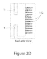
- FIG. 2D is a reflected light, backside top view photograph of a chip having twin arrays of 12 equal-length cantilevers and multiple reservoirs.
- FIGS. 3A , 3 B, and 3 C are plan views of formation of first, second and third thin films to form a cantilever on a semiconductor chip substrate.
- the third (top) film is shown as transparent to reveal the second film therebelow.
- FIGS. 4A through 4H are transverse sectional view of the first, second, and third thin films deposited to form the cantilever on the chip substrate with FIG. 4B being a transverse sectional view through FIG. 3A , FIG. 4C being a transverse sectional view through FIG. 3B , and FIG. 4E being a transverse sectional view through FIG. 3C .
- FIG. 5 is a optical micrograph at 533 ⁇ of the microchannel and microchannel extensions after selective etching of the fugitive second thin film with some of the fugitive (sacrificial) second thin film remaining in the microchannel extensions.
- FIG. 6 is an optical micrograph at 200 ⁇ showing cantilevers with microchannel precursors thereof connected to microchannel precursors on the chip substrate.
- FIGS. 7A through 7I illustrate a microfabrication method according to an embodiment of the invention to make the reservoirs.
- FIG. 8 is a plan view of a lower Pt electrode pattern.
- an atomic force microscope (AFM) scanning head 10 having a tip carrier 12 is illustrated schematically for purposes of illustration and not limitation.
- a dispensing device 100 having a cantilever 102 with a microtip 106 pursuant to an illustrative embodiment of the invention is schematically shown disposed or mounted on the tip carrier 12 for movement (e.g. raster scanning) with the scanning head 10 to dispense writing material M on a surface S.
- a silicon semiconductor chip having the dispensing device 100 fabricated thereon is mounted on the tip carrier 12 in the same manner as a conventional AFM probe tip such that the AFM hardware and software can be used to move the dispensing device to write a pattern with nanometer resolution of pattern features on surface S.
- a dispensing device 100 pursuant to an illustrative embodiment of the invention is shown for purposes of illustration and not limitation.
- the present invention can be practiced to form a microchannel in a thin film structure for any use or purpose and is not limited to a microchannel for a dispensing device.
- the dispensing device 100 is shown schematically as comprising a semiconductor chip substrate C on which the dispensing device is fabricated by micromachining techniques as described below.
- the dispensing device 100 comprises one or more elongated cantilevers 102 (six cantilevers shown) that each comprise a plurality of thin films arranged relative to one another as described below to define an elongated cantilever body having a microchannel 104 , FIG. 4H , therein and to define a material-dispensing working microtip 106 proximate an end of each cantilever remote from the chip substrate C.
- Each microtip 106 is communicated to a respective microchannel 104 to receive material M therefrom to be dispensed from the microtip onto the surface S.
- the microchannels of cantilevers 102 a , 102 b , 102 c are communicated to a material-containing reservoir 110 that supplies material M to the microchannels.
- the microchannels of cantilevers 102 a ′, 102 b ′, 102 c ′ are communicated to a different common material-containing reservoir 110 that supplies the same or different material M to the microchannels.
- Each microchannel may be communicated to its own respective material-containing reservoir, however.
- the microcantilevers 102 each can include a piezoelectric actuator layer PZT and its two electrical contact layers (not shown in FIG. 2 ) to enable control of the cantilever microtip position and motion during material dispensing, such as during writing or probing.
- the PZT layer is used with a platinum or other electrode (50-100 nm thick) underneath it and a similar electrode on top of it to provide electrical contacts.
- a chromium or titanium adhesion layer (5-10 nm thick) is provided between the platinum electrode and the sealing layer to be described.
- FIGS. 2A and 2B illustrate an actual dispensing device fabricated on a silicon chip substrate wherein the device includes twin arrays of twelve equal-length cantilevers 102 on opposite sides of the chip substrate C and multiple fluid material reservoirs 110 connected by a respective microchannel 105 to a respective microchannel 104 of each cantilever 102 .
- FIG. 2B illustrates one of the cantilevers showing the microchannels 104 communicated in fluid flow relation to an annular space about the microtip 106 and a sealing layer 18 described below overlying a portion of the cantilever.
- the microtip 106 is shown in greater detail in FIG.
- the fluid dispensing microtips 106 are formed in a manner described in U.S. Pat. No. 7,250,139, the teachings of which are incorporated herein by reference.
- FIGS. 3A , 3 B, and 3 C and FIGS. 4A through 4H the formation of one of the cantilevers 102 on the chip (wafer) C is shown for a particular illustrative embodiment of the invention. However, this is offered for purposes of illustration and not limitation since all six (or particular number) of the cantilevers 102 will be formed simultaneously on the chip C using this methodology.
- a first thin film 10 is shown deposited on the silicon chip substrate C.
- the first thin film 10 can comprise silicon nitride (Si 3 N 4 ) having a thickness of 0.350-0.500 microns and can be deposited by LPCVD (low pressure chemical vapor deposition) or PECVD (plasma enhanced chemical vapor deposition).
- the first thin film 10 can comprises a form of diamond (e.g. nanocrystalline diamond) or silicon carbide to provide a hard film at the microtip 106 region of the cantilever.
- the first thin film 10 is patterned by conventional lithography to define a cantilever precursor shape shown in FIGS. 3A and 4B .
- the cantilever shape can have any suitable dimensions for an intended application.
- cantilever lengths can be from 300 microns to 500 microns with cantilever stiffness of 0.05 to 0.4 N/m for purposes of illustration and not limitation.
- the lithographic patterning can be conducted using a conventional photoresist layer and etching medium such as CF 4 reactive ion etching (RIE) for a silicon nitride thin film.
- RIE reactive ion etching
- a second thin film 12 is shown deposited on the cantilever-patterned first thin film 10 .
- the second thin film 12 can comprise silicon dioxide (SiO 2 ) or boron-phosphorous silicon glass (BPSG) having a thickness of 0.3-0.6 microns and can be deposited by LPCVD or PECVD.
- the second thin film 12 is patterned by conventional lithographic techniques to define the precursor P of the elongated microchannel 104 and a plurality of microchannel precursor extensions or beams PE connected to and extending transversely relative to the precursor P along the length of the precursor as shown in FIG. 3B and FIG. 4C .
- the microchannel precursors P can have a width of four to seven microns and height of 0.3 to 0.6 microns and the extensions or beams PE can have a width of one to three microns and various lengths for purposes of illustration and not limitation.
- a third thin film 14 is shown deposited on the first thin film 10 and second thin film 12 (precursor 12 ) on the chip substrate C.
- the third thin film 14 can comprise silicon nitride (Si 3 N 4 ) having a thickness of 0.5-1 micron and can be deposited by LPCVD for purposes of illustration and not limitation.
- the third thin film 14 is patterned by conventional lithographic techniques to define the shape of the cantilever (or at least to cover the precursor P and extensions PE) and also to form holes, passages or other access sites 20 in a region of the third thin film 14 residing on a respective extension PE and penetrating to the fugitive second thin film 12 .
- the access sites 20 provide entry or access of an etching medium in the next step to selectively remove the second thin film 12 .
- the third thin film 14 is patterned by conventional lithography using a conventional photoresist layer and etching medium such as CF 4 reactive ion etching (RIE).
- RIE reactive ion etching
- the access sites 20 can have any suitable shape, such as oval as shown, circular or any other shape, and dimensions to permit etching medium to penetrate to the second thin film 12 .
- the oval access sites 20 shown can have a major dimension of three-five microns and a minor dimension of two-three microns.
- the extensions PE and access sites 20 are provided at locations and distances along the microchannel precursor P, FIG. 3C , in a manner to provide relatively uniform removal (etching) of the second thin film 12 along the length of the precursor P within desired etching times.
- the fugitive second thin film 12 forming the precursor P is selectively removed from between the first thin film 10 and the third thin film 14 using an etching medium introduced through the access sites 20 , thereby forming the microchannel 104 between the first thin film 10 and the third thin film 14 as shown in FIG. 4F .
- Selective etching of the fugitive second thin film 12 is conducted by a buffered oxide etch (hydrofluoric acid+ammonium fluoride 1:10).
- the microchannels in the cantilevers 102 can have any suitable dimensions such as a width of four to seven microns and height of 0.3 to 0.6 microns for purposes of illustration and not limitation.
- the microchannel extensions 104 e can have a width of one to three microns and various lengths transverse to the microchannel, the lengths typically being greater than three microns for purposes of illustration and not limitation.
- FIG. 5 illustrates an actual microchannel 104 formed after selective removal of the fugitive second thin film 12 from between the first and third thin films 10 , 14 by etching as described above.
- FIG. 5 reveals that some of the fugitive second thin film is still present in the extensions or beams PE after selective etching of the second thin film and can impart increased lateral bending and torsional stiffness to the cantilever 102 .
- a sealing layer 18 is shown deposited on the third thin film 14 in a manner to seal the access sites 20 in the third thin film layer.
- the sealing layer 18 can comprise silicon dioxide (SiO 2 ) having a thickness of 1.9 microns and can be deposited by PECVD. Since only the access sites 20 at the microchannel extensions 104 e need to be sealed, the probability of faulty sealing of the access sites is significantly reduced.
- the sealing layer 18 is patterned by conventional lithographic techniques to overlie the third thin film 14 at least wherever access sites 20 are present using a conventional photoresist layer and etching medium such as buffered oxide etch.
- FIG. 2B illustrates the cantilever with the sealing layer 18 patterned so as to overlie and seal the access sites in the third thin film.
- the sealing layer 18 stops short of the microtip 106 at the end of the cantilever since it is not needed there.
- a respective microchannel 104 communicates in fluid flow relation to a respective microchannel 105 formed on the chip substrate.
- each microchannel 105 is communicated to one of the material reservoirs 110 as shown in FIG. 2A .
- the microchannels 105 are formed in the same manner and at the same time as microchannels 104 by depositing and patterning the first, second, and third thin films 10 , 12 , 14 on the chip substrate and then selectively removing (e.g. etching) the second thin film 12 from between the first and third thin films 10 , 14 . Referring to FIG.
- the precursors PE′ (second thin film 12 ) of the microchannels 105 have extensions similar to extensions 104 e of the microchannels 104 with similar access sites (not visible in FIG. 6 ) in the third thin film 14 to permit selective etching thereof when the microchannels 104 are etched.
- the microchannels 105 extend to and are in fluid flow relation with reservoirs 110 , FIG. 2A .
- each reservoir 110 is fabricated by DRIE (referred to and known as the Bosch process where DRIE is deep reactive ion etching) from the back side of the chip substrate (wafer).
- DRIE deep reactive ion etching
- the silicon chip substrate (wafer) C is shown after deposition of the first thin film 10 on the top side in the figure and after patterning of the first thin film 10 on the back side in the figure.
- Each reservoir 110 is formed starting from the bottom of a respective trench T.
- FIG. 7B one of four trenches T of trapezoidal cross section is shown.
- the trenches are obtained by orientation dependant (KOH) etching of the backside.
- KOH orientation dependant
- the trapezoidal trenches T are needed for inserting a feeding capillary tube (not shown) to provide fluid material from outside the chip to the reservoirs.
- Two trenches T are shown in FIG. 2D , the other two are similar and located adjacent the other side of the chip substrate.
- the first thin film 10 is patterned and etched as described above in connection with FIGS. 3 and 4 . Holes H are etched in the region of the first thin film opposite from the reservoir as seen in FIG. 7C .
- the second thin film 12 is shown deposited on the first thin film 10 by PECVD or LPCVD.
- the second thin film temporarily fills the holes H in the first thin film 10 .
- the second thin film 12 is patterned as described above in connection with FIGS. 3 and 4 to form the microchannel precursor P with extensions PE.
- the third thin film 14 is deposited and patterned to delineate the cantilevers 102 as described above in connection with FIGS. 3 and 4 .
- the access sites 20 are formed at this time.
- the access sites 20 in the third thin film 14 are formed in the region of the third thin film opposite from the reservoir but not overlapping the holes H in the first thin film 10 in this region as seen in FIG. 7F .
- the fugitive second thin film 12 is selectively removed by etching as described above in connection with FIGS. 3 and 4 to form microchannels 104 , 105 .
- the sealing layer 18 is deposited to seal the access sites 20 of the third thin film 14 as described above in connection with FIGS. 3 and 4 .
- a thick resist layer 210 is patterned on the back side in a manner that will permit formation of the reservoirs, delineation of the chip body, and release of the cantilevers 102 from the chip substrate by backside etching.
- the thin films are removed from the back side of the chip substrate using RIE, and the chip substrate is etched through using DRIE (Bosch process) to form reservoirs 110 communicated in fluid flow relation to the microchannel 105 via holes H and in turn to the microchannels 104 of the cantilevers.
- This through-etch delineates the chip body and releases the cantilevers.
- An optional etch using SF 6 (RIE) or XeF 2 etch can complete the release if needed.
- piezoactuator layer PZT on the cantilevers 102 , for independent position control of the probes can be achieved by deposition of a Ti/Pt layer (e.g. a Ti adhesion layer and Pt electrode on the adhesion layer) as a lower electrode on each cantilever 102 and patterning it on top of the sealing layer 18 , prior to its patterning, in order to protect the tip region.
- a Ti/Pt layer e.g. a Ti adhesion layer and Pt electrode on the adhesion layer
- the lower electrode is to be patterned to allow formation of contact pads CP.
- FIG. 8 shows one lower electrode lay-out to achieve this. Since the PZT layer has low adhesion on SiO 2 and Si 3 N 4 , the area covered by the above Ti/Pt layer is maximized including dummy structures.
- the PZT layer is deposited on top of the whole wafer, covering both the Pt areas and the spaces in between.
- the PZT deposition can be performed in different ways (sol-gel method or MOCVD) and is followed by a thermal curing adequate to the procedure selected.
- the top electrode (not shown) is deposited and patterned.
- the top electrode can be a Pt layer patterned by lift off, or a Ti/Au layer or Cr/Au layer, that can be patterned by wet chemical etching or lift off.
- the same top Pt layer is used as an etching mask for the etching of the PZT.
- This can be a chemical etching (e.g. as described in E Hong, Mat. Res. Soc. Symp. Proc. Vol 687, 2002 B5.16.1, using BOE and HCl baths) or by RIE (e.g. CHClF 2 ).
- the platinum electrodes can be 50-100 nm thick and the Ti or Cr adhesion layer(s) can be 50-10 nm thick for purposes of illustration and not limitation.
- Adhesion layers, such as Ti layers or films, for Pt and Au electrodes are described in U.S. Pat. No. 7,250,139 incorporated herein by reference.
- the material M may comprise a writing fluid such as an alkanethiol liquid solution (e.g. saturated solution of 1-octadecanethiol in acetonitrile) onto surface S, which may comprise gold, for purposes of illustration and not limitation to form a nanopattern.
- alkanethiol liquid solution e.g. saturated solution of 1-octadecanethiol in acetonitrile
- surface S which may comprise gold, for purposes of illustration and not limitation to form a nanopattern.
- the alkanethiol molecules are transported by diffusion and capillary action from the one or more microtips 106 to the gold surface and have a chemical affinity for the gold surface to attach thereto by chemisorption to form a monolayer.
- the invention is not limited to any particular writing fluid (liquid) or other material to be dispensed from microtips 106 .
- the material may comprise any chemical molecule, biomolecule (e.g. DNA, protein, etc.), nanoparticles (e.g. Au or diamond) or other species.
- the molecule or species may or may not be in a liquid aqueous or organic solution or dispersed in a liquid carrier.
- a solid material may be dispensed from the dispensing device 100 by surface diffusion or a combination of surface diffusion and capillary action intermediated or facilitated by a meniscus formed by capillary condensation between the tip 106 and the substrate of the moisture present in the ambient or adsorbed onto the substrate.
- a writing material dispersed, dissolved or otherwise present in a fluid carrier is supplied from the reservoir through the microchannel to the microtip where the writing material may or may not solidify or transform to a solid or be present as a solid material sans the fluid carrier (e.g. the carrier fluid dries or is otherwise removed) at the microtip.
- Dispensing of the writing material from the microtip to the surface S can be facilitated by formation of a meniscus out of water present on the surface S and/or in the ambient environment or atmosphere.
- a material including, but not limited to, 1-octadecanethiol may be dispensed from the microtips 106 by the combined diffusion/capillary condensation action mechanism.
- the material whether a fluid or a solid, can be deposited on surface S to form a pattern with nanometer resolution of pattern features, to initiate local reactions, to effect exchange of ions, and for other purposes.
- dispensing device 100 Potential applications for the dispensing device 100 include, but are not limited to, DNA nanopatterning involving depositing DNA for sequencing and/or synthesis, protheomics, combinatorial nanochemistry, nanolithography involving dispensing photoresist or other resist materials, scanning probe microelectrochemistry involving imaging, etching, deposition, and nanovoltametry, scanning probe chemistry involving etching, deposition, and mask repair, and nanojets and atom guns involving localized delivery of free radicals and atom species.
Abstract
Description
Claims (13)
Priority Applications (2)
| Application Number | Priority Date | Filing Date | Title |
|---|---|---|---|
| US11/516,039 US7775087B2 (en) | 2004-03-16 | 2006-09-05 | Microchannel forming method and nanotipped dispensing device having a microchannel |
| US12/803,664 US8347696B2 (en) | 2004-03-16 | 2010-07-01 | Microchannel forming method and nanotipped dispensing device having a microchannel |
Applications Claiming Priority (2)
| Application Number | Priority Date | Filing Date | Title |
|---|---|---|---|
| US10/801,928 US7250139B2 (en) | 2003-03-19 | 2004-03-16 | Nanotipped device and method |
| US11/516,039 US7775087B2 (en) | 2004-03-16 | 2006-09-05 | Microchannel forming method and nanotipped dispensing device having a microchannel |
Related Parent Applications (1)
| Application Number | Title | Priority Date | Filing Date |
|---|---|---|---|
| US10/801,928 Continuation-In-Part US7250139B2 (en) | 2003-03-19 | 2004-03-16 | Nanotipped device and method |
Related Child Applications (1)
| Application Number | Title | Priority Date | Filing Date |
|---|---|---|---|
| US12/803,664 Division US8347696B2 (en) | 2004-03-16 | 2010-07-01 | Microchannel forming method and nanotipped dispensing device having a microchannel |
Publications (2)
| Publication Number | Publication Date |
|---|---|
| US20100077515A1 US20100077515A1 (en) | 2010-03-25 |
| US7775087B2 true US7775087B2 (en) | 2010-08-17 |
Family
ID=42038983
Family Applications (2)
| Application Number | Title | Priority Date | Filing Date |
|---|---|---|---|
| US11/516,039 Expired - Fee Related US7775087B2 (en) | 2004-03-16 | 2006-09-05 | Microchannel forming method and nanotipped dispensing device having a microchannel |
| US12/803,664 Expired - Fee Related US8347696B2 (en) | 2004-03-16 | 2010-07-01 | Microchannel forming method and nanotipped dispensing device having a microchannel |
Family Applications After (1)
| Application Number | Title | Priority Date | Filing Date |
|---|---|---|---|
| US12/803,664 Expired - Fee Related US8347696B2 (en) | 2004-03-16 | 2010-07-01 | Microchannel forming method and nanotipped dispensing device having a microchannel |
Country Status (1)
| Country | Link |
|---|---|
| US (2) | US7775087B2 (en) |
Families Citing this family (9)
| Publication number | Priority date | Publication date | Assignee | Title |
|---|---|---|---|---|
| EP2355864B1 (en) * | 2008-11-14 | 2016-11-09 | The Board of Regents of The University of Texas System | Nanochanneled device and related methods |
| US20120255932A1 (en) * | 2010-07-15 | 2012-10-11 | Massood Tabib-Azar | Nanofabrication device and method for manufacture of a nanofabrication device |
| CA2843587C (en) | 2011-08-01 | 2020-03-24 | Alcyone Lifesciences, Inc. | Microfluidic drug delivery devices |
| EP2682760A1 (en) * | 2012-07-05 | 2014-01-08 | Imec | Apparatus and method for atomic force microscopy in controlled atmosphere |
| EP2934627B1 (en) | 2012-12-18 | 2021-04-07 | Alcyone Lifesciences, Inc. | Devices and methods for reducing or preventing backflow in a delivery system |
| CA2915505C (en) | 2013-06-17 | 2021-08-03 | Alcyone Lifesciences, Inc. | Methods and devices for protecting catheter tips and stereotactic fixtures for microcatheters |
| ES2738298T3 (en) | 2013-07-31 | 2020-01-21 | Alcyone Lifesciences Inc | Systems and methods of drug delivery, treatment and monitoring |
| US10806396B2 (en) | 2015-01-26 | 2020-10-20 | Alcyone Lifesciences, Inc. | Drug delivery methods with tracer |
| CN108472019A (en) | 2016-01-04 | 2018-08-31 | 亚克安娜生命科学有限公司 | Method and apparatus for treating apoplexy |
Citations (6)
| Publication number | Priority date | Publication date | Assignee | Title |
|---|---|---|---|---|
| WO2000042233A1 (en) | 1999-01-13 | 2000-07-20 | Cornell Research Foundation, Inc. | Monolithic fabrication of fluidic structures |
| US20040022681A1 (en) * | 2002-08-05 | 2004-02-05 | Palo Alto Research Center Incorporated | Capillary-channel probes for liquid pickup, transportation and dispense using stressy metal |
| US20050079711A1 (en) * | 2003-10-10 | 2005-04-14 | Cabot Microelectronics Corp. | Hollow tip array with nanometer size openings and formation thereof |
| US20050236566A1 (en) * | 2004-04-26 | 2005-10-27 | Chang Liu | Scanning probe microscope probe with integrated capillary channel |
| US7034854B2 (en) | 2002-11-12 | 2006-04-25 | Nanoink, Inc. | Methods and apparatus for ink delivery to nanolithographic probe systems |
| US7250139B2 (en) * | 2003-03-19 | 2007-07-31 | Northwestern University | Nanotipped device and method |
Family Cites Families (75)
| Publication number | Priority date | Publication date | Assignee | Title |
|---|---|---|---|---|
| SE346468B (en) * | 1969-02-24 | 1972-07-10 | Lkb Medical Ab | |
| AU4945490A (en) * | 1989-01-06 | 1990-08-01 | Angioplasty Systems Inc. | Electrosurgical catheter for resolving atherosclerotic plaque |
| US5125928A (en) * | 1989-04-13 | 1992-06-30 | Everest Medical Corporation | Ablation catheter with selectively deployable electrodes |
| US5006119A (en) * | 1989-05-25 | 1991-04-09 | Engineering & Research Associates, Inc. | Hollow core coaxial catheter |
| US20030220521A1 (en) * | 1989-07-27 | 2003-11-27 | G.D. Searle & Co. | Renal-selective prodrugs for control of renal sympathetic nerve activity in the treatment of hypertension |
| US5851206A (en) * | 1990-03-13 | 1998-12-22 | The Regents Of The University Of California | Method and apparatus for endovascular thermal thrombosis and thermal cancer treatment |
| US5498238A (en) * | 1990-06-15 | 1996-03-12 | Cortrak Medical, Inc. | Simultaneous angioplasty and phoretic drug delivery |
| EP0533816B1 (en) * | 1990-06-15 | 1995-06-14 | Cortrak Medical, Inc. | Drug delivery apparatus |
| US5499971A (en) * | 1990-06-15 | 1996-03-19 | Cortrak Medical, Inc. | Method for iontophoretically delivering drug adjacent to a heart |
| US5324255A (en) * | 1991-01-11 | 1994-06-28 | Baxter International Inc. | Angioplasty and ablative devices having onboard ultrasound components and devices and methods for utilizing ultrasound to treat or prevent vasopasm |
| US5458568A (en) * | 1991-05-24 | 1995-10-17 | Cortrak Medical, Inc. | Porous balloon for selective dilatation and drug delivery |
| US5213098A (en) * | 1991-07-26 | 1993-05-25 | Medtronic, Inc. | Post-extrasystolic potentiation stimulation with physiologic sensor feedback |
| WO1993006780A1 (en) * | 1991-10-03 | 1993-04-15 | The General Hospital Corporation | Apparatus and method for vasodilation |
| US5203326A (en) * | 1991-12-18 | 1993-04-20 | Telectronics Pacing Systems, Inc. | Antiarrhythmia pacer using antiarrhythmia pacing and autonomic nerve stimulation therapy |
| US5304120A (en) * | 1992-07-01 | 1994-04-19 | Btx Inc. | Electroporation method and apparatus for insertion of drugs and genes into endothelial cells |
| US5507724A (en) * | 1992-07-01 | 1996-04-16 | Genetronics, Inc. | Electroporation and iontophoresis apparatus and method for insertion of drugs and genes into cells |
| US5634899A (en) * | 1993-08-20 | 1997-06-03 | Cortrak Medical, Inc. | Simultaneous cardiac pacing and local drug delivery method |
| US5807306A (en) * | 1992-11-09 | 1998-09-15 | Cortrak Medical, Inc. | Polymer matrix drug delivery apparatus |
| US5334193A (en) * | 1992-11-13 | 1994-08-02 | American Cardiac Ablation Co., Inc. | Fluid cooled ablation catheter |
| US5792187A (en) * | 1993-02-22 | 1998-08-11 | Angeion Corporation | Neuro-stimulation to control pain during cardioversion defibrillation |
| US5571147A (en) * | 1993-11-02 | 1996-11-05 | Sluijter; Menno E. | Thermal denervation of an intervertebral disc for relief of back pain |
| US5458626A (en) * | 1993-12-27 | 1995-10-17 | Krause; Horst E. | Method of electrical nerve stimulation for acceleration of tissue healing |
| US5569198A (en) * | 1995-01-23 | 1996-10-29 | Cortrak Medical Inc. | Microporous catheter |
| AU709432B2 (en) * | 1995-09-20 | 1999-08-26 | California Institute Of Technology | Detecting thermal discrepancies in vessel walls |
| US6615071B1 (en) * | 1995-09-20 | 2003-09-02 | Board Of Regents, The University Of Texas System | Method and apparatus for detecting vulnerable atherosclerotic plaque |
| US5690691A (en) * | 1996-05-08 | 1997-11-25 | The Center For Innovative Technology | Gastro-intestinal pacemaker having phased multi-point stimulation |
| US5861021A (en) * | 1996-06-17 | 1999-01-19 | Urologix Inc | Microwave thermal therapy of cardiac tissue |
| US6245026B1 (en) * | 1996-07-29 | 2001-06-12 | Farallon Medsystems, Inc. | Thermography catheter |
| US5924997A (en) * | 1996-07-29 | 1999-07-20 | Campbell; Thomas Henderson | Catheter and method for the thermal mapping of hot spots in vascular lesions of the human body |
| US6058328A (en) * | 1996-08-06 | 2000-05-02 | Pacesetter, Inc. | Implantable stimulation device having means for operating in a preemptive pacing mode to prevent tachyarrhythmias and method thereof |
| US5906636A (en) * | 1996-09-20 | 1999-05-25 | Texas Heart Institute | Heat treatment of inflamed tissue |
| US5871449A (en) * | 1996-12-27 | 1999-02-16 | Brown; David Lloyd | Device and method for locating inflamed plaque in an artery |
| US6026326A (en) * | 1997-01-13 | 2000-02-15 | Medtronic, Inc. | Apparatus and method for treating chronic constipation |
| US6251130B1 (en) * | 1998-03-24 | 2001-06-26 | Innercool Therapies, Inc. | Device for applications of selective organ cooling |
| AU3973599A (en) * | 1998-05-08 | 1999-11-29 | Genetronics, Inc. | Electrically induced vessel vasodilation |
| US7780628B1 (en) * | 1999-01-11 | 2010-08-24 | Angiodynamics, Inc. | Apparatus and methods for treating congestive heart disease |
| US7122019B1 (en) * | 2000-11-28 | 2006-10-17 | Flowmedica Inc. | Intra-aortic renal drug delivery catheter |
| US7329236B2 (en) * | 1999-01-11 | 2008-02-12 | Flowmedica, Inc. | Intra-aortic renal drug delivery catheter |
| US6749598B1 (en) * | 1999-01-11 | 2004-06-15 | Flowmedica, Inc. | Apparatus and methods for treating congestive heart disease |
| US6678558B1 (en) * | 1999-03-25 | 2004-01-13 | Genetronics, Inc. | Method and apparatus for reducing electroporation-mediated muscle reaction and pain response |
| US6272377B1 (en) * | 1999-10-01 | 2001-08-07 | Cardiac Pacemakers, Inc. | Cardiac rhythm management system with arrhythmia prediction and prevention |
| CA2389363A1 (en) * | 1999-10-29 | 2001-05-10 | Universitat Zurich | Method of volumetric blood flow measurement |
| EP1106202A3 (en) * | 1999-11-30 | 2004-03-31 | BIOTRONIK Mess- und Therapiegeräte GmbH & Co Ingenieurbüro Berlin | Electrode for intravascular stimulation, cardioversion and /or defibrillation |
| US20030150464A1 (en) * | 1999-12-17 | 2003-08-14 | Casscells S. Ward | Inducing apoptosis of atrial myocytes to treat atrial fibrillation |
| US6536949B1 (en) * | 2000-03-07 | 2003-03-25 | Richard R. Heuser | Catheter for thermal evaluation of arteriosclerotic plaque |
| CN1241658C (en) * | 2000-07-13 | 2006-02-15 | 普罗里森姆股份有限公司 | Thermal treatment method and apparatus with focused energy application |
| US7081114B2 (en) * | 2000-11-29 | 2006-07-25 | St. Jude Medical, Atrial Fibrillation Division, Inc. | Electrophysiology/ablation catheter having lariat configuration of variable radius |
| US6786904B2 (en) * | 2002-01-10 | 2004-09-07 | Triton Biosystems, Inc. | Method and device to treat vulnerable plaque |
| US20050010263A1 (en) * | 2001-07-27 | 2005-01-13 | Patrick Schauerte | Neurostimulation unit for immobilizing the heart during cardiosurgical operations |
| US20060189941A1 (en) * | 2002-01-22 | 2006-08-24 | Mercator Medsystems, Inc. | Methods and kits for volumetric distribution of pharmaceutical agents via the vascular adventitia and microcirculation |
| WO2003063692A2 (en) * | 2002-02-01 | 2003-08-07 | The Cleveland Clinic Foundation | Delivery device for stimulating the sympathetic nerve chain |
| WO2003089046A1 (en) * | 2002-04-16 | 2003-10-30 | Cyto Pulse Sciences, Inc. | Method of treating biological materials with translating electrical fields and electrode polarity reversal |
| US20030199747A1 (en) * | 2002-04-19 | 2003-10-23 | Michlitsch Kenneth J. | Methods and apparatus for the identification and stabilization of vulnerable plaque |
| US20030236443A1 (en) * | 2002-04-19 | 2003-12-25 | Cespedes Eduardo Ignacio | Methods and apparatus for the identification and stabilization of vulnerable plaque |
| US20030199767A1 (en) * | 2002-04-19 | 2003-10-23 | Cespedes Eduardo Ignacio | Methods and apparatus for the identification and stabilization of vulnerable plaque |
| US20030199768A1 (en) * | 2002-04-19 | 2003-10-23 | Cespedes Eduardo Ignacio | Methods and apparatus for the identification and stabilization of vulnerable plaque |
| US7063679B2 (en) * | 2002-09-20 | 2006-06-20 | Flowmedica, Inc. | Intra-aortic renal delivery catheter |
| US6923808B2 (en) * | 2003-02-24 | 2005-08-02 | Boston Scientific Scimed, Inc. | Probes having helical and loop shaped inflatable therapeutic elements |
| US20040176699A1 (en) * | 2003-03-03 | 2004-09-09 | Volcano Therapeutics, Inc. | Thermography catheter with improved wall contact |
| US7149574B2 (en) * | 2003-06-09 | 2006-12-12 | Palo Alto Investors | Treatment of conditions through electrical modulation of the autonomic nervous system |
| US7738952B2 (en) * | 2003-06-09 | 2010-06-15 | Palo Alto Investors | Treatment of conditions through modulation of the autonomic nervous system |
| US20050153885A1 (en) * | 2003-10-08 | 2005-07-14 | Yun Anthony J. | Treatment of conditions through modulation of the autonomic nervous system |
| US7186209B2 (en) * | 2003-10-09 | 2007-03-06 | Jacobson Jerry I | Cardioelectromagnetic treatment |
| US20050209548A1 (en) * | 2004-03-19 | 2005-09-22 | Dev Sukhendu B | Electroporation-mediated intravascular delivery |
| CA2563817C (en) * | 2004-04-23 | 2018-07-10 | Yoram Palti | Treating a tumor or the like with electric fields at different frequencies |
| EP1748846B1 (en) * | 2004-04-30 | 2015-04-01 | Bioforce Nanosciences, Inc. | Method and apparatus for depositing material onto a surface |
| EP1750799A2 (en) * | 2004-05-04 | 2007-02-14 | The Cleveland Clinic Foundation | Methods of treating medical conditions by neuromodulation of the sympathetic nervous system |
| EP1804907A2 (en) * | 2004-09-10 | 2007-07-11 | The Cleveland Clinic Foundation | Methods and systems of achieving hemodynamic control through neuromodulation |
| US8332047B2 (en) * | 2004-11-18 | 2012-12-11 | Cardiac Pacemakers, Inc. | System and method for closed-loop neural stimulation |
| US20060116720A1 (en) * | 2004-12-01 | 2006-06-01 | Penny Knoblich | Method and apparatus for improving renal function |
| EP1835964B1 (en) * | 2004-12-21 | 2016-03-09 | EBR Systems, Inc. | Leadless cardiac system for pacing and arrhythmia treatment |
| US9833618B2 (en) * | 2005-02-04 | 2017-12-05 | Palo Alto Investors | Methods and compositions for treating a disease condition in a subject |
| US7548780B2 (en) * | 2005-02-22 | 2009-06-16 | Cardiac Pacemakers, Inc. | Cell therapy and neural stimulation for cardiac repair |
| US7499748B2 (en) * | 2005-04-11 | 2009-03-03 | Cardiac Pacemakers, Inc. | Transvascular neural stimulation device |
| US7281419B2 (en) * | 2005-09-21 | 2007-10-16 | The Board Of Trustees Of The University Of Illinois | Multifunctional probe array system |
-
2006
- 2006-09-05 US US11/516,039 patent/US7775087B2/en not_active Expired - Fee Related
-
2010
- 2010-07-01 US US12/803,664 patent/US8347696B2/en not_active Expired - Fee Related
Patent Citations (7)
| Publication number | Priority date | Publication date | Assignee | Title |
|---|---|---|---|---|
| WO2000042233A1 (en) | 1999-01-13 | 2000-07-20 | Cornell Research Foundation, Inc. | Monolithic fabrication of fluidic structures |
| US20040022681A1 (en) * | 2002-08-05 | 2004-02-05 | Palo Alto Research Center Incorporated | Capillary-channel probes for liquid pickup, transportation and dispense using stressy metal |
| US20060057031A1 (en) | 2002-08-05 | 2006-03-16 | Palo Alto Research Center Incorporated | Capillary-channel probes for liquid pickup, transportation and dispense using stressy metal |
| US7034854B2 (en) | 2002-11-12 | 2006-04-25 | Nanoink, Inc. | Methods and apparatus for ink delivery to nanolithographic probe systems |
| US7250139B2 (en) * | 2003-03-19 | 2007-07-31 | Northwestern University | Nanotipped device and method |
| US20050079711A1 (en) * | 2003-10-10 | 2005-04-14 | Cabot Microelectronics Corp. | Hollow tip array with nanometer size openings and formation thereof |
| US20050236566A1 (en) * | 2004-04-26 | 2005-10-27 | Chang Liu | Scanning probe microscope probe with integrated capillary channel |
Non-Patent Citations (16)
| Title |
|---|
| A. Lewis, Y. Kheifetz, E. Shambrodt, A. Radko, E. Khatchatryan, C. Sukenik, "Fountain pen nanochemistry: Atomic force control of chrome etching," Appl. Phys. Lett., 75(17), pp. 2689-2691, 1999. |
| E. Hong, S.V. Krishnaswamy, C. B. Freidhoff, S. Trolier-McKinstry, Fabrication of Piezoelectric Diaphragm using Lead Zirconate Titanate (PZT) Films, Mat. Res. Soc. Symp. Proc. vol. 687, 2002 B5.16.1. |
| I. Papautsky, J. Brazzle, H. Swerdlow, R. Weiss, A.B. Frazier, "Micromachined pipette arrays," IEEE Trans Biomedical Engineering, 47(6), pp. 812-819, 2000. |
| I.W. Rangelow, J. Voigt, K. Edinger, "Nanojet: Tool for the nanofabrication," J. Vac. Sci. Technol. B, 19(6), pp. 2723-2726, 2001. |
| J. Zou, et al., "Conductivity-based contact sensing for probe arrays in dip-pen nanolithography," Appl. Phys. Lett. 83(3), pp. 581-583, 2003. |
| K. Lieberman, A. Lewis, G. Fish, S. Shalom, T.M. Jovin, A. Schaper, S.R. Cohen, "Multifunctional, micropipette based force cantilevers for scanned probe microscopy," Appl. Phys. Lett., 64(5), pp. 648-650, 1994. |
| M. Zhang, et al., "A MEMS nanoplotter with high-density parallel dip-pen nanolithography probe arrays," Nanotechnology 13, pp. 212-217, 2002. |
| M.-H. Hong, K.H. Kim, J. Bae, W. Jhe, "Scanning nanolithography using a material-filled nanopipette," Appl. Phys. Lett. 77(16), pp. 2604-2606, 2000. |
| M.J. de Boer, R.W. Tjerkstra, J.W. Berenschot, H.V. Jansen, G.J. Burger, J.G.E. Gardeniers, M. Elwenspoek, A. van den Berg, "Micromachining of buried microchannels in silicon," J. Microelectromech. Sys.,9(1), pp. 94-103, 2000. |
| P. Vettiger, et al., "The 'Millipede'-More than one thousand tips for future AFM data storage," IBM J. Res. Develop. 44(3), pp. 323-340, 2000. |
| P. Vettiger, et al., "The 'Millipede'-Nanotechnology Entering Data Storage," IEEE Trans. on Nanotech. 1(1), pp. 39-55, 2002. |
| R. Piner et al., "'Dip-Pen' Nanolithography," Science 283, pp. 661-663, 1999. |
| S. Hong, et al., "A Nanoplotter with Both Parallel and Serial Writing Capabilities," Science 288, pp. 1808-1811, 2000. |
| S. Minne et al., "Automated Parallel High-Speed Atomic Force Microscopy," Appl. Phys. Lett. 72(18), pp. 2340-2342, 1998. |
| S. Minne, et al., "Centimeter Scale Atomic Force Microscope Imaging and Lithography," Appl. Phys. Lett. 73(12) pp. 1742-1744, 1998. |
| S. Shalom, K. Lieberman, A. Lewis, "A micropipette force probe suitable for near-field scanning optical microscopy," Rev. Sci. Instrum., 63(9), pp. 4061-4065, 1992. |
Also Published As
| Publication number | Publication date |
|---|---|
| US20100077515A1 (en) | 2010-03-25 |
| US8347696B2 (en) | 2013-01-08 |
| US20110036809A1 (en) | 2011-02-17 |
Similar Documents
| Publication | Publication Date | Title |
|---|---|---|
| US8347696B2 (en) | Microchannel forming method and nanotipped dispensing device having a microchannel | |
| US9278852B2 (en) | Nanotipped device and method | |
| KR100961448B1 (en) | Parallel, individually addressable probes for nanolithography | |
| US7523650B2 (en) | Multifunctional probe array system | |
| US20050236566A1 (en) | Scanning probe microscope probe with integrated capillary channel | |
| US7378347B2 (en) | Method of forming catalyst nanoparticles for nanowire growth and other applications | |
| JP4343683B2 (en) | Single-electron transistor and method of manufacture in which protruding features define the spacing between electrodes | |
| JPH0762258B2 (en) | Manufacturing method of micromechanical sensor for AFM / STM profilometry | |
| US7913544B1 (en) | Scanning probe devices and methods for fabricating same | |
| US6291140B1 (en) | Low-cost photoplastic cantilever | |
| JP3813591B2 (en) | SPM sensor and manufacturing method thereof | |
| US8205268B2 (en) | Cantilever with pivoting actuation | |
| Kim et al. | Massively parallel multi-tip nanoscale writer with fluidic capabilities-fountain pen nanolithography (FPN) | |
| US20080011066A1 (en) | Atomic force microscope cantilever and method for manufacturing the same | |
| Banerjee | Dip-Pen Technologies for Biomolecular Devices | |
| JPH06102007A (en) | Probe having needle chip and fabrication thereof |
Legal Events
| Date | Code | Title | Description |
|---|---|---|---|
| AS | Assignment |
Owner name: NORTHWESTERN UNIVERSITY,ILLINOIS Free format text: ASSIGNMENT OF ASSIGNORS INTEREST;ASSIGNORS:ESPINOSA, HORACIO D.;MOLDOVAN, NICOLAIE A.;REEL/FRAME:018452/0828 Effective date: 20061006 Owner name: NORTHWESTERN UNIVERSITY, ILLINOIS Free format text: ASSIGNMENT OF ASSIGNORS INTEREST;ASSIGNORS:ESPINOSA, HORACIO D.;MOLDOVAN, NICOLAIE A.;REEL/FRAME:018452/0828 Effective date: 20061006 |
|
| AS | Assignment |
Owner name: NATIONAL SCIENCE FOUNDATION,VIRGINIA Free format text: CONFIRMATORY LICENSE;ASSIGNOR:NORTHWEST UNIVERSITY, TECHNICAL TRANSFER PROGRAM;REEL/FRAME:019176/0802 Effective date: 20061002 Owner name: NATIONAL SCIENCE FOUNDATION, VIRGINIA Free format text: CONFIRMATORY LICENSE;ASSIGNOR:NORTHWEST UNIVERSITY, TECHNICAL TRANSFER PROGRAM;REEL/FRAME:019176/0802 Effective date: 20061002 |
|
| AS | Assignment |
Owner name: NATIONAL SCIENCE FOUNDATION,VIRGINIA Free format text: CONFIRMATORY LICENSE;ASSIGNOR:NORTHWESTERN UNIVERSITY, TECHNOLOGY TRANSFER PROGRAM;REEL/FRAME:024413/0579 Effective date: 20061002 Owner name: NATIONAL SCIENCE FOUNDATION, VIRGINIA Free format text: CONFIRMATORY LICENSE;ASSIGNOR:NORTHWESTERN UNIVERSITY, TECHNOLOGY TRANSFER PROGRAM;REEL/FRAME:024413/0579 Effective date: 20061002 |
|
| FPAY | Fee payment |
Year of fee payment: 4 |
|
| FEPP | Fee payment procedure |
Free format text: MAINTENANCE FEE REMINDER MAILED (ORIGINAL EVENT CODE: REM.) |
|
| LAPS | Lapse for failure to pay maintenance fees |
Free format text: PATENT EXPIRED FOR FAILURE TO PAY MAINTENANCE FEES (ORIGINAL EVENT CODE: EXP.); ENTITY STATUS OF PATENT OWNER: SMALL ENTITY |
|
| STCH | Information on status: patent discontinuation |
Free format text: PATENT EXPIRED DUE TO NONPAYMENT OF MAINTENANCE FEES UNDER 37 CFR 1.362 |
|
| FP | Lapsed due to failure to pay maintenance fee |
Effective date: 20180817 |