JP2004106172A - 流体用導管、流体用導管を形成する方法、マイクロアレイシステム、dpnシステム、流体回路、及びマイクロアレイの製造方法 - Google Patents
流体用導管、流体用導管を形成する方法、マイクロアレイシステム、dpnシステム、流体回路、及びマイクロアレイの製造方法 Download PDFInfo
- Publication number
- JP2004106172A JP2004106172A JP2003286395A JP2003286395A JP2004106172A JP 2004106172 A JP2004106172 A JP 2004106172A JP 2003286395 A JP2003286395 A JP 2003286395A JP 2003286395 A JP2003286395 A JP 2003286395A JP 2004106172 A JP2004106172 A JP 2004106172A
- Authority
- JP
- Japan
- Prior art keywords
- channel
- spring
- substrate
- probe
- fluid
- Prior art date
- Legal status (The legal status is an assumption and is not a legal conclusion. Google has not performed a legal analysis and makes no representation as to the accuracy of the status listed.)
- Pending
Links
- 239000012530 fluid Substances 0.000 title claims abstract description 48
- 238000002493 microarray Methods 0.000 title claims description 28
- 238000000034 method Methods 0.000 title claims description 22
- 238000004519 manufacturing process Methods 0.000 title claims description 20
- 239000000758 substrate Substances 0.000 claims abstract description 57
- 238000005329 nanolithography Methods 0.000 claims abstract description 4
- 239000000523 sample Substances 0.000 claims description 148
- 239000000463 material Substances 0.000 claims description 60
- 239000007788 liquid Substances 0.000 claims description 23
- 238000000059 patterning Methods 0.000 claims description 17
- WHRVRSCEWKLAHX-LQDWTQKMSA-N benzylpenicillin procaine Chemical compound [H+].CCN(CC)CCOC(=O)C1=CC=C(N)C=C1.N([C@H]1[C@H]2SC([C@@H](N2C1=O)C([O-])=O)(C)C)C(=O)CC1=CC=CC=C1 WHRVRSCEWKLAHX-LQDWTQKMSA-N 0.000 claims description 14
- 238000005530 etching Methods 0.000 claims description 8
- 238000004458 analytical method Methods 0.000 claims description 6
- 238000012360 testing method Methods 0.000 claims description 6
- 238000012545 processing Methods 0.000 claims description 5
- 238000000979 dip-pen nanolithography Methods 0.000 description 16
- 230000008569 process Effects 0.000 description 14
- 229910052751 metal Inorganic materials 0.000 description 12
- 239000002184 metal Substances 0.000 description 12
- 238000009826 distribution Methods 0.000 description 7
- 239000010936 titanium Substances 0.000 description 6
- 230000015572 biosynthetic process Effects 0.000 description 5
- 238000013461 design Methods 0.000 description 5
- 238000000018 DNA microarray Methods 0.000 description 4
- VYPSYNLAJGMNEJ-UHFFFAOYSA-N silicon dioxide Inorganic materials O=[Si]=O VYPSYNLAJGMNEJ-UHFFFAOYSA-N 0.000 description 4
- 229910052719 titanium Inorganic materials 0.000 description 4
- PXHVJJICTQNCMI-UHFFFAOYSA-N Nickel Chemical compound [Ni] PXHVJJICTQNCMI-UHFFFAOYSA-N 0.000 description 3
- 230000009471 action Effects 0.000 description 3
- 238000004299 exfoliation Methods 0.000 description 3
- 239000012528 membrane Substances 0.000 description 3
- 229910052710 silicon Inorganic materials 0.000 description 3
- 229910052814 silicon oxide Inorganic materials 0.000 description 3
- XKRFYHLGVUSROY-UHFFFAOYSA-N Argon Chemical compound [Ar] XKRFYHLGVUSROY-UHFFFAOYSA-N 0.000 description 2
- RTAQQCXQSZGOHL-UHFFFAOYSA-N Titanium Chemical compound [Ti] RTAQQCXQSZGOHL-UHFFFAOYSA-N 0.000 description 2
- 230000008901 benefit Effects 0.000 description 2
- 238000005229 chemical vapour deposition Methods 0.000 description 2
- 239000011651 chromium Substances 0.000 description 2
- 238000005137 deposition process Methods 0.000 description 2
- 238000010586 diagram Methods 0.000 description 2
- 238000001312 dry etching Methods 0.000 description 2
- 238000005259 measurement Methods 0.000 description 2
- 150000002739 metals Chemical class 0.000 description 2
- 239000000203 mixture Substances 0.000 description 2
- 229910052750 molybdenum Inorganic materials 0.000 description 2
- 150000004767 nitrides Chemical class 0.000 description 2
- 229920002120 photoresistant polymer Polymers 0.000 description 2
- 238000007747 plating Methods 0.000 description 2
- 230000004044 response Effects 0.000 description 2
- 230000000717 retained effect Effects 0.000 description 2
- 238000005096 rolling process Methods 0.000 description 2
- 239000000243 solution Substances 0.000 description 2
- 238000004544 sputter deposition Methods 0.000 description 2
- 238000000992 sputter etching Methods 0.000 description 2
- 238000003860 storage Methods 0.000 description 2
- 239000012085 test solution Substances 0.000 description 2
- OKTJSMMVPCPJKN-UHFFFAOYSA-N Carbon Chemical compound [C] OKTJSMMVPCPJKN-UHFFFAOYSA-N 0.000 description 1
- VYZAMTAEIAYCRO-UHFFFAOYSA-N Chromium Chemical compound [Cr] VYZAMTAEIAYCRO-UHFFFAOYSA-N 0.000 description 1
- 239000004593 Epoxy Substances 0.000 description 1
- YCKRFDGAMUMZLT-UHFFFAOYSA-N Fluorine atom Chemical compound [F] YCKRFDGAMUMZLT-UHFFFAOYSA-N 0.000 description 1
- ZOKXTWBITQBERF-UHFFFAOYSA-N Molybdenum Chemical compound [Mo] ZOKXTWBITQBERF-UHFFFAOYSA-N 0.000 description 1
- 229910052581 Si3N4 Inorganic materials 0.000 description 1
- 229910004205 SiNX Inorganic materials 0.000 description 1
- XUIMIQQOPSSXEZ-UHFFFAOYSA-N Silicon Chemical compound [Si] XUIMIQQOPSSXEZ-UHFFFAOYSA-N 0.000 description 1
- 229910001080 W alloy Inorganic materials 0.000 description 1
- 239000002390 adhesive tape Substances 0.000 description 1
- 229910045601 alloy Inorganic materials 0.000 description 1
- 239000000956 alloy Substances 0.000 description 1
- 229910052786 argon Inorganic materials 0.000 description 1
- 238000003491 array Methods 0.000 description 1
- 230000000712 assembly Effects 0.000 description 1
- 238000000429 assembly Methods 0.000 description 1
- 238000005452 bending Methods 0.000 description 1
- 239000002041 carbon nanotube Substances 0.000 description 1
- 229910021393 carbon nanotube Inorganic materials 0.000 description 1
- XMPZTFVPEKAKFH-UHFFFAOYSA-P ceric ammonium nitrate Chemical compound [NH4+].[NH4+].[Ce+4].[O-][N+]([O-])=O.[O-][N+]([O-])=O.[O-][N+]([O-])=O.[O-][N+]([O-])=O.[O-][N+]([O-])=O.[O-][N+]([O-])=O XMPZTFVPEKAKFH-UHFFFAOYSA-P 0.000 description 1
- 239000003795 chemical substances by application Substances 0.000 description 1
- 229910052804 chromium Inorganic materials 0.000 description 1
- 238000011109 contamination Methods 0.000 description 1
- 229910003460 diamond Inorganic materials 0.000 description 1
- 239000010432 diamond Substances 0.000 description 1
- 239000003814 drug Substances 0.000 description 1
- 229940079593 drug Drugs 0.000 description 1
- 230000000694 effects Effects 0.000 description 1
- 230000008020 evaporation Effects 0.000 description 1
- 238000001704 evaporation Methods 0.000 description 1
- 239000011737 fluorine Substances 0.000 description 1
- 229910052731 fluorine Inorganic materials 0.000 description 1
- 239000011521 glass Substances 0.000 description 1
- 150000001247 metal acetylides Chemical class 0.000 description 1
- 239000011259 mixed solution Substances 0.000 description 1
- 238000012986 modification Methods 0.000 description 1
- 230000004048 modification Effects 0.000 description 1
- 239000011733 molybdenum Substances 0.000 description 1
- 229910052759 nickel Inorganic materials 0.000 description 1
- NJPPVKZQTLUDBO-UHFFFAOYSA-N novaluron Chemical compound C1=C(Cl)C(OC(F)(F)C(OC(F)(F)F)F)=CC=C1NC(=O)NC(=O)C1=C(F)C=CC=C1F NJPPVKZQTLUDBO-UHFFFAOYSA-N 0.000 description 1
- 230000003287 optical effect Effects 0.000 description 1
- 239000011368 organic material Substances 0.000 description 1
- TWNQGVIAIRXVLR-UHFFFAOYSA-N oxo(oxoalumanyloxy)alumane Chemical compound O=[Al]O[Al]=O TWNQGVIAIRXVLR-UHFFFAOYSA-N 0.000 description 1
- 238000002161 passivation Methods 0.000 description 1
- 230000000149 penetrating effect Effects 0.000 description 1
- 239000011253 protective coating Substances 0.000 description 1
- 239000010453 quartz Substances 0.000 description 1
- 229910052594 sapphire Inorganic materials 0.000 description 1
- 239000010980 sapphire Substances 0.000 description 1
- 239000010703 silicon Substances 0.000 description 1
- HBMJWWWQQXIZIP-UHFFFAOYSA-N silicon carbide Chemical compound [Si+]#[C-] HBMJWWWQQXIZIP-UHFFFAOYSA-N 0.000 description 1
- 229910010271 silicon carbide Inorganic materials 0.000 description 1
- HQVNEWCFYHHQES-UHFFFAOYSA-N silicon nitride Chemical compound N12[Si]34N5[Si]62N3[Si]51N64 HQVNEWCFYHHQES-UHFFFAOYSA-N 0.000 description 1
- 238000009987 spinning Methods 0.000 description 1
- 238000003892 spreading Methods 0.000 description 1
- 230000007480 spreading Effects 0.000 description 1
- 238000006467 substitution reaction Methods 0.000 description 1
- WFKWXMTUELFFGS-UHFFFAOYSA-N tungsten Chemical compound [W] WFKWXMTUELFFGS-UHFFFAOYSA-N 0.000 description 1
- 229910052721 tungsten Inorganic materials 0.000 description 1
- 239000010937 tungsten Substances 0.000 description 1
- 238000001039 wet etching Methods 0.000 description 1
Images


Classifications
-
- G—PHYSICS
- G01—MEASURING; TESTING
- G01N—INVESTIGATING OR ANALYSING MATERIALS BY DETERMINING THEIR CHEMICAL OR PHYSICAL PROPERTIES
- G01N35/00—Automatic analysis not limited to methods or materials provided for in any single one of groups G01N1/00 - G01N33/00; Handling materials therefor
- G01N35/10—Devices for transferring samples or any liquids to, in, or from, the analysis apparatus, e.g. suction devices, injection devices
- G01N35/1065—Multiple transfer devices
- G01N35/1074—Multiple transfer devices arranged in a two-dimensional array
-
- B—PERFORMING OPERATIONS; TRANSPORTING
- B01—PHYSICAL OR CHEMICAL PROCESSES OR APPARATUS IN GENERAL
- B01L—CHEMICAL OR PHYSICAL LABORATORY APPARATUS FOR GENERAL USE
- B01L3/00—Containers or dishes for laboratory use, e.g. laboratory glassware; Droppers
- B01L3/02—Burettes; Pipettes
- B01L3/0241—Drop counters; Drop formers
- B01L3/0244—Drop counters; Drop formers using pins
- B01L3/0255—Drop counters; Drop formers using pins characterized by the form or material of the pin tip
-
- B—PERFORMING OPERATIONS; TRANSPORTING
- B01—PHYSICAL OR CHEMICAL PROCESSES OR APPARATUS IN GENERAL
- B01L—CHEMICAL OR PHYSICAL LABORATORY APPARATUS FOR GENERAL USE
- B01L3/00—Containers or dishes for laboratory use, e.g. laboratory glassware; Droppers
- B01L3/50—Containers for the purpose of retaining a material to be analysed, e.g. test tubes
- B01L3/502—Containers for the purpose of retaining a material to be analysed, e.g. test tubes with fluid transport, e.g. in multi-compartment structures
- B01L3/5027—Containers for the purpose of retaining a material to be analysed, e.g. test tubes with fluid transport, e.g. in multi-compartment structures by integrated microfluidic structures, i.e. dimensions of channels and chambers are such that surface tension forces are important, e.g. lab-on-a-chip
- B01L3/502715—Containers for the purpose of retaining a material to be analysed, e.g. test tubes with fluid transport, e.g. in multi-compartment structures by integrated microfluidic structures, i.e. dimensions of channels and chambers are such that surface tension forces are important, e.g. lab-on-a-chip characterised by interfacing components, e.g. fluidic, electrical, optical or mechanical interfaces
-
- B—PERFORMING OPERATIONS; TRANSPORTING
- B41—PRINTING; LINING MACHINES; TYPEWRITERS; STAMPS
- B41J—TYPEWRITERS; SELECTIVE PRINTING MECHANISMS, i.e. MECHANISMS PRINTING OTHERWISE THAN FROM A FORME; CORRECTION OF TYPOGRAPHICAL ERRORS
- B41J2/00—Typewriters or selective printing mechanisms characterised by the printing or marking process for which they are designed
- B41J2/005—Typewriters or selective printing mechanisms characterised by the printing or marking process for which they are designed characterised by bringing liquid or particles selectively into contact with a printing material
- B41J2/01—Ink jet
- B41J2/135—Nozzles
- B41J2/14—Structure thereof only for on-demand ink jet heads
- B41J2/14314—Structure of ink jet print heads with electrostatically actuated membrane
-
- B—PERFORMING OPERATIONS; TRANSPORTING
- B41—PRINTING; LINING MACHINES; TYPEWRITERS; STAMPS
- B41J—TYPEWRITERS; SELECTIVE PRINTING MECHANISMS, i.e. MECHANISMS PRINTING OTHERWISE THAN FROM A FORME; CORRECTION OF TYPOGRAPHICAL ERRORS
- B41J2/00—Typewriters or selective printing mechanisms characterised by the printing or marking process for which they are designed
- B41J2/005—Typewriters or selective printing mechanisms characterised by the printing or marking process for which they are designed characterised by bringing liquid or particles selectively into contact with a printing material
- B41J2/01—Ink jet
- B41J2/135—Nozzles
- B41J2/16—Production of nozzles
- B41J2/1621—Manufacturing processes
- B41J2/1626—Manufacturing processes etching
- B41J2/1628—Manufacturing processes etching dry etching
-
- B—PERFORMING OPERATIONS; TRANSPORTING
- B41—PRINTING; LINING MACHINES; TYPEWRITERS; STAMPS
- B41J—TYPEWRITERS; SELECTIVE PRINTING MECHANISMS, i.e. MECHANISMS PRINTING OTHERWISE THAN FROM A FORME; CORRECTION OF TYPOGRAPHICAL ERRORS
- B41J2/00—Typewriters or selective printing mechanisms characterised by the printing or marking process for which they are designed
- B41J2/005—Typewriters or selective printing mechanisms characterised by the printing or marking process for which they are designed characterised by bringing liquid or particles selectively into contact with a printing material
- B41J2/01—Ink jet
- B41J2/135—Nozzles
- B41J2/16—Production of nozzles
- B41J2/1621—Manufacturing processes
- B41J2/1626—Manufacturing processes etching
- B41J2/1629—Manufacturing processes etching wet etching
-
- B—PERFORMING OPERATIONS; TRANSPORTING
- B41—PRINTING; LINING MACHINES; TYPEWRITERS; STAMPS
- B41J—TYPEWRITERS; SELECTIVE PRINTING MECHANISMS, i.e. MECHANISMS PRINTING OTHERWISE THAN FROM A FORME; CORRECTION OF TYPOGRAPHICAL ERRORS
- B41J2/00—Typewriters or selective printing mechanisms characterised by the printing or marking process for which they are designed
- B41J2/005—Typewriters or selective printing mechanisms characterised by the printing or marking process for which they are designed characterised by bringing liquid or particles selectively into contact with a printing material
- B41J2/01—Ink jet
- B41J2/135—Nozzles
- B41J2/16—Production of nozzles
- B41J2/1621—Manufacturing processes
- B41J2/1631—Manufacturing processes photolithography
-
- B—PERFORMING OPERATIONS; TRANSPORTING
- B41—PRINTING; LINING MACHINES; TYPEWRITERS; STAMPS
- B41J—TYPEWRITERS; SELECTIVE PRINTING MECHANISMS, i.e. MECHANISMS PRINTING OTHERWISE THAN FROM A FORME; CORRECTION OF TYPOGRAPHICAL ERRORS
- B41J2/00—Typewriters or selective printing mechanisms characterised by the printing or marking process for which they are designed
- B41J2/005—Typewriters or selective printing mechanisms characterised by the printing or marking process for which they are designed characterised by bringing liquid or particles selectively into contact with a printing material
- B41J2/01—Ink jet
- B41J2/135—Nozzles
- B41J2/16—Production of nozzles
- B41J2/1621—Manufacturing processes
- B41J2/1632—Manufacturing processes machining
-
- B—PERFORMING OPERATIONS; TRANSPORTING
- B41—PRINTING; LINING MACHINES; TYPEWRITERS; STAMPS
- B41J—TYPEWRITERS; SELECTIVE PRINTING MECHANISMS, i.e. MECHANISMS PRINTING OTHERWISE THAN FROM A FORME; CORRECTION OF TYPOGRAPHICAL ERRORS
- B41J2/00—Typewriters or selective printing mechanisms characterised by the printing or marking process for which they are designed
- B41J2/005—Typewriters or selective printing mechanisms characterised by the printing or marking process for which they are designed characterised by bringing liquid or particles selectively into contact with a printing material
- B41J2/01—Ink jet
- B41J2/135—Nozzles
- B41J2/16—Production of nozzles
- B41J2/1621—Manufacturing processes
- B41J2/1637—Manufacturing processes molding
- B41J2/1639—Manufacturing processes molding sacrificial molding
-
- B—PERFORMING OPERATIONS; TRANSPORTING
- B41—PRINTING; LINING MACHINES; TYPEWRITERS; STAMPS
- B41J—TYPEWRITERS; SELECTIVE PRINTING MECHANISMS, i.e. MECHANISMS PRINTING OTHERWISE THAN FROM A FORME; CORRECTION OF TYPOGRAPHICAL ERRORS
- B41J2/00—Typewriters or selective printing mechanisms characterised by the printing or marking process for which they are designed
- B41J2/005—Typewriters or selective printing mechanisms characterised by the printing or marking process for which they are designed characterised by bringing liquid or particles selectively into contact with a printing material
- B41J2/01—Ink jet
- B41J2/135—Nozzles
- B41J2/16—Production of nozzles
- B41J2/1621—Manufacturing processes
- B41J2/164—Manufacturing processes thin film formation
- B41J2/1643—Manufacturing processes thin film formation thin film formation by plating
-
- B—PERFORMING OPERATIONS; TRANSPORTING
- B82—NANOTECHNOLOGY
- B82Y—SPECIFIC USES OR APPLICATIONS OF NANOSTRUCTURES; MEASUREMENT OR ANALYSIS OF NANOSTRUCTURES; MANUFACTURE OR TREATMENT OF NANOSTRUCTURES
- B82Y10/00—Nanotechnology for information processing, storage or transmission, e.g. quantum computing or single electron logic
-
- B—PERFORMING OPERATIONS; TRANSPORTING
- B82—NANOTECHNOLOGY
- B82Y—SPECIFIC USES OR APPLICATIONS OF NANOSTRUCTURES; MEASUREMENT OR ANALYSIS OF NANOSTRUCTURES; MANUFACTURE OR TREATMENT OF NANOSTRUCTURES
- B82Y40/00—Manufacture or treatment of nanostructures
-
- G—PHYSICS
- G01—MEASURING; TESTING
- G01N—INVESTIGATING OR ANALYSING MATERIALS BY DETERMINING THEIR CHEMICAL OR PHYSICAL PROPERTIES
- G01N35/00—Automatic analysis not limited to methods or materials provided for in any single one of groups G01N1/00 - G01N33/00; Handling materials therefor
- G01N35/10—Devices for transferring samples or any liquids to, in, or from, the analysis apparatus, e.g. suction devices, injection devices
- G01N35/1009—Characterised by arrangements for controlling the aspiration or dispense of liquids
-
- G—PHYSICS
- G03—PHOTOGRAPHY; CINEMATOGRAPHY; ANALOGOUS TECHNIQUES USING WAVES OTHER THAN OPTICAL WAVES; ELECTROGRAPHY; HOLOGRAPHY
- G03F—PHOTOMECHANICAL PRODUCTION OF TEXTURED OR PATTERNED SURFACES, e.g. FOR PRINTING, FOR PROCESSING OF SEMICONDUCTOR DEVICES; MATERIALS THEREFOR; ORIGINALS THEREFOR; APPARATUS SPECIALLY ADAPTED THEREFOR
- G03F7/00—Photomechanical, e.g. photolithographic, production of textured or patterned surfaces, e.g. printing surfaces; Materials therefor, e.g. comprising photoresists; Apparatus specially adapted therefor
- G03F7/0002—Lithographic processes using patterning methods other than those involving the exposure to radiation, e.g. by stamping
-
- B—PERFORMING OPERATIONS; TRANSPORTING
- B01—PHYSICAL OR CHEMICAL PROCESSES OR APPARATUS IN GENERAL
- B01J—CHEMICAL OR PHYSICAL PROCESSES, e.g. CATALYSIS OR COLLOID CHEMISTRY; THEIR RELEVANT APPARATUS
- B01J2219/00—Chemical, physical or physico-chemical processes in general; Their relevant apparatus
- B01J2219/00274—Sequential or parallel reactions; Apparatus and devices for combinatorial chemistry or for making arrays; Chemical library technology
- B01J2219/00277—Apparatus
- B01J2219/00351—Means for dispensing and evacuation of reagents
- B01J2219/00387—Applications using probes
-
- B—PERFORMING OPERATIONS; TRANSPORTING
- B01—PHYSICAL OR CHEMICAL PROCESSES OR APPARATUS IN GENERAL
- B01L—CHEMICAL OR PHYSICAL LABORATORY APPARATUS FOR GENERAL USE
- B01L2300/00—Additional constructional details
- B01L2300/08—Geometry, shape and general structure
- B01L2300/0809—Geometry, shape and general structure rectangular shaped
- B01L2300/0819—Microarrays; Biochips
-
- B—PERFORMING OPERATIONS; TRANSPORTING
- B01—PHYSICAL OR CHEMICAL PROCESSES OR APPARATUS IN GENERAL
- B01L—CHEMICAL OR PHYSICAL LABORATORY APPARATUS FOR GENERAL USE
- B01L2400/00—Moving or stopping fluids
- B01L2400/02—Drop detachment mechanisms of single droplets from nozzles or pins
- B01L2400/022—Drop detachment mechanisms of single droplets from nozzles or pins droplet contacts the surface of the receptacle
- B01L2400/025—Drop detachment mechanisms of single droplets from nozzles or pins droplet contacts the surface of the receptacle tapping tip on substrate
-
- B—PERFORMING OPERATIONS; TRANSPORTING
- B01—PHYSICAL OR CHEMICAL PROCESSES OR APPARATUS IN GENERAL
- B01L—CHEMICAL OR PHYSICAL LABORATORY APPARATUS FOR GENERAL USE
- B01L2400/00—Moving or stopping fluids
- B01L2400/04—Moving fluids with specific forces or mechanical means
- B01L2400/0403—Moving fluids with specific forces or mechanical means specific forces
- B01L2400/0406—Moving fluids with specific forces or mechanical means specific forces capillary forces
-
- C—CHEMISTRY; METALLURGY
- C40—COMBINATORIAL TECHNOLOGY
- C40B—COMBINATORIAL CHEMISTRY; LIBRARIES, e.g. CHEMICAL LIBRARIES
- C40B60/00—Apparatus specially adapted for use in combinatorial chemistry or with libraries
- C40B60/14—Apparatus specially adapted for use in combinatorial chemistry or with libraries for creating libraries
-
- G—PHYSICS
- G01—MEASURING; TESTING
- G01N—INVESTIGATING OR ANALYSING MATERIALS BY DETERMINING THEIR CHEMICAL OR PHYSICAL PROPERTIES
- G01N35/00—Automatic analysis not limited to methods or materials provided for in any single one of groups G01N1/00 - G01N33/00; Handling materials therefor
- G01N2035/00178—Special arrangements of analysers
- G01N2035/00237—Handling microquantities of analyte, e.g. microvalves, capillary networks
-
- G—PHYSICS
- G01—MEASURING; TESTING
- G01N—INVESTIGATING OR ANALYSING MATERIALS BY DETERMINING THEIR CHEMICAL OR PHYSICAL PROPERTIES
- G01N35/00—Automatic analysis not limited to methods or materials provided for in any single one of groups G01N1/00 - G01N33/00; Handling materials therefor
- G01N35/10—Devices for transferring samples or any liquids to, in, or from, the analysis apparatus, e.g. suction devices, injection devices
- G01N2035/1027—General features of the devices
- G01N2035/1034—Transferring microquantities of liquid
- G01N2035/1037—Using surface tension, e.g. pins or wires
-
- Y—GENERAL TAGGING OF NEW TECHNOLOGICAL DEVELOPMENTS; GENERAL TAGGING OF CROSS-SECTIONAL TECHNOLOGIES SPANNING OVER SEVERAL SECTIONS OF THE IPC; TECHNICAL SUBJECTS COVERED BY FORMER USPC CROSS-REFERENCE ART COLLECTIONS [XRACs] AND DIGESTS
- Y10—TECHNICAL SUBJECTS COVERED BY FORMER USPC
- Y10T—TECHNICAL SUBJECTS COVERED BY FORMER US CLASSIFICATION
- Y10T436/00—Chemistry: analytical and immunological testing
- Y10T436/25—Chemistry: analytical and immunological testing including sample preparation
- Y10T436/2575—Volumetric liquid transfer
Landscapes
- Engineering & Computer Science (AREA)
- Chemical & Material Sciences (AREA)
- Manufacturing & Machinery (AREA)
- Health & Medical Sciences (AREA)
- Physics & Mathematics (AREA)
- General Physics & Mathematics (AREA)
- Clinical Laboratory Science (AREA)
- Chemical Kinetics & Catalysis (AREA)
- Analytical Chemistry (AREA)
- General Health & Medical Sciences (AREA)
- Life Sciences & Earth Sciences (AREA)
- Pathology (AREA)
- Immunology (AREA)
- Biochemistry (AREA)
- Nanotechnology (AREA)
- Dispersion Chemistry (AREA)
- Hematology (AREA)
- Crystallography & Structural Chemistry (AREA)
- Condensed Matter Physics & Semiconductors (AREA)
- Mathematical Physics (AREA)
- Theoretical Computer Science (AREA)
- Micromachines (AREA)
- Automatic Analysis And Handling Materials Therefor (AREA)
Abstract
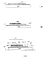
【解決手段】 流体用導管は、基板440に取り付けられた固定部453と、基板440から離れる曲がりを有するカンチレバー部454とを有するばねビーム460を含む。このばねビーム460は、該ばねビーム460のカンチレバー部454に沿って流体を運ぶための、カンチレバー部454の曲がりに対して略平行に延びる第1のチャネル452を定める。
【選択図】 図12
Description
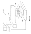
330A 分配システム
350A チャネルばねプローブ
300B つけペン式ナノリソグラフィ(DPN)システム
330B マイクロペンアセンブリ
350B チャネルばねプローブ
380B コンピュータ/ワークステーション
300C 流体回路
320C(1) 流体素子
320C(2) 流体素子
350C(1) チャネルばねプローブ
350C(2) チャネルばねプローブ
Claims (6)
- 基板に取り付けられた固定部と、前記基板から離れる曲がりを有するカンチレバー部とを有するばねビームを含む、流体用導管であって、前記ばねビームが、該ばねビームの前記カンチレバー部に沿って流体を運ぶための、前記カンチレバー部の前記曲がりに対して略平行に延びる第1のチャネルを定める、流体用導管。
- 剥離材料層の上に、該剥離材料層に対して垂直な方向の内部応力勾配を有するばね材料膜を形成する工程と、
ばね材料アイランドを形成するために、前記ばね材料膜をエッチングする工程と、
前記ばね材料アイランドのカンチレバー部に、前記内部応力勾配に起因する前記剥離層の第2の部分から離れる曲がりを帯びさせるために、前記剥離材料層の第1の部分を前記ばね材料アイランドの前記カンチレバー部の下から除去する工程と、
前記ばねビームの前記カンチレバー部に沿って流体を運ぶための、前記カンチレバー部の前記曲がりに対して略平行に延びる第1のチャネルを定める工程と、
を含む、流体用導管を形成する方法。 - 複数の流体サンプルを同時に分析するマイクロアレイシステムであって、
第1のパターンに配列された複数の試験位置を含む分析用集積回路(IC)と、
基板に取り付けられた固定端部と、自由端部の曲がりに対して平行に延びる第1のチャネルと、前記基板から離れる曲がりを有すると共に前記第1のチャネルから液体を分配するための分配先端部で終端する前記自由端部と、を各々が有する複数のチャネルばねプローブを含む分配アセンブリであって、前記複数のチャネルばねプローブの前記分配先端部が、前記第1のパターンと略一致する第2のパターンに配列された、分配アセンブリと、
前記複数のチャネルばねプローブの各々の前記分配先端部を、前記分析用IC上の前記複数の試験位置の1つと接触するよう配置するための配置システムと、
前記配置システムを制御すると共に前記分析用ICによって供給されるデータを処理するためのコンピュータ/ワークステーションと、
を含むマイクロアレイシステム。 - 基板をパターニングするためのつけペン式ナノリソグラフィ(DPN)システムであって、
基板を支持及び配置するための台と、
基板に取り付けられた固定端部と、自由端部の曲がりに対して平行に延びるチャネルと、前記基板から離れる曲がりを有すると共に前記チャネルから前記基板の上に液体を分配するための分配先端部で終端する前記自由端部と、を有する第1のチャネルばねプローブを含むマイクロペンアセンブリと、
前記第1のチャネルばねプローブの前記分配先端部を、前記基板と接触するよう配置すると共に、前記基板の上に所望のパターンをプリントするための配置システムと、
前記配置システムを制御するためのコンピュータ/ワークステーションと、
を有するDPNシステム。 - 第1の面を有する第1の流体素子と、
前記第1の面に取り付けられた固定部と、前記第1の面から離れる曲がりを有する自由部と、前記チャネルばねプローブの自由部に沿って流体を運ぶためのチャネルとを有するチャネルばねプローブと、
を有する流体回路。 - 複数のプリント用先端部を有するマイクロアレイの製造方法であって、
剥離材料層の上に、該剥離材料層に対して垂直な方向の内部応力勾配を有するばね材料膜を形成する工程と、
複数のばね材料アイランドをアレイパターンに形成するために、前記ばね材料膜をエッチングする工程と、
前記剥離材料層の第2の部分から離れる曲がりを各々が有する複数のばねビームであって、前記複数のプリント用先端部の1つを各々が構成する複数のばねビームを形成するために、前記剥離材料層の第1の部分を各前記ばね材料アイランドの前記カンチレバー部の下から除去する工程と、
を含む、マイクロアレイの製造方法。
Applications Claiming Priority (1)
| Application Number | Priority Date | Filing Date | Title |
|---|---|---|---|
| US10/213,059 US7241420B2 (en) | 2002-08-05 | 2002-08-05 | Capillary-channel probes for liquid pickup, transportation and dispense using stressy metal |
Publications (1)
| Publication Number | Publication Date |
|---|---|
| JP2004106172A true JP2004106172A (ja) | 2004-04-08 |
Family
ID=30443701
Family Applications (1)
| Application Number | Title | Priority Date | Filing Date |
|---|---|---|---|
| JP2003286395A Pending JP2004106172A (ja) | 2002-08-05 | 2003-08-05 | 流体用導管、流体用導管を形成する方法、マイクロアレイシステム、dpnシステム、流体回路、及びマイクロアレイの製造方法 |
Country Status (3)
| Country | Link |
|---|---|
| US (4) | US7241420B2 (ja) |
| EP (2) | EP1388369B1 (ja) |
| JP (1) | JP2004106172A (ja) |
Cited By (9)
| Publication number | Priority date | Publication date | Assignee | Title |
|---|---|---|---|---|
| JP2006055991A (ja) * | 2004-08-20 | 2006-03-02 | Palo Alto Research Center Inc | 応力固有素材及び形状記憶素材を使用したmemsデバイス並びにその製造方法 |
| JP2007535681A (ja) * | 2004-04-30 | 2007-12-06 | バイオフォース・ナノサイエンシィズ・インコーポレーテッド | 物質を表面上に堆積させるための方法と装置 |
| KR100812189B1 (ko) | 2007-04-24 | 2008-03-12 | 한국생산기술연구원 | 나노유체를 이용해 제어되는 캔틸레버 |
| JP2009534200A (ja) * | 2006-04-19 | 2009-09-24 | ノースウエスタン ユニバーシティ | 2次元ペン配列を有する並列リソグラフィのための物品 |
| JP2010527441A (ja) * | 2007-05-09 | 2010-08-12 | ナノインク インコーポレーティッド | 小型ナノファブリケーション装置 |
| CN101844443A (zh) * | 2009-03-26 | 2010-09-29 | 精工爱普生株式会社 | 喷液头、喷液装置及致动装置 |
| WO2014188649A1 (ja) * | 2013-05-23 | 2014-11-27 | パナソニックIpマネジメント株式会社 | 発電装置 |
| JP2015056663A (ja) * | 2013-09-10 | 2015-03-23 | パロ・アルト・リサーチ・センター・インコーポレーテッドPalo Alto Research Center Incorporated | 太陽電池のテクスチャリング |
| JP7449876B2 (ja) | 2018-11-16 | 2024-03-14 | イルミナ インコーポレイテッド | 流体カートリッジ用積層流体回路 |
Families Citing this family (43)
| Publication number | Priority date | Publication date | Assignee | Title |
|---|---|---|---|---|
| US20030054543A1 (en) * | 1997-06-16 | 2003-03-20 | Lafferty William Michael | Device for moving a selected station of a holding plate to a predetermined location for interaction with a probe |
| US20030148539A1 (en) * | 2001-11-05 | 2003-08-07 | California Institute Of Technology | Micro fabricated fountain pen apparatus and method for ultra high density biological arrays |
| GB0128350D0 (en) | 2001-11-27 | 2002-01-16 | Lab901 Ltd | Non-rigid apparatus for microfluidic applications |
| US7241420B2 (en) * | 2002-08-05 | 2007-07-10 | Palo Alto Research Center Incorporated | Capillary-channel probes for liquid pickup, transportation and dispense using stressy metal |
| US8080221B2 (en) * | 2002-08-05 | 2011-12-20 | Palo Alto Research Center Incorporated | Capillary-channel probes for liquid pickup, transportation and dispense using stressy metal |
| US8071168B2 (en) | 2002-08-26 | 2011-12-06 | Nanoink, Inc. | Micrometric direct-write methods for patterning conductive material and applications to flat panel display repair |
| US7034854B2 (en) * | 2002-11-12 | 2006-04-25 | Nanoink, Inc. | Methods and apparatus for ink delivery to nanolithographic probe systems |
| US20040233250A1 (en) * | 2003-03-05 | 2004-11-25 | Haushalter Robert C. | Microcontact printhead device |
| US7250139B2 (en) * | 2003-03-19 | 2007-07-31 | Northwestern University | Nanotipped device and method |
| US7217396B2 (en) | 2003-05-05 | 2007-05-15 | The Board Of Trustees Of The University Of Illinois | Microfabricated micro fluid channels |
| US20040228962A1 (en) | 2003-05-16 | 2004-11-18 | Chang Liu | Scanning probe microscopy probe and method for scanning probe contact printing |
| IL157206A0 (en) * | 2003-08-03 | 2004-02-19 | Correlating spatial position of chemical species on a substrate with molecular weight, structure and chemical reactivity | |
| US20050079711A1 (en) * | 2003-10-10 | 2005-04-14 | Cabot Microelectronics Corp. | Hollow tip array with nanometer size openings and formation thereof |
| CA2543091C (en) * | 2003-10-24 | 2013-09-03 | John Austin | Apparatus and method for dispensing fluid, semi-solid and solid samples |
| CA2557472C (en) * | 2004-02-25 | 2013-05-07 | Nanoink, Inc. | Micrometric direct-write methods for patterning conductive material and applications to flat panel display repair |
| US7819822B2 (en) * | 2004-03-06 | 2010-10-26 | Roche Diagnostics Operations, Inc. | Body fluid sampling device |
| ES2541680T3 (es) * | 2004-03-06 | 2015-07-23 | F. Hoffmann-La Roche Ag | Dispositivo de muestreo de líquidos corporales |
| US7775087B2 (en) * | 2004-03-16 | 2010-08-17 | Northwestern University | Microchannel forming method and nanotipped dispensing device having a microchannel |
| US20050236566A1 (en) * | 2004-04-26 | 2005-10-27 | Chang Liu | Scanning probe microscope probe with integrated capillary channel |
| WO2006012509A2 (en) * | 2004-07-23 | 2006-02-02 | Afa Controls, Llc | Methods of operating microvalve assemblies and related structures and related devices |
| DE102004050466A1 (de) * | 2004-10-16 | 2006-04-20 | Olympus Diagnostica Lab Automation Gmbh | Vorrichtung zum Pipettieren |
| EP1658897A1 (en) * | 2004-11-22 | 2006-05-24 | Roche Diagnostics GmbH | Bent microfluidic device |
| GB0502556D0 (en) * | 2005-02-08 | 2005-03-16 | Lab901 Ltd | Analysis instrument |
| US20080279727A1 (en) * | 2005-03-01 | 2008-11-13 | Haushalter Robert C | Polymeric Fluid Transfer and Printing Devices |
| CN100578228C (zh) | 2005-09-09 | 2010-01-06 | 博奥生物有限公司 | 一种微量液体精密分配仪器及其使用方法 |
| US7281419B2 (en) | 2005-09-21 | 2007-10-16 | The Board Of Trustees Of The University Of Illinois | Multifunctional probe array system |
| US20090093735A1 (en) * | 2006-03-29 | 2009-04-09 | Stephan Korner | Test unit and test system for analyzing body fluids |
| US8192794B2 (en) | 2006-04-19 | 2012-06-05 | Northwestern University | Massively parallel lithography with two-dimensional pen arrays |
| CN100405539C (zh) * | 2006-07-27 | 2008-07-23 | 华中科技大学 | 一种直写电子/光电子元器件的微细笔及由其构成的装置 |
| US8252160B2 (en) * | 2006-07-28 | 2012-08-28 | Hewlett-Packard Development Company, L.P. | Prevention of fluid delivered to reservoir from wicking into channels within microfluidic device |
| GB2445739A (en) | 2007-01-16 | 2008-07-23 | Lab901 Ltd | Polymeric laminates containing heat seals |
| AU2009210719A1 (en) * | 2008-02-05 | 2009-08-13 | Nanoink, Inc. | Array and cantilever array leveling |
| US8130072B2 (en) * | 2009-05-14 | 2012-03-06 | Palo Alto Research Center Incorporated | Vanadium oxide thermal microprobes |
| US8393785B2 (en) * | 2009-05-14 | 2013-03-12 | Palo Alto Research Center Incorporated | Nanocalorimeter based on thermal probes |
| US8579414B2 (en) | 2009-12-23 | 2013-11-12 | Xerox Corporation | Self-assembling structures for electrostatic extraction of pigments from liquid inks for marking |
| CN102270257B (zh) * | 2011-06-30 | 2013-02-06 | 南京开瑞汽车技术有限公司 | 一种流体通道的设计、计算方法 |
| US20150044686A1 (en) * | 2012-03-16 | 2015-02-12 | Life Technologies Corporation | Systems and Methods for Containing Biological Samples |
| CN102718182B (zh) * | 2012-07-10 | 2015-05-20 | 西南交通大学 | 一种多点接触模式下的大面积摩擦诱导微米级加工设备 |
| US10082500B2 (en) | 2013-08-22 | 2018-09-25 | Franz Baudenbacher | Device and method for detecting a target analyte |
| US9815261B2 (en) * | 2013-09-25 | 2017-11-14 | GM Global Technology Operations LLC | Applications of a reversible dry adhesive system |
| WO2017123652A1 (en) | 2016-01-11 | 2017-07-20 | Verndari, Inc. | Microneedle compositions and methods of using same |
| EP3493872A4 (en) * | 2016-08-03 | 2020-04-08 | Verndari, Inc. | MICROARRAYS AND METHOD |
| CN111747375B (zh) * | 2020-07-08 | 2023-08-11 | 河南大学 | 一种用于调控p-Si/n-ZnO薄膜异质结电学性能和光电输出的方法 |
Family Cites Families (21)
| Publication number | Priority date | Publication date | Assignee | Title |
|---|---|---|---|---|
| US3842189A (en) | 1973-01-08 | 1974-10-15 | Rca Corp | Contact array and method of making the same |
| US5063081A (en) * | 1988-11-14 | 1991-11-05 | I-Stat Corporation | Method of manufacturing a plurality of uniform microfabricated sensing devices having an immobilized ligand receptor |
| CA2071960C (en) | 1990-02-20 | 1994-08-23 | Hugh Ansley Thompson | Open capillary channel structures, improved process for making capillary channel structures, and extrusion die for use therein |
| JPH07103996A (ja) | 1993-10-06 | 1995-04-21 | Oki Electric Ind Co Ltd | ガスフローセンサ及びその形成方法 |
| DE4437260C1 (de) * | 1994-10-18 | 1995-10-19 | Siemens Ag | Mikromechanisches Relais |
| US5613861A (en) | 1995-06-07 | 1997-03-25 | Xerox Corporation | Photolithographically patterned spring contact |
| KR0185329B1 (ko) * | 1996-03-27 | 1999-05-15 | 이형도 | 기록액의 운동 관성을 이용한 기록 장치 |
| JP2001505640A (ja) | 1996-12-11 | 2001-04-24 | ゲーシム・ゲゼルシャフト・フューア・ズィリーツィウム−ミクロズュステーメ・ミト・ベシュレンクテル・ハフツング | マイクロポンプ |
| US6396966B1 (en) | 1997-02-09 | 2002-05-28 | Nanoptics, Inc. | Glass structures for nanodelivery and nanosensing |
| US6101946A (en) | 1997-11-21 | 2000-08-15 | Telechem International Inc. | Microarray printing device including printing pins with flat tips and exterior channel and method of manufacture |
| US6159368A (en) * | 1998-10-29 | 2000-12-12 | The Perkin-Elmer Corporation | Multi-well microfiltration apparatus |
| US6827979B2 (en) | 1999-01-07 | 2004-12-07 | Northwestern University | Methods utilizing scanning probe microscope tips and products therefor or produced thereby |
| US6888362B2 (en) * | 2000-11-09 | 2005-05-03 | Formfactor, Inc. | Test head assembly for electronic components with plurality of contoured microelectronic spring contacts |
| AU2573801A (en) | 1999-11-02 | 2001-05-14 | University Of Hawaii | Method for fabricating arrays of micro-needles |
| US6213789B1 (en) * | 1999-12-15 | 2001-04-10 | Xerox Corporation | Method and apparatus for interconnecting devices using an adhesive |
| JP3650722B2 (ja) | 2000-05-18 | 2005-05-25 | 株式会社アドバンテスト | プローブカードおよびその製造方法 |
| US6766817B2 (en) | 2001-07-25 | 2004-07-27 | Tubarc Technologies, Llc | Fluid conduction utilizing a reversible unsaturated siphon with tubarc porosity action |
| AU2003211027A1 (en) * | 2002-03-27 | 2003-10-13 | Nanoink, Inc. | Method and apparatus for aligning patterns on a substrate |
| US6668628B2 (en) * | 2002-03-29 | 2003-12-30 | Xerox Corporation | Scanning probe system with spring probe |
| FR2839662B1 (fr) | 2002-05-16 | 2005-12-02 | Centre Nat Rech Scient | Dispositif de depot localise d'au moins une solution biologique |
| US7241420B2 (en) * | 2002-08-05 | 2007-07-10 | Palo Alto Research Center Incorporated | Capillary-channel probes for liquid pickup, transportation and dispense using stressy metal |
-
2002
- 2002-08-05 US US10/213,059 patent/US7241420B2/en not_active Expired - Fee Related
-
2003
- 2003-07-28 EP EP20030254696 patent/EP1388369B1/en not_active Expired - Fee Related
- 2003-07-28 EP EP10181968.8A patent/EP2311567B1/en not_active Expired - Lifetime
- 2003-08-05 JP JP2003286395A patent/JP2004106172A/ja active Pending
-
2005
- 2005-11-03 US US11/267,762 patent/US7749448B2/en active Active
-
2009
- 2009-04-22 US US12/428,397 patent/US8241509B2/en active Active
-
2010
- 2010-05-06 US US12/775,452 patent/US8287744B2/en not_active Expired - Fee Related
Cited By (9)
| Publication number | Priority date | Publication date | Assignee | Title |
|---|---|---|---|---|
| JP2007535681A (ja) * | 2004-04-30 | 2007-12-06 | バイオフォース・ナノサイエンシィズ・インコーポレーテッド | 物質を表面上に堆積させるための方法と装置 |
| JP2006055991A (ja) * | 2004-08-20 | 2006-03-02 | Palo Alto Research Center Inc | 応力固有素材及び形状記憶素材を使用したmemsデバイス並びにその製造方法 |
| JP2009534200A (ja) * | 2006-04-19 | 2009-09-24 | ノースウエスタン ユニバーシティ | 2次元ペン配列を有する並列リソグラフィのための物品 |
| KR100812189B1 (ko) | 2007-04-24 | 2008-03-12 | 한국생산기술연구원 | 나노유체를 이용해 제어되는 캔틸레버 |
| JP2010527441A (ja) * | 2007-05-09 | 2010-08-12 | ナノインク インコーポレーティッド | 小型ナノファブリケーション装置 |
| CN101844443A (zh) * | 2009-03-26 | 2010-09-29 | 精工爱普生株式会社 | 喷液头、喷液装置及致动装置 |
| WO2014188649A1 (ja) * | 2013-05-23 | 2014-11-27 | パナソニックIpマネジメント株式会社 | 発電装置 |
| JP2015056663A (ja) * | 2013-09-10 | 2015-03-23 | パロ・アルト・リサーチ・センター・インコーポレーテッドPalo Alto Research Center Incorporated | 太陽電池のテクスチャリング |
| JP7449876B2 (ja) | 2018-11-16 | 2024-03-14 | イルミナ インコーポレイテッド | 流体カートリッジ用積層流体回路 |
Also Published As
| Publication number | Publication date |
|---|---|
| US7241420B2 (en) | 2007-07-10 |
| EP1388369A2 (en) | 2004-02-11 |
| EP2311567A1 (en) | 2011-04-20 |
| US20090233815A1 (en) | 2009-09-17 |
| EP2311567B1 (en) | 2013-05-08 |
| US20040022681A1 (en) | 2004-02-05 |
| US7749448B2 (en) | 2010-07-06 |
| EP1388369A3 (en) | 2004-12-29 |
| US8287744B2 (en) | 2012-10-16 |
| US20060057031A1 (en) | 2006-03-16 |
| US20100213161A1 (en) | 2010-08-26 |
| EP1388369B1 (en) | 2015-04-29 |
| US8241509B2 (en) | 2012-08-14 |
Similar Documents
| Publication | Publication Date | Title |
|---|---|---|
| JP2004106172A (ja) | 流体用導管、流体用導管を形成する方法、マイクロアレイシステム、dpnシステム、流体回路、及びマイクロアレイの製造方法 | |
| US6642129B2 (en) | Parallel, individually addressable probes for nanolithography | |
| US7523650B2 (en) | Multifunctional probe array system | |
| US6668628B2 (en) | Scanning probe system with spring probe | |
| EP1698905B9 (en) | Nano-drive for high resolution positioning and for positioning of a multi-point probe | |
| US8080221B2 (en) | Capillary-channel probes for liquid pickup, transportation and dispense using stressy metal | |
| US8261662B1 (en) | Active pen nanolithography | |
| US20110163061A1 (en) | Method Of Producing Microsprings Having Nanowire Tip Structures | |
| US20080230856A1 (en) | Intermediate probe structures for atomic force microscopy | |
| EP2535725A1 (en) | A probe for scanning probe microscopy | |
| EP1544865B1 (en) | A method for making probes for atomic force microscopy | |
| US10384230B2 (en) | Method for producing a substrate structured by nanowires, produced substrate, and use of the substrate |
Legal Events
| Date | Code | Title | Description |
|---|---|---|---|
| A621 | Written request for application examination |
Free format text: JAPANESE INTERMEDIATE CODE: A621 Effective date: 20060727 |
|
| A977 | Report on retrieval |
Free format text: JAPANESE INTERMEDIATE CODE: A971007 Effective date: 20081211 |
|
| A131 | Notification of reasons for refusal |
Free format text: JAPANESE INTERMEDIATE CODE: A131 Effective date: 20090120 |
|
| A601 | Written request for extension of time |
Free format text: JAPANESE INTERMEDIATE CODE: A601 Effective date: 20090417 |
|
| A521 | Request for written amendment filed |
Free format text: JAPANESE INTERMEDIATE CODE: A523 Effective date: 20090422 |
|
| A602 | Written permission of extension of time |
Free format text: JAPANESE INTERMEDIATE CODE: A602 Effective date: 20090422 |
|
| A02 | Decision of refusal |
Free format text: JAPANESE INTERMEDIATE CODE: A02 Effective date: 20090901 |