EP1544865B1 - Verfahren zur Herstellung von Sonden für Atomkraftmikroskopie - Google Patents
Verfahren zur Herstellung von Sonden für Atomkraftmikroskopie Download PDFInfo
- Publication number
- EP1544865B1 EP1544865B1 EP04447272A EP04447272A EP1544865B1 EP 1544865 B1 EP1544865 B1 EP 1544865B1 EP 04447272 A EP04447272 A EP 04447272A EP 04447272 A EP04447272 A EP 04447272A EP 1544865 B1 EP1544865 B1 EP 1544865B1
- Authority
- EP
- European Patent Office
- Prior art keywords
- holder
- probe
- contact region
- substrate
- pads
- Prior art date
- Legal status (The legal status is an assumption and is not a legal conclusion. Google has not performed a legal analysis and makes no representation as to the accuracy of the status listed.)
- Expired - Lifetime
Links
- 239000000523 sample Substances 0.000 title claims description 116
- 238000000034 method Methods 0.000 title claims description 29
- 238000004630 atomic force microscopy Methods 0.000 title claims description 9
- 239000000758 substrate Substances 0.000 claims description 60
- 239000000126 substance Substances 0.000 claims description 14
- 239000004065 semiconductor Substances 0.000 claims description 12
- 238000005530 etching Methods 0.000 claims description 9
- 238000004519 manufacturing process Methods 0.000 claims description 5
- 239000000463 material Substances 0.000 description 11
- 238000007747 plating Methods 0.000 description 11
- 238000000059 patterning Methods 0.000 description 9
- KWYUFKZDYYNOTN-UHFFFAOYSA-M potassium hydroxide Inorganic materials [OH-].[K+] KWYUFKZDYYNOTN-UHFFFAOYSA-M 0.000 description 9
- XUIMIQQOPSSXEZ-UHFFFAOYSA-N Silicon Chemical compound [Si] XUIMIQQOPSSXEZ-UHFFFAOYSA-N 0.000 description 8
- 229910052710 silicon Inorganic materials 0.000 description 8
- 239000010703 silicon Substances 0.000 description 8
- HEMHJVSKTPXQMS-UHFFFAOYSA-M Sodium hydroxide Chemical compound [OH-].[Na+] HEMHJVSKTPXQMS-UHFFFAOYSA-M 0.000 description 3
- 229910003460 diamond Inorganic materials 0.000 description 3
- 239000010432 diamond Substances 0.000 description 3
- 238000001459 lithography Methods 0.000 description 3
- ZOXJGFHDIHLPTG-UHFFFAOYSA-N Boron Chemical compound [B] ZOXJGFHDIHLPTG-UHFFFAOYSA-N 0.000 description 2
- 239000004593 Epoxy Substances 0.000 description 2
- WMFOQBRAJBCJND-UHFFFAOYSA-M Lithium hydroxide Chemical compound [Li+].[OH-] WMFOQBRAJBCJND-UHFFFAOYSA-M 0.000 description 2
- 229910052581 Si3N4 Inorganic materials 0.000 description 2
- VYPSYNLAJGMNEJ-UHFFFAOYSA-N Silicium dioxide Chemical compound O=[Si]=O VYPSYNLAJGMNEJ-UHFFFAOYSA-N 0.000 description 2
- 229910052796 boron Inorganic materials 0.000 description 2
- HUCVOHYBFXVBRW-UHFFFAOYSA-M caesium hydroxide Chemical compound [OH-].[Cs+] HUCVOHYBFXVBRW-UHFFFAOYSA-M 0.000 description 2
- 230000000694 effects Effects 0.000 description 2
- 230000005496 eutectics Effects 0.000 description 2
- 239000011521 glass Substances 0.000 description 2
- 239000002184 metal Substances 0.000 description 2
- 229910052751 metal Inorganic materials 0.000 description 2
- 239000007769 metal material Substances 0.000 description 2
- 238000005459 micromachining Methods 0.000 description 2
- 229920000642 polymer Polymers 0.000 description 2
- CPRMKOQKXYSDML-UHFFFAOYSA-M rubidium hydroxide Chemical compound [OH-].[Rb+] CPRMKOQKXYSDML-UHFFFAOYSA-M 0.000 description 2
- HQVNEWCFYHHQES-UHFFFAOYSA-N silicon nitride Chemical compound N12[Si]34N5[Si]62N3[Si]51N64 HQVNEWCFYHHQES-UHFFFAOYSA-N 0.000 description 2
- 229910052814 silicon oxide Inorganic materials 0.000 description 2
- 229910000679 solder Inorganic materials 0.000 description 2
- 238000005476 soldering Methods 0.000 description 2
- WGTYBPLFGIVFAS-UHFFFAOYSA-M tetramethylammonium hydroxide Chemical compound [OH-].C[N+](C)(C)C WGTYBPLFGIVFAS-UHFFFAOYSA-M 0.000 description 2
- VHUUQVKOLVNVRT-UHFFFAOYSA-N Ammonium hydroxide Chemical compound [NH4+].[OH-] VHUUQVKOLVNVRT-UHFFFAOYSA-N 0.000 description 1
- OKTJSMMVPCPJKN-UHFFFAOYSA-N Carbon Chemical compound [C] OKTJSMMVPCPJKN-UHFFFAOYSA-N 0.000 description 1
- PIICEJLVQHRZGT-UHFFFAOYSA-N Ethylenediamine Chemical compound NCCN PIICEJLVQHRZGT-UHFFFAOYSA-N 0.000 description 1
- GRYLNZFGIOXLOG-UHFFFAOYSA-N Nitric acid Chemical compound O[N+]([O-])=O GRYLNZFGIOXLOG-UHFFFAOYSA-N 0.000 description 1
- 239000004642 Polyimide Substances 0.000 description 1
- 229910007637 SnAg Inorganic materials 0.000 description 1
- 229910008433 SnCU Inorganic materials 0.000 description 1
- 229910007116 SnPb Inorganic materials 0.000 description 1
- 239000000853 adhesive Substances 0.000 description 1
- 238000004026 adhesive bonding Methods 0.000 description 1
- 230000001070 adhesive effect Effects 0.000 description 1
- 229910052782 aluminium Inorganic materials 0.000 description 1
- 238000004458 analytical method Methods 0.000 description 1
- 230000015572 biosynthetic process Effects 0.000 description 1
- 229910052799 carbon Inorganic materials 0.000 description 1
- 239000000919 ceramic Substances 0.000 description 1
- 230000001419 dependent effect Effects 0.000 description 1
- 230000008021 deposition Effects 0.000 description 1
- 239000002019 doping agent Substances 0.000 description 1
- 229910052732 germanium Inorganic materials 0.000 description 1
- GNPVGFCGXDBREM-UHFFFAOYSA-N germanium atom Chemical compound [Ge] GNPVGFCGXDBREM-UHFFFAOYSA-N 0.000 description 1
- 239000012535 impurity Substances 0.000 description 1
- 239000007788 liquid Substances 0.000 description 1
- 229910044991 metal oxide Inorganic materials 0.000 description 1
- 150000004706 metal oxides Chemical class 0.000 description 1
- 229910017604 nitric acid Inorganic materials 0.000 description 1
- 239000004033 plastic Substances 0.000 description 1
- 229920001721 polyimide Polymers 0.000 description 1
- 229910021426 porous silicon Inorganic materials 0.000 description 1
- 230000002035 prolonged effect Effects 0.000 description 1
- 229910052709 silver Inorganic materials 0.000 description 1
- 239000007787 solid Substances 0.000 description 1
- 238000009987 spinning Methods 0.000 description 1
- 238000005211 surface analysis Methods 0.000 description 1
- 229910052718 tin Inorganic materials 0.000 description 1
- 229910052719 titanium Inorganic materials 0.000 description 1
- 238000012876 topography Methods 0.000 description 1
Images


Classifications
-
- G—PHYSICS
- G01—MEASURING; TESTING
- G01Q—SCANNING-PROBE TECHNIQUES OR APPARATUS; APPLICATIONS OF SCANNING-PROBE TECHNIQUES, e.g. SCANNING PROBE MICROSCOPY [SPM]
- G01Q60/00—Particular types of SPM [Scanning Probe Microscopy] or microscopes; Essential components thereof
- G01Q60/24—AFM [Atomic Force Microscopy] or apparatus therefor, e.g. AFM probes
- G01Q60/38—Probes, their manufacture, or their related instrumentation, e.g. holders
Definitions
- the present invention is related to probes for Atomic Force Microscopy (AFM).
- AFM Atomic Force Microscopy
- Such a probe consists of a probe tip, a cantilever and a probe holder chip.
- the invention is related to a method for manufacturing a probe of this type.
- Atomic Force Microscopy is a well established surface analysis technique for analysing the topography and electrical characteristics of semiconductor samples.
- the technique involves the use of a moving probe in contact with the surface under analysis.
- An AFM probe generally consists of a cantilever, a tip at one end of the cantilever and a holder at the other end.
- the holder is a large body of material used to handle the probe and is preferably located at the opposite side of the probe tip, i.e. at the side pointing in the opposite direction of the tip, this to prevent the holder from touching the sample's surface.
- a first type of probe having a silicon tip, manufactured by Si bulk micromachining, is known in the art.
- the kind of probe to which the invention is related has a tip that is moulded into a silicon substrate. This is illustrated for example in document US-A-5399232. Of this type, probes with silicon nitride tip and cantilever are the most common. In all cases of this kind, the tip is pointing inwards towards the substrate.
- the holder can be attached by anodic bonding, or by adhesive, eutectic or solder bonding. It can be formed above the wafer by plating or out of thick resist. Often, a full glass wafer is bonded and then diced on the substrate to form individual holders.
- the probe tip and cantilever are underetched prior to peel-off, but the rest of the probe structure, particularly the part on which the holder is to be attached is too large to be fully underetched. This has also made it impossible so far to release the probe from the front side after bonding or forming of a holder. No sacrificial layer has been found to be really practical for release under a 1.5X3mm holder piece. Either the etch rate is too slow or the release chemical is overly harmful to the probe. Underetching the Si wafer under the probe is not an option either, since Si is etched slowly in KOH or another anisotropic etchant.
- top side release of a probe before holder attachment in this case a diamond probe is to be found in 'CVD diamond probes for nanotechnology', Niedermann et al., Appl. Phys. A66, S31-S34 (1998).
- the film comprising the cantilever forms a pattern that is mostly in the ⁇ 100> direction although the probe including the cantilever is still oriented in the general ⁇ 110> direction.
- An example of front side release of patterned microstructures by underetching the Si substrate in isotropic etchant can be found in WO-A-9418697.
- Document US-A-6215137 is related to a probe with a thermocouple made of a joint between a first metal material and a second metal material. To release the probes, etching from the backside of the substrate is performed.
- Document EP-A-1189016 is related to a soldering procedure, for mounting a probe to a holder chip, after the substrate carrying the probe has been etched from the backside of the substrate.
- the present invention aims to provide a method for producing probes with a moulded tip, which does not suffer from the disadvantages of the prior art.
- the present invention is related to a method and a product having the characteristics described in the appended independent claims 1 and 10. Preferred embodiments are subject of the dependent claims.
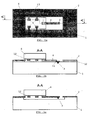
- Fig. 1a represents in top view a preferred embodiment of a probe configuration used in the method of the invention.
- Figures 1b and 1c represent sectioned views of two alternatives, respectively with or without a sacrificial layer.
- Fig. 2 represents another probe configuration according to the invention.
- Fig. 3 and 4 represent probe configurations with three probe tips.
- Fig. 5 represents the way in which a holder substrate may be diced after attachment.
- Fig. 6a to 6c represents ways of increasing the gap between the holder and the substrate.
- Fig. 7 represents an alternative, involving a plated holder.
- Fig. 8 represents another alternative, involving a holder comprising holes through the thickness.
- the probe configuration is made in such a way that the contact region consists of one or more separate, elevated bonding pads, the total surface of these pads being smaller than the surface area of the holder region which is to be attached to these pads.
- the holder is then attached to these pads, by a known technique, for example bonding or soldering.
- the probe and holder are separated from the substrate by underetching with a release chemical from the front side of the substrate.
- the contact region can be fully underetched due to the reduced size of this contact region.
- the height of the pads must be sufficient to allow the release chemical to flow underneath the attached holder, into a gap formed between the holder and the substrate.
- the difference in size between the contact region and the holder needs to be sufficient in order to allow the creation of said gap over a large area of the substrate surface which is covered by the holder.
- the pads are only surrounded by a gutter, and the gap is formed by the thickness of a bonding layer attached to the pads (see fig. 2).
- a sacrificial layer may be applied before creating the probe configuration. Such a sacrificial layer will facilitate the release.
- Figure 1a illustrates a preferred embodiment of the invention. It shows a top view of the substrate 1 wherein the probe configuration is equally visible.
- This configuration comprises the probe tip 3 (possibly made of a different material than the probe layer), the cantilever 4 and the contact region, comprising four bonding pads 5.
- the large rectangle indicates the place where the holder 6 will be placed.
- the part 7 of the cantilever which is to be covered by the holder, can be viewed as a fifth bonding pad.
- the bonding pads 5 and 7 thereby define the contact region.
- the probe configuration is produced by applying a probe layer 2, and subsequently patterning this layer.
- Figure 1b shows a first embodiment wherein a sacrificial layer 10 is applied before applying the probe layer 2. It is to be noted that the sacrificial layer is patterned prior to the application of the probe layer, so that a small area 11 around the tip is not covered by said sacrificial layer.
- the probe layer 2 is applied on top of the sacrificial layer and subsequently patterned to obtain the bonding pads 5,7 and the cantilever 4, lying on top of the sacrificial layer 10.
- the patterning of the probe layer takes place in a known way, by applying resist and performing a lithography step. What is obtained after this step is the probe configuration, being still attached to the substrate and consisting of the pads 5 and 7, the cantilever 4 and the tip 3.
- a bonding layer 12 may be applied to the bonding pads by plating, etching back or lift-off.
- the bonding layer can itself be a photosensitive layer, patterned directly by lithography.
- the holder 6 is attached to said bonding layer 12.
- the bonding layer can also be applied to the holder, or to the pads and the holder.
- the bonding layer may be absent, and the holder may be attached directly to the bonding pads.
- the under-etch takes place with the help of a release chemical, which may be a liquid or gas phase, i.e. vapour HF or a plasma, and which can flow in the gap between the substrate and the holder.
- the sacrificial layer 10 is etched away.
- the substrate is etched.
- the underetching of the pads, cantilever and tip can take place quickly due to the reduced area of the pads, allowing the release of the whole structure in a short time, thereby avoiding the risk of damaging the probe by a prolonged contact with the release chemical.
- the pads 5 remain attached to the probe layer 2 through strips 13, which can be broken prior to the final removal of the probe structure.
- Figure 1c shows an embodiment without the use of a sacrificial layer, and wherein the substrate 1 is underetched.
- Figure 2 shows an embodiment, wherein the patterning of the probe layer is done in such a way that only a zone 20 around the pads 5 and the cantilever 4 is removed.
- the bonding layer 12 provides the necessary distance between the holder 6 and the probe layer 2, allowing the release chemical to flow in the 'gutters' 20 around the bonding pads 5.
- the thickness of the bonding layer is therefore an important parameter in this embodiment.
- Small contact Si-areas 14 remain between the substrate and the probe configuration. The dimensions of the bonding pads and the etch times should be such that these contact areas are obtained.
- the pads are preferably much longer than wide and oriented in a ⁇ 100> direction. After the under-etch, these areas 14 can be broken or the probe can be peeled off for a full removal. A similar process is possible using a sacrificial layer.
- Figures 3 and 4 show other embodiments.
- a probe configuration comprising three probe tips is attached to one holder 6.
- Three bonding pads 7 are connected to the respective cantilevers 4, while three separate bonding pads 5 are present, connected to the substrate by breakable strips 13.
- Figure 4 shows a probe structure wherein the bonding pads 7 which are in connection with a probe cantilever and tip stretch over the full length of the contact region. Besides these, there are three small pads 5, connected to the probe layer by strips 13. The release chemical must flow into the long channels between the pads 7 in order to underetch the pads from the side.
- the holders are not individually bonded to the probes.
- a full wafer is preferably bonded on top of a substrate whereon a plurality of probe configurations has been created. As shown in figure 5, this wafer is then diced to form individual holders before release.
- Figure 6a shows an embodiment wherein a pre-etching of the sacrificial layer 10 is performed, prior to the holder attachment.
- Figure 6b shows an embodiment wherein a pre-etch of the holder is performed, while figure 6c shows an embodiment involving a pre-etch of the substrate. All embodiments of figures 6a to 6c are aimed at increasing the gap between the substrate surface and the holder, in order to facilitate the flow of release chemical into this gap.
- the present invention is equally related to other ways of producing AFM probes by releasing from the front side, after holder attachment.
- One embodiment in this respect is shown in figure 7, and involves the creation of holders by plating.
- the probe layer comprising the tip 3 and cantilever 4 is prepared as in the previous embodiments.
- the probe layer is patterned for a number of probes simultaneously so that it contains a number of long parallel pads separated by gaps, similar to the pattern shown in figure 4.
- the holder is not attached onto the pads, but a thick resist layer is applied on top of the probe configuration, and patterned so that areas 21 of resist remain in the gaps.
- the holder is then created by plating, for example a layer of Ni 22, on top of the probe configurations.
- the plating process is continued until the resist-filled gaps are almost sealed off, as shown in figure 7a. At this point, the resist is removed, leaving the gaps empty to create channels 25, and the plating is continued until a holder layer 23 is obtained.
- the channels allow the underetching of the probe configuration to take place in the above described way, by release chemical flowing into the channels and underetching the pads from the side.
- Another embodiment of the invention makes use of a holder or holder substrate comprising holes 24 through the thickness (see fig.8), bonded or formed in another way including plating, or thick resist patterning to a probe layer which is not necessarily patterned to comprise bonding pads, but which is patterned to have openings aligned with the holes in the holder. These openings equally have the effect of reducing the surface of the contact region so that this contact region is smaller than the surface area of the holder region which is to be attached to said contact region.
- the holes allow the flow of release chemical to said contact region between the holder and the probe configuration and consequently between the probe configuration and the sacrificial layer or the Si substrate, so that the contact region can be underetched and a release from the front side becomes possible.
- the total contact region between the probe and the substrate after bonding is less than 0.5mm 2 .
- the substrate is preferably monocrystalline, preferably ⁇ 100>, silicon.
- the probe configuration may be created by applying a probe layer, for example a silicon nitride layer or a metal layer, and subsequently patterning this layer by known lithography techniques.
- the probe layer may also consist of silicon oxide, a plastic including SU-8 or a hardmetal.
- the probe configuration may be obtained by a plating technique, by plating onto a previously patterned seed layer, or wherein a patterning step is performed on a resist layer, before plating the probe configuration selectively in the regions where there is no resist, and thereafter removing the resist.
- a plating technique by plating onto a previously patterned seed layer, or wherein a patterning step is performed on a resist layer, before plating the probe configuration selectively in the regions where there is no resist, and thereafter removing the resist.
- damascene process wherein the probe layer is plated onto a previously patterned resist layer, and subsequently polished, whereafter the resist is removed.
- the probe layer can also be formed by implanting or diffusing impurities such as a dopant (such as boron) or another element such as carbon. Such a layer is etched more slowly (about 10 times for highly boron doped Si) in KOH than undoped Si. The Cantilever will then be patterned into the Si wafer (bulk micromachining). Such a probe layer would be underetched the same way as a deposited layer.
- impurities such as a dopant (such as boron) or another element such as carbon.
- the holder may be silicon or glass in the case of a separately attached holder or holder substrate.
- Ni may be used, as described above in relation to figure 7. If a photosensitive polymer (resist) is used, photosensitive epoxy (SU-8) is the most reasonable.
- the holder may be active, meaning that it may incorporate active devices such as transistors.
- the holder may be attached by solder bonding including SnPb, Sn, Ag, SnAg, SnCu, SnBi. It may be done using adhesive bonding including Epoxy (SU-8), Polyimide, BCB, anodic bonding or eutectic bonding. A holder may equally be created by spinning and patterning a thick resist layer.
- the shape of the bonding pads is such that no point on these pads is further than 300 ⁇ m away from the edge of the pad.
- a sacrificial layer can be used : silicon, porous silicon, Germanium, silicon oxide, Al, Ti, polymer, or others.
- the underetching of the silicon substrate itself may be performed using an anisotropic etchant, such as KOH, TMAH, NaOH, NH 4 OH, RbOH, CsOH, LiOH, ethylenediamine (EDP).
- the probe is preferably rotated with respect to the wafer north-south direction, and aligned with a ⁇ 100> direction of the Si-substrate.
- the patterns may be aligned with the ⁇ 100> direction while the probe is oriented in another direction.
- Direct isotropic etching of the silicon substrate may be done by using an etchant based on nitric acid or HCl or other.
Landscapes
- Physics & Mathematics (AREA)
- Health & Medical Sciences (AREA)
- General Health & Medical Sciences (AREA)
- General Physics & Mathematics (AREA)
- Nuclear Medicine, Radiotherapy & Molecular Imaging (AREA)
- Radiology & Medical Imaging (AREA)
- Measuring Leads Or Probes (AREA)
- Testing Or Measuring Of Semiconductors Or The Like (AREA)
Claims (10)
- Verfahren zum Herstellen von Sonden für die Atomkraftmikroskopie, umfassend die Schritte:- Bereitstellen eines Halbleitersubstrates (1),- Herstellen auf der Oberfläche einer Seite des Halbleitsubstrates einer oder mehrerer Matrizen zur Herstellung einer oder mehrerer Sondenspitzen,- Herstellen auf der einen Seite des Halbleitersubstrates einer oder mehrerer Sondenanordnungen, wobei jede Anordnung einen Kontaktbereich zum Anbringen einer Haltevorrichtung und in Verbindung mit dem Kontaktbereich mindestens einen Satz aus einer Sondenspitze (3) und einem Ausleger (4) umfasst,- Anbringen einer oder mehrerer Haltevorrichtungen (6) an jedem der Kontaktbereiche,dadurch gekennzeichnet, dass- der Flächeninhalt jedes Kontaktbereiches kleiner ist als der Flächeninhalt des Haltevorrichtungsbereiches, der an dem Kontaktbereich angebracht werden soll, und- das Verfahren ferner den Schritt des Ablösens der Struktur, welche die Sondenanordnung und die Haltevorrichtung umfasst, von dem Halbleitersubstrat durch Unterätzen der Sondenanordnung von der Seite des Halbleitersubstrates her, auf der die Sondenanordnung hergestellt wird, umfasst, wobei der Schritt des Unterätzens nach dem Schritt des Anbringens einer Haltevorrichtung erfolgt.
- Verfahren nach Anspruch 1, wobei der Kontaktbereich ein oder mehrere Bindeplättchen (5, 7) umfasst und der Gesamtflächeninhalt der Plättchen kleiner ist als der Flächeninhalt des Haltevorrichtungsbereiches, der an den Plättchen angebracht werden soll.
- Verfahren nach Anspruch 2, wobei die Bindeplättchen so groß sind, dass kein Punkt auf der Oberfläche eines Plättchens weiter als 300 µm von dem Rand des Plättchens entfernt ist.
- Verfahren nach Anspruch 2, wobei die Plättchen gestreckt sind und zwischen benachbarten Plättchen Kanäle gebildet werden.
- Verfahren nach Anspruch 1, wobei die Haltevorrichtung mehrere Löcher (24) umfasst, um zu ermöglichen, dass eine Ablösechemikalie den Kontaktbereich erreicht, und wobei der Kontaktbereich so hergestellt wird, dass er eine Anzahl von Öffnungen umfasst, die an den Löchern ausgerichtet sind, die das Unterätzen der Sondenanordnung ermöglichen.
- Verfahren nach Anspruch 1 bis 5, wobei der Schritt des Anbringens einer Haltevorrichtung (6) durch Verbinden erfolgt und das Verfahren ferner den Schritt des Auftragens einer Bindeschicht (12) auf den Kontaktbereich oder die Haltevorrichtung oder auf beide umfasst, bevor die Haltevorrichtung angebracht wird.
- Verfahren nach einem der Ansprüche 1 bis 6, wobei die Höhe des Kontaktbereiches oder die Höhe des Kontaktbereiches und der Bindeschicht (12) zusammen ausreicht, um zwischen der Haltevorrichtung und dem Substrat einen Spalt zu erzeugen, um so zu ermöglichen, dass eine Ablösechemikalie zwischen die Haltevorrichtung und das Substrat fließt.
- Verfahren nach einem der vorhergehenden Ansprüche, ferner umfassend den Schritt des Auftragens einer Opferschicht (10) auf das Substrat (1), bevor die Sondenanordnung (2) erzeugt wird.
- Verfahren nach einem der vorhergehenden Ansprüche, wobei die Haltevorrichtung durch das Anbringen eines Haltevorrichtungssubstrates auf ein Substrat, das mehrere Sondenanordnungen umfasst, angebracht wird und wobei das Haltevorrichtungssubstrat zur Bildung einzelner Haltevorrichtungen zu Scheibchen geschnitten wird, wobei der Schritt des Schneidens zu Scheibchen vor dem Schritt des Ablösens der Haltevorrichtungen erfolgt.
- Halbfertig-Sondenstruktur für die Atomkraftmikroskopie, umfassend:ein Halbleitersubstrat (1) mit einer oder mehreren Matrizen, die auf der Oberfläche einer Seite des Halbleitersubstrates gebildet sind, zur Herstellung einer oder mehrerer Sondenspitzen;eine oder mehrere Sondenanordnungen, die auf der Seite des Halbleitersubstrates gebildet sind, wobei jede Sondenanordnung einen Kontaktbereich und mindestens einen Satz aus einer Sondenspitze (3) und einem Ausleger (4) umfasst und wobei jeder Kontaktbereich ein oder mehrere Bindeplättchen umfasst; undeine oder mehrere Haltevorrichtungen (6), die an jedem der Kontaktbereiche angebracht sind,dadurch gekennzeichnet, dass ein Flächeninhalt der mehreren Bindeplättchen zusammen kleiner ist als ein Flächeninhalt der Haltevorrichtung, die an dem Kontaktbereich angebracht ist, und wobei eine Höhe der Bindeplättchen ausreicht, um zu ermöglichen, dass eine Ablösechemikalie von der einen Seite des Halbleitersubstrates in einen Spalt zwischen der Haltevorrichtung und dem Halbleitersubstrat fließt.
Priority Applications (1)
| Application Number | Priority Date | Filing Date | Title |
|---|---|---|---|
| EP04447272A EP1544865B1 (de) | 2003-12-17 | 2004-12-10 | Verfahren zur Herstellung von Sonden für Atomkraftmikroskopie |
Applications Claiming Priority (3)
| Application Number | Priority Date | Filing Date | Title |
|---|---|---|---|
| EP03447294A EP1548748A1 (de) | 2003-12-17 | 2003-12-17 | Verfahren zur Herstellung von Sonden für Atomkraftmikroskopie |
| EP03447294 | 2003-12-17 | ||
| EP04447272A EP1544865B1 (de) | 2003-12-17 | 2004-12-10 | Verfahren zur Herstellung von Sonden für Atomkraftmikroskopie |
Publications (2)
| Publication Number | Publication Date |
|---|---|
| EP1544865A1 EP1544865A1 (de) | 2005-06-22 |
| EP1544865B1 true EP1544865B1 (de) | 2007-02-14 |
Family
ID=34524789
Family Applications (1)
| Application Number | Title | Priority Date | Filing Date |
|---|---|---|---|
| EP04447272A Expired - Lifetime EP1544865B1 (de) | 2003-12-17 | 2004-12-10 | Verfahren zur Herstellung von Sonden für Atomkraftmikroskopie |
Country Status (1)
| Country | Link |
|---|---|
| EP (1) | EP1544865B1 (de) |
Families Citing this family (2)
| Publication number | Priority date | Publication date | Assignee | Title |
|---|---|---|---|---|
| FR3107962B1 (fr) * | 2020-03-09 | 2022-03-04 | Vmicro | Dispositif de détection pour microscope à sonde locale |
| CN112158794B (zh) * | 2020-09-04 | 2024-03-22 | 杭州探真纳米科技有限公司 | 一种采用等离子体刻蚀制备原子力显微镜探针阶梯型基底的方法 |
Family Cites Families (4)
| Publication number | Priority date | Publication date | Assignee | Title |
|---|---|---|---|---|
| CA2154357C (en) * | 1993-02-04 | 2004-03-02 | Kevin A. Shaw | Microstructures and single-mask, single-crystal process for fabrication thereof |
| JPH1194863A (ja) * | 1997-09-12 | 1999-04-09 | Nikon Corp | カンチレバー及びその製造方法 |
| EP1189016B1 (de) * | 2000-09-15 | 2009-04-22 | Interuniversitair Micro-Elektronica Centrum Vzw | Verfahren zur Herstellung montierter AFM-Sonden durch Löten |
| EP1202047A1 (de) * | 2000-10-27 | 2002-05-02 | Interuniversitair Micro-Elektronica Centrum | Herstellungsverfahren für Spitzen und Probenköpfen von STM's oder AFM's |
-
2004
- 2004-12-10 EP EP04447272A patent/EP1544865B1/de not_active Expired - Lifetime
Also Published As
| Publication number | Publication date |
|---|---|
| EP1544865A1 (de) | 2005-06-22 |
Similar Documents
| Publication | Publication Date | Title |
|---|---|---|
| US8089294B2 (en) | MEMS probe fabrication on a reusable substrate for probe card application | |
| Albrecht et al. | Microfabrication of cantilever styli for the atomic force microscope | |
| US7281419B2 (en) | Multifunctional probe array system | |
| JP2004106172A (ja) | 流体用導管、流体用導管を形成する方法、マイクロアレイシステム、dpnシステム、流体回路、及びマイクロアレイの製造方法 | |
| JP4733319B2 (ja) | プローブチップ構造の製造方法 | |
| US8828243B2 (en) | Scanning probe having integrated silicon tip with cantilever | |
| CN1935632B (zh) | 制造纳米线器件的方法 | |
| EP1431241A2 (de) | Fühlerfingerstruktur und Herstellungsverfahren für eine Fühlerfingerstruktur | |
| JP2003307483A (ja) | ばねプローブを有する走査プローブシステム | |
| US20080121029A1 (en) | Cantilever with carbon nano-tube for AFM | |
| US20080230856A1 (en) | Intermediate probe structures for atomic force microscopy | |
| EP1544865B1 (de) | Verfahren zur Herstellung von Sonden für Atomkraftmikroskopie | |
| Rangelow et al. | Fabrication of piezoresistive-sensed AFM cantilever probe with integrated tip | |
| CN110482484B (zh) | 一种低成本的基于应力剥离技术的微悬臂梁的制备方法 | |
| JP2010517055A (ja) | 原子間力顕微鏡法用のビデオレートを可能とするプローブ | |
| AU781887B2 (en) | Production of diaphragms | |
| US7598107B1 (en) | Semi-sacrificial mold for diamond structures | |
| JP7554208B2 (ja) | ピラミッド状突起を含むmemsデバイスを提供する方法、及び型 | |
| Fujita et al. | Nanoelectromechanical Systems | |
| EP1491950B1 (de) | Mikrobauteil und Verfahren zu seiner Herstellung | |
| JPH09304411A (ja) | カンチレバー及びカンチレバー連結体並びにそれらの製造方法 | |
| JPH05299015A (ja) | 走査型プローブ顕微鏡用カンチレバーの作製方法 | |
| JPH11311627A (ja) | マイクロセンサデバイスの製造方法 | |
| Cho et al. | Si-based micro probe card with sharp knife-edged tips combined metal deposition | |
| EP0588888A1 (de) | Mikroprobe für einen oberflächen-rastermikroskop. |
Legal Events
| Date | Code | Title | Description |
|---|---|---|---|
| PUAI | Public reference made under article 153(3) epc to a published international application that has entered the european phase |
Free format text: ORIGINAL CODE: 0009012 |
|
| AK | Designated contracting states |
Kind code of ref document: A1 Designated state(s): AT BE BG CH CY CZ DE DK EE ES FI FR GB GR HU IE IS IT LI LT LU MC NL PL PT RO SE SI SK TR |
|
| AX | Request for extension of the european patent |
Extension state: AL BA HR LV MK YU |
|
| 17P | Request for examination filed |
Effective date: 20050809 |
|
| AKX | Designation fees paid |
Designated state(s): AT BE BG CH CY CZ DE DK EE ES FI FR GB GR HU IE IS IT LI LT LU MC NL PL PT RO SE SI SK TR |
|
| GRAP | Despatch of communication of intention to grant a patent |
Free format text: ORIGINAL CODE: EPIDOSNIGR1 |
|
| GRAS | Grant fee paid |
Free format text: ORIGINAL CODE: EPIDOSNIGR3 |
|
| GRAA | (expected) grant |
Free format text: ORIGINAL CODE: 0009210 |
|
| AK | Designated contracting states |
Kind code of ref document: B1 Designated state(s): AT BE BG CH CY CZ DE DK EE ES FI FR GB GR HU IE IS IT LI LT LU MC NL PL PT RO SE SI SK TR |
|
| PG25 | Lapsed in a contracting state [announced via postgrant information from national office to epo] |
Ref country code: PL Free format text: LAPSE BECAUSE OF FAILURE TO SUBMIT A TRANSLATION OF THE DESCRIPTION OR TO PAY THE FEE WITHIN THE PRESCRIBED TIME-LIMIT Effective date: 20070214 Ref country code: CH Free format text: LAPSE BECAUSE OF FAILURE TO SUBMIT A TRANSLATION OF THE DESCRIPTION OR TO PAY THE FEE WITHIN THE PRESCRIBED TIME-LIMIT Effective date: 20070214 Ref country code: LI Free format text: LAPSE BECAUSE OF FAILURE TO SUBMIT A TRANSLATION OF THE DESCRIPTION OR TO PAY THE FEE WITHIN THE PRESCRIBED TIME-LIMIT Effective date: 20070214 Ref country code: DK Free format text: LAPSE BECAUSE OF FAILURE TO SUBMIT A TRANSLATION OF THE DESCRIPTION OR TO PAY THE FEE WITHIN THE PRESCRIBED TIME-LIMIT Effective date: 20070214 Ref country code: NL Free format text: LAPSE BECAUSE OF FAILURE TO SUBMIT A TRANSLATION OF THE DESCRIPTION OR TO PAY THE FEE WITHIN THE PRESCRIBED TIME-LIMIT Effective date: 20070214 Ref country code: AT Free format text: LAPSE BECAUSE OF FAILURE TO SUBMIT A TRANSLATION OF THE DESCRIPTION OR TO PAY THE FEE WITHIN THE PRESCRIBED TIME-LIMIT Effective date: 20070214 Ref country code: BE Free format text: LAPSE BECAUSE OF FAILURE TO SUBMIT A TRANSLATION OF THE DESCRIPTION OR TO PAY THE FEE WITHIN THE PRESCRIBED TIME-LIMIT Effective date: 20070214 Ref country code: SI Free format text: LAPSE BECAUSE OF FAILURE TO SUBMIT A TRANSLATION OF THE DESCRIPTION OR TO PAY THE FEE WITHIN THE PRESCRIBED TIME-LIMIT Effective date: 20070214 Ref country code: FI Free format text: LAPSE BECAUSE OF FAILURE TO SUBMIT A TRANSLATION OF THE DESCRIPTION OR TO PAY THE FEE WITHIN THE PRESCRIBED TIME-LIMIT Effective date: 20070214 |
|
| REG | Reference to a national code |
Ref country code: GB Ref legal event code: FG4D |
|
| REG | Reference to a national code |
Ref country code: CH Ref legal event code: EP |
|
| REF | Corresponds to: |
Ref document number: 602004004732 Country of ref document: DE Date of ref document: 20070329 Kind code of ref document: P |
|
| REG | Reference to a national code |
Ref country code: IE Ref legal event code: FG4D |
|
| PG25 | Lapsed in a contracting state [announced via postgrant information from national office to epo] |
Ref country code: SE Free format text: LAPSE BECAUSE OF FAILURE TO SUBMIT A TRANSLATION OF THE DESCRIPTION OR TO PAY THE FEE WITHIN THE PRESCRIBED TIME-LIMIT Effective date: 20070514 Ref country code: BG Free format text: LAPSE BECAUSE OF FAILURE TO SUBMIT A TRANSLATION OF THE DESCRIPTION OR TO PAY THE FEE WITHIN THE PRESCRIBED TIME-LIMIT Effective date: 20070514 |
|
| PG25 | Lapsed in a contracting state [announced via postgrant information from national office to epo] |
Ref country code: ES Free format text: LAPSE BECAUSE OF FAILURE TO SUBMIT A TRANSLATION OF THE DESCRIPTION OR TO PAY THE FEE WITHIN THE PRESCRIBED TIME-LIMIT Effective date: 20070525 |
|
| PG25 | Lapsed in a contracting state [announced via postgrant information from national office to epo] |
Ref country code: IS Free format text: LAPSE BECAUSE OF FAILURE TO SUBMIT A TRANSLATION OF THE DESCRIPTION OR TO PAY THE FEE WITHIN THE PRESCRIBED TIME-LIMIT Effective date: 20070614 |
|
| PG25 | Lapsed in a contracting state [announced via postgrant information from national office to epo] |
Ref country code: PT Free format text: LAPSE BECAUSE OF FAILURE TO SUBMIT A TRANSLATION OF THE DESCRIPTION OR TO PAY THE FEE WITHIN THE PRESCRIBED TIME-LIMIT Effective date: 20070716 |
|
| NLV1 | Nl: lapsed or annulled due to failure to fulfill the requirements of art. 29p and 29m of the patents act | ||
| ET | Fr: translation filed | ||
| REG | Reference to a national code |
Ref country code: CH Ref legal event code: PL |
|
| PG25 | Lapsed in a contracting state [announced via postgrant information from national office to epo] |
Ref country code: SK Free format text: LAPSE BECAUSE OF FAILURE TO SUBMIT A TRANSLATION OF THE DESCRIPTION OR TO PAY THE FEE WITHIN THE PRESCRIBED TIME-LIMIT Effective date: 20070214 |
|
| PLBE | No opposition filed within time limit |
Free format text: ORIGINAL CODE: 0009261 |
|
| STAA | Information on the status of an ep patent application or granted ep patent |
Free format text: STATUS: NO OPPOSITION FILED WITHIN TIME LIMIT |
|
| PG25 | Lapsed in a contracting state [announced via postgrant information from national office to epo] |
Ref country code: RO Free format text: LAPSE BECAUSE OF FAILURE TO SUBMIT A TRANSLATION OF THE DESCRIPTION OR TO PAY THE FEE WITHIN THE PRESCRIBED TIME-LIMIT Effective date: 20070214 Ref country code: CZ Free format text: LAPSE BECAUSE OF FAILURE TO SUBMIT A TRANSLATION OF THE DESCRIPTION OR TO PAY THE FEE WITHIN THE PRESCRIBED TIME-LIMIT Effective date: 20070214 |
|
| 26N | No opposition filed |
Effective date: 20071115 |
|
| PG25 | Lapsed in a contracting state [announced via postgrant information from national office to epo] |
Ref country code: LT Free format text: LAPSE BECAUSE OF FAILURE TO SUBMIT A TRANSLATION OF THE DESCRIPTION OR TO PAY THE FEE WITHIN THE PRESCRIBED TIME-LIMIT Effective date: 20070214 |
|
| PG25 | Lapsed in a contracting state [announced via postgrant information from national office to epo] |
Ref country code: IT Free format text: LAPSE BECAUSE OF FAILURE TO SUBMIT A TRANSLATION OF THE DESCRIPTION OR TO PAY THE FEE WITHIN THE PRESCRIBED TIME-LIMIT Effective date: 20070214 Ref country code: GR Free format text: LAPSE BECAUSE OF FAILURE TO SUBMIT A TRANSLATION OF THE DESCRIPTION OR TO PAY THE FEE WITHIN THE PRESCRIBED TIME-LIMIT Effective date: 20070515 |
|
| PG25 | Lapsed in a contracting state [announced via postgrant information from national office to epo] |
Ref country code: MC Free format text: LAPSE BECAUSE OF NON-PAYMENT OF DUE FEES Effective date: 20071231 |
|
| PG25 | Lapsed in a contracting state [announced via postgrant information from national office to epo] |
Ref country code: IE Free format text: LAPSE BECAUSE OF NON-PAYMENT OF DUE FEES Effective date: 20071210 |
|
| PG25 | Lapsed in a contracting state [announced via postgrant information from national office to epo] |
Ref country code: EE Free format text: LAPSE BECAUSE OF FAILURE TO SUBMIT A TRANSLATION OF THE DESCRIPTION OR TO PAY THE FEE WITHIN THE PRESCRIBED TIME-LIMIT Effective date: 20070214 |
|
| PG25 | Lapsed in a contracting state [announced via postgrant information from national office to epo] |
Ref country code: CY Free format text: LAPSE BECAUSE OF FAILURE TO SUBMIT A TRANSLATION OF THE DESCRIPTION OR TO PAY THE FEE WITHIN THE PRESCRIBED TIME-LIMIT Effective date: 20070214 |
|
| PG25 | Lapsed in a contracting state [announced via postgrant information from national office to epo] |
Ref country code: LU Free format text: LAPSE BECAUSE OF NON-PAYMENT OF DUE FEES Effective date: 20071210 |
|
| PG25 | Lapsed in a contracting state [announced via postgrant information from national office to epo] |
Ref country code: TR Free format text: LAPSE BECAUSE OF FAILURE TO SUBMIT A TRANSLATION OF THE DESCRIPTION OR TO PAY THE FEE WITHIN THE PRESCRIBED TIME-LIMIT Effective date: 20070214 Ref country code: HU Free format text: LAPSE BECAUSE OF FAILURE TO SUBMIT A TRANSLATION OF THE DESCRIPTION OR TO PAY THE FEE WITHIN THE PRESCRIBED TIME-LIMIT Effective date: 20070815 |
|
| REG | Reference to a national code |
Ref country code: FR Ref legal event code: PLFP Year of fee payment: 12 |
|
| REG | Reference to a national code |
Ref country code: FR Ref legal event code: PLFP Year of fee payment: 13 |
|
| REG | Reference to a national code |
Ref country code: FR Ref legal event code: PLFP Year of fee payment: 14 |
|
| PGFP | Annual fee paid to national office [announced via postgrant information from national office to epo] |
Ref country code: FR Payment date: 20201120 Year of fee payment: 17 Ref country code: DE Payment date: 20201119 Year of fee payment: 17 Ref country code: GB Payment date: 20201123 Year of fee payment: 17 |
|
| REG | Reference to a national code |
Ref country code: DE Ref legal event code: R119 Ref document number: 602004004732 Country of ref document: DE |
|
| GBPC | Gb: european patent ceased through non-payment of renewal fee |
Effective date: 20211210 |
|
| PG25 | Lapsed in a contracting state [announced via postgrant information from national office to epo] |
Ref country code: GB Free format text: LAPSE BECAUSE OF NON-PAYMENT OF DUE FEES Effective date: 20211210 Ref country code: DE Free format text: LAPSE BECAUSE OF NON-PAYMENT OF DUE FEES Effective date: 20220701 |
|
| PG25 | Lapsed in a contracting state [announced via postgrant information from national office to epo] |
Ref country code: FR Free format text: LAPSE BECAUSE OF NON-PAYMENT OF DUE FEES Effective date: 20211231 |