EP1548748A1 - Verfahren zur Herstellung von Sonden für Atomkraftmikroskopie - Google Patents
Verfahren zur Herstellung von Sonden für Atomkraftmikroskopie Download PDFInfo
- Publication number
- EP1548748A1 EP1548748A1 EP03447294A EP03447294A EP1548748A1 EP 1548748 A1 EP1548748 A1 EP 1548748A1 EP 03447294 A EP03447294 A EP 03447294A EP 03447294 A EP03447294 A EP 03447294A EP 1548748 A1 EP1548748 A1 EP 1548748A1
- Authority
- EP
- European Patent Office
- Prior art keywords
- holder
- probe
- substrate
- contact region
- pads
- Prior art date
- Legal status (The legal status is an assumption and is not a legal conclusion. Google has not performed a legal analysis and makes no representation as to the accuracy of the status listed.)
- Withdrawn
Links
- 238000000034 method Methods 0.000 title claims 11
- 239000000523 sample Substances 0.000 title claims 10
- 238000004630 atomic force microscopy Methods 0.000 title claims 2
- 239000000758 substrate Substances 0.000 claims 10
- 238000005530 etching Methods 0.000 claims 2
- 238000004519 manufacturing process Methods 0.000 claims 2
- 239000000126 substance Substances 0.000 claims 2
- 239000004065 semiconductor Substances 0.000 claims 1
Images


Classifications
-
- G—PHYSICS
- G01—MEASURING; TESTING
- G01Q—SCANNING-PROBE TECHNIQUES OR APPARATUS; APPLICATIONS OF SCANNING-PROBE TECHNIQUES, e.g. SCANNING PROBE MICROSCOPY [SPM]
- G01Q60/00—Particular types of SPM [Scanning Probe Microscopy] or microscopes; Essential components thereof
- G01Q60/24—AFM [Atomic Force Microscopy] or apparatus therefor, e.g. AFM probes
- G01Q60/38—Probes, their manufacture, or their related instrumentation, e.g. holders
-
- B—PERFORMING OPERATIONS; TRANSPORTING
- B82—NANOTECHNOLOGY
- B82Y—SPECIFIC USES OR APPLICATIONS OF NANOSTRUCTURES; MEASUREMENT OR ANALYSIS OF NANOSTRUCTURES; MANUFACTURE OR TREATMENT OF NANOSTRUCTURES
- B82Y35/00—Methods or apparatus for measurement or analysis of nanostructures
-
- Y—GENERAL TAGGING OF NEW TECHNOLOGICAL DEVELOPMENTS; GENERAL TAGGING OF CROSS-SECTIONAL TECHNOLOGIES SPANNING OVER SEVERAL SECTIONS OF THE IPC; TECHNICAL SUBJECTS COVERED BY FORMER USPC CROSS-REFERENCE ART COLLECTIONS [XRACs] AND DIGESTS
- Y10—TECHNICAL SUBJECTS COVERED BY FORMER USPC
- Y10T—TECHNICAL SUBJECTS COVERED BY FORMER US CLASSIFICATION
- Y10T29/00—Metal working
- Y10T29/42—Piezoelectric device making
-
- Y—GENERAL TAGGING OF NEW TECHNOLOGICAL DEVELOPMENTS; GENERAL TAGGING OF CROSS-SECTIONAL TECHNOLOGIES SPANNING OVER SEVERAL SECTIONS OF THE IPC; TECHNICAL SUBJECTS COVERED BY FORMER USPC CROSS-REFERENCE ART COLLECTIONS [XRACs] AND DIGESTS
- Y10—TECHNICAL SUBJECTS COVERED BY FORMER USPC
- Y10T—TECHNICAL SUBJECTS COVERED BY FORMER US CLASSIFICATION
- Y10T29/00—Metal working
- Y10T29/49—Method of mechanical manufacture
- Y10T29/49002—Electrical device making
- Y10T29/49117—Conductor or circuit manufacturing
- Y10T29/49124—On flat or curved insulated base, e.g., printed circuit, etc.
- Y10T29/49147—Assembling terminal to base
- Y10T29/49151—Assembling terminal to base by deforming or shaping
-
- Y—GENERAL TAGGING OF NEW TECHNOLOGICAL DEVELOPMENTS; GENERAL TAGGING OF CROSS-SECTIONAL TECHNOLOGIES SPANNING OVER SEVERAL SECTIONS OF THE IPC; TECHNICAL SUBJECTS COVERED BY FORMER USPC CROSS-REFERENCE ART COLLECTIONS [XRACs] AND DIGESTS
- Y10—TECHNICAL SUBJECTS COVERED BY FORMER USPC
- Y10T—TECHNICAL SUBJECTS COVERED BY FORMER US CLASSIFICATION
- Y10T29/00—Metal working
- Y10T29/49—Method of mechanical manufacture
- Y10T29/49002—Electrical device making
- Y10T29/49117—Conductor or circuit manufacturing
- Y10T29/49124—On flat or curved insulated base, e.g., printed circuit, etc.
- Y10T29/49155—Manufacturing circuit on or in base
-
- Y—GENERAL TAGGING OF NEW TECHNOLOGICAL DEVELOPMENTS; GENERAL TAGGING OF CROSS-SECTIONAL TECHNOLOGIES SPANNING OVER SEVERAL SECTIONS OF THE IPC; TECHNICAL SUBJECTS COVERED BY FORMER USPC CROSS-REFERENCE ART COLLECTIONS [XRACs] AND DIGESTS
- Y10—TECHNICAL SUBJECTS COVERED BY FORMER USPC
- Y10T—TECHNICAL SUBJECTS COVERED BY FORMER US CLASSIFICATION
- Y10T29/00—Metal working
- Y10T29/49—Method of mechanical manufacture
- Y10T29/49002—Electrical device making
- Y10T29/49117—Conductor or circuit manufacturing
- Y10T29/49204—Contact or terminal manufacturing
Definitions
- the present invention is related to probes for Atomic Force Microscopy (AFM).
- AFM Atomic Force Microscopy
- Such a probe consists of a probe tip, a cantilever and a probe holder chip.
- the invention is related to a method for manufacturing a probe of this type.
- Atomic Force Microscopy is a well established surface analysis technique for analysing the topography and electrical characteristics of semiconductor samples.
- the technique involves the use of a moving probe in contact with the surface under analysis.
- An AFM probe generally consists of a cantilever, a tip at one end of the cantilever and a holder at the other end.
- the holder is a large body of material used to handle the probe and is preferably located at the opposite side of the probe tip, i.e. at the side pointing in the opposite direction of the tip, this to prevent the holder from touching the sample's surface.
- the kind of probe to which the invention is related has a tip that is moulded into a silicon substrate. This is illustrated for example in document US-A-5399232. Of this type, probes with silicon nitride tip and cantilever are the most common. In all cases of this kind, the tip is pointing inwards towards the substrate.
- the holder can be attached by anodic bonding, or by adhesive, eutectic or solder bonding. It can be formed above the wafer by plating or out of thick resist. Often, a full glass wafer is bonded and then diced on the substrate to form individual holders.
- the probe tip and cantilever are underetched prior to peel-off, but the rest of the probe structure, particularly the part on which the holder is to be attached is too large to be fully underetched. This has also made it impossible so far to release the probe from the front side after bonding or forming of a holder. No sacrificial layer has been found to be really practical for release under a 1.5X3mm holder piece. Either the etch rate is too slow or the release chemical is overly harmful to the probe. Underetching the Si wafer under the probe is not an option either, since Si is etched slowly in KOH or another anisotropic etchant.
- top side release of a probe before holder attachment in this case a diamond probe is to be found in 'CVD diamond probes for nanotechnology', Niedermann et al., Appl. Phys. A66, S31-S34 (1998).
- the film comprising the cantilever forms a pattern that is mostly in the ⁇ 100> direction although the probe including the cantilever is still oriented in the general ⁇ 110> direction.
- An example of front side release of patterned microstructures by underetching the Si substrate in isotropic etchant can be found in WO-A-9418697. In this case the pattern does not need to be rotated in the ⁇ 100> direction.
- the present invention aims to provide a method for producing probes with a moulded tip, which does not suffer from the disadvantages of the prior art.
- the present invention is related to a method and a product having the characteristics described in the appended claims.
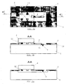
- Fig. 1a represents in top view a preferred embodiment of a probe configuration used in the method of the invention.
- Figures 1b and 1c represent sectioned views of two alternatives, respectively with or without a sacrificial layer.
- Fig. 2 represents another probe configuration according to the invention.
- Fig. 3 and 4 represent probe configurations with three probe tips.
- Fig. 5 represents the way in which a holder substrate may be diced after attachment.
- Fig. 6a to 6c represents ways of increasing the gap between the holder and the substrate.
- Fig. 7 represents an alternative, involving a plated holder.
- Fig. 8 represents another alternative, involving a holder comprising holes through the thickness.
- the method of the invention comprises firstly a number of steps which are known from the prior art :
- the probe configuration is made in such a way that the contact region consists of one or more separate, elevated bonding pads, the total surface of these pads being smaller than the surface area of the holder region which is to be attached to these pads.
- the holder is then attached to these pads, by a known technique, for example bonding or soldering.
- the probe and holder are separated from the substrate by underetching with a release chemical from the front side of the substrate.
- the contact region can be fully underetched due to the reduced size of this contact region.
- the height of the pads must be sufficient to allow the release chemical to flow underneath the attached holder, into a gap formed between the holder and the substrate.
- the difference in size between the contact region and the holder needs to be sufficient in order to allow the creation of said gap over a large area of the substrate surface which is covered by the holder.
- the pads are only surrounded by a gutter, and the gap is formed by the thickness of a bonding layer attached to the pads (see fig. 2).
- a sacrificial layer may be applied before creating the probe configuration. Such a sacrificial layer will facilitate the release.
- Figure 1a illustrates a preferred embodiment of the invention. It shows a top view of the substrate 1 wherein the probe configuration is equally visible.
- This configuration comprises the probe tip 3 (possibly made of a different material than the probe layer), the cantilever 4 and the contact region, comprising four bonding pads 5.
- the large rectangle indicates the place where the holder 6 will be placed.
- the part 7 of the cantilever which is to be covered by the holder, can be viewed as a fifth bonding pad.
- the bonding pads 5 and 7 thereby define the contact region.
- the probe configuration is produced by applying a probe layer 2, and subsequently patterning this layer.
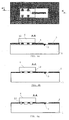
- Figure 1b shows a first embodiment wherein a sacrificial layer 10 is applied before applying the probe layer 2. It is to be noted that the sacrificial layer is patterned prior to the application of the probe layer, so that a small area 11 around the tip is not covered by said sacrificial layer.
- the probe layer 2 is applied on top of the sacrificial layer and subsequently patterned to obtain the bonding pads 5,7 and the cantilever 4, lying on top of the sacrificial layer 10.
- the patterning of the probe layer takes place in a known way, by applying resist and performing a lithography step. What is obtained after this step is the probe configuration, being still attached to the substrate and consisting of the pads 5 and 7, the cantilever 4 and the tip 3.
- a bonding layer 12 may be applied to the bonding pads by plating, etching back or lift-off.
- the bonding layer can itself be a photosensitive layer, patterned directly by lithography.
- the holder 6 is attached to said bonding layer 12.
- the bonding layer can also be applied to the holder, or to the pads and the holder.
- the bonding layer may be absent, and the holder may be attached directly to the bonding pads.
- the under-etch takes place with the help of a release chemical, which may be a liquid or gas phase, i.e. vapour HF or a plasma, and which can flow in the gap between the substrate and the holder.
- the sacrificial layer 10 is etched away.
- the substrate is etched.
- the underetching of the pads, cantilever and tip can take place quickly due to the reduced area of the pads, allowing the release of the whole structure in a short time, thereby avoiding the risk of damaging the probe by a prolonged contact with the release chemical.
- the pads 5 remain attached to the probe layer 2 through strips 13, which can be broken prior to the final removal of the probe structure.
- Figure 1c shows an embodiment without the use of a sacrificial layer, and wherein the substrate 1 is underetched.
- Figure 2 shows an embodiment, wherein the patterning of the probe layer is done in such a way that only a zone 20 around the pads 5 and the cantilever 4 is removed.
- the bonding layer 12 provides the necessary distance between the holder 6 and the probe layer 2, allowing the release chemical to flow in the 'gutters' 20 around the bonding pads 5.
- the thickness of the bonding layer is therefore an important parameter in this embodiment.
- Small contact Si-areas 14 remain between the substrate and the probe configuration. The dimensions of the bonding pads and the etch times should be such that these contact areas are obtained.
- the pads are preferably much longer than wide and oriented in a ⁇ 100> direction. After the under-etch, these areas 14 can be broken or the probe can be peeled off for a full removal. A similar process is possible using a sacrificial layer.
- Figures 3 and 4 show other embodiments.
- a probe configuration comprising three probe tips is attached to one holder 6.
- Three bonding pads 7 are connected to the respective cantilevers 4, while three separate bonding pads 5 are present, connected to the substrate by breakable strips 13.
- Figure 4 shows a probe structure wherein the bonding pads 7 which are in connection with a probe cantilever and tip stretch over the full length of the contact region. Besides these, there are three small pads 5, connected to the probe layer by strips 13. The release chemical must flow into the long channels between the pads 7 in order to underetch the pads from the side.
- the holders are not individually bonded to the probes.
- a full wafer is preferably bonded on top of a substrate whereon a plurality of probe configurations has been created. As shown in figure 5, this wafer is then diced to form individual holders before release.
- Figure 6a shows an embodiment wherein a pre-etching of the sacrificial layer 10 is performed, prior to the holder attachment.
- Figure 6b shows an embodiment wherein a pre-etch of the holder is performed, while figure 6c shows an embodiment involving a pre-etch of the substrate. All embodiments of figures 6a to 6c are aimed at increasing the gap between the substrate surface and the holder, in order to facilitate the flow of release chemical into this gap.
- the present invention is equally related to other ways of producing AFM probes by releasing from the front side, after holder attachment.
- One embodiment in this respect is shown in figure 7, and involves the creation of holders by plating.
- the probe layer comprising the tip 3 and cantilever 4 is prepared as in the previous embodiments.
- the probe layer is patterned for a number of probes simultaneously so that it contains a number of long parallel pads separated by gaps, similar to the pattern shown in figure 4.
- the holder is not attached onto the pads, but a thick resist layer is applied on top of the probe configuration, and patterned so that areas 21 of resist remain in the gaps.
- the holder is then created by plating, for example a layer of Ni 22, on top of the probe configurations.
- the plating process is continued until the resist-filled gaps are almost sealed off, as shown in figure 7a. At this point, the resist is removed, leaving the gaps empty to create channels 25, and the plating is continued until a holder layer 23 is obtained.
- the channels allow the underetching of the probe configuration to take place in the above described way, by release chemical flowing into the channels and underetching the pads from the side.
- Another embodiment of the invention makes use of a holder or holder substrate comprising holes 24 through the thickness (see fig.8), bonded or formed in another way including plating, or thick resist patterning to a probe layer which is not necessarily patterned to comprise bonding pads, but which is patterned to have openings aligned with the holes in the holder. These openings equally have the effect of reducing the surface of the contact region so that this contact region is smaller than the surface area of the holder region which is to be attached to said contact region.
- the holes allow the flow of release chemical to said contact region between the holder and the probe configuration and consequently between the probe configuration and the sacrificial layer or the Si substrate, so that the contact region can be underetched and a release from the front side becomes possible.
- the total contact region between the probe and the substrate after bonding is less than 0.5mm 2 .
- the substrate is preferably monocrystalline, preferably ⁇ 100>, silicon.
- the probe configuration may be created by applying a probe layer, for example a silicon nitride layer or a metal layer, and subsequently patterning this layer by known lithography techniques.
- the probe layer may also consist of silicon oxide, a plastic including SU-8 or a hardmetal.
- the probe configuration may be obtained by a plating technique, by plating onto a previously patterned seed layer, or wherein a patterning step is performed on a resist layer, before plating the probe configuration selectively in the regions where there is no resist, and thereafter removing the resist.
- a plating technique by plating onto a previously patterned seed layer, or wherein a patterning step is performed on a resist layer, before plating the probe configuration selectively in the regions where there is no resist, and thereafter removing the resist.
- damascene process wherein the probe layer is plated onto a previously patterned resist layer, and subsequently polished, whereafter the resist is removed.
- the probe layer can also be formed by implanting or diffusing impurities such as a dopant (such as boron) or another element such as carbon. Such a layer is etched more slowly (about 10 times for highly boron doped Si) in KOH than undoped Si. The Cantilever will then be patterned into the Si wafer (bulk micromachining). Such a probe layer would be underetched the same way as a deposited layer.
- impurities such as a dopant (such as boron) or another element such as carbon.
- the holder may be silicon or glass in the case of a separately attached holder or holder substrate.
- Ni may be used, as described above in relation to figure 7. If a photosensitive polymer (resist) is used, photosensitive epoxy (SU-8) is the most reasonable.
- the holder may be active, meaning that it may incorporate active devices such as transistors.
- the holder may be attached by solder bonding including SnPb, Sn, Ag, SnAg, SnCu, SnBi. It may be done using adhesive bonding including Epoxy (SU-8), Polyimide, BCB, anodic bonding or eutectic bonding. A holder may equally be created by spinning and patterning a thick resist layer.
- the shape of the bonding pads is such that no point on these pads is further than 300 ⁇ m away from the edge of the pad.
- a sacrificial layer can be used : silicon, porous silicon, Germanium, silicon oxide, Al, Ti, polymer, or others.
- the underetching of the silicon substrate itself may be performed using an anisotropic etchant, such as KOH, TMAH, NaOH, NH 4 OH, RbOH, CsOH, LiOH, ethylenediamine (EDP).
- the probe is preferably rotated with respect to the wafer north-south direction, and aligned with a ⁇ 100> direction of the Si-substrate.
- the patterns may be aligned with the ⁇ 100> direction while the probe is oriented in another direction.
- Direct isotropic etching of the silicon substrate may be done by using an etchant based on nitric acid or HCl or other.
Landscapes
- Chemical & Material Sciences (AREA)
- Nuclear Medicine, Radiotherapy & Molecular Imaging (AREA)
- Engineering & Computer Science (AREA)
- Nanotechnology (AREA)
- Physics & Mathematics (AREA)
- Health & Medical Sciences (AREA)
- General Health & Medical Sciences (AREA)
- General Physics & Mathematics (AREA)
- Radiology & Medical Imaging (AREA)
- Crystallography & Structural Chemistry (AREA)
- Analytical Chemistry (AREA)
- Measuring Leads Or Probes (AREA)
- Testing Or Measuring Of Semiconductors Or The Like (AREA)
- Investigating And Analyzing Materials By Characteristic Methods (AREA)
Priority Applications (7)
| Application Number | Priority Date | Filing Date | Title |
|---|---|---|---|
| EP03447294A EP1548748A1 (de) | 2003-12-17 | 2003-12-17 | Verfahren zur Herstellung von Sonden für Atomkraftmikroskopie |
| DE602004004732T DE602004004732T2 (de) | 2003-12-17 | 2004-12-10 | Verfahren zur Herstellung von Sonden für Atomkraftmikroskopie |
| AT04447272T ATE354168T1 (de) | 2003-12-17 | 2004-12-10 | Verfahren zur herstellung von sonden für atomkraftmikroskopie |
| EP04447272A EP1544865B1 (de) | 2003-12-17 | 2004-12-10 | Verfahren zur Herstellung von Sonden für Atomkraftmikroskopie |
| US11/015,715 US7240428B2 (en) | 2003-12-17 | 2004-12-16 | Method for making probes for atomic force microscopy |
| JP2004364670A JP4447447B2 (ja) | 2003-12-17 | 2004-12-16 | 原子間力顕微鏡検査用のプローブを製造する方法 |
| US11/775,183 US20080230856A1 (en) | 2003-12-17 | 2007-07-09 | Intermediate probe structures for atomic force microscopy |
Applications Claiming Priority (1)
| Application Number | Priority Date | Filing Date | Title |
|---|---|---|---|
| EP03447294A EP1548748A1 (de) | 2003-12-17 | 2003-12-17 | Verfahren zur Herstellung von Sonden für Atomkraftmikroskopie |
Publications (1)
| Publication Number | Publication Date |
|---|---|
| EP1548748A1 true EP1548748A1 (de) | 2005-06-29 |
Family
ID=34530882
Family Applications (1)
| Application Number | Title | Priority Date | Filing Date |
|---|---|---|---|
| EP03447294A Withdrawn EP1548748A1 (de) | 2003-12-17 | 2003-12-17 | Verfahren zur Herstellung von Sonden für Atomkraftmikroskopie |
Country Status (5)
| Country | Link |
|---|---|
| US (2) | US7240428B2 (de) |
| EP (1) | EP1548748A1 (de) |
| JP (1) | JP4447447B2 (de) |
| AT (1) | ATE354168T1 (de) |
| DE (1) | DE602004004732T2 (de) |
Families Citing this family (4)
| Publication number | Priority date | Publication date | Assignee | Title |
|---|---|---|---|---|
| JP5503096B2 (ja) | 2001-01-19 | 2014-05-28 | ヴィロノヴァティブ,ベスローテン ヴェンノートシャップ | 感受性哺乳動物において気道疾患を引き起こすウイルス |
| JP4553589B2 (ja) | 2002-02-21 | 2010-09-29 | メディミューン,エルエルシー | 組換えパラインフルエンザウイルス発現系とメタニューモウイルスから得られる異種抗原を含むワクチン |
| EP1748447B1 (de) * | 2005-07-28 | 2008-10-22 | Interuniversitair Microelektronica Centrum ( Imec) | Atomkraftmikroskop-Sonde mit einer doppelten Spitze und deren Herstellungsverfahren. |
| US8089294B2 (en) * | 2008-08-05 | 2012-01-03 | WinMENS Technologies Co., Ltd. | MEMS probe fabrication on a reusable substrate for probe card application |
Citations (4)
| Publication number | Priority date | Publication date | Assignee | Title |
|---|---|---|---|---|
| WO1994018697A1 (en) * | 1993-02-04 | 1994-08-18 | Cornell Research Foundation, Inc. | Microstructures and single mask, single-crystal process for fabrication thereof |
| US6215137B1 (en) * | 1997-09-12 | 2001-04-10 | Nikon Corporation | Micromechanical sensor for scanning thermal imaging microscope and method of making the same |
| EP1189016A1 (de) * | 2000-09-15 | 2002-03-20 | Interuniversitair Micro-Elektronica Centrum Vzw | Verfahren zur Herstellung von eingebauten AFM-Proben beim Löten |
| EP1202047A1 (de) * | 2000-10-27 | 2002-05-02 | Interuniversitair Micro-Elektronica Centrum | Herstellungsverfahren für Spitzen und Probenköpfen von STM's oder AFM's |
Family Cites Families (8)
| Publication number | Priority date | Publication date | Assignee | Title |
|---|---|---|---|---|
| US4423401A (en) * | 1982-07-21 | 1983-12-27 | Tektronix, Inc. | Thin-film electrothermal device |
| US4958585A (en) | 1988-07-11 | 1990-09-25 | Skeeter Products, Inc. | Boat hull |
| US5221415A (en) | 1989-01-17 | 1993-06-22 | Board Of Trustees Of The Leland Stanford Junior University | Method of forming microfabricated cantilever stylus with integrated pyramidal tip |
| JP3053456B2 (ja) * | 1990-08-31 | 2000-06-19 | オリンパス光学工業株式会社 | 走査型プローブ顕微鏡用カンチレバー及びその作製方法 |
| JP3109861B2 (ja) * | 1991-06-12 | 2000-11-20 | キヤノン株式会社 | 情報の記録及び/又は再生装置 |
| DE19642378C2 (de) * | 1996-10-14 | 2000-06-08 | Fraunhofer Ges Forschung | Kontaktlose Chipkarte |
| KR100746768B1 (ko) * | 2002-03-19 | 2007-08-06 | 주식회사 엘지이아이 | 캔틸레버를 이용한 정보 기록 및 판독 장치 |
| US7132723B2 (en) * | 2002-11-14 | 2006-11-07 | Raytheon Company | Micro electro-mechanical system device with piezoelectric thin film actuator |
-
2003
- 2003-12-17 EP EP03447294A patent/EP1548748A1/de not_active Withdrawn
-
2004
- 2004-12-10 AT AT04447272T patent/ATE354168T1/de not_active IP Right Cessation
- 2004-12-10 DE DE602004004732T patent/DE602004004732T2/de not_active Expired - Lifetime
- 2004-12-16 US US11/015,715 patent/US7240428B2/en not_active Expired - Lifetime
- 2004-12-16 JP JP2004364670A patent/JP4447447B2/ja not_active Expired - Fee Related
-
2007
- 2007-07-09 US US11/775,183 patent/US20080230856A1/en not_active Abandoned
Patent Citations (4)
| Publication number | Priority date | Publication date | Assignee | Title |
|---|---|---|---|---|
| WO1994018697A1 (en) * | 1993-02-04 | 1994-08-18 | Cornell Research Foundation, Inc. | Microstructures and single mask, single-crystal process for fabrication thereof |
| US6215137B1 (en) * | 1997-09-12 | 2001-04-10 | Nikon Corporation | Micromechanical sensor for scanning thermal imaging microscope and method of making the same |
| EP1189016A1 (de) * | 2000-09-15 | 2002-03-20 | Interuniversitair Micro-Elektronica Centrum Vzw | Verfahren zur Herstellung von eingebauten AFM-Proben beim Löten |
| EP1202047A1 (de) * | 2000-10-27 | 2002-05-02 | Interuniversitair Micro-Elektronica Centrum | Herstellungsverfahren für Spitzen und Probenköpfen von STM's oder AFM's |
Non-Patent Citations (1)
| Title |
|---|
| PH. NIEDERMANN ET AL.: "CVD Diamond probes for nanotechnology", APPLIED PHYSICS A: MATERIALS SCIENCE & PROCESSING, vol. 66, 1998, pages s31 - s34, XP002274350 * |
Also Published As
| Publication number | Publication date |
|---|---|
| JP4447447B2 (ja) | 2010-04-07 |
| JP2005181324A (ja) | 2005-07-07 |
| US7240428B2 (en) | 2007-07-10 |
| US20050146046A1 (en) | 2005-07-07 |
| DE602004004732D1 (de) | 2007-03-29 |
| DE602004004732T2 (de) | 2007-10-25 |
| US20080230856A1 (en) | 2008-09-25 |
| ATE354168T1 (de) | 2007-03-15 |
Similar Documents
| Publication | Publication Date | Title |
|---|---|---|
| US8089294B2 (en) | MEMS probe fabrication on a reusable substrate for probe card application | |
| Albrecht et al. | Microfabrication of cantilever styli for the atomic force microscope | |
| US9390936B2 (en) | Methods for fabricating high aspect ratio probes and deforming high aspect ratio nanopillars and micropillars | |
| US7281419B2 (en) | Multifunctional probe array system | |
| JP2004106172A (ja) | 流体用導管、流体用導管を形成する方法、マイクロアレイシステム、dpnシステム、流体回路、及びマイクロアレイの製造方法 | |
| JP4733319B2 (ja) | プローブチップ構造の製造方法 | |
| US8828243B2 (en) | Scanning probe having integrated silicon tip with cantilever | |
| EP1431241A2 (de) | Fühlerfingerstruktur und Herstellungsverfahren für eine Fühlerfingerstruktur | |
| CN1935632B (zh) | 制造纳米线器件的方法 | |
| US20080121029A1 (en) | Cantilever with carbon nano-tube for AFM | |
| US20080230856A1 (en) | Intermediate probe structures for atomic force microscopy | |
| US20110167526A1 (en) | Microsprings Having Nanowire Tip Structures | |
| EP1544865B1 (de) | Verfahren zur Herstellung von Sonden für Atomkraftmikroskopie | |
| US5753912A (en) | Cantilever chip | |
| JP2010517055A (ja) | 原子間力顕微鏡法用のビデオレートを可能とするプローブ | |
| US7247248B2 (en) | Method of forming atomic force microscope tips | |
| US7598107B1 (en) | Semi-sacrificial mold for diamond structures | |
| JP7554208B2 (ja) | ピラミッド状突起を含むmemsデバイスを提供する方法、及び型 | |
| Fujita et al. | Nanoelectromechanical Systems | |
| JPH09304411A (ja) | カンチレバー及びカンチレバー連結体並びにそれらの製造方法 | |
| Fouchier et al. | Topside release of atomic force microscopy probes with molded diamond tips | |
| JPH11311627A (ja) | マイクロセンサデバイスの製造方法 | |
| Vermeer | Advanced micro machining schemes for scanning probe tips | |
| Sardan et al. | Batch fabrication of self-assembled nickel-iron nanowires by electrodeposition | |
| SE534509C2 (sv) | Metod för tillverkning av anordningar för elektriska mätningar |
Legal Events
| Date | Code | Title | Description |
|---|---|---|---|
| PUAI | Public reference made under article 153(3) epc to a published international application that has entered the european phase |
Free format text: ORIGINAL CODE: 0009012 |
|
| AK | Designated contracting states |
Kind code of ref document: A1 Designated state(s): AT BE BG CH CY CZ DE DK EE ES FI FR GB GR HU IE IT LI LU MC NL PT RO SE SI SK TR |
|
| AX | Request for extension of the european patent |
Extension state: AL LT LV MK |
|
| STAA | Information on the status of an ep patent application or granted ep patent |
Free format text: STATUS: THE APPLICATION HAS BEEN WITHDRAWN |
|
| 18W | Application withdrawn |
Effective date: 20060104 |