US7807518B2 - Semiconductor memory device and manufacturing method thereof - Google Patents
Semiconductor memory device and manufacturing method thereof Download PDFInfo
- Publication number
- US7807518B2 US7807518B2 US12/081,633 US8163308A US7807518B2 US 7807518 B2 US7807518 B2 US 7807518B2 US 8163308 A US8163308 A US 8163308A US 7807518 B2 US7807518 B2 US 7807518B2
- Authority
- US
- United States
- Prior art keywords
- forming area
- capacitor
- gate electrode
- floating gate
- layer
- Prior art date
- Legal status (The legal status is an assumption and is not a legal conclusion. Google has not performed a legal analysis and makes no representation as to the accuracy of the status listed.)
- Expired - Fee Related, expires
Links
- 239000004065 semiconductor Substances 0.000 title claims abstract description 47
- 238000004519 manufacturing process Methods 0.000 title claims description 10
- 239000003990 capacitor Substances 0.000 claims abstract description 129
- 238000002955 isolation Methods 0.000 claims description 32
- 238000000034 method Methods 0.000 claims description 31
- 239000000758 substrate Substances 0.000 claims description 19
- 239000012535 impurity Substances 0.000 claims description 14
- 238000005530 etching Methods 0.000 claims description 9
- 239000010410 layer Substances 0.000 description 145
- 239000010408 film Substances 0.000 description 80
- 238000010586 diagram Methods 0.000 description 16
- VYPSYNLAJGMNEJ-UHFFFAOYSA-N Silicium dioxide Chemical compound O=[Si]=O VYPSYNLAJGMNEJ-UHFFFAOYSA-N 0.000 description 15
- 229910052814 silicon oxide Inorganic materials 0.000 description 15
- 238000009792 diffusion process Methods 0.000 description 12
- 229910052581 Si3N4 Inorganic materials 0.000 description 9
- 238000002347 injection Methods 0.000 description 9
- 239000007924 injection Substances 0.000 description 9
- 239000011229 interlayer Substances 0.000 description 9
- 230000008569 process Effects 0.000 description 9
- HQVNEWCFYHHQES-UHFFFAOYSA-N silicon nitride Chemical compound N12[Si]34N5[Si]62N3[Si]51N64 HQVNEWCFYHHQES-UHFFFAOYSA-N 0.000 description 9
- 230000005684 electric field Effects 0.000 description 8
- 238000000206 photolithography Methods 0.000 description 7
- 230000015556 catabolic process Effects 0.000 description 6
- 230000006870 function Effects 0.000 description 6
- 229910021420 polycrystalline silicon Inorganic materials 0.000 description 6
- 229920005591 polysilicon Polymers 0.000 description 6
- KRHYYFGTRYWZRS-UHFFFAOYSA-N Fluorane Chemical compound F KRHYYFGTRYWZRS-UHFFFAOYSA-N 0.000 description 5
- 238000005229 chemical vapour deposition Methods 0.000 description 5
- 238000001039 wet etching Methods 0.000 description 5
- XUIMIQQOPSSXEZ-UHFFFAOYSA-N Silicon Chemical compound [Si] XUIMIQQOPSSXEZ-UHFFFAOYSA-N 0.000 description 4
- 210000003323 beak Anatomy 0.000 description 4
- 239000011810 insulating material Substances 0.000 description 4
- 230000003647 oxidation Effects 0.000 description 4
- 238000007254 oxidation reaction Methods 0.000 description 4
- 229910052710 silicon Inorganic materials 0.000 description 4
- 239000010703 silicon Substances 0.000 description 4
- NBIIXXVUZAFLBC-UHFFFAOYSA-N Phosphoric acid Chemical compound OP(O)(O)=O NBIIXXVUZAFLBC-UHFFFAOYSA-N 0.000 description 2
- 230000001154 acute effect Effects 0.000 description 2
- 239000004020 conductor Substances 0.000 description 2
- 239000010949 copper Substances 0.000 description 2
- 230000008878 coupling Effects 0.000 description 2
- 238000010168 coupling process Methods 0.000 description 2
- 238000005859 coupling reaction Methods 0.000 description 2
- 230000000694 effects Effects 0.000 description 2
- 238000007689 inspection Methods 0.000 description 2
- 150000002500 ions Chemical class 0.000 description 2
- 239000000463 material Substances 0.000 description 2
- 238000004544 sputter deposition Methods 0.000 description 2
- ZOXJGFHDIHLPTG-UHFFFAOYSA-N Boron Chemical compound [B] ZOXJGFHDIHLPTG-UHFFFAOYSA-N 0.000 description 1
- RYGMFSIKBFXOCR-UHFFFAOYSA-N Copper Chemical compound [Cu] RYGMFSIKBFXOCR-UHFFFAOYSA-N 0.000 description 1
- 229910052782 aluminium Inorganic materials 0.000 description 1
- XAGFODPZIPBFFR-UHFFFAOYSA-N aluminium Chemical compound [Al] XAGFODPZIPBFFR-UHFFFAOYSA-N 0.000 description 1
- 229910000147 aluminium phosphate Inorganic materials 0.000 description 1
- 229910052785 arsenic Inorganic materials 0.000 description 1
- RQNWIZPPADIBDY-UHFFFAOYSA-N arsenic atom Chemical compound [As] RQNWIZPPADIBDY-UHFFFAOYSA-N 0.000 description 1
- 230000015572 biosynthetic process Effects 0.000 description 1
- 229910052796 boron Inorganic materials 0.000 description 1
- 229910052802 copper Inorganic materials 0.000 description 1
- 230000005669 field effect Effects 0.000 description 1
- 239000002784 hot electron Substances 0.000 description 1
- 239000012212 insulator Substances 0.000 description 1
- 238000005468 ion implantation Methods 0.000 description 1
- 229910044991 metal oxide Inorganic materials 0.000 description 1
- 150000004706 metal oxides Chemical class 0.000 description 1
- 238000012986 modification Methods 0.000 description 1
- 230000004048 modification Effects 0.000 description 1
- 229910021421 monocrystalline silicon Inorganic materials 0.000 description 1
- QPJSUIGXIBEQAC-UHFFFAOYSA-N n-(2,4-dichloro-5-propan-2-yloxyphenyl)acetamide Chemical compound CC(C)OC1=CC(NC(C)=O)=C(Cl)C=C1Cl QPJSUIGXIBEQAC-UHFFFAOYSA-N 0.000 description 1
- 229920002120 photoresistant polymer Polymers 0.000 description 1
- 230000001737 promoting effect Effects 0.000 description 1
- 239000010409 thin film Substances 0.000 description 1
- WFKWXMTUELFFGS-UHFFFAOYSA-N tungsten Chemical compound [W] WFKWXMTUELFFGS-UHFFFAOYSA-N 0.000 description 1
- 229910052721 tungsten Inorganic materials 0.000 description 1
- 239000010937 tungsten Substances 0.000 description 1
Images


Classifications
-
- H—ELECTRICITY
- H01—ELECTRIC ELEMENTS
- H01L—SEMICONDUCTOR DEVICES NOT COVERED BY CLASS H10
- H01L21/00—Processes or apparatus adapted for the manufacture or treatment of semiconductor or solid state devices or of parts thereof
- H01L21/70—Manufacture or treatment of devices consisting of a plurality of solid state components formed in or on a common substrate or of parts thereof; Manufacture of integrated circuit devices or of parts thereof
- H01L21/77—Manufacture or treatment of devices consisting of a plurality of solid state components or integrated circuits formed in, or on, a common substrate
- H01L21/78—Manufacture or treatment of devices consisting of a plurality of solid state components or integrated circuits formed in, or on, a common substrate with subsequent division of the substrate into plural individual devices
- H01L21/82—Manufacture or treatment of devices consisting of a plurality of solid state components or integrated circuits formed in, or on, a common substrate with subsequent division of the substrate into plural individual devices to produce devices, e.g. integrated circuits, each consisting of a plurality of components
- H01L21/84—Manufacture or treatment of devices consisting of a plurality of solid state components or integrated circuits formed in, or on, a common substrate with subsequent division of the substrate into plural individual devices to produce devices, e.g. integrated circuits, each consisting of a plurality of components the substrate being other than a semiconductor body, e.g. being an insulating body
-
- H—ELECTRICITY
- H01—ELECTRIC ELEMENTS
- H01L—SEMICONDUCTOR DEVICES NOT COVERED BY CLASS H10
- H01L27/00—Devices consisting of a plurality of semiconductor or other solid-state components formed in or on a common substrate
- H01L27/02—Devices consisting of a plurality of semiconductor or other solid-state components formed in or on a common substrate including semiconductor components specially adapted for rectifying, oscillating, amplifying or switching and having potential barriers; including integrated passive circuit elements having potential barriers
- H01L27/12—Devices consisting of a plurality of semiconductor or other solid-state components formed in or on a common substrate including semiconductor components specially adapted for rectifying, oscillating, amplifying or switching and having potential barriers; including integrated passive circuit elements having potential barriers the substrate being other than a semiconductor body, e.g. an insulating body
- H01L27/1203—Devices consisting of a plurality of semiconductor or other solid-state components formed in or on a common substrate including semiconductor components specially adapted for rectifying, oscillating, amplifying or switching and having potential barriers; including integrated passive circuit elements having potential barriers the substrate being other than a semiconductor body, e.g. an insulating body the substrate comprising an insulating body on a semiconductor body, e.g. SOI
-
- H—ELECTRICITY
- H01—ELECTRIC ELEMENTS
- H01L—SEMICONDUCTOR DEVICES NOT COVERED BY CLASS H10
- H01L27/00—Devices consisting of a plurality of semiconductor or other solid-state components formed in or on a common substrate
- H01L27/02—Devices consisting of a plurality of semiconductor or other solid-state components formed in or on a common substrate including semiconductor components specially adapted for rectifying, oscillating, amplifying or switching and having potential barriers; including integrated passive circuit elements having potential barriers
- H01L27/12—Devices consisting of a plurality of semiconductor or other solid-state components formed in or on a common substrate including semiconductor components specially adapted for rectifying, oscillating, amplifying or switching and having potential barriers; including integrated passive circuit elements having potential barriers the substrate being other than a semiconductor body, e.g. an insulating body
- H01L27/1214—Devices consisting of a plurality of semiconductor or other solid-state components formed in or on a common substrate including semiconductor components specially adapted for rectifying, oscillating, amplifying or switching and having potential barriers; including integrated passive circuit elements having potential barriers the substrate being other than a semiconductor body, e.g. an insulating body comprising a plurality of TFTs formed on a non-semiconducting substrate, e.g. driving circuits for AMLCDs
- H01L27/1255—Devices consisting of a plurality of semiconductor or other solid-state components formed in or on a common substrate including semiconductor components specially adapted for rectifying, oscillating, amplifying or switching and having potential barriers; including integrated passive circuit elements having potential barriers the substrate being other than a semiconductor body, e.g. an insulating body comprising a plurality of TFTs formed on a non-semiconducting substrate, e.g. driving circuits for AMLCDs integrated with passive devices, e.g. auxiliary capacitors
-
- H—ELECTRICITY
- H01—ELECTRIC ELEMENTS
- H01L—SEMICONDUCTOR DEVICES NOT COVERED BY CLASS H10
- H01L29/00—Semiconductor devices specially adapted for rectifying, amplifying, oscillating or switching and having potential barriers; Capacitors or resistors having potential barriers, e.g. a PN-junction depletion layer or carrier concentration layer; Details of semiconductor bodies or of electrodes thereof ; Multistep manufacturing processes therefor
- H01L29/66—Types of semiconductor device ; Multistep manufacturing processes therefor
- H01L29/66007—Multistep manufacturing processes
- H01L29/66075—Multistep manufacturing processes of devices having semiconductor bodies comprising group 14 or group 13/15 materials
- H01L29/66227—Multistep manufacturing processes of devices having semiconductor bodies comprising group 14 or group 13/15 materials the devices being controllable only by the electric current supplied or the electric potential applied, to an electrode which does not carry the current to be rectified, amplified or switched, e.g. three-terminal devices
- H01L29/66409—Unipolar field-effect transistors
- H01L29/66477—Unipolar field-effect transistors with an insulated gate, i.e. MISFET
- H01L29/66825—Unipolar field-effect transistors with an insulated gate, i.e. MISFET with a floating gate
-
- H—ELECTRICITY
- H01—ELECTRIC ELEMENTS
- H01L—SEMICONDUCTOR DEVICES NOT COVERED BY CLASS H10
- H01L29/00—Semiconductor devices specially adapted for rectifying, amplifying, oscillating or switching and having potential barriers; Capacitors or resistors having potential barriers, e.g. a PN-junction depletion layer or carrier concentration layer; Details of semiconductor bodies or of electrodes thereof ; Multistep manufacturing processes therefor
- H01L29/66—Types of semiconductor device ; Multistep manufacturing processes therefor
- H01L29/68—Types of semiconductor device ; Multistep manufacturing processes therefor controllable by only the electric current supplied, or only the electric potential applied, to an electrode which does not carry the current to be rectified, amplified or switched
- H01L29/76—Unipolar devices, e.g. field effect transistors
- H01L29/772—Field effect transistors
- H01L29/78—Field effect transistors with field effect produced by an insulated gate
- H01L29/792—Field effect transistors with field effect produced by an insulated gate with charge trapping gate insulator, e.g. MNOS-memory transistors
- H01L29/7923—Programmable transistors with more than two possible different levels of programmation
-
- H—ELECTRICITY
- H10—SEMICONDUCTOR DEVICES; ELECTRIC SOLID-STATE DEVICES NOT OTHERWISE PROVIDED FOR
- H10B—ELECTRONIC MEMORY DEVICES
- H10B41/00—Electrically erasable-and-programmable ROM [EEPROM] devices comprising floating gates
- H10B41/30—Electrically erasable-and-programmable ROM [EEPROM] devices comprising floating gates characterised by the memory core region
-
- H—ELECTRICITY
- H10—SEMICONDUCTOR DEVICES; ELECTRIC SOLID-STATE DEVICES NOT OTHERWISE PROVIDED FOR
- H10B—ELECTRONIC MEMORY DEVICES
- H10B41/00—Electrically erasable-and-programmable ROM [EEPROM] devices comprising floating gates
- H10B41/60—Electrically erasable-and-programmable ROM [EEPROM] devices comprising floating gates the control gate being a doped region, e.g. single-poly memory cell
Definitions
- the present invention relates to a semiconductor device having an electrically reprogrammable non-volatile memory, and a manufacturing method thereof.
- a conventional semiconductor memory device is configured in such a manner that two transistors respectively formed in a P well layer and an N well layer formed in a bulk substrate with a flash memory formed therein are connected in series by one floating gate electrode.
- a control gate electrode and a drain layer are grounded and a voltage of 7V is applied to a source layer to pull out electrons from the floating gate electrode by a tunnel current, thereby reducing the threshold voltage of the flash memory.
- the drain layer is grounded and a voltage of 5V is applied to the control gate electrode and the source layer to inject hot electrons into the floating gate electrode, thereby increasing the threshold voltage of the flash memory, whereby data stored according to the magnitude of the threshold voltage is read (refer to, for example, a patent document 1 (Japanese Unexamined Patent Publication No. 2001-229690 (paragraph 0011 in fifth page—paragraph 0021 in sixth page, and FIG. 1)).
- the present invention has been made in view of the foregoing problems. It is therefore an object of the present invention to provide means for injecting electric charges into a floating gate electrode of a semiconductor memory device of SOI structure in a short period of time.
- a semiconductor memory device comprising:
- a semiconductor substrate formed of a support substrate, an insulating film formed over the support substrate and a semiconductor layer formed over the insulating film; a MOSFET having a source layer and a drain layer both formed in the semiconductor layer of a transistor forming area set to the semiconductor substrate, and a channel region provided between the source and drain layers; a MOS capacitor having a capacitor electrode which is formed in the semiconductor layer of a capacitor forming area set to the semiconductor substrate and in which an impurity of the same type as the source layer is diffused; and a device isolation layer which insulates and separates between the semiconductor layer formed with the MOSFET and the semiconductor layer formed with the MOS capacitor, wherein the capacitor electrode of the MOS capacitor is formed in polygon and slanting faces enlarged toward the insulating film are provided therearound, and wherein a floating gate electrode is provided which extends from over a channel region of the MOSEFT to over corners of ends on the MOSFET side, of the capacitor electrode and which is opposite to the channel region and the capacitor electrode with a gate
- the present invention obtains advantageous effects in that upon an erase operation of a memory element that injects electric charges into a floating gate electrode, the injection of electrons into the floating gate electrode can easily be done using the concentration of an electric field by a pyramidal tip or leading end formed at the corner below the floating gate electrode, of a capacitor electrode, regardless of a source-to-drain breakdown voltage, and even in a semiconductor memory device of SOI structure low in the source-to-drain breakdown voltage, the electric charges can be injected into the corresponding floating gate electrode in a short period of time.
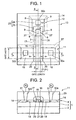
- FIG. 1 is an explanatory diagram showing an upper surface of a memory element according to a first embodiment
- FIG. 2 is an explanatory diagram illustrating a section taken along sectional line A-A of FIG. 1 ;
- FIG. 3 is an explanatory diagram showing a section taken along sectional line B-B of FIG. 1 ;
- FIG. 4 is an explanatory diagram depicting the state of setting of a region on an SOI layer employed in the first embodiment
- FIG. 5 is an explanatory diagram illustrating a method for manufacturing a semiconductor memory device according to the first embodiment
- FIG. 6 is an explanatory diagram showing the method for manufacturing the semiconductor memory device according to the first embodiment
- FIG. 7 is an explanatory diagram illustrating an erase operation of the memory element according to the first embodiment
- FIG. 8 is an explanatory diagram showing an upper surface of another form of the memory element according to the first embodiment.
- FIG. 9 is an explanatory diagram depicting an upper surface of a memory element according to a second embodiment.
- FIG. 1 is an explanatory diagram showing an upper surface of a memory element or device according to a first embodiment
- FIG. 2 is an explanatory diagram illustrating a section taken along sectional line A-A of FIG. 1
- FIG. 3 is an explanatory diagram showing a section taken along sectional line B-B of FIG. 1
- FIG. 4 is an explanatory diagram depicting the state of setting of a region on an SOI layer employed in the first embodiment
- FIGS. 5 and 6 are explanatory diagrams illustrating a method for manufacturing a semiconductor memory device according to the first embodiment
- FIG. 7 is an explanatory diagram illustrating an erase operation of the memory element according to the first embodiment.
- FIG. 1 is drawn in a state in which an interlayer insulating film and sidewalls are omitted.
- reference numeral 1 indicates a semiconductor substrate, which is a substrate of SOI structure formed by a support substrate 2 made up of silicon (Si), an embedded oxide film 3 used as an insulating film comprised of silicon oxide (SiO 2 ) of about 1500 ⁇ -thick formed on the support substrate 2 , and an SOI layer 4 used as a semiconductor layer comprised of monocrystalline silicon of an about 500 ⁇ -thick formed on the embedded oxide film 3 .
- MOS Metal Oxide Semiconductor
- the capacitor forming area 5 of the present embodiment is a polygon having five sharp edges or corners 9 , and is provided with a mountain portion 8 that protrudes toward the transistor forming area 6 , i.e., a pentagon.
- the capacitor forming area 5 and the transistor forming area 6 shown in FIG. 4 are respectively obtained by adding areas for forming slanting faces 27 (to be described later) to their peripheries in association with the form of the upper surface of the SOI layer 4 shown in FIG. 1 .
- An nMOS element 11 shown in FIG. 2 corresponding to a kind of MOSFET is formed in the transistor forming area 6 of the present embodiment.
- the MOS capacitor 12 shown in FIG. 3 is formed in the capacitor forming area 5 .
- the nMOS element 11 formed in the transistor forming area 6 and the MOS capacitor 12 formed in the capacitor forming area 5 are combined in series to form one memory or device 13 illustrated in FIG. 1 , which functions as an electrically reprogrammable one-bit non-volatile memory.
- Reference numeral 14 indicates a device isolation layer, which is an insulating layer that is provided in the SOI layer 4 of the device isolation area 7 and reaches the embedded oxide film 3 formed of an insulating material such as silicon oxide.
- the device isolation layer 14 has the function of electrically isolating and separating between the adjoining capacitor forming area 5 and transistor forming area 6 of the SOI layer 4 .
- Reference numeral 15 indicates a gate insulating film that is an insulating film of an about 50 to 150 ⁇ -thick made up of the insulating material such as silicon oxide, which is used commonly by the nMOS element 11 and the MOS capacitor 12 formed on the SOI layer 4 as shown in FIGS. 2 and 3 .
- Reference numeral 16 indicates a floating gate electrode that is an electrode comprising polysilicon or the like which is disposed opposite to the SOI layer 4 of the capacitor forming area 5 and the transistor forming area 6 with the gate insulating film 15 interposed therebetween. As shown in FIG. 1 , the floating gate electrode 16 is formed so as to extend from over a channel region 21 (to be described later) of the nMOS element 11 , which divides the transistor forming area 6 into two at its central portion, to over the corner 9 of the top of the mountain portion 8 on the transistor forming area 6 side lying on the capacitor forming area 5 .
- the floating gate electrode 16 functions as a gate electrode that the nMOS element 11 and the MOS capacitor 12 use in common.
- Sidewalls 17 made up of the insulating material such as silicon oxide or the like are formed on the side faces of the floating gate electrode 16 .
- the floating gate electrode 16 is brought to a floating state of being electrically insulated from outside by the gate oxide film 15 and the sidewalls 17 or the like.
- LDD (Lightly Doped Drain) portions 20 (N ⁇ ) of a source layer 18 and a drain layer 19 with a relatively low-concentration N-type impurity diffused therein are formed below the sidewalls 17 on the floating gate electrode 16 side at the source layer 18 and the drain layer 19 .
- Reference numeral 23 indicates a capacitor electrode, which comprises an N+ diffusion layer 24 formed by diffusing an impurity (N type in the present embodiment) of the same type as the source layer 18 into the SOI layer 4 of the capacitor forming area 5 in a relatively high concentration (over 1 ⁇ 10 18 ions/cm 3 , for example), and an N ⁇ diffusion layer 25 formed by diffusing an N-type impurity into the nMOS element 11 side in a relatively low concentration.
- the slanting faces 27 enlarged toward the embedded oxide film 3 are formed around the capacitor electrode 23 .
- An area for the corner 9 (corner 9 indicated by a broken line in FIG. 1 ) of the top of the mountain portion 8 including the slanting faces 27 on the nMOS element 11 side is disposed opposite to the floating gate electrode 16 via the gate insulating film 15 interposed therebetween.
- a tip or leading portion is formed in the area for the corner 9 opposite to the floating gate electrode 16 in a pointed state in pyramid form by the top of the mountain portion 8 and the slanting faces 27 lying on its side face side.
- This pyramidal tip is opposite to the floating gate electrode 16 via the gate insulating film 15 . Therefore, the concentration of an electric field becomes easy to occur in the pyramidal tip upon an erase operation of the memory element 13 to be described later.
- the pyramidal tip has the function of promoting the injection of charges into the floating gate electrode 16 .
- Reference numeral 28 indicates a capacitor trench or groove, which is a groove whose bottom face is formed within the embedded oxide film 3 by digging a slanting face 27 constituting a pyramidal tip of the capacitor electrode 23 formed below the floating gate electrode gate 16 and the device isolation layer 14 lying in an area adjacent to the slanting face 27 up to the embedded oxide film 3 and further digging the embedded oxide film 3 deeper than the thickness of the gate insulating film 15 .
- the length of the groove in a gate length direction is formed longer than the gate length of the floating gate electrode 16 shown in FIG. 1 .
- the capacitor groove 28 of the present embodiment is formed by digging the device isolation layer 14 lying below the floating gate electrodes 16 located between the N ⁇ diffusion layer 25 of the capacitor electrode 23 and the channel region 21 .
- Reference numeral 29 indicates an interlayer insulating film that is of an insulating film comprised of an insulating material such as silicon oxide, which covers the nMOS element 11 and the MOS capacitor 12 formed on the SOI layer 4 .
- Reference numerals 30 a through 30 c indicate contact plugs respectively, which are plugs formed by respectively embedding a conductive material such as tungsten (W) into contact holes 31 made open through the interlayer insulating film 29 as through holes that extend to over the source layer 18 and drain layer 19 of the nMOS element 11 and the N+ diffusion layer 24 of the capacitor electrode 23 of the MOS capacitor 12 .
- a conductive material such as tungsten (W)
- the contact plug 30 a connected to the source layer 18 of the nMOS element 11 is electrically connected to an unillustrated source line (SL) of the semiconductor memory device, which is formed of a wiring material relatively excellent in conductivity, such as aluminum (Al), copper (Cu) or the like
- SL source line
- the contact plug 30 b connected to the drain layer 19 of the nMOS element 11 is electrically connected to an unillustrated bit line (BL)
- the contact plug 30 c connected to the capacitor electrode 23 of the MOS capacitor 12 is electrically connected to an unillustrated word line (WL) as shown in FIG. 3 , respectively.
- An electrostatic capacitance C 1 (called electrostatic capacitance C 1 of MOS capacitor 12 and refer to FIG. 7 ) between the capacitor electrode 23 of the MOS capacitor 12 and the floating gate electrode 16 both employed in the present embodiment, and an electrostatic capacitance C 2 (called electrostatic capacitance C 2 on the source layer 18 side and refer to FIG. 7 ) between the source layer 18 and the floating gate electrode 16 of the nMOS element 11 are respectively set to take C 1 ⁇ C 2 by adjusting a capacitor area (called opposite area between the capacitor electrode 23 and the floating gate electrode 16 ), a MOSFET area (called opposite area between the source layer 18 and the floating gate electrode 16 ) or a gate width shown in FIG. 1 .
- reference numeral 41 indicates a resist mask, which is a mask member formed by performing exposure and development processing on a positive or negative resist applied onto the semiconductor substrate 1 by photolithography.
- the resist mask 41 functions as a mask used for etching and ion implantation in the present embodiment.
- Each of the slanting faces 27 of the capacitor electrode 23 can be formed using a birds beak having an approximately triangular sectional shape, which is formed by, when an SOI layer is oxidized with a silicon nitride film 44 used as an oxidation-resistant film located on a pad oxide film 43 (refer to FIG. 5 (P 3 )) as a mask by a LOCOS (Local Oxidation of Silicon) method thereby to form a device isolation layer 14 , intruding the tip or leading end of the device isolation layer 14 into a boundary portion between the silicon nitride film 44 and the SOI layer 4 in the capacitor forming area 5 .
- a birds beak having an approximately triangular sectional shape, which is formed by, when an SOI layer is oxidized with a silicon nitride film 44 used as an oxidation-resistant film located on a pad oxide film 43 (refer to FIG. 5 (P 3 )) as a mask by a LOCOS (Local Ox
- a method for manufacturing the semiconductor memory device of the present embodiment will be explained below in accordance with processes indicated by P in FIGS. 5 and 6 .
- FIGS. 5 and 6 are shown in section similar to the section shown in FIG. 3 .
- a pad oxide film 43 having a thin thickness is formed on the SOI layer 4 by a thermal oxidation method.
- a silicon nitride film 44 having a relatively thick thickness is formed on the pad oxide film 43 by a CVD (Chemical Vapor Deposition) method.
- a resist mask (not shown) which surrounds the capacitor forming area 5 and the transistor forming area 6 and exposes the silicon nitride film 44 of the device isolation area 7 , is formed on the silicon nitride film 44 by photolithography. With it as a mask, the silicon nitride film 44 and the pad oxide film 43 are etched by anisotropic etching to expose the SOI layer 4 and remove the resist mask.
- the SOI layer 4 is oxidized by the LOCOS method with the silicon nitride film 44 as a mask to form each device isolation layer 14 reaching the embedded oxide film 3 between the transistor forming area 6 and the capacitor forming area 5 .
- the silicon nitride film side of the SOI layer 4 is oxidized to form a birds beak, and slanting faces 27 enlarged toward the embedded oxide film 3 are formed around the SOI layer 4 in the transistor forming area 6 and the capacitor forming area 5 .
- the silicon nitride film 44 and the pad oxide film 43 are removed by wet etching using thermal phosphoric acid (Hot-H 2 PO 4 ) and hydrofluoric acid (HF) to expose the SOI layer 4 .
- thermal phosphoric acid Hot-H 2 PO 4
- HF hydrofluoric acid
- the device isolation layer 14 and the embedded oxide film 3 are etched by wet etching using hydrofluoric acid or the like to form a capacitor trench or groove 28 which has a bottom face within the embedded oxide film 3 and has exposed the slanting faces 27 .
- the length of the capacitor groove 28 in a gate length direction is formed longer than the gate length of the floating gate electrode 16 by anisotropy of wet etching. Further, a pyramidal tip or leading end formed by the slanting faces 27 and the corner 9 of the top of a mountain portion 8 is exposed in a state of being protruded within the capacitor groove 28 .
- the resist mask 41 formed at the process P 4 is removed, and a resist mask 41 that has exposed the SOI layer 4 of the capacitor forming area 5 is formed.
- a low-concentration N-type impurity is ion-implanted onto the SOI layer 4 to form a first N-type low-concentration diffusion layer 46 a for forming an N ⁇ diffusion layer 25 of a capacitor electrode 23 in the SOI layer 4 of the capacitor forming area 5 (first low-concentration N-type ion-implanting process step).
- the resist mask 41 formed at the process P 5 is removed, and a silicon oxide film comprised of silicon oxide for forming a gate insulating film 15 by a thermal oxidation method is formed over the SOI layer 4 and device isolation layer 14 in the capacitor forming area 5 and the transistor forming area 6 and at the internal surface of the capacitor groove 28 .
- a polysilicon film for forming the floating gate electrode 16 is deposited on the silicon oxide film by the CVD method.
- a resist mask (not shown) that covers the forming area of the floating gate electrode 16 , that is, a resist mask which divides the SOI layer 4 of the transistor forming area 6 into two and covers over the corner 9 (corner 9 indicated by the broken line, of the top of the mountain portion 8 shown in FIG. 1 in the present embodiment) of the top of the mountain portion 8 on the transistor forming area 6 side, of the SOI layer 4 of the capacitor forming area 5 is formed on the polysilicon film by photolithography.
- the polysilicon film and silicon oxide film exposed by anisotropic etching are etched to expose the SOI layer 4 , whereby a linear floating gate electrode 16 opposite to the SOI layer 4 of the transistor forming area 6 via the gate insulating film 15 and opposite to the pyramidal tip of the corner 9 on the transistor forming area 6 side, of the SOI layer 4 of the capacitor forming area 5 through the gate insulating film 15 is formed.
- the resist mask 41 is removed.
- a low-concentration N-type impurity is ion-implanted onto the SOI layer 4 in the transistor forming area 6 and the capacitor forming area 5 with the formed floating gate electrode 16 as a mask to form a second N-type low-concentration diffusion layer (not shown because it is formed in the transistor forming area 6 provided toward the front of the sheet and its depth direction in FIG. 6 ) for forming LDD portions 20 of a source layer 18 and a drain layer 19 at the SOI layer 4 lying on both sides of the floating gate electrode 16 (second low-concentration N-type ion-implanting process step).
- a silicon oxide film is formed on the floating gate electrode 16 and the SOI layer 4 , for example by the CVD method after the formation of the second N-type low-concentration diffusion layer.
- the entire surface lying above the SOI layer 4 is etched by anisotropic etching to expose the upper surface of the floating gate electrode 16 and the upper surface of the SOI layer 4 , after which sidewalls 17 are formed on their corresponding side faces of the floating gate electrode 16 .
- a high-concentration N-type impurity is ion-implanted onto the SOI layer 4 of the capacitor forming area 7 and the SOI layer 4 of the transistor forming area 6 by photolithography to form the source layer 18 and the drain layer 19 in the SOI layer 4 lying on both sides of the floating gate electrode 16 of the transistor forming area 6 and form an N+ diffusion layer 24 of the capacitor electrode 23 in an area uncovered with the flowing gate electrode 16 and the sidewalls 17 at the SOI layer 4 of the capacitor forming area 5 .
- an nMOS element 11 is formed in which the LDD portions 20 of the source layer 18 and drain layer 19 are formed below the sidewalls 17 located on the floating gate electrode 16 side, and a channel region 21 is formed below the floating gate electrode 16 disposed between the LDD portions 20 .
- a MOS capacitor 12 is formed in which the N ⁇ diffusion layer 25 with the N-type impurity diffused therein in the low concentration is formed below the floating gate electrode 16 and the sidewall 17 for the capacitor electrode 23 .
- a thick silicon oxide film is deposited on the SOI layer 4 containing over the nMOS element 11 , MOS capacitor 12 and device isolation layer 14 formed in this way, by the CVD method.
- the upper surface of the silicon oxide film is planarized or flattened to form an interlayer insulating film 29 .
- a resist mask (not shown) having exposed the interlayer insulating film 29 lying in forming areas of contact holes 31 located above the source layer 18 and drain layer 19 of the n MOS element 11 and the N+ diffusion layer 24 of the capacitor electrode 23 for the MOS capacitor 12 is formed on the interlayer insulating film 29 by photolithography. With it as a mask, the contact holes 31 which extend through the interlayer insulating film 29 and thereby reach the source layer 18 , drain layer 19 and capacitor electrode 23 , are formed by etching.
- the resist mask 41 is removed and a conductive material is embedded into the contact holes 31 by a sputtering method or the like to form contact plugs 30 a , 30 b and 30 c .
- Their upper surfaces are subjected to a planarization process to expose the upper surface of the interlayer insulating film 29 .
- a wiring layer comprised of a wiring material is formed on the interlayer insulating film 29 by the sputtering method or the like.
- the wiring layer is patterned by photolithography and etching to form a source line (SL) connected to the corresponding source layer 18 of the nMOS element 11 via the contact plug 30 a , a bit line (BL) connected to the corresponding drain layer 19 via the contact plug 30 b , and a word line (WL) connected to the corresponding capacitor electrode 23 of the MOS capacitor 12 via the contact plug 30 c , whereby a semiconductor memory device having the memory element 13 of the present embodiment shown in FIGS. 1 through 3 is formed.
- SL source line
- BL bit line
- WL word line
- the bit line (BL) connected to the drain layer 19 of the nMOS element 11 for forming the memory element 13 is brought to an open state (indicative of a state being nowhere to be electrically connected or a high impedance state), the word line (WL) connected to the capacitor electrode 23 of the MOS capacitor 12 is grounded (GND; 0V), and a voltage ranging from 10V to 15V is applied to the source line (SL) connected to the source layer 18 of the nMOS element 11 , as shown in FIG. 7 .
- the concentration of an electric field occurs in that portion and thereby the electric field applied to the MOS capacitor 12 is enhanced, so that an FN (Fowler Nordheim) tunnel current (called FN current) flows from the capacitor electrode 23 to the floating gate electrode 16 being held in a floating state, whereby electrons are easily injected into the floating gate electrode 16 .
- FN Fluler Nordheim tunnel current
- the electric charges are stored in the flowing gate electrode 16 in a short period of time.
- the threshold voltage of the nMOS element 11 rises and the threshold voltage of the memory element 13 is brought to a high state, i.e., an erase state.
- This state indicates a state in which “1” has been written into the memory element 13 as data.
- the erase state of the present embodiment corresponds to a state in which data “1” has been written into all memory elements 13 .
- each slanting face 27 is formed in the source layer 18 of the nMOS element 11 , the leading end or tip thereof is not opposite to the floating gate electrode 16 via the gate insulating film 15 . Therefore, no concentration of electric field occurs and no FN current flows through the gate insulating film 15 of the nMOS element 11 .
- the slanting faces 27 are formed using the birds beak formed when the device isolation layer 14 is formed by the LOCOS method in the present embodiment, the slanting faces 27 can easily be formed around the capacitor electrode 23 without adding a special process step.
- an electrically reprogrammable non-volatile memory can be formed in the semiconductor substrate 1 of SOI structure, thereby making it possible to miniaturize and thin the semiconductor memory device.
- an nMOS element and a polygonal MOS capacitor insulated and separated from each other by a device isolation layer are formed on an SOI layer of a semiconductor substrate of SOI structure. Slanting faces enlarged toward an embedded oxide film are provided around a capacitor electrode of the MOS capacitor.
- a floating gate electrode is provided which extends from over a channel region of a MOSFET to over the corner of an end portion on the nMOS element side, of the capacitor electrode and which is opposite to the channel region and the capacitor electrode with a gate insulating film interposed therebetween.
- the injection of electrons into the floating gate electrode can easily be done using the concentration of an electric field by a pyramidal tip or leading end formed at the corner below the floating gate electrode, of the capacitor electrode, regardless of a source-to-drain breakdown voltage. Even in a semiconductor memory device of SOI structure low in the source-to-drain breakdown voltage, the electric charges can be injected into the corresponding floating gate electrode in a short period of time, and an electrically reprogrammable non-volatile memory excellent in reliability can be formed.
- the slanting faces can easily be formed around the capacitor electrode using a birds beak formed when the device isolation layer is formed, without adding a special process.
- the capacitor forming area 5 is set to the polygon constituted by the pentagon, as shown in FIG. 8 , the capacitor forming area 5 is set to a polygon constituted by a rectangle having four corners 9 , whose one side is parallel to a rectangular transistor forming area 6 , and a floating gate electrode 16 shaped in a crank fashion may be extended on one corner 9 (corner 9 indicated by a left broken line in FIG. 8 in the present embodiment) lying on the nMOS element 11 side thereof.
- a pyramidal tip or leading end is formed by slanting faces 27 formed on both side faces of one corner 9 , and the injection of electrons into the corresponding floating gate electrode can easily be performed using the concentration of an electric field by the pyramidal tip formed at the corner below the floating gate electrode, of a capacitor electrode in a manner similar to the above.
- the capacitor groove 28 at the process P 4 ( FIG. 5 ) is formed in the following manner.
- the resist mask 41 for the capacitor groove 28 is set as a resist mask 41 having an opening that has exposed over the slanting faces 27 formed at one corner 9 of an SOI layer 4 lying below a forming area of the floating gate electrode 16 in its corresponding capacitor forming area 5 and that has exposed a device isolation layer 14 lying in an area adjacent to these slanting faces 27 .
- the device isolation layer 14 and its corresponding embedded oxide film 3 are etched by wet etching to form the corresponding capacitor groove 28 .
- the floating gate electrode 16 at the process P 6 is formed in the following manner.
- the resist mask 41 which covers the forming area of the floating gate electrode 16 is set as a resist mask 41 which divides the SOI layer 4 of the transistor forming area 6 into two and covers over one corner 9 (corner 9 indicated by the broken line in FIG. 8 in the present description) on the transistor forming area 6 side, of the SOI layer 4 of the capacitor forming area 5 .
- a polysilicon film and a silicon oxide film exposed by anisotropic etching are etched to expose the SOI layer 4 , whereby the corresponding floating gate electrode 16 is formed.
- crank-shaped floating gate electrode 16 is formed which is opposite to the SOI layer 4 of the transistor forming area 6 via the corresponding gate insulating film 15 and opposite to the pyramidal tip of one corner 9 of the SOI layer 4 of the capacitor forming area 5 through the gate insulating film 15 .
- FIG. 9 is an explanatory diagram showing an upper surface of a memory element or device according to a second embodiment.
- a capacitor forming area 5 is set to a polygon constituted by a rectangle having four corners 9 , whose one side is parallel to a rectangular transistor forming area 6 .
- a floating gate electrode 16 that extends in bent form is formed on both corners 9 on the nMOS element 11 side thereof.
- a width K at which the floating gate electrode 16 in this case and a capacitor electrode 23 overlap each other is set in such a manner that the width K is made relatively narrow and the width K is expanded to increase the area of an overlapping region, thereby giving high priority to elongating of the length of a slanting face 27 that exists in the overlapping region.
- a capacitor groove 28 employed in the present embodiment is formed in the following manner.
- the resist mask 41 thereat is set as a resist mask 41 having an opening that has exposed over the slanting faces 27 formed at both corners 9 of an SOI layer 4 lying below a forming area of the floating gate electrode 16 in its corresponding capacitor forming area 5 and that has exposed a device isolation layer 14 lying in an area adjacent to these slanting faces 27 .
- the device isolation layer 14 and its corresponding embedded oxide film 3 are etched by wet etching to form the corresponding capacitor groove 28 .
- the floating gate electrode 16 is formed in the following manner.
- the resist mask 41 which covers the forming area of the floating gate electrode 16 is set as a resist mask 41 which divides the SOI layer 4 of a transistor forming area 6 into two and covers over two corners 9 (two corners 9 indicated by broken lines in FIG. 9 in the present embodiment) on the transistor forming area 6 side, of the SOI layer 4 of a capacitor forming area 5 .
- a polysilicon film and a silicon oxide film exposed by anisotropic etching are etched to expose the SOI layer 4 , whereby the corresponding floating gate electrode 16 is formed.
- the bent floating gate electrode 16 is formed which is opposite to the SOI layer 4 of the transistor forming area 6 via the corresponding gate insulating film 15 and opposite to the two pyramidal tips of both corners 9 of the SOI layer 4 of the capacitor forming area 5 through the gate insulating film 15 .
- a floating gate electrode is formed so as to extend on both corners on the nMOS element side, of a capacitor electrode in addition to an effect similar to the first embodiment.
- slanting faces of the capacitor electrode opposite to the floating gate electrode can be elongated in a state including two pyramidal tips of both corners of the capacitor electrode.
- the amount of injection of electrons into the floating gate electrode at an erase operation can be increased using the concentration of an electric field by the two pyramidal tips formed at the corners on the floating gate electrode side, of the capacitor electrode, and a relatively long acute angle of each slanting face, and the injection of the electrons in the floating gate electrode can be performed in a shorter period of time.
- each of the embodiments has explained each of the transistors as the nMOS element, the embodiment is achieved in like manner even where the transistor is configured as a pMOS element and the type of impurity for both the capacitor electrode and high-concentration diffusion layer is made reverse.
Landscapes
- Engineering & Computer Science (AREA)
- Power Engineering (AREA)
- Microelectronics & Electronic Packaging (AREA)
- Physics & Mathematics (AREA)
- Condensed Matter Physics & Semiconductors (AREA)
- General Physics & Mathematics (AREA)
- Computer Hardware Design (AREA)
- Ceramic Engineering (AREA)
- Manufacturing & Machinery (AREA)
- Semiconductor Memories (AREA)
- Non-Volatile Memory (AREA)
- Thin Film Transistor (AREA)
Applications Claiming Priority (2)
| Application Number | Priority Date | Filing Date | Title |
|---|---|---|---|
| JP2007-144198 | 2007-05-30 | ||
| JP2007144198A JP2008300575A (ja) | 2007-05-30 | 2007-05-30 | 半導体記憶装置およびその製造方法 |
Publications (2)
| Publication Number | Publication Date |
|---|---|
| US20080296647A1 US20080296647A1 (en) | 2008-12-04 |
| US7807518B2 true US7807518B2 (en) | 2010-10-05 |
Family
ID=40087139
Family Applications (1)
| Application Number | Title | Priority Date | Filing Date |
|---|---|---|---|
| US12/081,633 Expired - Fee Related US7807518B2 (en) | 2007-05-30 | 2008-04-18 | Semiconductor memory device and manufacturing method thereof |
Country Status (2)
| Country | Link |
|---|---|
| US (1) | US7807518B2 (ja) |
| JP (1) | JP2008300575A (ja) |
Families Citing this family (4)
| Publication number | Priority date | Publication date | Assignee | Title |
|---|---|---|---|---|
| US8735906B2 (en) * | 2009-04-13 | 2014-05-27 | Rohm Co., Ltd. | Semiconductor device and method of manufacturing semiconductor device |
| US8395216B2 (en) * | 2009-10-16 | 2013-03-12 | Texas Instruments Incorporated | Method for using hybrid orientation technology (HOT) in conjunction with selective epitaxy to form semiconductor devices with regions of different electron and hole mobilities and related apparatus |
| US9431107B2 (en) | 2012-12-14 | 2016-08-30 | Taiwan Semiconductor Manufacturing Company, Ltd. | Memory devices and methods of manufacture thereof |
| CN109524457B (zh) * | 2017-09-20 | 2021-11-02 | 联华电子股份有限公司 | 半导体装置 |
Citations (4)
| Publication number | Priority date | Publication date | Assignee | Title |
|---|---|---|---|---|
| JP2001229690A (ja) | 2000-02-10 | 2001-08-24 | Hitachi Ltd | 半導体集積回路装置 |
| US20070187755A1 (en) * | 2006-02-10 | 2007-08-16 | Moore Paul M | Non-volatile memory cells and methods for fabricating the same |
| US20070228467A1 (en) * | 2006-03-31 | 2007-10-04 | Ikuo Kurachi | Semiconductor storage device and method of fabrication thereof |
| US20090065838A1 (en) * | 2007-09-12 | 2009-03-12 | Takeshi Nagao | Semiconductor memory device and method of manufacturing the same |
Family Cites Families (1)
| Publication number | Priority date | Publication date | Assignee | Title |
|---|---|---|---|---|
| JPH1187664A (ja) * | 1997-04-28 | 1999-03-30 | Nippon Steel Corp | 半導体装置及びその製造方法 |
-
2007
- 2007-05-30 JP JP2007144198A patent/JP2008300575A/ja active Pending
-
2008
- 2008-04-18 US US12/081,633 patent/US7807518B2/en not_active Expired - Fee Related
Patent Citations (5)
| Publication number | Priority date | Publication date | Assignee | Title |
|---|---|---|---|---|
| JP2001229690A (ja) | 2000-02-10 | 2001-08-24 | Hitachi Ltd | 半導体集積回路装置 |
| US6611458B2 (en) | 2000-02-10 | 2003-08-26 | Hitachi, Ltd. | Semiconductor integrated circuit device |
| US20070187755A1 (en) * | 2006-02-10 | 2007-08-16 | Moore Paul M | Non-volatile memory cells and methods for fabricating the same |
| US20070228467A1 (en) * | 2006-03-31 | 2007-10-04 | Ikuo Kurachi | Semiconductor storage device and method of fabrication thereof |
| US20090065838A1 (en) * | 2007-09-12 | 2009-03-12 | Takeshi Nagao | Semiconductor memory device and method of manufacturing the same |
Also Published As
| Publication number | Publication date |
|---|---|
| JP2008300575A (ja) | 2008-12-11 |
| US20080296647A1 (en) | 2008-12-04 |
Similar Documents
| Publication | Publication Date | Title |
|---|---|---|
| US7309634B2 (en) | Non-volatile semiconductor memory devices using prominences and trenches | |
| TWI393263B (zh) | 具有浮動閘、控制閘、選擇閘及具有在該浮動閘上方之突出部的抹除閘之改良分裂閘極非依電性快閃記憶體晶胞、陣列及製造方法 | |
| JP6094934B2 (ja) | デプレッションモード浮遊ゲートチャネルを備えた分割ゲートメモリセル、及びその製造方法 | |
| KR101347631B1 (ko) | 반도체 기억 장치 및 그 제조 방법 | |
| JP5289748B2 (ja) | 不揮発性半導体記憶装置、不揮発性半導体記憶装置の製造方法 | |
| US20080242026A1 (en) | Method of manufacturing a semiconductor memory device having a floating gate | |
| TWI433304B (zh) | 電子可抹除式唯讀記憶體單元 | |
| JP3113240B2 (ja) | 不揮発性半導体記憶装置とその製造方法 | |
| JP2001189439A (ja) | 不揮発性半導体記憶装置の製造方法及び不揮発性半導体記憶装置 | |
| US7807518B2 (en) | Semiconductor memory device and manufacturing method thereof | |
| JP4217409B2 (ja) | 不揮発性メモリ素子及びその製造方法 | |
| JP6298307B2 (ja) | 半導体メモリ装置およびその製造方法 | |
| US8198662B2 (en) | Semiconductor memory device and method of manufacturing the same | |
| JP2013168576A (ja) | 半導体装置および半導体装置の製造方法 | |
| JP2007287795A (ja) | 不揮発性半導体記憶装置 | |
| US8410537B2 (en) | Nonvolatile semiconductor memory device and method of manufacturing the same | |
| JP2011040626A (ja) | 半導体記憶装置及び半導体記憶装置の製造方法 | |
| JP5014591B2 (ja) | 半導体装置及びその製造方法 | |
| CN114335186A (zh) | 具有设置在字线栅上方的擦除栅的分裂栅非易失性存储器单元及其制备方法 | |
| TWI395323B (zh) | 半導體記憶體裝置及其製造方法 | |
| JP5982701B2 (ja) | 半導体装置および半導体装置の製造方法 | |
| JP2006041227A (ja) | 半導体装置およびその製造方法 | |
| KR100462370B1 (ko) | 플래쉬메모리장치및그의제조방법 | |
| JP5289422B2 (ja) | 半導体記憶装置およびその制御方法 | |
| JP2009049182A (ja) | 不揮発性半導体記憶素子 |
Legal Events
| Date | Code | Title | Description |
|---|---|---|---|
| AS | Assignment |
Owner name: OKI ELECTRIC INDUSTRY CO., LTD., JAPAN Free format text: ASSIGNMENT OF ASSIGNORS INTEREST;ASSIGNOR:TATSUMI, TOMOHIKO;REEL/FRAME:020891/0023 Effective date: 20080314 |
|
| AS | Assignment |
Owner name: OKI SEMICONDUCTOR CO., LTD., JAPAN Free format text: CHANGE OF NAME;ASSIGNOR:OKI ELECTRIC INDUSTRY CO., LTD.;REEL/FRAME:022162/0669 Effective date: 20081001 Owner name: OKI SEMICONDUCTOR CO., LTD.,JAPAN Free format text: CHANGE OF NAME;ASSIGNOR:OKI ELECTRIC INDUSTRY CO., LTD.;REEL/FRAME:022162/0669 Effective date: 20081001 |
|
| AS | Assignment |
Owner name: LAPIS SEMICONDUCTOR CO., LTD., JAPAN Free format text: CHANGE OF NAME;ASSIGNOR:OKI SEMICONDUCTOR CO., LTD;REEL/FRAME:032495/0483 Effective date: 20111003 |
|
| REMI | Maintenance fee reminder mailed | ||
| LAPS | Lapse for failure to pay maintenance fees | ||
| STCH | Information on status: patent discontinuation |
Free format text: PATENT EXPIRED DUE TO NONPAYMENT OF MAINTENANCE FEES UNDER 37 CFR 1.362 |
|
| FP | Lapsed due to failure to pay maintenance fee |
Effective date: 20141005 |