US7806496B2 - Printhead substrate, inkjet printhead, and inkjet printing apparatus - Google Patents
Printhead substrate, inkjet printhead, and inkjet printing apparatus Download PDFInfo
- Publication number
- US7806496B2 US7806496B2 US12/145,415 US14541508A US7806496B2 US 7806496 B2 US7806496 B2 US 7806496B2 US 14541508 A US14541508 A US 14541508A US 7806496 B2 US7806496 B2 US 7806496B2
- Authority
- US
- United States
- Prior art keywords
- power supply
- supply voltage
- circuit
- voltage
- printhead
- Prior art date
- Legal status (The legal status is an assumption and is not a legal conclusion. Google has not performed a legal analysis and makes no representation as to the accuracy of the status listed.)
- Expired - Fee Related, expires
Links
- 239000000758 substrate Substances 0.000 title claims description 49
- 238000007641 inkjet printing Methods 0.000 title claims description 5
- 230000003213 activating effect Effects 0.000 claims abstract description 6
- 239000007788 liquid Substances 0.000 claims description 2
- 230000007257 malfunction Effects 0.000 abstract 1
- 238000006243 chemical reaction Methods 0.000 description 20
- 238000010586 diagram Methods 0.000 description 14
- 238000007639 printing Methods 0.000 description 10
- 239000004065 semiconductor Substances 0.000 description 9
- 230000015556 catabolic process Effects 0.000 description 8
- 230000006870 function Effects 0.000 description 7
- 238000010248 power generation Methods 0.000 description 5
- 230000002159 abnormal effect Effects 0.000 description 4
- 239000003086 colorant Substances 0.000 description 2
- 229910044991 metal oxide Inorganic materials 0.000 description 2
- 150000004706 metal oxides Chemical class 0.000 description 2
- 230000002093 peripheral effect Effects 0.000 description 2
- XUIMIQQOPSSXEZ-UHFFFAOYSA-N Silicon Chemical compound [Si] XUIMIQQOPSSXEZ-UHFFFAOYSA-N 0.000 description 1
- 230000000295 complement effect Effects 0.000 description 1
- 230000007423 decrease Effects 0.000 description 1
- 238000000034 method Methods 0.000 description 1
- 238000012986 modification Methods 0.000 description 1
- 230000004048 modification Effects 0.000 description 1
- 229910052710 silicon Inorganic materials 0.000 description 1
- 239000010703 silicon Substances 0.000 description 1
- 238000000859 sublimation Methods 0.000 description 1
- 230000008022 sublimation Effects 0.000 description 1
- 230000001052 transient effect Effects 0.000 description 1
Images


Classifications
-
- B—PERFORMING OPERATIONS; TRANSPORTING
- B41—PRINTING; LINING MACHINES; TYPEWRITERS; STAMPS
- B41J—TYPEWRITERS; SELECTIVE PRINTING MECHANISMS, i.e. MECHANISMS PRINTING OTHERWISE THAN FROM A FORME; CORRECTION OF TYPOGRAPHICAL ERRORS
- B41J29/00—Details of, or accessories for, typewriters or selective printing mechanisms not otherwise provided for
- B41J29/38—Drives, motors, controls or automatic cut-off devices for the entire printing mechanism
-
- B—PERFORMING OPERATIONS; TRANSPORTING
- B41—PRINTING; LINING MACHINES; TYPEWRITERS; STAMPS
- B41J—TYPEWRITERS; SELECTIVE PRINTING MECHANISMS, i.e. MECHANISMS PRINTING OTHERWISE THAN FROM A FORME; CORRECTION OF TYPOGRAPHICAL ERRORS
- B41J2/00—Typewriters or selective printing mechanisms characterised by the printing or marking process for which they are designed
- B41J2/005—Typewriters or selective printing mechanisms characterised by the printing or marking process for which they are designed characterised by bringing liquid or particles selectively into contact with a printing material
- B41J2/01—Ink jet
- B41J2/015—Ink jet characterised by the jet generation process
- B41J2/04—Ink jet characterised by the jet generation process generating single droplets or particles on demand
- B41J2/045—Ink jet characterised by the jet generation process generating single droplets or particles on demand by pressure, e.g. electromechanical transducers
- B41J2/04501—Control methods or devices therefor, e.g. driver circuits, control circuits
- B41J2/04541—Specific driving circuit
-
- B—PERFORMING OPERATIONS; TRANSPORTING
- B41—PRINTING; LINING MACHINES; TYPEWRITERS; STAMPS
- B41J—TYPEWRITERS; SELECTIVE PRINTING MECHANISMS, i.e. MECHANISMS PRINTING OTHERWISE THAN FROM A FORME; CORRECTION OF TYPOGRAPHICAL ERRORS
- B41J2/00—Typewriters or selective printing mechanisms characterised by the printing or marking process for which they are designed
- B41J2/005—Typewriters or selective printing mechanisms characterised by the printing or marking process for which they are designed characterised by bringing liquid or particles selectively into contact with a printing material
- B41J2/01—Ink jet
- B41J2/015—Ink jet characterised by the jet generation process
- B41J2/04—Ink jet characterised by the jet generation process generating single droplets or particles on demand
- B41J2/045—Ink jet characterised by the jet generation process generating single droplets or particles on demand by pressure, e.g. electromechanical transducers
- B41J2/04501—Control methods or devices therefor, e.g. driver circuits, control circuits
- B41J2/04543—Block driving
-
- B—PERFORMING OPERATIONS; TRANSPORTING
- B41—PRINTING; LINING MACHINES; TYPEWRITERS; STAMPS
- B41J—TYPEWRITERS; SELECTIVE PRINTING MECHANISMS, i.e. MECHANISMS PRINTING OTHERWISE THAN FROM A FORME; CORRECTION OF TYPOGRAPHICAL ERRORS
- B41J2/00—Typewriters or selective printing mechanisms characterised by the printing or marking process for which they are designed
- B41J2/005—Typewriters or selective printing mechanisms characterised by the printing or marking process for which they are designed characterised by bringing liquid or particles selectively into contact with a printing material
- B41J2/01—Ink jet
- B41J2/015—Ink jet characterised by the jet generation process
- B41J2/04—Ink jet characterised by the jet generation process generating single droplets or particles on demand
- B41J2/045—Ink jet characterised by the jet generation process generating single droplets or particles on demand by pressure, e.g. electromechanical transducers
- B41J2/04501—Control methods or devices therefor, e.g. driver circuits, control circuits
- B41J2/0455—Details of switching sections of circuit, e.g. transistors
-
- B—PERFORMING OPERATIONS; TRANSPORTING
- B41—PRINTING; LINING MACHINES; TYPEWRITERS; STAMPS
- B41J—TYPEWRITERS; SELECTIVE PRINTING MECHANISMS, i.e. MECHANISMS PRINTING OTHERWISE THAN FROM A FORME; CORRECTION OF TYPOGRAPHICAL ERRORS
- B41J2/00—Typewriters or selective printing mechanisms characterised by the printing or marking process for which they are designed
- B41J2/005—Typewriters or selective printing mechanisms characterised by the printing or marking process for which they are designed characterised by bringing liquid or particles selectively into contact with a printing material
- B41J2/01—Ink jet
- B41J2/015—Ink jet characterised by the jet generation process
- B41J2/04—Ink jet characterised by the jet generation process generating single droplets or particles on demand
- B41J2/045—Ink jet characterised by the jet generation process generating single droplets or particles on demand by pressure, e.g. electromechanical transducers
- B41J2/04501—Control methods or devices therefor, e.g. driver circuits, control circuits
- B41J2/0458—Control methods or devices therefor, e.g. driver circuits, control circuits controlling heads based on heating elements forming bubbles
Definitions
- the present invention relates to inkjet printheads and printing apparatuses using the same. More particularly, the present invention relates to an inkjet printhead substrate on which electrothermal transducers for generating heat energy necessary for ejecting ink and drive circuits for driving the electrothermal transducers are formed, a printhead, and a printing apparatus using the printhead.
- electrothermal transducers (heaters) of a printhead mounted in an inkjet-based printing apparatus and drive circuits for driving the electrothermal transducers are formed on one and the same substrate using a semiconductor processing technique, as described in, for example, U.S. Pat. No. 6,290,334.
- a printing apparatus has a printhead in which an ink supplying port is provided near the center of a substrate, and heaters are provided at positions facing each other with the ink supplying port provided therebetween.
- FIG. 1 schematically illustrates circuit blocks and ink supplying ports of an inkjet printhead substrate (element substrate) 110 of this type.
- ink supplying ports 111 are formed on the element substrate 110 formed of semiconductor.
- a circuit block 115 including only one ink supplying port 111 at the left is illustrated, and circuit blocks 115 corresponding to the remaining five ink supplying slots 111 are only schematically illustrated.
- heaters 112 are arranged in an array at positions facing each other with the ink supplying port 111 provided therebetween.
- Drive circuits 113 for selecting and driving the corresponding heaters 112 are provided corresponding to the heaters 112 .
- Pads 114 for applying power and signals to the heaters 112 and the drive circuits 113 are arranged at edges of the element substrate 110 .
- FIG. 2 schematically illustrates the circuit structure of one drive circuit 113 shown in FIG. 1 and the flow of a signal.
- Data including image data applied to the pads 114 is connected to a shift register 204 and a decoder 205 included in an internal circuit via an input circuit 201 .
- the input data is applied as serial data, and the serial data is converted into parallel data by the shift register 204 .
- the image data included in the converted parallel data is input via a latch (not shown) to a plurality of heater driving blocks 206 (eight heater driving blocks 206 are arranged in this example).
- the shift register 204 has the function of a block selecting circuit 203 for selecting the validity/invalidity of the heater driving blocks 206 .
- Another portion of the converted parallel data is supplied to the decoder 205 disposed next to the shift register 204 .
- the decoder 205 has the function of a time-division selecting circuit 202 for outputting a time-division selection signal for sequentially selecting heaters driven in the heater driving blocks 206 .
- FIG. 3 is a circuit diagram of the interior of one heater driving block.
- a heater driving block 300 includes heater-driving metal-oxide semiconductor (MOS) transistors 305 , level conversion circuits 304 , and heater selecting circuits 305 , which are arranged corresponding to heaters 306 arranged in an array.
- a heater power supply voltage (first power supply voltage) is applied from the outside to heater power supply lines 301 .
- the heater-driving MOS transistors 305 perform the function of a switch for allowing or preventing the flow of current to the corresponding heaters 306 .
- a block selection signal 302 and a time-division signal 303 are input to an AND gate serving as each of the heater selecting circuits 305 . When these two signals become active, the output of the AND gate becomes active.
- the voltage amplitude of an output signal of the AND gate is converted by a corresponding one of the level conversion circuits 304 to a power supply voltage (second power supply voltage) that is higher than a drive voltage (third power supply voltage) at a level of a logic circuit including the input circuit and a corresponding one of the heater selecting circuits 305 .
- the level-converted signal is applied to the gate of a corresponding one of the heater-driving MOS transistors 305 .
- the voltage amplitude of the output signal is converted to the higher second power supply voltage because of the following reason.
- the on-resistance of the heater-driving MOS transistor 305 is reduced. Accordingly, current can more efficiently flow through the heater 306 .
- the voltage value of the second power supply voltage should not exceed a circuit breakdown voltage and a gate breakdown voltage of the MOS, and the second power supply voltage should be set to as high a value as possible. Further, if possible, the voltage value of the second power supply voltage may be the same as the voltage value of the first power supply voltage, which is the voltage value of the heater power supply lines 301 . In most cases, however, the power supply voltage applied to heaters is generally set to a relatively high value, such as 20 V or greater. In most cases, a complementary metal-oxide semiconductor (CMOS) inverter is generally processed to have a breakdown voltage of about 15 V.
- CMOS complementary metal-oxide semiconductor
- a power generation circuit for generating a desired second power supply voltage from a heater power supply voltage (first power supply voltage) is provided in the interior of a printhead substrate.
- first power supply voltage first power supply voltage
- U.S. Pat. No. 6,712,437 describes an example of a circuit in which an input voltage VDD for a logic circuit is input to a heater-driving switching element.
- VDD heater power supply voltage
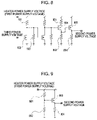
- FIG. 9 illustrates an example of a power generation circuit.
- the circuit shown in this example includes an nMOS transistor 803 and a resistor 804 constituting an nMOS source follower, and resistor dividers 801 and 802 .
- the heater power supply voltage (first power supply voltage) is divided by the resistor dividers 801 and 802 , and the divided voltage is applied to the gate of the nMOS transistor 803 .
- An output of the source follower serves as the second power supply voltage.
- the resistor dividers 801 and 802 the voltage applied to the gate of the nMOS transistor 803 can be set to a desired value. Accordingly, the second power supply voltage can be a voltage that is lower than the heater power supply voltage (first power supply voltage).
- FIG. 5 is a circuit diagram of the internal structure of a level conversion circuit and its peripheral circuits.
- a heater-driving MOS transistor 505 a heater-driving MOS transistor 505 , a heater 506 , a PMOS transistor 510 , and an NMOS transistor 511 are shown.
- a signal supplied from a heater selecting circuit is inverted by an inverter operating at the third power supply voltage to generate an inverted logic signal, and this generated signal is applied to the gate of an NMOS transistor and a PMOS transistor operating at the second power supply voltage.
- the transistors driven by the second power supply voltage need to be elements that can withstand the second power supply voltage.
- FIG. 4 is a circuit block diagram of the structure in which level conversion is performed immediately after a shift register and a decoder.
- pads 401 , a time-division selecting circuit 402 , and a block selecting circuit 403 are shown.
- the point that is different from the foregoing circuit structure is that output signals of a shift register 404 and a decoder 405 are level-converted by level conversion circuits 411 and 412 , respectively.
- Circuits driven by the third power supply voltage, which has the same voltage amplitude and the same potential as an input signal, are those enclosed by line 415 .
- Circuit blocks driven by the second power supply voltage higher than the level-converted first power supply voltage are those enclosed by line 416 .
- These circuit blocks enclosed by line 416 include heater driving blocks 406 .
- the third power supply voltage which has the voltage amplitude of an input signal and which activates logic circuit blocks is used. Further, the higher second power supply voltage applied to the gate of a MOS transistor, which is a switching element for controlling heater current, is used. The circuits are controlled and driven by these two power supply voltages. Further, an output signal of a drive circuit for supplying the third power supply voltage is converted by a level conversion circuit into a signal with the signal amplitude of the second power supply voltage.
- the first and third power supply voltages are supplied from a printer body to the printhead semiconductor substrate.
- the second power supply voltage is generated by converting the first power supply voltage via a power supply voltage generation circuit provided in the substrate to a voltage lower than the first power supply voltage.
- the sequence of supplying these voltages to the printhead semiconductor substrate is such that, after the third power supply voltage is applied, the heater power supply voltage (first power supply voltage) is applied. This is because, if the heater power supply voltage (first power supply voltage) is applied in a state where no third power supply voltage is applied, the head may operate unexpectedly.
- the heater driving circuit including the level conversion circuit is enabled.
- an input signal of the level conversion circuit is output from a circuit that operates based on the third power supply voltage.
- the logic thereof becomes indefinite. In this state, the logic of an output of the level conversion circuit becomes indefinite, which may result in the logic where an unexpected heater is turned on.
- the present invention provides a printhead substrate, an inkjet printhead, and an inkjet printing apparatus for preventing the flow of heater current due to an indefinite logic state even when a second power supply voltage and/or a heater power supply voltage (first power supply voltage) is applied prior to a third power supply voltage.
- a printhead substrate including an electrothermal transducer configured to eject liquid and a drive circuit including a switching element configured to drive the electrothermal transducer.
- the drive circuit includes a logic circuit configured to control driving of the electrothermal transducer, and a power supply voltage generation circuit configured to generate, from a first power supply voltage applied to the electrothermal transducer, a second power supply voltage for activating the switching element based on a voltage value of a third power supply voltage for activating the logic circuit.
- the second power supply voltage for driving the switching element is generated from the first power supply voltage.
- the switching element is not driven by the second power supply voltage.
- FIG. 1 schematically illustrates circuit blocks and ink supplying ports provided on an inkjet printhead semiconductor substrate.
- FIG. 2 schematically illustrates the circuit structure of a drive circuit shown in FIG. 1 and the flow of a signal.
- FIG. 3 is a circuit diagram of the interior of a heater driving block in a known example.
- FIG. 4 is a circuit block diagram of the structure in which level conversion is performed immediately after a shift register and a decoder in a known example.
- FIG. 5 is a circuit diagram of the internal structure of a level conversion circuit and its peripheral circuits.
- FIG. 6 is a circuit diagram of a second power supply voltage generation circuit for describing a first exemplary embodiment of the present invention.
- FIG. 7 is a circuit diagram of a second power supply voltage generation circuit for describing a second exemplary embodiment of the present invention.
- FIG. 8 is a circuit diagram of a second power supply voltage generation circuit for describing another example of the circuit structure according to an embodiment of the present invention.
- FIG. 9 is a circuit diagram of an example of a power generation circuit.
- FIG. 10 is a perspective view of a three-dimensional structure of a printhead IJHC for ejecting three colors of color ink.
- FIG. 11 is an external view of a printing apparatus applicable to an embodiment of the present invention.
- FIG. 12 is a block diagram of a control structure of the printing apparatus.
- FIG. 13 schematically illustrates a printhead substrate according to an embodiment of the present invention.
- element substrate used in the description does not refer to a simple substrate made of silicon semiconductor, but refers to a substrate on which elements and wiring lines are provided.
- on the element substrate does not simply refer to being on the surface of the element substrate, but also refers to being on the surface of the substrate and being inside the element substrate, near the surface thereof.
- print element refers to, in the case of an inkjet print system, a structure including an ejection energy generating element for generating ejection energy for ejecting ink, an ejection port, and a channel.
- FIG. 6 is a circuit diagram of, in a circuit structure inside an element substrate, a second power supply voltage generation circuit for describing a first exemplary embodiment of the present invention.
- the second power supply voltage generation circuit generates a second power supply voltage from a first power supply voltage serving as a heater power supply voltage.
- FIG. 13 schematically illustrates a printhead substrate according to an embodiment of the present invention.
- a printhead substrate 33 includes a heater 31 serving as an electrothermal transducer, a VH which is a first power supply line for supplying power to the heater 31 , a switching element 32 for driving the heater 31 , and a logic circuit for controlling driving of the heater 31 .
- the logic circuit is, as shown in FIG. 13 , a circuit including a shift register and a latch circuit.
- a third power supply voltage VDD is input to the logic circuit.
- a second power supply voltage for activating the switching element 32 is a power supply voltage input to the switching element 32 shown in FIG. 13 .
- the second power supply voltage may be, on the printhead substrate 33 shown in FIG. 13 , a voltage output from a level converter and input to the switching element 32 .
- the second power supply voltage may be provided through a power supply line VHT for driving the switching element 32 in FIG. 13 .
- an nMOS transistor 803 and a resistor 804 constituting an nMOS source follower, and resistor dividers 801 and 802 are similar to those of a voltage generation circuit illustrated in the known example shown in FIG. 9 .
- a resistor 101 , an nMOS transistor 102 , a resistor 103 , and an nMOS transistor 104 constitute an additional circuit according to an embodiment of the present invention. With this additional circuit, turning on and off of a voltage supplying circuit is controlled.
- the resistor 101 and the nMOS transistor 102 constitute a first inverter circuit operating at the heater power supply voltage.
- the third power supply voltage is applied to the gate of the nMOS transistor 102 serving as an input of the first inverter circuit.
- An output of the first inverter circuit is connected to the gate of the nMOS transistor 104 .
- the heater power supply voltage is a voltage applied to an electrothermal transducer (heater), as has been described above. In recent years, this voltage has been about 24 V. In the element substrate, this voltage is higher than other voltages.
- the third power supply voltage is a power supply voltage for driving the logic circuit including the shift register 204 and the decoder 205 , which have been described using FIG. 2 , for controlling driving of electrothermal transducers.
- a voltage of about 3.3 V is used as the third power supply voltage.
- a latch circuit may be provided at the subsequent stage of the shift register 204 . The latch circuit is also driven by the third power supply voltage.
- the resistor 103 is a resistor divider connected so that the voltage applied to the gate of a corresponding nMOS transistor does not exceed a gate breakdown voltage when the first inverter circuit is turned off.
- the resistor 103 must have a resistance value such that, when the nMOS transistor 102 is turned off, a divided voltage value obtained in conjunction with the resistor 101 is greater than or equal to a threshold voltage of the nMOS transistor 104 and less than the gate breakdown voltage of the nMOS transistor 104 .
- the resistor 103 is unnecessary when the gate breakdown voltage of the nMOS transistor 104 is greater than or equal to the heater power supply voltage.
- the nMOS transistor 104 constitutes, together with the resistor divider 801 of the voltage supplying circuit, a second inverter circuit. That is, the resistor divider 801 plays both the function of the resistor divider of the voltage supplying circuit and the function in the second inverter circuit.
- An output of the second inverter circuit is connected to the gate of the nMOS transistor 803 constituting the nMOS source follower circuit.
- the output of the first inverter circuit is substantially 0 V. Therefore, the nMOS transistor 104 included in the second inverter circuit is turned off, and the power supply voltage generation circuit is in an operating state similar to that of the circuit of the known example.
- the output of the first inverter circuit is a divided voltage value obtained by the resistor 101 and the resistor 103 . Since a voltage obtained from the divided voltage obtained by the resistor 101 and the resistor 103 is set to be greater than or equal to the threshold of the nMOS transistor 104 , the nMOS transistor 104 is turned on. In this state, the gate voltage of the nMOS transistor 803 , which is the output of the second inverter circuit, is substantially 0 V, and the nMOS transistor 803 is turned off. Since the nMOS transistor 803 is turned off, the output of the second power supply voltage is fixed to 0 V.
- the second power supply voltage is a voltage applied to a heater-driving MOS transistor (switching element), which is a switch for allowing or preventing the flow of current to a corresponding electrothermal transducer (see FIGS. 3 , 5 , and 12 ).
- switching element switching element
- the third power supply voltage when the third power supply voltage is properly applied, the second power supply voltage is supplied. In contrast, when the third power supply voltage is not properly applied, the second power supply voltage is not supplied, resulting in 0 V.
- the output of the heater driving circuit becomes 0 V. That is, when the second power supply voltage is 0 V, no abnormal current is allowed to flow through the heater due to an indefinite logic state.
- the second power supply voltage is output or not depends on whether the third power supply voltage is greater than or equal to or less than the threshold voltage of the nMOS transistor 102 . If the nMOS transistor 102 has the same structure as an nMOS transistor which is included in the level conversion circuit shown in FIG. 5 and which is driven by the second power supply voltage, the threshold of the power supplying circuit can be substantially equivalent to the threshold of the level conversion circuit. Accordingly, an indefinite logic state due to application of the third power supply voltage less than the threshold of the level conversion circuit can be avoided.
- FIG. 7 is a circuit diagram of a second power supply voltage generation circuit for describing a second exemplary embodiment of the present invention.
- the second power supply voltage generation circuit according to the second exemplary embodiment has a feature that an nMOS transistor 105 is added to a second power supply voltage node.
- the nMOS transistor 105 is turned off when the output of the second power supply voltage is valid and turned on when the output of the second power supply voltage is invalid, the nMOS transistor 105 is connected so that the gate of the nMOS transistor 105 is parallel to the gate of the nMOS transistor 104 .
- the nMOS transistor 105 is disposed in order to function as a current path for causing the second power supply voltage to quickly converge to 0 V when the second power supply voltage generation circuit which has been turned on is turned off.
- circuits constituting level conversion circuits and the like are connected to the second power supply voltage. Elements constituting these circuits have capacitive components. These capacitive components accumulate electric charge when the output of the second power supply voltage is valid. Now, suppose that the supply of the third power supply voltage which has been properly applied is unexpectedly stopped due to a certain reason.
- the source follower nMOS transistor 803 When there is no nMOS transistor 105 , the source follower nMOS transistor 803 is turned off. No electric charge is supplied to the second power supply voltage. Electric charge in the second power supply voltage line is discharged to ground GND via the resistor 804 .
- the resistor 804 is a resistor included in the nMOS source follower circuit. In most cases, the resistor 804 is set to a high resistance value of about a few tens of k ⁇ to a few hundreds of k ⁇ . When many elements are connected to the second power supply voltage and the capacitance of the second power supply line is large, a time constant based on the capacitance and the resistor 804 becomes large. When the power supplying circuit which has been turned on is now turned off, regardless of the fact that the third power supply voltage has a value based on which the logic cannot be determined, due to the remaining electric charge in the second power supply voltage line, the circuits which are connected to the second power supply voltage and which remain in the indefinite logic state may start operating.
- the present embodiment provides a structure for avoiding maintaining such a transient indefinite logic state.
- the nMOS transistor 105 is disposed so as to bypass the source follower resistor 804 . Accordingly, when the power supplying circuit which has been turned on is now turned off, the remaining electric charge in the second power supply voltage line can be quickly discharged, and the supply of the second power supply voltage to circuits that operate based on the second power supply voltage can be cut off.
- the output of the first inverter circuit becomes a divided voltage value obtained by the resistor 101 and the resistor 103 .
- a voltage obtained from the divided voltage obtained by the resistor 101 and the resistor 103 is set to be greater than or equal to a threshold of the nMOS transistor 105 .
- the nMOS transistor 104 is turned on.
- the gate voltage of the nMOS transistor 803 which is the output of the second inverter circuit, is substantially 0 V, and the nMOS transistor 803 is turned off. Since the nMOS transistor 105 is turned on, the electric charge accumulated in the second power supply voltage line is discharged to ground GND, and the second power supply voltage quickly converges to 0 V.
- the description assumes that the first power supply voltage is applied from the outside to the printhead substrate.
- a power generation circuit may be provided on the printhead substrate, and the power generation circuit may generate the third power supply voltage from the heater power supply voltage and supply the generated third power supply voltage to the interior of the substrate.
- the third power supply voltage generation circuit is provided inside the substrate, it becomes unnecessary to supply power supply voltages from a printer body to the substrate. Accordingly, the number of connection terminals can be reduced, and a power supply circuit of the printer body can be further simplified. In this case, the flow of abnormal current due to an indefinite logic state can be avoided by causing the output of the second power supply voltage generation circuit to become valid after the output voltage (third power supply voltage) of the third power supply voltage generation circuit in the printhead substrate becomes stable.
- whether to turn on and off the supply of the second power supply voltage is determined by the value of the third power supply voltage.
- this determination can be made by a signal indicating the state of the head or the printer body.
- power or a signal for making the determination may be applied as current.
- an nMOS transistor 904 may be connected in series between the resistors 801 and 802 , and a node between the nMOS transistor 904 and the resistor 802 may be connected to the gate of the nMOS transistor 803 .
- FIG. 8 In the structure shown in FIG.
- the nMOS transistor 904 when the output is valid, the nMOS transistor 904 is turned on, and a divided voltage obtained from the sum voltage of the resistor 801 and the nMOS transistor 904 and the voltage of the resistor 802 is applied to the gate of the nMOS transistor 803 , thereby outputting the second power supply voltage.
- the gate voltage of the nMOS transistor 904 becomes GND potential, and the nMOS transistor 904 is turned off. Accordingly, the gate voltage of the nMOS transistor 804 becomes GND potential, and the second power supply voltage becomes 0 V.
- the present invention can be achieved using various circuit structures other than those described above.
- a common feature of the circuit structures is that the output of the second power supply voltage generation circuit is controlled according to the state of the third power supply voltage. That is, turning on (valid) and off (invalid) the output of the second power supply voltage generation circuit is controlled according to whether the output of circuits operating at the third power supply voltage can control the level conversion circuit operating at the second power supply voltage.
- the output of the second power supply voltage generation circuit is fixed to 0 V. Accordingly, no unexpected heaters are selected and driven.
- FIG. 10 is a perspective view of a three-dimensional structure of a printhead for ejecting three colors of color ink.
- the printhead includes ink supplying ports 2 C, 2 M, and 2 Y for supplying cyan (C), magenta (M), and yellow (Y) ink, respectively.
- Ink channels 301 C, 301 M, and 301 Y are provided corresponding to electrothermal transducers (heaters) 121 .
- C ink, M ink, and Y ink are directed via these ink channels 301 C, 301 M, and 301 Y to the electrothermal transducers (heaters) 121 provided on an element substrate 110 .
- the electrothermal transducers (heaters) 121 are driven, the ink boils, and bubbles are generated. With the generated bubbles, ink droplets 900 C, 900 M, and 900 Y are ejected through ejection ports 302 C, 302 M, and 302 Y provided for the corresponding electrothermal transducers (heaters) 121 .
- the electrothermal transducers (heaters) 121 , drive circuits, and pads, which have been described above, are formed on the element substrate 110 .
- a printhead IJHK for ejecting black ink has a similar structure.
- the structure of the printhead IJHK for ejecting black ink is one-third of the structure shown in FIG. 10 . That is, the structure has only one ink supplying port.
- the size of an element substrate of the printhead IJHK is about one-third the size of the element substrate 110 shown in FIG. 10 .
- FIG. 11 is an external view of a typical inkjet printing apparatus IJPA according to an embodiment of the present invention.
- a carriage HC has a pin (not shown) that engages with a spiral groove 5005 of a lead screw 5004 .
- the carriage HC which is supported by a guide rail 5003 , reciprocates in the directions a and b indicated by arrows in accordance with the rotation of the lead screw 5004 .
- the carriage HC has an inkjet cartridge IJC.
- the inkjet cartridge IJC has an inkjet printhead IJH (hereinafter referred to as a “printhead”) and an ink tank IT for storing print ink.
- the inkjet cartridge IJC includes the printhead IJH and the ink tank IT, which are integrated with each other.
- a platen 5000 is rotated by a convey motor (not shown) and conveys print paper P.
- FIG. 12 is a block diagram of a control structure of the printing apparatus.
- the control structure includes an interface 1700 for receiving a print signal, a microprocessing unit (MPU) 1701 , a read-only memory (ROM) 1702 for storing a control program executed by the MPU 1701 , a dynamic random access memory (DRAM) 1703 for storing various items of data (print data supplied to the foregoing printhead IJH, or the like), and a gate array (GA) 1704 for controlling the supply of print data to the printhead IJH.
- the GA 1704 controls data transfer among the interface 1700 , the MPU 1701 , and the RAM 1703 .
- control structure includes a convey motor 1709 (which has not been shown in FIG. 11 ) for conveying print paper P, a motor driver 1706 for driving the convey motor 1709 , a motor driver 1707 for driving a carriage motor 1710 , and a head driver (driver circuit) 1705 for driving the printhead IJH.
- the head driver 1705 outputs data including image data, time-division data, and identification data and the above-described first and third power supply voltages to the printhead IJH.
- the inkjet printhead using the electrothermal transducers (heaters) as ejection energy generating elements constituting print elements has been described by way of example.
- the present invention is also applicable to an inkjet printhead using piezoelectric elements as ejection energy generating elements or a thermal head that can be used in a dye sublimation type or the like.
Landscapes
- Engineering & Computer Science (AREA)
- Microelectronics & Electronic Packaging (AREA)
- Particle Formation And Scattering Control In Inkjet Printers (AREA)
Priority Applications (1)
| Application Number | Priority Date | Filing Date | Title |
|---|---|---|---|
| US12/861,677 US8038238B2 (en) | 2007-06-26 | 2010-08-23 | Printhead substrate, inkjet printhead, and inkjet printing apparatus |
Applications Claiming Priority (2)
| Application Number | Priority Date | Filing Date | Title |
|---|---|---|---|
| JP2007167456 | 2007-06-26 | ||
| JP2007-167456 | 2007-06-26 |
Related Child Applications (1)
| Application Number | Title | Priority Date | Filing Date |
|---|---|---|---|
| US12/861,677 Continuation US8038238B2 (en) | 2007-06-26 | 2010-08-23 | Printhead substrate, inkjet printhead, and inkjet printing apparatus |
Publications (2)
| Publication Number | Publication Date |
|---|---|
| US20090002457A1 US20090002457A1 (en) | 2009-01-01 |
| US7806496B2 true US7806496B2 (en) | 2010-10-05 |
Family
ID=40159879
Family Applications (2)
| Application Number | Title | Priority Date | Filing Date |
|---|---|---|---|
| US12/145,415 Expired - Fee Related US7806496B2 (en) | 2007-06-26 | 2008-06-24 | Printhead substrate, inkjet printhead, and inkjet printing apparatus |
| US12/861,677 Expired - Fee Related US8038238B2 (en) | 2007-06-26 | 2010-08-23 | Printhead substrate, inkjet printhead, and inkjet printing apparatus |
Family Applications After (1)
| Application Number | Title | Priority Date | Filing Date |
|---|---|---|---|
| US12/861,677 Expired - Fee Related US8038238B2 (en) | 2007-06-26 | 2010-08-23 | Printhead substrate, inkjet printhead, and inkjet printing apparatus |
Country Status (2)
| Country | Link |
|---|---|
| US (2) | US7806496B2 (enExample) |
| JP (1) | JP4995150B2 (enExample) |
Cited By (2)
| Publication number | Priority date | Publication date | Assignee | Title |
|---|---|---|---|---|
| US20090135229A1 (en) * | 2007-11-27 | 2009-05-28 | Canon Kabushiki Kaisha | Element substrate, printhead, and head cartridge |
| US20100134543A1 (en) * | 2008-12-01 | 2010-06-03 | Canon Kabushiki Kaisha | Recording element substrate and recording head having the same |
Families Citing this family (9)
| Publication number | Priority date | Publication date | Assignee | Title |
|---|---|---|---|---|
| JP5909049B2 (ja) | 2011-03-31 | 2016-04-26 | キヤノン株式会社 | 液体吐出ヘッドおよび液体吐出装置 |
| JP6222998B2 (ja) * | 2013-05-31 | 2017-11-01 | キヤノン株式会社 | 素子基板、フルライン記録ヘッド及び記録装置 |
| JP6148562B2 (ja) | 2013-07-26 | 2017-06-14 | キヤノン株式会社 | 基板、記録ヘッド及び記録装置 |
| JP6126489B2 (ja) * | 2013-07-29 | 2017-05-10 | キヤノン株式会社 | 記録素子基板、記録ヘッド及び記録装置 |
| WO2016068849A1 (en) * | 2014-10-27 | 2016-05-06 | Hewlett-Packard Development Company, L.P. | Printing device |
| JP6307469B2 (ja) * | 2015-04-10 | 2018-04-04 | 株式会社東芝 | インクジェットプリンタ |
| JP6387955B2 (ja) * | 2015-12-25 | 2018-09-12 | セイコーエプソン株式会社 | ヘッドユニット制御回路 |
| JP6701723B2 (ja) * | 2015-12-25 | 2020-05-27 | セイコーエプソン株式会社 | 接続ケーブル |
| JP6769200B2 (ja) * | 2016-09-16 | 2020-10-14 | ブラザー工業株式会社 | 制御基板、印刷装置及びヘッドモジュール |
Citations (6)
| Publication number | Priority date | Publication date | Assignee | Title |
|---|---|---|---|---|
| US5083137A (en) * | 1991-02-08 | 1992-01-21 | Hewlett-Packard Company | Energy control circuit for a thermal ink-jet printhead |
| JPH11129479A (ja) | 1997-10-31 | 1999-05-18 | Canon Inc | 記録ヘッド及び該記録ヘッドを用いた記録装置 |
| US6290334B1 (en) | 1991-08-02 | 2001-09-18 | Canon Kabushiki Kaisha | Recording apparatus, recording head and substrate therefor |
| US6302504B1 (en) * | 1996-06-26 | 2001-10-16 | Canon Kabushiki Kaisha | Recording head and recording apparatus using the same |
| US6712437B2 (en) | 2001-06-15 | 2004-03-30 | Canon Kabushiki Kaisha | Printhead board, printhead and printing apparatus |
| US6971735B2 (en) | 2001-06-15 | 2005-12-06 | Canon Kabushiki Kaisha | Ink-jet printhead board, ink-jet printhead, and ink-jet printing apparatus |
Family Cites Families (10)
| Publication number | Priority date | Publication date | Assignee | Title |
|---|---|---|---|---|
| JPH09174832A (ja) * | 1995-12-27 | 1997-07-08 | Brother Ind Ltd | 印字装置 |
| JP3082661B2 (ja) * | 1996-03-21 | 2000-08-28 | 富士ゼロックス株式会社 | インクジェット記録装置 |
| JP3327791B2 (ja) * | 1996-11-12 | 2002-09-24 | キヤノン株式会社 | 記録ヘッド及びその記録ヘッドを用いた記録装置 |
| JP2000141660A (ja) * | 1998-11-11 | 2000-05-23 | Canon Inc | 記録へッド及びその記録へッドを用いた記録装置 |
| JP2000198198A (ja) * | 1999-01-05 | 2000-07-18 | Fuji Xerox Co Ltd | 液体噴射記録装置 |
| JP4261874B2 (ja) * | 2002-11-01 | 2009-04-30 | キヤノン株式会社 | 記録ヘッドおよび記録装置 |
| JP4532890B2 (ja) * | 2003-12-11 | 2010-08-25 | キヤノン株式会社 | 記録ヘッドおよび該記録ヘッドを備えた記録装置 |
| JP4208770B2 (ja) * | 2004-06-10 | 2009-01-14 | キヤノン株式会社 | 記録ヘッド及び該記録ヘッドが用いられる記録装置 |
| JP4678825B2 (ja) * | 2004-12-09 | 2011-04-27 | キヤノン株式会社 | ヘッド基板、記録ヘッド、ヘッドカートリッジ、及びその記録ヘッド或いはヘッドカートリッジを用いた記録装置 |
| JP4859213B2 (ja) * | 2005-06-16 | 2012-01-25 | キヤノン株式会社 | 記録ヘッドの素子基体、記録ヘッド、記録装置 |
-
2008
- 2008-06-18 JP JP2008159316A patent/JP4995150B2/ja not_active Expired - Fee Related
- 2008-06-24 US US12/145,415 patent/US7806496B2/en not_active Expired - Fee Related
-
2010
- 2010-08-23 US US12/861,677 patent/US8038238B2/en not_active Expired - Fee Related
Patent Citations (6)
| Publication number | Priority date | Publication date | Assignee | Title |
|---|---|---|---|---|
| US5083137A (en) * | 1991-02-08 | 1992-01-21 | Hewlett-Packard Company | Energy control circuit for a thermal ink-jet printhead |
| US6290334B1 (en) | 1991-08-02 | 2001-09-18 | Canon Kabushiki Kaisha | Recording apparatus, recording head and substrate therefor |
| US6302504B1 (en) * | 1996-06-26 | 2001-10-16 | Canon Kabushiki Kaisha | Recording head and recording apparatus using the same |
| JPH11129479A (ja) | 1997-10-31 | 1999-05-18 | Canon Inc | 記録ヘッド及び該記録ヘッドを用いた記録装置 |
| US6712437B2 (en) | 2001-06-15 | 2004-03-30 | Canon Kabushiki Kaisha | Printhead board, printhead and printing apparatus |
| US6971735B2 (en) | 2001-06-15 | 2005-12-06 | Canon Kabushiki Kaisha | Ink-jet printhead board, ink-jet printhead, and ink-jet printing apparatus |
Cited By (6)
| Publication number | Priority date | Publication date | Assignee | Title |
|---|---|---|---|---|
| US20090135229A1 (en) * | 2007-11-27 | 2009-05-28 | Canon Kabushiki Kaisha | Element substrate, printhead, and head cartridge |
| US8016378B2 (en) * | 2007-11-27 | 2011-09-13 | Canon Kabushiki Kaisha | Element substrate, printhead, and head cartridge |
| US20110292154A1 (en) * | 2007-11-27 | 2011-12-01 | Canon Kabushiki Kaisha | Element substrate, printhead, and head cartridge |
| US8506030B2 (en) * | 2007-11-27 | 2013-08-13 | Canon Kabushiki Kaisha | Element substrate, printhead, and head cartridge |
| US20100134543A1 (en) * | 2008-12-01 | 2010-06-03 | Canon Kabushiki Kaisha | Recording element substrate and recording head having the same |
| US8226190B2 (en) * | 2008-12-01 | 2012-07-24 | Canon Kabushiki Kaisha | Recording element substrate and recording head having the same |
Also Published As
| Publication number | Publication date |
|---|---|
| US20100315455A1 (en) | 2010-12-16 |
| US20090002457A1 (en) | 2009-01-01 |
| JP2009029117A (ja) | 2009-02-12 |
| JP4995150B2 (ja) | 2012-08-08 |
| US8038238B2 (en) | 2011-10-18 |
Similar Documents
| Publication | Publication Date | Title |
|---|---|---|
| US7806496B2 (en) | Printhead substrate, inkjet printhead, and inkjet printing apparatus | |
| US7681992B2 (en) | Element substrate, and printhead, head cartridge, and printing apparatus using the element substrate | |
| KR20080008309A (ko) | 기록 헤드용 소자 기체 및 소자 기체를 갖는 기록 헤드 | |
| JP5064990B2 (ja) | 記録ヘッド、ヘッドカートリッジ、記録装置 | |
| JP5032964B2 (ja) | ヘッド基板、記録ヘッド、ヘッドカートリッジ、及び記録装置 | |
| EP1142715B1 (en) | Printhead as well as printing apparatus comprising such printhead | |
| KR100933720B1 (ko) | 잉크젯 기록 헤드용 기판 및 구동 제어 방법, 잉크젯 기록헤드, 잉크젯 기록 헤드 카트리지 및 잉크젯 기록 장치 | |
| US7267429B2 (en) | Ink-jet printhead substrate, driving control method, ink-jet printhead and ink-jet printing apparatus | |
| JP4537159B2 (ja) | 液体吐出ヘッド用半導体装置、液体吐出へッド及び液体吐出装置 | |
| US8632150B2 (en) | Printhead substrate, printhead and printing apparatus | |
| JP4006437B2 (ja) | インクジェット記録ヘッド用基板と駆動制御方法、インクジェット記録ヘッド、インクジェット記録ヘッドカートリッジ及びインクジェット記録装置 | |
| JP4859213B2 (ja) | 記録ヘッドの素子基体、記録ヘッド、記録装置 | |
| JP4678825B2 (ja) | ヘッド基板、記録ヘッド、ヘッドカートリッジ、及びその記録ヘッド或いはヘッドカートリッジを用いた記録装置 | |
| JPH1034898A (ja) | 記録ヘッド及びその記録ヘッドを用いた記録装置 | |
| JP6302231B2 (ja) | 記録素子基板、記録ヘッド及び記録装置 | |
| JP3997217B2 (ja) | インクジェット記録ヘッド用基板と駆動制御方法、インクジェット記録ヘッド及びインクジェット記録装置 | |
| JP5571888B2 (ja) | ヘッド基板、記録ヘッド、ヘッドカートリッジ | |
| JP2004209885A (ja) | インクジェット記録ヘッド | |
| JP2008110603A (ja) | 素子基板及び該素子基板を使用した記録ヘッド、ヘッドカートリッジ、記録装置 |
Legal Events
| Date | Code | Title | Description |
|---|---|---|---|
| AS | Assignment |
Owner name: CANON KABUSHIKI KAISHA, JAPAN Free format text: ASSIGNMENT OF ASSIGNORS INTEREST;ASSIGNOR:SAKURAI, MASATAKA;REEL/FRAME:021228/0508 Effective date: 20080604 |
|
| FEPP | Fee payment procedure |
Free format text: PAYOR NUMBER ASSIGNED (ORIGINAL EVENT CODE: ASPN); ENTITY STATUS OF PATENT OWNER: LARGE ENTITY |
|
| FPAY | Fee payment |
Year of fee payment: 4 |
|
| FEPP | Fee payment procedure |
Free format text: MAINTENANCE FEE REMINDER MAILED (ORIGINAL EVENT CODE: REM.) |
|
| LAPS | Lapse for failure to pay maintenance fees |
Free format text: PATENT EXPIRED FOR FAILURE TO PAY MAINTENANCE FEES (ORIGINAL EVENT CODE: EXP.); ENTITY STATUS OF PATENT OWNER: LARGE ENTITY |
|
| STCH | Information on status: patent discontinuation |
Free format text: PATENT EXPIRED DUE TO NONPAYMENT OF MAINTENANCE FEES UNDER 37 CFR 1.362 |
|
| FP | Lapsed due to failure to pay maintenance fee |
Effective date: 20181005 |