US7719637B2 - Liquid crystal display device and manufacturing method thereof - Google Patents
Liquid crystal display device and manufacturing method thereof Download PDFInfo
- Publication number
- US7719637B2 US7719637B2 US11/289,034 US28903405A US7719637B2 US 7719637 B2 US7719637 B2 US 7719637B2 US 28903405 A US28903405 A US 28903405A US 7719637 B2 US7719637 B2 US 7719637B2
- Authority
- US
- United States
- Prior art keywords
- substrate
- alignment mark
- polarizing plate
- liquid crystal
- forming
- Prior art date
- Legal status (The legal status is an assumption and is not a legal conclusion. Google has not performed a legal analysis and makes no representation as to the accuracy of the status listed.)
- Active, expires
Links
Images


Classifications
-
- G—PHYSICS
- G02—OPTICS
- G02F—OPTICAL DEVICES OR ARRANGEMENTS FOR THE CONTROL OF LIGHT BY MODIFICATION OF THE OPTICAL PROPERTIES OF THE MEDIA OF THE ELEMENTS INVOLVED THEREIN; NON-LINEAR OPTICS; FREQUENCY-CHANGING OF LIGHT; OPTICAL LOGIC ELEMENTS; OPTICAL ANALOGUE/DIGITAL CONVERTERS
- G02F1/00—Devices or arrangements for the control of the intensity, colour, phase, polarisation or direction of light arriving from an independent light source, e.g. switching, gating or modulating; Non-linear optics
- G02F1/01—Devices or arrangements for the control of the intensity, colour, phase, polarisation or direction of light arriving from an independent light source, e.g. switching, gating or modulating; Non-linear optics for the control of the intensity, phase, polarisation or colour
- G02F1/13—Devices or arrangements for the control of the intensity, colour, phase, polarisation or direction of light arriving from an independent light source, e.g. switching, gating or modulating; Non-linear optics for the control of the intensity, phase, polarisation or colour based on liquid crystals, e.g. single liquid crystal display cells
- G02F1/133—Constructional arrangements; Operation of liquid crystal cells; Circuit arrangements
- G02F1/1333—Constructional arrangements; Manufacturing methods
- G02F1/1345—Conductors connecting electrodes to cell terminals
-
- G—PHYSICS
- G02—OPTICS
- G02F—OPTICAL DEVICES OR ARRANGEMENTS FOR THE CONTROL OF LIGHT BY MODIFICATION OF THE OPTICAL PROPERTIES OF THE MEDIA OF THE ELEMENTS INVOLVED THEREIN; NON-LINEAR OPTICS; FREQUENCY-CHANGING OF LIGHT; OPTICAL LOGIC ELEMENTS; OPTICAL ANALOGUE/DIGITAL CONVERTERS
- G02F1/00—Devices or arrangements for the control of the intensity, colour, phase, polarisation or direction of light arriving from an independent light source, e.g. switching, gating or modulating; Non-linear optics
- G02F1/01—Devices or arrangements for the control of the intensity, colour, phase, polarisation or direction of light arriving from an independent light source, e.g. switching, gating or modulating; Non-linear optics for the control of the intensity, phase, polarisation or colour
- G02F1/13—Devices or arrangements for the control of the intensity, colour, phase, polarisation or direction of light arriving from an independent light source, e.g. switching, gating or modulating; Non-linear optics for the control of the intensity, phase, polarisation or colour based on liquid crystals, e.g. single liquid crystal display cells
- G02F1/133—Constructional arrangements; Operation of liquid crystal cells; Circuit arrangements
- G02F1/1333—Constructional arrangements; Manufacturing methods
- G02F1/1335—Structural association of cells with optical devices, e.g. polarisers or reflectors
- G02F1/133528—Polarisers
Definitions
- the present invention relates to a liquid crystal display device, and more particularly, to a liquid crystal display device capable of preventing misattachment of a polarizing plate, and a manufacturing method thereof.
- LCDs liquid crystal display devices
- the LCD is an image display device that includes liquid crystal injected between an array substrate and a color filter substrate.
- the array substrate includes thin film transistors (TFTs).
- TFTs thin film transistors
- the LCD displays an image by using a light refractive index difference according to liquid crystal anisotropy.
- An active matrix liquid crystal display (AMLCD) is mainly used in a flat display field.
- One thin film transistor is used as a switching element to change light transmittance by controlling a voltage applied to the liquid crystal of one pixel.
- Amorphous silicon:H (hereinafter, referred to as amorphous silicon) is mainly used for a TFT because it can be easily manufactured in a large size.
- red (R), green (G) and blue (B) color filters are sequentially formed on a top substrate using photolithography, a thin film transistor as a switching element and pixel electrodes are sequentially formed on a bottom substrate using photolithography, and the top substrate and the bottom substrate are attached to each other. Then, an LCD is formed by injecting liquid crystals.
- a spacer is dispersed between the substrates to maintain a cell gap between the top substrate and the bottom substrate, and a seal printing process is performed to attach the top substrate and the bottom substrate and seal the liquid crystals.
- FIG. 1 is a schematic view illustrating a related art manufacturing process of an LCD.
- a seal is printed on a TFT with a thin film transistor, and a spacer is dispersed on a color filter substrate (C/F). Then, the two substrates are combined together. The attachment of the substrates is performed with heat, pressure, and ultraviolet irradiation after the TFT substrate is aligned with the color filter substrate. Then, the combined substrate is cut into cells.
- liquid crystal is injected into each liquid crystal cell. Then, the injection hole is sealed after the injection process using an ultraviolet hardening resin.
- a polarizing plate is attached to the liquid crystal cell after liquid crystal is injected into the liquid crystal cell. Attachment of the polarizing plate is performed to press the polarizing plate to the liquid crystal cell using a roller after the polarizing plate is aligned with a liquid crystal surface.
- the polarizing plate plays a role in selectively transmitting light polarized in a predetermined direction from light passing through the liquid crystal.
- the image quality of the LCD display deteriorates if the polarizing plate is not precisely attached to the liquid crystal cell.
- a defect test is applied.
- the defect test includes determining the lighting status of the liquid crystal cell and whether or not stains are present.
- the defect test is performed by applying a test signal to a pad region of the liquid crystal cell.
- a finished LCD is completed by attaching a circuit substrate to the liquid crystal cell.
- misattachment of the polarizing plate 15 frequently occurs in the related art process of attaching a polarizing plate. This occurs as there is often misalignment between the liquid crystal cell 10 and the polarizing plate 15 before the polarizing plate 15 is attached to the liquid crystal cell 10 .
- FIG. 2 is a plan view illustrating a related art misattachment of a polarizing plate during the process of attaching a polarizing plate. As shown, the polarizing plate 15 is attached to an active area 11 of an image display region, but is tilted during the attachment process.
- the misattachment of the polarizing plate occurs because an alignment reference of the polarizing plate 15 and the liquid crystal cell 10 is ambiguous, and the attachment process is performed using a roller right after the polarizing plate 15 is mechanically aligned with the liquid crystal 10 . In particular, it is difficult to detect twisting of the polarizing plate when the polarizing plate is attached to the active area 11 of the liquid crystal cell 10 .
- an LCD including a top substrate, a bottom substrate, a polarizing plate on the top and/or bottom substrate and a liquid crystal layer between the top substrate and the bottom substrate.
- the top and/or bottom substrate contains an alignment mark.
- the polarizing plate is aligned with the alignment mark.
- a method for manufacturing an LCD includes: forming a layer on a first substrate; etching the layer to form an alignment mark; aligning a polarizing plate on the first substrate using the alignment mark and attaching the aligned polarizing plate to the first substrate; attaching the first substrate to a second substrate; and providing liquid crystal to the first and/or second substrates.
- an LCD liquid crystal display device
- the color filter substrate includes a color filter layer, a black matrix, and a first alignment mark.
- the first alignment mark is formed along a perimeter of and/or at a corner of an active area in the color filter substrate.
- the TFT substrate includes gate and data lines, TFTs, pixel electrodes, and a second alignment mark.
- the second alignment mark is formed along a perimeter of and/or at a corner of an active area in the TFT substrate.
- FIG. 1 is a schematic view illustrating a related art manufacturing process of an LCD
- FIG. 2 is a plan view illustrating an attachment defect of a polarizing plate during a process of attaching a polarizing plate according to the related art
- FIG. 3 is a plan view of a polarizing plate attached to an LCD with an alignment mark according to an embodiment of the present invention
- FIG. 4 is an enlarged view of a portion A in FIG. 3 ;
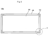
- FIG. 5 is a plan view illustrating a top substrate of a liquid crystal cell with an alignment mark according to an embodiment of the present invention
- FIGS. 6A and 6B are enlarged views of a portion B in FIG. 5 ;
- FIG. 7 is a plan view illustrating a bottom substrate of a liquid crystal cell with an alignment mark according to an embodiment of the present invention.
- FIG. 8 is an enlarged view of a portion C in FIG. 7 ;
- FIG. 9 is a plan view of an LCD according to another embodiment of the present invention.
- FIG. 3 is a plan view of a polarizing plate attached to an LCD with an alignment mark according to an embodiment of the present invention.
- an LCD includes a top substrate (a color filter substrate) 100 a having R, G and B color filters, a bottom substrate 100 b having pixel electrodes and TFTs, and a liquid crystal layer interposed between the top substrate 100 a and the bottom substrate 100 b . Also, a polarizing plate 150 is attached to a liquid crystal cell 100 formed by attaching the top substrate 100 a and the bottom substrate 100 b.
- An alignment mark 150 is formed in a corner region of the top substrate 100 a .
- the alignment mark 150 permits alignment of the polarizing plate 115 during attachment of the polarizing plate 115 to the liquid crystal cell 100 .
- the alignment mark can be formed in a black matrix region outside an active area of the top substrate 100 a , or can be formed in a corner region in an active area of the bottom substrate 100 b . That is, the alignment mark 150 can be formed on the top substrate 100 a or the bottom substrate 100 b of the liquid crystal cell 100 .
- the alignment mark 150 is formed in a ‘ ’-shape to align with a corner of the polarizing plate 115 .
- FIG. 4 is an enlarged view of a portion A in FIG. 3 .
- the alignment mark 150 has a calibrated gauge with a predetermined interval on an x-axis and a y-axis, and is divided with a predetermined angle ( ⁇ ) inside the x-axis and the y-axis.
- Misalignment includes tilting that can frequently occur during attachment of the polarizing plate 115 to the top substrate 100 a or the bottom substrate 100 b of the liquid crystal cell 100 . This misalignment can be prevented by aligning a corner of the polarizing plate 115 with the calibrated gauge of the x-axis and the y-axis or the angle ⁇ .
- FIG. 5 is a plan view illustrating the top substrate of the liquid crystal cell with the alignment mark according to an embodiment of the present invention.
- the alignment mark 150 is formed on the corner of an active area 105 in the top substrate 100 a so as enable precise attachment of the polarizing plate 115 thereto.
- the alignment mark 150 is formed by patterning a black matrix 106 of the top substrate 100 a.
- alignment marks 150 are illustrated in the corners of the active area 105 , more alignment marks 150 can also be formed along the corners of the active area 105 . Since the alignment mark 150 is formed together with the black matrix during manufacturing of the LCD, additional processes may be avoided in formation of the alignment mark 150 .
- FIGS. 6A and 6B are enlarged views of a portion B in FIG. 5 .
- the alignment mark 150 is formed together when the black matrix 106 is formed on the top substrate 100 a .
- the black matrix 106 is formed by photolithography.
- the black matrix 106 is formed in a lattice shape in an active area 105 of the top substrate 100 a , and is formed thickly enough to have a predetermined width for preventing light leakage around the corners.
- the alignment mark 150 is formed in an engraved shape with glass exposed by etching and patterning the black matrix 106 . That is, the alignment mark 150 is patterned when the black matrix 106 is patterned according to a photo process. Referring to FIG. 6A , the alignment mark 150 is formed to expose the transparent glass forming the top substrate 100 a by etching the black matrix 106 . Accordingly, the alignment mark 150 and the angle ⁇ are formed in a glass region that is exposed by an etching process.
- the alignment mark 150 can be formed of a material of the black matrix 106 in an embossed shape.
- the calibrated gauge and the angle ⁇ on the x-axis and the y-axis are formed of the material as the black matrix 106 .
- a color filter layer is formed in the active area 105 by using R, CG and B color resins. Misattachment of the polarizing plate can be prevented by forming the alignment mark 150 on the top substrate 100 a with the color filter layer so as to align the polarizing plate 115 .
- the polarizing plate 115 is then attached to the liquid crystal cell 100 .
- FIG. 7 is a plan view illustrating the bottom substrate of the liquid crystal cell with the alignment mark according to an embodiment of the present invention.
- FIG. 8 is an enlarged view of a portion C in FIG. 7 .
- the alignment mark 150 prevents misalignment when attaching the polarizing plate 115 on the bottom substrate 100 b , which has the TFTs and the pixel electrodes.
- the alignment mark 150 is formed on the corner region of the active area 109 with the TFTs and the pixel electrodes inside a pad region. That is, the alignment mark 150 is formed on the bottom substrate 100 b corresponding to the region in which the alignment mark is formed in FIG. 5 .
- the alignment mark 150 is formed on the bottom substrate 100 b when a gate line or data line is formed in manufacturing the bottom substrate 100 b . That is, when a metal layer from which a gate line, a gate electrode, and/or a gate pad are formed on the glass substrate, the alignment mark 150 is formed by patterning a metal layer in the corner region of the active area 109 . The alignment mark 150 is formed in a ‘ ’-shape.
- a thin film transistor, a data line, and a data pad are formed by forming an active layer and source/drain electrodes. Additionally, the active layer includes a gate insulating layer, a channel layer, and an ohmic contact layer.
- the alignment mark 150 can be formed during formation of the source/drain electrode, the data line, and/or the data pad. In this case, the alignment mark 150 is not formed during formation of the gate line but is formed by patterning a metal layer during formation of the data line.
- the alignment mark 150 is formed of a source/drain electrode metal, and is a ‘ ’-shaped structure in a corner of an active area 109 . Additionally, the alignment mark 150 is formed in each corner of the active area 109 . However, a plurality of alignment marks can be formed along with the perimeter of the active area 109 .
- the bottom substrate (the TFT substrate) 100 b is completed by forming a passivation layer and a pixel electrode. Accordingly, the alignment mark 150 can prevent misalignment and tilting of the polarizing plate 115 during the attachment process because the angle ⁇ and the calibrated gauge on the x-axis and the y-axis are formed to align the polarizing plate 115 .
- FIG. 9 is a plan view of an LCD according to another embodiment of the present invention.
- an alignment mark 250 prevents misalignment when attaching a polarizing plate 115 to a liquid crystal panel.
- a top substrate 200 a includes a color filter layer and a black matrix
- a bottom substrate 200 b includes TFTs and pixel electrodes.
- the liquid crystal panel 200 is formed by attaching the top substrate 200 a to the bottom substrate 200 b.
- the polarizing plate can be arranged by aligning a corner of the polarizing plate 115 with the alignment mark 250 .
- the alignment mark 250 of FIG. 9 has a broader range of use for aligning the polarizing plate 115 than that of FIG. 3 . Attachment still can be performed even if an end of the corner in the polarizing plate 115 is not disposed on the center of the cross as long as the corner of the polarizing plate 115 is overlapped with the alignment mark 250 , and is vertically and horizontally aligned with the alignment mark 250 .
- formation of the alignment mark 250 in the cross shape is identical to formation of the top substrate 100 a with the color filter and the black matrix, and the bottom substrate 100 b with the TFTs and pixel electrodes. Accordingly, a description about the formation of the alignment mark 250 in the cross shape will be omitted.
- the alignment mark of the polarizing plate can be used during attachment of the polarizing plate, and during attachment of other plates such as an optical sheet and a light guide plate in manufacturing the LCD. Accordingly, misalignment that frequently occurs during attachment of the polarizing plate, such as relative tilting between the polarizing plate and the substrate, can be prevented by forming an alignment mark to permit precise alignment of the polarizing plate with the LCD and accurately attach the polarizing plate to the liquid crystal cell.
Landscapes
- Physics & Mathematics (AREA)
- Nonlinear Science (AREA)
- Mathematical Physics (AREA)
- Chemical & Material Sciences (AREA)
- Crystallography & Structural Chemistry (AREA)
- General Physics & Mathematics (AREA)
- Optics & Photonics (AREA)
- Liquid Crystal (AREA)
- Optical Filters (AREA)
- Polarising Elements (AREA)
Priority Applications (1)
| Application Number | Priority Date | Filing Date | Title |
|---|---|---|---|
| US12/648,950 US8436966B2 (en) | 2005-06-27 | 2009-12-29 | Liquid crystal display device and manufacturing method thereof |
Applications Claiming Priority (3)
| Application Number | Priority Date | Filing Date | Title |
|---|---|---|---|
| KR10-2005-0055519 | 2005-06-27 | ||
| KR055519/2005 | 2005-06-27 | ||
| KR1020050055519A KR101183374B1 (ko) | 2005-06-27 | 2005-06-27 | 액정표시장치 및 그 제조방법 |
Related Child Applications (1)
| Application Number | Title | Priority Date | Filing Date |
|---|---|---|---|
| US12/648,950 Division US8436966B2 (en) | 2005-06-27 | 2009-12-29 | Liquid crystal display device and manufacturing method thereof |
Publications (2)
| Publication Number | Publication Date |
|---|---|
| US20060290874A1 US20060290874A1 (en) | 2006-12-28 |
| US7719637B2 true US7719637B2 (en) | 2010-05-18 |
Family
ID=37566883
Family Applications (2)
| Application Number | Title | Priority Date | Filing Date |
|---|---|---|---|
| US11/289,034 Active 2027-09-19 US7719637B2 (en) | 2005-06-27 | 2005-11-29 | Liquid crystal display device and manufacturing method thereof |
| US12/648,950 Active 2027-11-06 US8436966B2 (en) | 2005-06-27 | 2009-12-29 | Liquid crystal display device and manufacturing method thereof |
Family Applications After (1)
| Application Number | Title | Priority Date | Filing Date |
|---|---|---|---|
| US12/648,950 Active 2027-11-06 US8436966B2 (en) | 2005-06-27 | 2009-12-29 | Liquid crystal display device and manufacturing method thereof |
Country Status (4)
| Country | Link |
|---|---|
| US (2) | US7719637B2 (ko) |
| JP (1) | JP4344725B2 (ko) |
| KR (1) | KR101183374B1 (ko) |
| CN (1) | CN100514143C (ko) |
Cited By (4)
| Publication number | Priority date | Publication date | Assignee | Title |
|---|---|---|---|---|
| US20100006029A1 (en) * | 2003-12-10 | 2010-01-14 | Sung-Su Jung | Apparatus for aligning dispenser system, and dispenser alignment system |
| US20110109846A1 (en) * | 2009-11-09 | 2011-05-12 | Chunghwa Picture Tubes, Ltd. | Liquid crystal display with inspection structures for polarizer alignment |
| US20110181808A1 (en) * | 2010-01-27 | 2011-07-28 | Sony Corporation | Liquid crystal display device and electronic apparatus |
| US9082774B1 (en) * | 2014-07-21 | 2015-07-14 | Lg Display Co., Ltd. | Display device |
Families Citing this family (29)
| Publication number | Priority date | Publication date | Assignee | Title |
|---|---|---|---|---|
| JP4281584B2 (ja) * | 2004-03-04 | 2009-06-17 | セイコーエプソン株式会社 | 半導体装置の製造方法 |
| KR20070117110A (ko) * | 2006-06-07 | 2007-12-12 | 엘지.필립스 엘시디 주식회사 | 테이프 캐리어 패키지 및 이를 포함하는 액정표시장치 |
| TW200905262A (en) * | 2007-07-30 | 2009-02-01 | Chunghwa Picture Tubes Ltd | Color filter substrate and manufacturing thereof and liquid crystal display panel |
| KR100939214B1 (ko) * | 2008-06-12 | 2010-01-28 | 엘지디스플레이 주식회사 | 입체영상 표시장치의 정렬 시스템 및 방법 |
| KR20100022707A (ko) * | 2008-08-20 | 2010-03-03 | 삼성전자주식회사 | 액정 표시 장치 및 그 제조 방법 |
| CN101592816B (zh) * | 2009-04-10 | 2011-08-03 | 友达光电(苏州)有限公司 | 显示面板 |
| US8416370B2 (en) * | 2009-04-22 | 2013-04-09 | Japan Display Central Inc. | Liquid crystal display device having patterned alignment fiducial mark and method for manufacturing the same |
| JP5302345B2 (ja) * | 2011-02-09 | 2013-10-02 | 株式会社ジャパンディスプレイ | 表示装置 |
| KR101835557B1 (ko) * | 2011-10-07 | 2018-03-08 | 엘지디스플레이 주식회사 | 디스플레이 장치용 기판 및 그 제조방법 |
| TWI476459B (zh) * | 2012-05-03 | 2015-03-11 | Innocom Tech Shenzhen Co Ltd | 彩色濾光片基板,及觸控顯示裝置 |
| CN102707486B (zh) * | 2012-05-31 | 2015-07-15 | 深圳市华星光电技术有限公司 | 彩色滤光片基板及其制造方法 |
| CN103199084B (zh) * | 2013-03-08 | 2015-10-14 | 京东方科技集团股份有限公司 | 基板对位标记、基板及基板对位标记的制作方法 |
| KR20140127112A (ko) * | 2013-04-24 | 2014-11-03 | 삼성디스플레이 주식회사 | 액정 표시 장치 모니터링 장치 및 액정 표시 장치의 제조 방법 |
| JP5615962B2 (ja) * | 2013-06-20 | 2014-10-29 | 株式会社ジャパンディスプレイ | 表示装置 |
| WO2015008666A1 (ja) | 2013-07-19 | 2015-01-22 | 堺ディスプレイプロダクト株式会社 | 表示パネル及び表示装置 |
| KR102182881B1 (ko) * | 2013-11-13 | 2020-11-26 | 엘지디스플레이 주식회사 | 얼라인 키를 포함하는 표시패널 및 그 제조방법 |
| KR102143373B1 (ko) * | 2013-12-11 | 2020-08-12 | 엘지디스플레이 주식회사 | 스위처블 렌즈 장치와 그를 이용한 2d/3d 영상 표시장치 |
| CN104155795B (zh) * | 2014-08-26 | 2017-03-08 | 深圳市华星光电技术有限公司 | Cf基板的对组标记的制作方法 |
| JP6457875B2 (ja) | 2015-04-16 | 2019-01-23 | 株式会社ジャパンディスプレイ | 表示装置 |
| KR102509266B1 (ko) * | 2015-12-15 | 2023-03-10 | 엘지디스플레이 주식회사 | 액정 표시 장치 |
| JP6475773B2 (ja) * | 2016-06-06 | 2019-02-27 | 住友化学株式会社 | 積層フィルム、マーク付き積層フィルムの製造方法、及び、画像表示装置の製造方法 |
| CN106094311B (zh) * | 2016-08-22 | 2019-09-06 | 武汉华星光电技术有限公司 | 一种窄边框液晶面板及其组立标尺的制作方法 |
| CN107589570A (zh) * | 2017-09-25 | 2018-01-16 | 京东方科技集团股份有限公司 | 一种膜片及其对位方法、显示模组 |
| CN107632444B (zh) * | 2017-11-02 | 2020-10-16 | 上海天马微电子有限公司 | 异形显示面板及其制造方法及显示装置 |
| WO2020103272A1 (zh) * | 2018-11-21 | 2020-05-28 | 惠科股份有限公司 | 显示面板和显示装置 |
| CN110018590B (zh) * | 2019-04-22 | 2020-12-04 | 深圳市华星光电技术有限公司 | 液晶显示装置的制作方法 |
| TWI710821B (zh) * | 2019-06-04 | 2020-11-21 | 緯創資通股份有限公司 | 具有對位校準圖樣的面板裝置 |
| EP4148798A4 (en) | 2020-05-09 | 2023-06-07 | BOE Technology Group Co., Ltd. | DISPLAY PANEL AND METHOD OF MANUFACTURING THEREOF, AND DISPLAY DEVICE |
| RS64598B1 (sr) | 2021-05-25 | 2023-10-31 | Finance Force Glass 33 Doo | Slojeviti varijabilno transparentni panel |
Citations (15)
| Publication number | Priority date | Publication date | Assignee | Title |
|---|---|---|---|---|
| US4297004A (en) * | 1978-09-20 | 1981-10-27 | Technical Research of Citizen Watch Co., Ltd. | Liquid crystal display cell |
| US4721365A (en) * | 1984-11-21 | 1988-01-26 | Canon Kabushiki Kaisha | Electronic device including panels with electrical alignment means |
| JPS63113421A (ja) | 1986-10-30 | 1988-05-18 | Toshiba Corp | 液晶表示器の製造方法 |
| US5058997A (en) * | 1989-08-11 | 1991-10-22 | International Business Machines Corporation | Tft lcd with optical interference color filters |
| JPH05107518A (ja) | 1991-10-18 | 1993-04-30 | Sony Corp | 液晶表示装置およびその製造方法 |
| US5285302A (en) * | 1992-03-30 | 1994-02-08 | Industrial Technology Research Institute | TFT matrix liquid crystal display with compensation capacitance plus TFT stray capacitance constant irrespective of mask misalignment during patterning |
| US5708483A (en) * | 1993-07-13 | 1998-01-13 | Kabushiki Kaisha Toshiba | Active matrix type display device |
| US5731860A (en) * | 1995-06-28 | 1998-03-24 | Sharp Kabushiki Kaisha | Method of manufacturing liquid crystal panel and press device to be adopted in the method |
| US5739887A (en) * | 1994-10-21 | 1998-04-14 | Hitachi, Ltd. | Liquid crystal display device with reduced frame portion surrounding display area |
| US5771085A (en) * | 1995-11-06 | 1998-06-23 | Sony Corporation | LCD device with an alignment mark having same material as microlenses |
| JPH10282464A (ja) | 1997-04-11 | 1998-10-23 | Nec Corp | 液晶表示装置及びその製造方法 |
| JP2000066179A (ja) | 1998-08-24 | 2000-03-03 | Nec Corp | 液晶表示素子とその製造方法 |
| JP2000147485A (ja) | 1998-11-05 | 2000-05-26 | Nec Corp | 液晶表示パネル |
| JP2000221462A (ja) | 1999-01-29 | 2000-08-11 | Seiko Epson Corp | 電気光学装置の製造方法 |
| JP2002174803A (ja) | 2000-12-07 | 2002-06-21 | Seiko Epson Corp | 電気光学装置および電子機器 |
Family Cites Families (1)
| Publication number | Priority date | Publication date | Assignee | Title |
|---|---|---|---|---|
| KR100855884B1 (ko) * | 2001-12-24 | 2008-09-03 | 엘지디스플레이 주식회사 | 액정표시장치용 얼라인 키 |
-
2005
- 2005-06-27 KR KR1020050055519A patent/KR101183374B1/ko active IP Right Grant
- 2005-11-29 US US11/289,034 patent/US7719637B2/en active Active
- 2005-12-08 CN CNB2005101304433A patent/CN100514143C/zh active Active
- 2005-12-09 JP JP2005356399A patent/JP4344725B2/ja active Active
-
2009
- 2009-12-29 US US12/648,950 patent/US8436966B2/en active Active
Patent Citations (16)
| Publication number | Priority date | Publication date | Assignee | Title |
|---|---|---|---|---|
| US4297004A (en) * | 1978-09-20 | 1981-10-27 | Technical Research of Citizen Watch Co., Ltd. | Liquid crystal display cell |
| US4721365A (en) * | 1984-11-21 | 1988-01-26 | Canon Kabushiki Kaisha | Electronic device including panels with electrical alignment means |
| JPS63113421A (ja) | 1986-10-30 | 1988-05-18 | Toshiba Corp | 液晶表示器の製造方法 |
| US5058997A (en) * | 1989-08-11 | 1991-10-22 | International Business Machines Corporation | Tft lcd with optical interference color filters |
| JPH05107518A (ja) | 1991-10-18 | 1993-04-30 | Sony Corp | 液晶表示装置およびその製造方法 |
| US5285302A (en) * | 1992-03-30 | 1994-02-08 | Industrial Technology Research Institute | TFT matrix liquid crystal display with compensation capacitance plus TFT stray capacitance constant irrespective of mask misalignment during patterning |
| US5708483A (en) * | 1993-07-13 | 1998-01-13 | Kabushiki Kaisha Toshiba | Active matrix type display device |
| US5739887A (en) * | 1994-10-21 | 1998-04-14 | Hitachi, Ltd. | Liquid crystal display device with reduced frame portion surrounding display area |
| US5731860A (en) * | 1995-06-28 | 1998-03-24 | Sharp Kabushiki Kaisha | Method of manufacturing liquid crystal panel and press device to be adopted in the method |
| US5771085A (en) * | 1995-11-06 | 1998-06-23 | Sony Corporation | LCD device with an alignment mark having same material as microlenses |
| JPH10282464A (ja) | 1997-04-11 | 1998-10-23 | Nec Corp | 液晶表示装置及びその製造方法 |
| JP2000066179A (ja) | 1998-08-24 | 2000-03-03 | Nec Corp | 液晶表示素子とその製造方法 |
| JP2000147485A (ja) | 1998-11-05 | 2000-05-26 | Nec Corp | 液晶表示パネル |
| US6307613B1 (en) | 1998-11-05 | 2001-10-23 | Nec Corporation | Liquid crystal display panel with plurality of alignment marks within the wiring layer |
| JP2000221462A (ja) | 1999-01-29 | 2000-08-11 | Seiko Epson Corp | 電気光学装置の製造方法 |
| JP2002174803A (ja) | 2000-12-07 | 2002-06-21 | Seiko Epson Corp | 電気光学装置および電子機器 |
Non-Patent Citations (2)
| Title |
|---|
| First Office Action for corresponding Chinese Patent Application Serial No. 2005101304433, dated Dec. 14, 2007. |
| Office Action dated Feb. 10, 2009 for Japanese Patent No. 2005-356399. |
Cited By (6)
| Publication number | Priority date | Publication date | Assignee | Title |
|---|---|---|---|---|
| US20100006029A1 (en) * | 2003-12-10 | 2010-01-14 | Sung-Su Jung | Apparatus for aligning dispenser system, and dispenser alignment system |
| US9004005B2 (en) * | 2003-12-10 | 2015-04-14 | Lg Display Co., Ltd. | Apparatus for aligning dispenser using alignment plate and dispenser alignment system |
| US20110109846A1 (en) * | 2009-11-09 | 2011-05-12 | Chunghwa Picture Tubes, Ltd. | Liquid crystal display with inspection structures for polarizer alignment |
| US20110181808A1 (en) * | 2010-01-27 | 2011-07-28 | Sony Corporation | Liquid crystal display device and electronic apparatus |
| US8395749B2 (en) * | 2010-01-27 | 2013-03-12 | Sony Corporation | Liquid crystal display device and electronic apparatus |
| US9082774B1 (en) * | 2014-07-21 | 2015-07-14 | Lg Display Co., Ltd. | Display device |
Also Published As
| Publication number | Publication date |
|---|---|
| KR101183374B1 (ko) | 2012-09-21 |
| CN1888958A (zh) | 2007-01-03 |
| KR20070000075A (ko) | 2007-01-02 |
| US20100134725A1 (en) | 2010-06-03 |
| US8436966B2 (en) | 2013-05-07 |
| JP2007004111A (ja) | 2007-01-11 |
| US20060290874A1 (en) | 2006-12-28 |
| CN100514143C (zh) | 2009-07-15 |
| JP4344725B2 (ja) | 2009-10-14 |
Similar Documents
| Publication | Publication Date | Title |
|---|---|---|
| US7719637B2 (en) | Liquid crystal display device and manufacturing method thereof | |
| US8045127B2 (en) | Fabricating methods of a liquid crystal display comprising first and second align marks | |
| US7460204B2 (en) | Liquid crystal display device and manufacturing method thereof | |
| US8049222B2 (en) | Display device and method of manufacturing the same | |
| US8400606B2 (en) | Liquid crystal display apparatus and method of manufacturing the same | |
| US7050131B2 (en) | Liquid crystal display device having black seal pattern and external resin pattern, and method of fabricating the same | |
| US20200166795A1 (en) | Manufacturing method for flexible liquid crystal display panel | |
| GB2424509A (en) | Color filter array substrate and fabricating method thereof | |
| JP2010096856A (ja) | 液晶表示装置 | |
| US20080239188A1 (en) | Display substrate, liquid crystal display device having the same and method of manufacturing the same | |
| US20070052908A1 (en) | Liquid crystal display and method for manufacturing the same | |
| KR102067964B1 (ko) | 액정표시장치 및 이의 제조방법 | |
| US20070024799A1 (en) | Display device | |
| WO2018205358A1 (zh) | 一种显示面板和显示装置 | |
| US6829022B2 (en) | Chuck for exposure apparatus | |
| JP2002333628A (ja) | 液晶表示装置、カラーフィルタ基板およびアレイ基板 | |
| KR20070071985A (ko) | 액정표시장치용 컬러필터 기판 및 그의 제조 방법 | |
| KR101024642B1 (ko) | 액정표시패널 및 그 제조방법 | |
| JP2007017756A (ja) | 液晶表示装置 | |
| US20070178390A1 (en) | Exposure mask, liquid crystal display device using the same, and method of manufacturing liquid crystal display device using the same | |
| JP2004077703A (ja) | 液晶表示装置 | |
| KR100471766B1 (ko) | 반도체장치의제조장치 | |
| US20020191146A1 (en) | Method for fabricating a liquid crystal display device | |
| KR20060008002A (ko) | 액정표시패널 및 그 제조방법 | |
| KR20060136045A (ko) | 액정표시장치 및 그 제조방법 |
Legal Events
| Date | Code | Title | Description |
|---|---|---|---|
| AS | Assignment |
Owner name: LG. PHILIPS LCD CO., LTD.,KOREA, REPUBLIC OF Free format text: ASSIGNMENT OF ASSIGNORS INTEREST;ASSIGNORS:PAIK, SANG YOON;LEE, JOON YOUP;REEL/FRAME:017302/0492 Effective date: 20051129 Owner name: LG. PHILIPS LCD CO., LTD., KOREA, REPUBLIC OF Free format text: ASSIGNMENT OF ASSIGNORS INTEREST;ASSIGNORS:PAIK, SANG YOON;LEE, JOON YOUP;REEL/FRAME:017302/0492 Effective date: 20051129 |
|
| AS | Assignment |
Owner name: LG DISPLAY CO., LTD.,KOREA, REPUBLIC OF Free format text: CHANGE OF NAME;ASSIGNOR:LG PHILIPS LCD CO., LTD.;REEL/FRAME:020986/0231 Effective date: 20080229 Owner name: LG DISPLAY CO., LTD., KOREA, REPUBLIC OF Free format text: CHANGE OF NAME;ASSIGNOR:LG PHILIPS LCD CO., LTD.;REEL/FRAME:020986/0231 Effective date: 20080229 |
|
| FEPP | Fee payment procedure |
Free format text: PAYOR NUMBER ASSIGNED (ORIGINAL EVENT CODE: ASPN); ENTITY STATUS OF PATENT OWNER: LARGE ENTITY |
|
| STCF | Information on status: patent grant |
Free format text: PATENTED CASE |
|
| FPAY | Fee payment |
Year of fee payment: 4 |
|
| MAFP | Maintenance fee payment |
Free format text: PAYMENT OF MAINTENANCE FEE, 8TH YEAR, LARGE ENTITY (ORIGINAL EVENT CODE: M1552) Year of fee payment: 8 |
|
| MAFP | Maintenance fee payment |
Free format text: PAYMENT OF MAINTENANCE FEE, 12TH YEAR, LARGE ENTITY (ORIGINAL EVENT CODE: M1553); ENTITY STATUS OF PATENT OWNER: LARGE ENTITY Year of fee payment: 12 |