US7627697B2 - Device using multiple DMA controllers for transferring data between a storage device and multiple processing units - Google Patents
Device using multiple DMA controllers for transferring data between a storage device and multiple processing units Download PDFInfo
- Publication number
- US7627697B2 US7627697B2 US10/896,887 US89688704A US7627697B2 US 7627697 B2 US7627697 B2 US 7627697B2 US 89688704 A US89688704 A US 89688704A US 7627697 B2 US7627697 B2 US 7627697B2
- Authority
- US
- United States
- Prior art keywords
- dma
- arithmetic units
- arithmetic
- control circuit
- processor
- Prior art date
- Legal status (The legal status is an assumption and is not a legal conclusion. Google has not performed a legal analysis and makes no representation as to the accuracy of the status listed.)
- Expired - Fee Related, expires
Links
- 238000012545 processing Methods 0.000 title claims abstract description 78
- 238000003860 storage Methods 0.000 title claims abstract description 31
- 238000012546 transfer Methods 0.000 claims abstract description 75
- 230000014759 maintenance of location Effects 0.000 claims description 4
- 238000000034 method Methods 0.000 description 59
- 238000010586 diagram Methods 0.000 description 30
- 238000012544 monitoring process Methods 0.000 description 4
- 238000003672 processing method Methods 0.000 description 4
- 230000006870 function Effects 0.000 description 3
- 238000004891 communication Methods 0.000 description 2
- 230000002093 peripheral effect Effects 0.000 description 1
- 230000004044 response Effects 0.000 description 1
Images


Classifications
-
- F—MECHANICAL ENGINEERING; LIGHTING; HEATING; WEAPONS; BLASTING
- F16—ENGINEERING ELEMENTS AND UNITS; GENERAL MEASURES FOR PRODUCING AND MAINTAINING EFFECTIVE FUNCTIONING OF MACHINES OR INSTALLATIONS; THERMAL INSULATION IN GENERAL
- F16K—VALVES; TAPS; COCKS; ACTUATING-FLOATS; DEVICES FOR VENTING OR AERATING
- F16K3/00—Gate valves or sliding valves, i.e. cut-off apparatus with closing members having a sliding movement along the seat for opening and closing
- F16K3/30—Details
- F16K3/314—Forms or constructions of slides; Attachment of the slide to the spindle
-
- G—PHYSICS
- G06—COMPUTING; CALCULATING OR COUNTING
- G06F—ELECTRIC DIGITAL DATA PROCESSING
- G06F9/00—Arrangements for program control, e.g. control units
- G06F9/06—Arrangements for program control, e.g. control units using stored programs, i.e. using an internal store of processing equipment to receive or retain programs
- G06F9/30—Arrangements for executing machine instructions, e.g. instruction decode
- G06F9/38—Concurrent instruction execution, e.g. pipeline or look ahead
- G06F9/3877—Concurrent instruction execution, e.g. pipeline or look ahead using a slave processor, e.g. coprocessor
-
- F—MECHANICAL ENGINEERING; LIGHTING; HEATING; WEAPONS; BLASTING
- F16—ENGINEERING ELEMENTS AND UNITS; GENERAL MEASURES FOR PRODUCING AND MAINTAINING EFFECTIVE FUNCTIONING OF MACHINES OR INSTALLATIONS; THERMAL INSULATION IN GENERAL
- F16K—VALVES; TAPS; COCKS; ACTUATING-FLOATS; DEVICES FOR VENTING OR AERATING
- F16K31/00—Actuating devices; Operating means; Releasing devices
- F16K31/44—Mechanical actuating means
- F16K31/53—Mechanical actuating means with toothed gearing
-
- F—MECHANICAL ENGINEERING; LIGHTING; HEATING; WEAPONS; BLASTING
- F16—ENGINEERING ELEMENTS AND UNITS; GENERAL MEASURES FOR PRODUCING AND MAINTAINING EFFECTIVE FUNCTIONING OF MACHINES OR INSTALLATIONS; THERMAL INSULATION IN GENERAL
- F16K—VALVES; TAPS; COCKS; ACTUATING-FLOATS; DEVICES FOR VENTING OR AERATING
- F16K31/00—Actuating devices; Operating means; Releasing devices
- F16K31/44—Mechanical actuating means
- F16K31/60—Handles
-
- G—PHYSICS
- G06—COMPUTING; CALCULATING OR COUNTING
- G06F—ELECTRIC DIGITAL DATA PROCESSING
- G06F13/00—Interconnection of, or transfer of information or other signals between, memories, input/output devices or central processing units
- G06F13/14—Handling requests for interconnection or transfer
- G06F13/20—Handling requests for interconnection or transfer for access to input/output bus
- G06F13/28—Handling requests for interconnection or transfer for access to input/output bus using burst mode transfer, e.g. direct memory access DMA, cycle steal
Definitions
- the present invention relates to a processor system which can perform a data transfer process by DMA (Direct Memory Access), a DMA control circuit, a DMA control method, a control method for DMA controller, a graphic processing method, and a graphic processing circuit.
- DMA Direct Memory Access
- DMA transfer data transfer is performed in parallel with an operation of a host processor to reduce processing load on the host processor. While the DMA transfer is performed, the host processor can perform another process. For this reason, the DMA transfer is suitably applied to a case in which a large amount of data such as image data is transferred.
- a DMA transfer is generally performed under the control of a DMA controller.
- a host processor sets transfer control information representing time when a DMA transfer is performed, a position from which the DMA transfer is performed, and a position to which the DMA transfer is performed in the DMA controller in advance. According to the setting information, the DMA controller performs the DMA transfer.
- the host processor when the plurality of DMA controllers are arranged to make it possible to perform data transfer processes in parallel to each other, the host processor must set pieces of transfer control information for the DMA controllers, processing load on the host processor increases. The processing load increases in proportion to the number of DMA controllers.
- a processor system preferably includes
- a storage configured to store data that the arithmetic units use for arithmetic processing.
- the processor system preferably includes a plurality of DMA controllers which perform data transfer between the arithmetic units, and between the arithmetic units and the storage in parallel with processings of a host processor.
- the system may also include
- DMA control circuit which controls start-up of the arithmetic units and the DMA controllers in parallel with processings of the host processor.
- a DMA control circuit preferably includes
- a scheduler which performs data transfer between a plurality of arithmetic units each being capable of performing arithmetic processings in parallel, data transfer between a storage which stores data that the arithmetic units use for arithmetic processings and the arithmetic units, and starting control of the arithmetic units, based information stored in the instruction storages, in parallel with processings of the host processor.
- a method of controlling a DMA controller is provided.
- the method preferably includes the steps of
- the method preferably also includes the step of
- the method preferably also includes the step of
- a graphic processing method is provided.
- the graphic processing method preferably includes the steps of
- the method preferably further includes the steps of
- the method can also include the step of
- a graphic processing circuit is provided.
- the processing circuit preferably includes
- a pixel information converter which converts vertex information into pixel information
- the processing circuit further includes
- control circuit which determines whether DMA transfer by the DMA controllers is possible, based on instruction information stored in the instruction information storage.
- FIG. 1 is a block diagram showing a schematic configuration of a processor system according to the first embodiment of the present invention.
- FIG. 2 is a block diagram showing the details of the internal configuration of the graphic processing processor 2 shown in FIG. 1 .
- FIG. 3 is a block diagram showing an example of the internal configuration of the controller 21 .
- FIG. 4 is a block diagram showing an example of the internal configuration of the dedicated circuit 32 in FIG. 3 .
- FIG. 5 is a flow chart showing an example of procedures performed by the controller 21 in FIG. 1 .
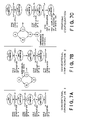
- FIGS. 6A and 6B are diagrams showing an example of tasks executed by the dedicated circuit 32 .
- FIG. 7A is a diagram showing a first operation of a conventional DMAC 31
- FIG. 7B is a diagram showing a second operation of the conventional DMAC 31
- FIG. 7C is a diagram showing an operation of the DMAC 31 according to this embodiment.
- FIG. 8 is a timing chart corresponding to FIG. 7A .
- FIG. 9 is a timing chart corresponding to FIG. 7B .
- FIG. 10 is a timing chart corresponding to FIG. 7C .
- FIG. 11 is a diagram showing one example of how to use the sync register.
- FIG. 12 is a diagram showing another example of how to use the sync register.
- FIG. 13 is a diagram showing another example of how to use the sync register.
- FIG. 14 is a diagram showing a method of processing two instruction strings.
- FIG. 15 is a data flow chart showing an example of procedures of the controller 21 .
- FIG. 16 is a diagram showing one example of a program of the host processor 1 .
- FIG. 17 is a block diagram showing the internal configuration of the controller 21 according to the second embodiment.
- FIG. 18 is a block diagram showing an example of the internal configuration of the dedicated circuit 32 a in FIG. 17 .
- FIG. 19 is a flow chart showing an example of a procedure performed by the controller 21 in FIG. 17 .
- FIG. 20 is a block diagram showing a case in which the processor system according to this application is built in a digital television set.
- FIG. 21 is a block diagram showing an example in which the processor system according to this embodiment is built in a video recorder/player.
- a processor system, a DMA control circuit, a DMA control method, a control method for a DMA controller, a graphic processing method, and a graphic processing circuit will be described below with reference to the accompanying drawings.
- FIG. 1 is a block diagram showing a schematic configuration of a processor system according to the first embodiment of the present invention.
- the processor system shown in FIG. 1 includes a host processor 1 , a graphic processing processor 2 , a main memory 3 , and an I/O processor 4 .
- the host processor 1 includes a main processor 11 , a plurality of digital signal processors (DSP) 12 , and I/O units 13 , 14 , and 15 which controls input/output operations with an external circuit.
- the I/O unit 13 controls input/output operations with the main memory 3
- the I/O unit 14 controls the input/output operations with the graphic processing processor 2
- the I/O unit 15 controls the input/output operations with the I/O processor 4 .
- the graphic processing processor 2 includes a controller 21 serving as a characteristic part of this embodiment, an I/O unit 22 which performs data exchange with the host processor 1 , various universal buses such as a PCI bus, an I/O unit 23 which controls input/output operations of video data, audio data, or the like, and a graphic processing unit 24 which performs graphic processing calculation.
- a controller 21 serving as a characteristic part of this embodiment
- an I/O unit 22 which performs data exchange with the host processor 1
- various universal buses such as a PCI bus
- an I/O unit 23 which controls input/output operations of video data, audio data, or the like
- a graphic processing unit 24 which performs graphic processing calculation.
- the graphic processing unit 24 includes a pixel converters 26 which converts the vertex information of a polygon into pixel data and a plurality of arithmetic units (DSP) 27 which process the pixel data.
- DSP arithmetic units
- the I/O processor 4 controls connection to a universal bus, a peripheral devices such as an HDD and a DVD or the like, and a network.
- FIG. 2 is a block diagram showing the details of the internal configuration of the graphic processing processor 2 shown in FIG. 1 .
- Each of the plurality of arithmetic units 27 includes a processor cluster 28 constituted by a plurality of processors and a memory 29 which stores a processing results of the processor cluster 28 .
- the plurality of processors in the processor cluster 28 can execute independent processes in parallel to each other, and can execute one process such that the plurality of processor cluster 28 share the process.
- the memory 29 stores an execution result of the processor cluster 28 .
- the controller 21 , the pixel converters 26 , the I/O units 22 and 23 , and the memory 29 which are shown in FIG. 2 are connected to a common bus 30 .
- FIG. 3 is a block diagram showing an example of the internal configuration of the controller 21 .
- the controller 21 shown in FIG. 3 includes a plurality of DMA controllers (DMAC) 31 , a dedicated circuit 32 , a control processor 33 constituted by general-purpose processors, a timer 34 , an interruption unit 35 and a memory 36 .
- DMAC DMA controllers
- the DMA controllers 31 perform data transfer between the plurality of arithmetic units 27 and between the plurality of arithmetic units 27 and the memory 36 .
- the dedicated circuit 32 is a circuit which is dedicated to this system, and performs start-up control for the DMA controllers 31 and the arithmetic units 27 .
- the control processor 33 controls the dedicated circuit 32 according to a program code stored in the memory 36 or an instruction from the host processor 1 .
- the timer 34 performs time management and instructs the interruption unit 35 to perform interruption as needed.
- the interruption unit 35 receives a signal from the timer 34 or a completion signal from the DMA controllers 31 or the arithmetic units 27 to perform interruption to the control processor 33 .
- the dedicated circuit 32 , the timer 34 , the interruption unit 35 , and the memory 36 shown in FIG. 3 are connected to a local network 37 .
- the host processor 1 is also connected to the local network 37 through the I/O unit 22 .
- the memory 36 is, for example, consisted of an embedded DRAM.
- the DMA controllers are, for example, provided more than 30 pieces.
- FIG. 4 is a block diagram showing an example of the internal configuration of the dedicated circuit 32 in FIG. 3 .
- This block diagram shows a configuration in which the dedicated circuit 32 is connected as a co-processor of the control processor 33 .
- the dedicated circuit 32 in FIG. 4 includes a control processor I/O unit 41 , a plurality of DMA registers 42 , a DMA issuance unit 43 , a plurality of sync registers 44 , and a sync register control units 45 .
- the control processor I/O unit 41 exchanges data with the control processor 33 .
- the DMA registers 42 stores various pieces of information required for the operations of the DMACs 31 .
- the DMA issuance unit 43 performs a process of transferring the pieces of information in the DMA registers 42 to the DMACs 31 .
- a specific DMA register from which the information is transferred and a specific DMAC 31 to which the information is transferred are determined by the control processor 33 .
- the DMA issuance unit 43 is notified of the specific DMA register and the specific DMAC 31 through the control processor I/O unit 41 .
- the sync registers 44 stores the operation states of the DMACs 31 and the arithmetic units 27 .
- the sync register control units 45 controls updating of the sync registers 44 .
- FIG. 5 is a flow chart showing an example of procedures performed by the controller 21 in FIG. 1 . This flow chart shows procedures performed when data prepared in the host processor 1 is DMA-transferred to the memory 36 in the graphic processing processor 2 .
- the host processor 1 transmits a preparation completion signal to the local network 37 in FIG. 3 . This signal is received by the sync register control unit 45 in FIG. 4 (step S 1 ).
- the sync register control unit 45 updates the value of the sync register 44 (step S 2 ). More specifically, the sync register 44 is set at a value representing that preparation for data transfer of the host processor 1 is completed.
- the control processor 33 reads the value of the sync register 44 through the control processor I/O unit 41 according to a dedicated instruction to confirm that the preparation for the host processor 1 is completed (step S 3 ).
- the dedicated instruction expresses a task.
- An instruction string including the dedicated instruction (task) executed by the control processor 33 and the dedicated circuit 32 expresses a task string.
- the control processor 33 transfers the setting information of the DMAC 31 to the DMA register 42 through the control processor I/O unit 41 (step S 4 ).
- the control processor 33 starts the DMA issuance unit 43 through the control processor I/O unit 41 based on a dedicated instruction, and instructs the DMA issuance unit 43 to set the setting information of the DMAC 31 stored in the DMA registers 42 in each DMAC 31 (step S 5 ).
- the DMAC 31 performs a DMA transfer.
- the DMAC 31 notifies the sync register control units 45 that the DMA transfer is completed (step S 6 ).
- the sync register control units 45 updates the sync register 44 (step S 7 ).
- the control processor 33 reads the value of the sync resister through the control processor I/O unit 41 based on a dedicated instruction, and confirms that the DMA transfer is completed (step S 8 ). Thereafter, the control processor 33 starts the arithmetic unit 27 through the control processor I/O unit 41 , and processes data transferred from the host processor 1 to the memory in the graphic processing processor 2 (step S 9 ).
- the sync register control unit 45 in FIG. 4 monitors the value of the sync registers 44 . Periodical monitoring is generally called “polling”.
- the sync register control unit 45 according to this embodiment can monitor the operations of the DMAC 31 , the arithmetic unit 27 , and the host processor 1 by the polling.
- control processor 33 may monitor the sync register 44 through the control processor I/O unit 41 .
- a command for controlling the DMAC 31 is called an instruction, and each command is constituted of, e.g., 256-bit data.
- the sync register control unit 45 and the sync register 44 in the dedicated circuit 32 serve as a task scheduler.
- the task includes a command related to data transfer control of the DMAC 31 and a command related to start-up control of the arithmetic units 27 and an initial setting for the arithmetic units 27 , and a command related to an interruption notice for the host processor 1 .
- the dedicated circuit 32 continuously execute tasks until a special task called a block task is executed.
- the block task is a task which waits for execution completion of a task (DMA execution or a process of a processor cluster) issued before the block task.
- the dedicated circuit 32 waits until the execution of the set tasks is completed.
- FIG. 6A is a diagram showing an example of tasks executed by the dedicated circuit 32 , and shows an example in which tasks A, B, C, D, E, F, and G are executed.
- the tasks in FIG. 6A are written as a data flow chart as shown in FIG. 6B .
- the dedicated circuit 32 executes task A and waits for execution completion of task A as a block task.
- the dedicated circuit 32 executes tasks F and B in parallel.
- the dedicated circuit 32 waits execution completion of the tasks F and B as block tasks.
- the dedicated circuit 32 executes tasks C and D in parallel.
- the dedicated circuit 32 waits for execution completion of the tasks C and D as block tasks.
- the dedicated circuit 32 executes task E.
- the dedicated circuit 32 waits execution completion of task E as a block task.
- the dedicated circuit 32 executes task G.
- a block task in FIG. 6B can synchronize a plurality of DMA transfers.
- the dedicated circuit 32 of this embodiment can start the following DMA transfer by an event except for a notice of completion of a DMA transfer.
- the event mentioned here is, e.g., completion of a calculation process of the arithmetic units 27 or a notice from the host processor 1 .
- FIG. 7A is a diagram showing a first operation of a conventional DMAC 31
- FIG. 7B is a diagram showing a second operation of the conventional DMAC 31
- FIG. 7C is a diagram showing an operation of the DMAC 31 according to this embodiment.
- FIG. 8 is a timing chart corresponding to FIG. 7A
- FIG. 9 is a timing chart corresponding to FIG. 7B
- FIG. 10 is a timing chart corresponding to FIG. 7C .
- FIGS. 7A and 8 show most popular DMA transfers. After a certain DMA transfer is completed, the next DMA transfer is performed. In this case, as shown in FIG. 8 , the host processor 1 (CPU) performs designation (t 1 ) of DMA, register setting (t 2 ) of the arithmetic unit 27 , and designation of execution (t 3 ) of the arithmetic unit 27 . The DMAC 31 executes a DMA command designated by the host processor 1 .
- a plurality of DMA transfers can be performed in parallel to each other.
- the host processor 1 performs the register setting and the designation of start of the arithmetic unit 27 (period t 5 ).
- the DMAC 31 transfers the register setting and the designation of start of the arithmetic unit 27 (period t 6 ).
- the register setting can be performed to the plurality of DMACs 31 in parallel, when the number of registers to be resister-set is large, processing load on the host processor 1 can be reduced. However, when only some registers are reset, as in the cases in FIGS. 7A and 8 , the processing load on the host processor 1 increases.
- the next DMA transfer is performed by using only the end of a DMA transfer as a trigger, but also the next DMA transfer is performed by using a notice from the arithmetic unit 27 or the host processor 1 as a trigger.
- the DMAC 31 can perform register setting of the arithmetic unit 27 and designation of execution of the arithmetic unit 27 . More specifically, as shown in FIG.
- the DMAC 31 when the host processor 1 designates the DMAC 31 to perform a DMA transfer (period t 7 ), in response to this designation, the DMAC 31 performs register setting (period t 8 ) of the arithmetic unit 27 , a DMA transfer (period t 9 ), and designation of execution (period t 10 ) of the arithmetic unit 27 . Upon completion of the calculation process, the arithmetic unit 27 notifies the DMAC 31 of the end of the calculation process.
- the host processor 1 can allocate long time to other processes. Therefore, the performance of the host processor 1 can be enhanced.
- the host processor 1 reads a task string stored in the main memory 3 to transfer the task string to a memory in the graphic processing processor 2 .
- This transfer process may be directly written in the memory by a store task of the host processor 1 , or a DMA transfer may be performed as one of tasks.
- the sync register control units 45 in the controller 21 sets pointer information or the like of a task string in the DMA register 42 of the DMAC 31 . According to the contents of the DMA registers 42 , the DMA issue device performs various settings to each DMAC 31 .
- the controller 21 can perform not only start-up control of the DMAC 31 but also start-up control of the arithmetic unit 27 .
- tasks used when the controller 21 controls the arithmetic unit 27 tasks of two types, i.e., a set task and a kick task are known.
- the set task is a task for performing various settings to the arithmetic unit 27 . More specifically, various settings are performed to display a three-dimensional image such as a texture or a vertex.
- the kick task is a task for designating the start of execution of the arithmetic unit 27 .
- the operation states of the DMAC 31 , the arithmetic unit 27 , and the like are stored.
- the host processor 1 can read the value of the sync registers 44 through the sync register control units 45 .
- Several methods may be used as methods of using the sync register 44 . Typical one of these methods is shown in FIGS. 11 , 12 , and 13 .
- step S 11 some process is performed by the controller 21 (step S 11 ).
- the process result is written in the sync register 44 by a write task (step S 12 ).
- the controller 21 interrupts the execution of the task until the controller 21 receives a notice for block cancellation from the host processor 1 (step S 13 ).
- step S 14 the host processor 1 periodically performs polling of the sync register 44 (step S 14 ) to acquire the values written in the sync register 44 in the write task, the host processor 1 notifies the controller 21 of block cancellation (step S 15 ).
- the controller 21 starts the arithmetic unit 27 by a kick task (step S 16 ), and interrupts the execution of the tasks until the process in the arithmetic unit 27 is ended (step S 17 ).
- the arithmetic unit 27 started by the kick task executes some process (step S 18 ).
- the arithmetic unit 27 transmits a completion notice to the controller 21 and writes a return value in the sync register 44 (step S 19 ).
- the controller 21 which receives the completion notice performs branching with reference to a value of a general-purpose register (step S 20 ).
- step S 21 some process is performed by the controller 21 (step S 21 ).
- the execution of the task is interrupted until the controller 21 receives a notice of block cancellation from the host processor 1 (step S 22 ).
- the host processor 1 dynamically sets time when the execution of the task is restarted by the controller 21 (step S 23 ). At that time, the host processor 1 cancels the block of the controller 21 and writes the return value in the sync register 44 (step S 24 ).
- the controller 21 performs branching with reference to the value of the sync register 44 (step S 25 ).
- the controller 21 can simultaneously execute a plurality of task strings.
- a program which is executed such that data is transferred from the main memory 3 to a memory and the pointer of the data is set in the arithmetic unit 27 will be described below.
- the controller 21 simultaneously executes two task strings and synchronizes the task strings. This synchronization is performed by designation from the host processor 1 .
- the memory is divided into four regions (to be referred to as first-in-first-out (FIFO) 0 to 3 hereinafter).
- FIFO first-in-first-out
- the main memory 3 transfers data to FIFO 0 to 3 .
- the other task string (to be referred to as Task String 2 ), data is transferred from FIFO 0 to 3 to the arithmetic unit 27 .
- Task String 2 actually performs an initial setting to the arithmetic unit 27 by a set task.
- the arithmetic unit 27 reads the data from the memory.
- FIG. 15 is a data flow chart showing an example of procedures of the controller 21 which executes two Task Strings 1 and 2 described above.
- Task String 1 and Task String 2 in FIG. 15 are executed in parallel to each other.
- data is sequentially transferred from the main memory 3 to FIFO 0 to 3 .
- the controller 21 returns to the top of Task String 1 (step S 31 to S 39 ).
- the controller 21 receives a notice of block cancellation from the host processor 1 , the controller 21 performs the next data transfer process.
- Task String 2 the addresses of FIFO 0 to 3 are set in the arithmetic units 27 , processes for designating the arithmetic units 27 to start are sequentially repeated, and the controller 21 returns to the top of Task String 2 (step S 41 to S 54 ). After the addresses of FIFO 0 to 3 are set in the arithmetic units 27 , the process is interrupted. When the host processor 1 cancels the block, the next process is performed.
- FIG. 16 An example of a program of the host processor 1 for realizing the processes in FIG. 15 is as shown in FIG. 16 .
- the graphic processing processor 2 having the controller 21 for performing start-up control of the plurality of DMACs 31 and the plurality of arithmetic units 27 is arranged independently of the host processor 1 , so that control of the DMACs 31 and start designation of the arithmetic units 27 can be performed by the controller 21 in parallel to the processes performed in the host processor 1 . For this reason, processing load on the host processor 1 can be reduced.
- the start designation of the DMACs 31 and the arithmetic units 27 can also be performed by an event except for a notice of the end of DMA transfer. For this reason, task processes having higher degrees of freedom can be performed.
- FIG. 17 is a block diagram showing the internal configuration of the controller 21 according to the second embodiment.
- the same reference numerals as in FIG. 3 denote the same parts in FIG. 17 . Different points between FIG. 3 and FIG. 17 will be mainly described below.
- the control processor 33 and the dedicated circuit 32 in FIG. 3 are integrated into one dedicated circuit 32 a.
- the dedicated circuit 32 a in FIG. 17 controls the DMACs 31 and the arithmetic units 27 according to a program code stored in the memory 36 .
- FIG. 18 is a block diagram showing an example of the internal configuration of the dedicated circuit 32 a in FIG. 17 .
- the dedicated circuit 32 a in FIG. 18 includes a task fetch decoder 51 , a sync management unit 52 , a DMA issuance unit 43 , a plurality of sync registers 44 , and a sync register control units 45 .
- the task fetch decoder 51 interprets a program code stored in a memory 36 .
- the sync management unit 52 executes a task interpreted by the task fetch decoder 51 and reads values of the sync registers 44 to control the arithmetic units 27 and the DMA issuance unit 43 .
- FIG. 19 is a flow chart showing an example of a procedure performed by the controller 21 in FIG. 17 .
- Different processes between the flow chart in FIG. 19 and the flow chart in FIG. 5 will be mainly described below.
- the sync management unit 52 After receiving a preparation completion signal from the host processor 1 (step S 61 ), and after the sync register control units 45 updates the value of the sync register 44 (step S 62 ), the sync management unit 52 reads the value of the sync register 44 according to ask decoded by the task fetch decoder 51 (step S 63 ). In this manner, it is confirmed that preparation for data transfer in the preparation of the host processor 1 is completed.
- the sync management unit 52 sets various pieces of information to the DMACs 31 to transfer pieces of information (in this case, data prepared in the host processor 1 ) to be set in the DMACs 31 to the memory in the graphic processing processor 2 (step S 64 ).
- a completion signal is transmitted to the sync register control units 45 (step S 65 ).
- the sync register control units 45 updates the sync registers 44 (step S 66 ).
- the sync management unit 52 reads the value of the sync register 44 (step S 67 ) to confirm the completion of the DMAC 31 .
- the sync management unit 52 starts the arithmetic unit 27 to start processing of the data transferred from the host processor 1 to the memory in the graphic processing processor 2 (step S 68 ).
- start-up control of the DMAC 31 and the arithmetic unit 27 is realized by only the dedicated circuit 32 a . For this reason, a circuit scale which is smaller than a circuit scale obtained by using a general-purpose processor can be achieved, and a low power consumption can also be achieved.
- controller 21 is arranged in the graphic processing processor 2 .
- controller 21 may be arranged outside the graphic processing processor 2 .
- each of the above embodiments exemplifies the case in which the host processor 1 and the graphic processing processor 2 are formed as different chips.
- the host processor 1 and the graphic processing processor 2 can also be formed as a macro core on the same chip.
- the controller 21 is desirably arranged in the graphic processing processor 2 .
- the controller 21 may be arranged outside the graphic processing processor 2 .
- controller 21 can also control another DMAC, i.e., a DMAC in the host processor 1 .
- another controller may be arranged in the host processor 1 independently of the controller 21 .
- the DMAC in the host processor 1 and the DMAC in the graphic processing processor 2 can also be controlled by a common controller.
- the same function as described above can also be processed by an OS (Operating System) in place of the controller 21 .
- OS Operating System
- the processor system according to the present invention can be built in a game machine, a home server, a television set, a portable information device, or the like.
- FIG. 20 is a block diagram showing a case in which the processor system according to this application is built in a digital television set.
- the digital television set serving as an example of the configuration includes a digital board 55 for controlling communication information.
- the digital board 55 includes a processor system 56 for realizing the same function as that in FIG. 1 in which image information is controlled. More specifically, the processor system 56 includes a transceiver circuit (DEMUX) 57 for transmitting/receiving video and communication information, a decoder circuit 58 , a processor (CPU) 59 , a graphic processing circuit (graphic engine) 60 , and a digital format converter 61 .
- DEMUX transceiver circuit
- FIG. 21 is a block diagram showing an example in which the processor system according to this embodiment is built in a video recorder/player.
- this video recorder/player includes an image information control circuit 62 which realizes the same function as shown in FIG. 1 and which controls image information.
- the image information control circuit 62 includes a processor (CPU) 63 , a digital signal processor (DSP) 64 , a processor 65 for processing video (image) data, and a processor 66 for processing audio data.
- CPU processor
- DSP digital signal processor
Landscapes
- Engineering & Computer Science (AREA)
- General Engineering & Computer Science (AREA)
- Theoretical Computer Science (AREA)
- Software Systems (AREA)
- Physics & Mathematics (AREA)
- General Physics & Mathematics (AREA)
- Mechanical Engineering (AREA)
- Image Processing (AREA)
- Advance Control (AREA)
- Bus Control (AREA)
- Microcomputers (AREA)
- Image Generation (AREA)
Applications Claiming Priority (2)
| Application Number | Priority Date | Filing Date | Title |
|---|---|---|---|
| JP2004-9351 | 2004-01-16 | ||
| JP2004009351A JP2005202767A (ja) | 2004-01-16 | 2004-01-16 | プロセッサシステム、dma制御回路、dma制御方法、dmaコントローラの制御方法、画像処理方法および画像処理回路 |
Publications (2)
| Publication Number | Publication Date |
|---|---|
| US20050160200A1 US20050160200A1 (en) | 2005-07-21 |
| US7627697B2 true US7627697B2 (en) | 2009-12-01 |
Family
ID=34631870
Family Applications (1)
| Application Number | Title | Priority Date | Filing Date |
|---|---|---|---|
| US10/896,887 Expired - Fee Related US7627697B2 (en) | 2004-01-16 | 2004-07-23 | Device using multiple DMA controllers for transferring data between a storage device and multiple processing units |
Country Status (6)
| Country | Link |
|---|---|
| US (1) | US7627697B2 (ja) |
| EP (1) | EP1557764A3 (ja) |
| JP (1) | JP2005202767A (ja) |
| KR (1) | KR100733943B1 (ja) |
| CN (1) | CN100454280C (ja) |
| TW (1) | TWI276965B (ja) |
Cited By (7)
| Publication number | Priority date | Publication date | Assignee | Title |
|---|---|---|---|---|
| US20080301381A1 (en) * | 2007-05-30 | 2008-12-04 | Samsung Electronics Co., Ltd. | Device and method for controlling commands used for flash memory |
| US20140149625A1 (en) * | 2012-11-29 | 2014-05-29 | Tal Sharifie | Method and apparatus for dma transfer with synchronization optimization |
| US20140208082A1 (en) * | 2013-01-24 | 2014-07-24 | Ltx-Credence Corporation | Automated test platform |
| US9336108B2 (en) | 2013-01-24 | 2016-05-10 | Xcerra Corporation | Scalable test platform |
| US9430348B2 (en) | 2013-01-24 | 2016-08-30 | Xcerra Corporation | Scalable test platform in a PCI express environment with direct memory access |
| US9430349B2 (en) | 2013-01-24 | 2016-08-30 | Xcerra Corporation | Scalable test platform in a PCI express environment with direct memory access |
| US9459978B2 (en) | 2013-01-24 | 2016-10-04 | Xcerra Corporation | Automated test platform utilizing segmented data sequencers to provide time controlled test sequences to device under test |
Families Citing this family (28)
| Publication number | Priority date | Publication date | Assignee | Title |
|---|---|---|---|---|
| US7743376B2 (en) * | 2004-09-13 | 2010-06-22 | Broadcom Corporation | Method and apparatus for managing tasks in a multiprocessor system |
| JP4723313B2 (ja) * | 2005-08-24 | 2011-07-13 | パナソニック株式会社 | 画像処理装置 |
| JP4530971B2 (ja) | 2005-11-07 | 2010-08-25 | 株式会社ソニー・コンピュータエンタテインメント | 起動処理装置、dma転送システム、dma転送方法 |
| JP4687553B2 (ja) * | 2006-04-28 | 2011-05-25 | 富士ゼロックス株式会社 | 画像処理装置 |
| JP4893154B2 (ja) * | 2006-08-21 | 2012-03-07 | 富士通セミコンダクター株式会社 | 画像処理装置及び画像処理方法 |
| JP2008299610A (ja) * | 2007-05-31 | 2008-12-11 | Toshiba Corp | マルチプロセッサ |
| JP5181907B2 (ja) * | 2008-07-31 | 2013-04-10 | 株式会社リコー | 画像処理装置、画像処理制御方法、画像処理制御プログラム及び記録媒体 |
| US9208108B2 (en) * | 2008-12-19 | 2015-12-08 | Nvidia Corporation | Method and system for improved flash controller commands selection |
| US8732350B2 (en) * | 2008-12-19 | 2014-05-20 | Nvidia Corporation | Method and system for improving direct memory access offload |
| US8694750B2 (en) * | 2008-12-19 | 2014-04-08 | Nvidia Corporation | Method and system for data structure management |
| JP2011070259A (ja) * | 2009-09-24 | 2011-04-07 | Mitsubishi Electric Corp | データ転送装置及びデータ転送方法 |
| US9536341B1 (en) * | 2009-10-19 | 2017-01-03 | Nvidia Corporation | Distributing primitives to multiple rasterizers |
| FR2953308B1 (fr) * | 2009-12-01 | 2011-12-09 | Bull Sas | Systeme autorisant des transferts directs de donnees entre des memoires de plusieurs elements de ce systeme |
| FR2953307B1 (fr) * | 2009-12-01 | 2011-12-16 | Bull Sas | Controleur d'acces direct a une memoire pour le transfert direct de donnees entre memoires de plusieurs dispositifs peripheriques |
| US8683293B2 (en) * | 2009-12-16 | 2014-03-25 | Nvidia Corporation | Method and system for fast two bit error correction |
| US20110161553A1 (en) * | 2009-12-30 | 2011-06-30 | Nvidia Corporation | Memory device wear-leveling techniques |
| US9594675B2 (en) * | 2009-12-31 | 2017-03-14 | Nvidia Corporation | Virtualization of chip enables |
| JP2011159165A (ja) * | 2010-02-02 | 2011-08-18 | Fujitsu Ltd | 並列計算機システム、並列計算機システムの制御方法及び制御プログラム |
| US9465728B2 (en) | 2010-11-03 | 2016-10-11 | Nvidia Corporation | Memory controller adaptable to multiple memory devices |
| JP5374543B2 (ja) * | 2011-05-16 | 2013-12-25 | シャープ株式会社 | Dma制御装置、画像形成装置、および、dma制御方法 |
| GB2495959A (en) * | 2011-10-26 | 2013-05-01 | Imagination Tech Ltd | Multi-threaded memory access processor |
| CN104717433A (zh) * | 2015-03-27 | 2015-06-17 | 电子科技大学 | 一种用于视频流信号处理系统的分布式传输装置 |
| KR102415995B1 (ko) * | 2015-09-30 | 2022-06-30 | 엘지디스플레이 주식회사 | 영상 처리 장치 및 이를 포함하는 표시장치 |
| CN105847180A (zh) * | 2016-03-25 | 2016-08-10 | 深圳深宝电器仪表有限公司 | 一种基于ADSP-BF60x网络通信的DMA配置模式及中断方法 |
| CN110069432B (zh) * | 2018-01-22 | 2023-03-24 | 小华半导体有限公司 | 带有数据处理功能的外围电路互连系统及其联动方法 |
| JP7137058B2 (ja) * | 2018-09-04 | 2022-09-14 | 富士通株式会社 | 演算処理装置、情報処理装置及び情報処理装置の制御方法 |
| JP7463785B2 (ja) * | 2020-03-18 | 2024-04-09 | 富士フイルムビジネスイノベーション株式会社 | 情報処理装置 |
| CN112749112B (zh) * | 2020-12-31 | 2021-12-24 | 无锡众星微系统技术有限公司 | 一种硬件流水结构 |
Citations (20)
| Publication number | Priority date | Publication date | Assignee | Title |
|---|---|---|---|---|
| JPS57111722A (en) * | 1980-12-29 | 1982-07-12 | Fujitsu Ltd | Dma transfer control system |
| US4862407A (en) | 1987-10-05 | 1989-08-29 | Motorola, Inc. | Digital signal processing apparatus |
| US5315708A (en) * | 1990-02-28 | 1994-05-24 | Micro Technology, Inc. | Method and apparatus for transferring data through a staging memory |
| US5430885A (en) | 1986-10-30 | 1995-07-04 | Hitachi, Ltd. | Multi-processor system and co-processor used for the same |
| US5485624A (en) * | 1991-06-19 | 1996-01-16 | Hewlett-Packard Company | Co-processor monitoring address generated by host processor to obtain DMA parameters in the unused portion of instructions |
| US5666520A (en) | 1993-03-29 | 1997-09-09 | Hitachi, Ltd. | Graphics display system including graphics processor having a register storing a series of vertex data relating to a polygonal line |
| JPH1165989A (ja) | 1997-08-22 | 1999-03-09 | Sony Computer Entertainment:Kk | 情報処理装置 |
| US5894586A (en) | 1997-01-23 | 1999-04-13 | Xionics Document Technologies, Inc. | System for providing access to memory in which a second processing unit is allowed to access memory during a time slot assigned to a first processing unit |
| EP0945788A2 (en) | 1998-02-04 | 1999-09-29 | Texas Instruments Incorporated | Data processing system with digital signal processor core and co-processor |
| WO2000077627A1 (en) | 1999-06-15 | 2000-12-21 | Hewlett-Packard Company | Memory and instructions in computer architecture containing processor and coprocessor |
| JP2001216227A (ja) | 2000-02-02 | 2001-08-10 | Hitachi Ltd | インターフェース制御装置およびインターフェース制御方法および外部記憶サブシステム |
| US6342892B1 (en) | 1995-11-22 | 2002-01-29 | Nintendo Co., Ltd. | Video game system and coprocessor for video game system |
| US6370601B1 (en) | 1998-09-09 | 2002-04-09 | Xilinx, Inc. | Intelligent direct memory access controller providing controlwise and datawise intelligence for DMA transfers |
| JP2002163239A (ja) | 2000-11-22 | 2002-06-07 | Toshiba Corp | マルチプロセッサシステムおよびその制御方法 |
| US6421744B1 (en) | 1999-10-25 | 2002-07-16 | Motorola, Inc. | Direct memory access controller and method therefor |
| US20020138697A1 (en) * | 2001-03-21 | 2002-09-26 | Yoshimichi Kanda | Method of and apparatus for forming image |
| US6779049B2 (en) * | 2000-12-14 | 2004-08-17 | International Business Machines Corporation | Symmetric multi-processing system with attached processing units being able to access a shared memory without being structurally configured with an address translation mechanism |
| US6820142B2 (en) * | 2000-12-14 | 2004-11-16 | International Business Machines Corporation | Token based DMA |
| US6865631B2 (en) * | 2000-12-14 | 2005-03-08 | International Business Machines Corporation | Reduction of interrupts in remote procedure calls |
| US20050081202A1 (en) * | 2003-09-25 | 2005-04-14 | International Business Machines Corporation | System and method for task queue management of virtual devices using a plurality of processors |
Family Cites Families (4)
| Publication number | Priority date | Publication date | Assignee | Title |
|---|---|---|---|---|
| JPS6478184A (en) * | 1987-06-24 | 1989-03-23 | Nippon Kokan Kk | Method and device for deriving length of tubular body by utilizing acoustic wave |
| JPH10334037A (ja) * | 1997-05-30 | 1998-12-18 | Sanyo Electric Co Ltd | 通信dma装置 |
| KR19990043773A (ko) * | 1997-11-29 | 1999-06-15 | 정선종 | 직접 메모리 액세스 제어기 |
| JP4144240B2 (ja) * | 2002-04-12 | 2008-09-03 | セイコーエプソン株式会社 | 制御装置および制御方法 |
-
2004
- 2004-01-16 JP JP2004009351A patent/JP2005202767A/ja active Pending
- 2004-07-23 US US10/896,887 patent/US7627697B2/en not_active Expired - Fee Related
- 2004-08-03 EP EP04018358A patent/EP1557764A3/en not_active Withdrawn
- 2004-12-22 TW TW093140152A patent/TWI276965B/zh not_active IP Right Cessation
-
2005
- 2005-01-14 KR KR1020050003827A patent/KR100733943B1/ko not_active IP Right Cessation
- 2005-01-14 CN CNB2005100045075A patent/CN100454280C/zh not_active Expired - Fee Related
Patent Citations (21)
| Publication number | Priority date | Publication date | Assignee | Title |
|---|---|---|---|---|
| JPS57111722A (en) * | 1980-12-29 | 1982-07-12 | Fujitsu Ltd | Dma transfer control system |
| US5430885A (en) | 1986-10-30 | 1995-07-04 | Hitachi, Ltd. | Multi-processor system and co-processor used for the same |
| US4862407A (en) | 1987-10-05 | 1989-08-29 | Motorola, Inc. | Digital signal processing apparatus |
| US5315708A (en) * | 1990-02-28 | 1994-05-24 | Micro Technology, Inc. | Method and apparatus for transferring data through a staging memory |
| US5485624A (en) * | 1991-06-19 | 1996-01-16 | Hewlett-Packard Company | Co-processor monitoring address generated by host processor to obtain DMA parameters in the unused portion of instructions |
| US5666520A (en) | 1993-03-29 | 1997-09-09 | Hitachi, Ltd. | Graphics display system including graphics processor having a register storing a series of vertex data relating to a polygonal line |
| US6342892B1 (en) | 1995-11-22 | 2002-01-29 | Nintendo Co., Ltd. | Video game system and coprocessor for video game system |
| US5894586A (en) | 1997-01-23 | 1999-04-13 | Xionics Document Technologies, Inc. | System for providing access to memory in which a second processing unit is allowed to access memory during a time slot assigned to a first processing unit |
| JPH1165989A (ja) | 1997-08-22 | 1999-03-09 | Sony Computer Entertainment:Kk | 情報処理装置 |
| EP0945788A2 (en) | 1998-02-04 | 1999-09-29 | Texas Instruments Incorporated | Data processing system with digital signal processor core and co-processor |
| US6370601B1 (en) | 1998-09-09 | 2002-04-09 | Xilinx, Inc. | Intelligent direct memory access controller providing controlwise and datawise intelligence for DMA transfers |
| WO2000077627A1 (en) | 1999-06-15 | 2000-12-21 | Hewlett-Packard Company | Memory and instructions in computer architecture containing processor and coprocessor |
| US6421744B1 (en) | 1999-10-25 | 2002-07-16 | Motorola, Inc. | Direct memory access controller and method therefor |
| JP2001216227A (ja) | 2000-02-02 | 2001-08-10 | Hitachi Ltd | インターフェース制御装置およびインターフェース制御方法および外部記憶サブシステム |
| JP2002163239A (ja) | 2000-11-22 | 2002-06-07 | Toshiba Corp | マルチプロセッサシステムおよびその制御方法 |
| US6820187B2 (en) * | 2000-11-22 | 2004-11-16 | Kabushiki Kaisha Toshiba | Multiprocessor system and control method thereof |
| US6779049B2 (en) * | 2000-12-14 | 2004-08-17 | International Business Machines Corporation | Symmetric multi-processing system with attached processing units being able to access a shared memory without being structurally configured with an address translation mechanism |
| US6820142B2 (en) * | 2000-12-14 | 2004-11-16 | International Business Machines Corporation | Token based DMA |
| US6865631B2 (en) * | 2000-12-14 | 2005-03-08 | International Business Machines Corporation | Reduction of interrupts in remote procedure calls |
| US20020138697A1 (en) * | 2001-03-21 | 2002-09-26 | Yoshimichi Kanda | Method of and apparatus for forming image |
| US20050081202A1 (en) * | 2003-09-25 | 2005-04-14 | International Business Machines Corporation | System and method for task queue management of virtual devices using a plurality of processors |
Non-Patent Citations (4)
| Title |
|---|
| "Application of DMA in Realtime Image Processing", Single Chip an dEmbedded System Application, issue 11, 2002, pp. 23-25, and 28. |
| "Application of DMA Tecnology in Realtime Image Processing", Chongqing University Journal, issue 12, vol. 26, pp. 22-24. |
| Definition: "BIOS" www.techweb.com, Jul. 12, 2007. * |
| Flik Thomas, "Mikroprozessortechnik", Springer Verlag, XP-002383180, 2001, pp. 516-529. |
Cited By (9)
| Publication number | Priority date | Publication date | Assignee | Title |
|---|---|---|---|---|
| US20080301381A1 (en) * | 2007-05-30 | 2008-12-04 | Samsung Electronics Co., Ltd. | Device and method for controlling commands used for flash memory |
| US20140149625A1 (en) * | 2012-11-29 | 2014-05-29 | Tal Sharifie | Method and apparatus for dma transfer with synchronization optimization |
| US9015397B2 (en) * | 2012-11-29 | 2015-04-21 | Sandisk Technologies Inc. | Method and apparatus for DMA transfer with synchronization optimization |
| US20140208082A1 (en) * | 2013-01-24 | 2014-07-24 | Ltx-Credence Corporation | Automated test platform |
| US9213616B2 (en) * | 2013-01-24 | 2015-12-15 | Xcerra Corporation | Automated test platform utilizing status register polling with temporal ID |
| US9336108B2 (en) | 2013-01-24 | 2016-05-10 | Xcerra Corporation | Scalable test platform |
| US9430348B2 (en) | 2013-01-24 | 2016-08-30 | Xcerra Corporation | Scalable test platform in a PCI express environment with direct memory access |
| US9430349B2 (en) | 2013-01-24 | 2016-08-30 | Xcerra Corporation | Scalable test platform in a PCI express environment with direct memory access |
| US9459978B2 (en) | 2013-01-24 | 2016-10-04 | Xcerra Corporation | Automated test platform utilizing segmented data sequencers to provide time controlled test sequences to device under test |
Also Published As
| Publication number | Publication date |
|---|---|
| US20050160200A1 (en) | 2005-07-21 |
| CN1641614A (zh) | 2005-07-20 |
| KR20050075722A (ko) | 2005-07-21 |
| JP2005202767A (ja) | 2005-07-28 |
| EP1557764A3 (en) | 2006-07-26 |
| TWI276965B (en) | 2007-03-21 |
| TW200540634A (en) | 2005-12-16 |
| CN100454280C (zh) | 2009-01-21 |
| EP1557764A2 (en) | 2005-07-27 |
| KR100733943B1 (ko) | 2007-06-29 |
Similar Documents
| Publication | Publication Date | Title |
|---|---|---|
| US7627697B2 (en) | Device using multiple DMA controllers for transferring data between a storage device and multiple processing units | |
| US20030177288A1 (en) | Multiprocessor system | |
| JP2000293436A (ja) | パイプラインメモリシステムにおける複数のターゲットへの複数の未解決要求のサポート | |
| EP2124147B1 (en) | Multi-processor system and program execution method in the system | |
| US6427181B1 (en) | Method of and apparatus for processing information, and providing medium | |
| US20060179180A1 (en) | Signal processing apparatus, signal processing system and signal processing method | |
| JP2008041059A (ja) | マルチプロセッサ制御装置及び情報処理装置 | |
| JPS6356747A (ja) | デ−タ処理装置 | |
| JPH0830550A (ja) | インターフェース装置、情報処理装置、情報処理システム及びデータ転送方法 | |
| US8402260B2 (en) | Data processing apparatus having address conversion circuit | |
| JP2009025896A (ja) | データ処理装置及びデータ処理方法 | |
| JP2011081695A (ja) | データ演算装置の制御回路及びデータ演算装置 | |
| JP2022072452A (ja) | 情報処理装置、及びプログラム | |
| JP2009048298A (ja) | 情報処理装置、情報処理方法、当該情報処理方法を実行するためのプログラム及び当該プログラムを記録した媒体、並びにdmaコントローラ、dma転送方法、当該dma転送方法を実行するためのプログラム及び当該プログラムを記録した媒体 | |
| JP2008158699A (ja) | プロセッサ | |
| JP6940283B2 (ja) | Dma転送制御装置、dma転送制御方法、及び、dma転送制御プログラム | |
| JP4389797B2 (ja) | プロセッサおよび情報処理方法 | |
| JP2002342301A (ja) | コプロセッサを備えたマイクロコンピュータ | |
| JP2002278753A (ja) | データ処理システム | |
| JPH01240932A (ja) | データ処理装置 | |
| JP2002073351A (ja) | データ処理ユニット、データ処理装置および制御方法 | |
| JP2002312335A (ja) | 非対称型マルチプロセッサ | |
| JP2011081658A (ja) | 信号処理装置 | |
| JP2006023808A (ja) | データ転送装置及びデータ転送方法 | |
| JPH0619817A (ja) | 通信プロセッサ |
Legal Events
| Date | Code | Title | Description |
|---|---|---|---|
| AS | Assignment |
Owner name: KABUSHIKI KAISHA TOSHIBA, JAPAN Free format text: ASSIGNMENT OF ASSIGNORS INTEREST;ASSIGNOR:SAITO, SEIICHIRO;REEL/FRAME:016203/0248 Effective date: 20040903 |
|
| FEPP | Fee payment procedure |
Free format text: PAYOR NUMBER ASSIGNED (ORIGINAL EVENT CODE: ASPN); ENTITY STATUS OF PATENT OWNER: LARGE ENTITY |
|
| REMI | Maintenance fee reminder mailed | ||
| LAPS | Lapse for failure to pay maintenance fees | ||
| STCH | Information on status: patent discontinuation |
Free format text: PATENT EXPIRED DUE TO NONPAYMENT OF MAINTENANCE FEES UNDER 37 CFR 1.362 |
|
| FP | Lapsed due to failure to pay maintenance fee |
Effective date: 20131201 |