US7592640B2 - Light emitting semiconductor apparatus - Google Patents
Light emitting semiconductor apparatus Download PDFInfo
- Publication number
- US7592640B2 US7592640B2 US11/739,877 US73987707A US7592640B2 US 7592640 B2 US7592640 B2 US 7592640B2 US 73987707 A US73987707 A US 73987707A US 7592640 B2 US7592640 B2 US 7592640B2
- Authority
- US
- United States
- Prior art keywords
- light emitting
- emitting semiconductor
- light
- semiconductor devices
- direction characteristic
- Prior art date
- Legal status (The legal status is an assumption and is not a legal conclusion. Google has not performed a legal analysis and makes no representation as to the accuracy of the status listed.)
- Expired - Fee Related, expires
Links
- 239000004065 semiconductor Substances 0.000 title claims abstract description 157
- 239000000463 material Substances 0.000 claims abstract description 13
- 239000011347 resin Substances 0.000 claims description 40
- 229920005989 resin Polymers 0.000 claims description 40
- OAICVXFJPJFONN-UHFFFAOYSA-N Phosphorus Chemical compound [P] OAICVXFJPJFONN-UHFFFAOYSA-N 0.000 claims description 31
- 239000011159 matrix material Substances 0.000 claims description 11
- 238000006243 chemical reaction Methods 0.000 claims description 10
- 239000000758 substrate Substances 0.000 claims description 9
- 230000000295 complement effect Effects 0.000 claims description 4
- 230000015572 biosynthetic process Effects 0.000 claims 2
- 230000006866 deterioration Effects 0.000 abstract description 9
- 230000000699 topical effect Effects 0.000 abstract description 6
- 238000009826 distribution Methods 0.000 description 16
- 238000007789 sealing Methods 0.000 description 16
- 239000000203 mixture Substances 0.000 description 10
- 230000003595 spectral effect Effects 0.000 description 6
- 230000009467 reduction Effects 0.000 description 5
- 230000000694 effects Effects 0.000 description 4
- 238000000465 moulding Methods 0.000 description 3
- 230000003287 optical effect Effects 0.000 description 3
- 230000001186 cumulative effect Effects 0.000 description 2
- 238000010586 diagram Methods 0.000 description 2
- 238000012986 modification Methods 0.000 description 2
- 230000004048 modification Effects 0.000 description 2
- 230000008901 benefit Effects 0.000 description 1
- 238000000605 extraction Methods 0.000 description 1
- 239000007789 gas Substances 0.000 description 1
- 238000005286 illumination Methods 0.000 description 1
- 238000004519 manufacturing process Methods 0.000 description 1
- 238000000034 method Methods 0.000 description 1
- 238000003825 pressing Methods 0.000 description 1
- 230000008569 process Effects 0.000 description 1
Images


Classifications
-
- H—ELECTRICITY
- H01—ELECTRIC ELEMENTS
- H01L—SEMICONDUCTOR DEVICES NOT COVERED BY CLASS H10
- H01L25/00—Assemblies consisting of a plurality of individual semiconductor or other solid state devices ; Multistep manufacturing processes thereof
- H01L25/03—Assemblies consisting of a plurality of individual semiconductor or other solid state devices ; Multistep manufacturing processes thereof all the devices being of a type provided for in the same subgroup of groups H01L27/00 - H01L33/00, or in a single subclass of H10K, H10N, e.g. assemblies of rectifier diodes
- H01L25/04—Assemblies consisting of a plurality of individual semiconductor or other solid state devices ; Multistep manufacturing processes thereof all the devices being of a type provided for in the same subgroup of groups H01L27/00 - H01L33/00, or in a single subclass of H10K, H10N, e.g. assemblies of rectifier diodes the devices not having separate containers
- H01L25/075—Assemblies consisting of a plurality of individual semiconductor or other solid state devices ; Multistep manufacturing processes thereof all the devices being of a type provided for in the same subgroup of groups H01L27/00 - H01L33/00, or in a single subclass of H10K, H10N, e.g. assemblies of rectifier diodes the devices not having separate containers the devices being of a type provided for in group H01L33/00
- H01L25/0753—Assemblies consisting of a plurality of individual semiconductor or other solid state devices ; Multistep manufacturing processes thereof all the devices being of a type provided for in the same subgroup of groups H01L27/00 - H01L33/00, or in a single subclass of H10K, H10N, e.g. assemblies of rectifier diodes the devices not having separate containers the devices being of a type provided for in group H01L33/00 the devices being arranged next to each other
-
- H—ELECTRICITY
- H01—ELECTRIC ELEMENTS
- H01L—SEMICONDUCTOR DEVICES NOT COVERED BY CLASS H10
- H01L2224/00—Indexing scheme for arrangements for connecting or disconnecting semiconductor or solid-state bodies and methods related thereto as covered by H01L24/00
- H01L2224/01—Means for bonding being attached to, or being formed on, the surface to be connected, e.g. chip-to-package, die-attach, "first-level" interconnects; Manufacturing methods related thereto
- H01L2224/42—Wire connectors; Manufacturing methods related thereto
- H01L2224/47—Structure, shape, material or disposition of the wire connectors after the connecting process
- H01L2224/48—Structure, shape, material or disposition of the wire connectors after the connecting process of an individual wire connector
- H01L2224/4805—Shape
- H01L2224/4809—Loop shape
- H01L2224/48091—Arched
-
- H—ELECTRICITY
- H01—ELECTRIC ELEMENTS
- H01L—SEMICONDUCTOR DEVICES NOT COVERED BY CLASS H10
- H01L2224/00—Indexing scheme for arrangements for connecting or disconnecting semiconductor or solid-state bodies and methods related thereto as covered by H01L24/00
- H01L2224/01—Means for bonding being attached to, or being formed on, the surface to be connected, e.g. chip-to-package, die-attach, "first-level" interconnects; Manufacturing methods related thereto
- H01L2224/42—Wire connectors; Manufacturing methods related thereto
- H01L2224/47—Structure, shape, material or disposition of the wire connectors after the connecting process
- H01L2224/48—Structure, shape, material or disposition of the wire connectors after the connecting process of an individual wire connector
- H01L2224/481—Disposition
- H01L2224/48151—Connecting between a semiconductor or solid-state body and an item not being a semiconductor or solid-state body, e.g. chip-to-substrate, chip-to-passive
- H01L2224/48221—Connecting between a semiconductor or solid-state body and an item not being a semiconductor or solid-state body, e.g. chip-to-substrate, chip-to-passive the body and the item being stacked
- H01L2224/48245—Connecting between a semiconductor or solid-state body and an item not being a semiconductor or solid-state body, e.g. chip-to-substrate, chip-to-passive the body and the item being stacked the item being metallic
- H01L2224/48247—Connecting between a semiconductor or solid-state body and an item not being a semiconductor or solid-state body, e.g. chip-to-substrate, chip-to-passive the body and the item being stacked the item being metallic connecting the wire to a bond pad of the item
-
- H—ELECTRICITY
- H01—ELECTRIC ELEMENTS
- H01L—SEMICONDUCTOR DEVICES NOT COVERED BY CLASS H10
- H01L33/00—Semiconductor devices having potential barriers specially adapted for light emission; Processes or apparatus specially adapted for the manufacture or treatment thereof or of parts thereof; Details thereof
- H01L33/02—Semiconductor devices having potential barriers specially adapted for light emission; Processes or apparatus specially adapted for the manufacture or treatment thereof or of parts thereof; Details thereof characterised by the semiconductor bodies
- H01L33/20—Semiconductor devices having potential barriers specially adapted for light emission; Processes or apparatus specially adapted for the manufacture or treatment thereof or of parts thereof; Details thereof characterised by the semiconductor bodies with a particular shape, e.g. curved or truncated substrate
Definitions
- the disclosed subject matter relates to a light emitting semiconductor apparatus and more particularly to a light emitting semiconductor apparatus containing a plurality of light emitting semiconductor devices.
- a light emitting semiconductor device (hereinafter abbreviated as “light emitting device”) has a small external size with a small emission amount of light, and accordingly has an optical property nearing that of a point light source.
- Typical light emitting semiconductor apparatus that include a light emitting device as a light emitting source are assembled, for example, in LCD back-lights, reading light sources for printers, panel illuminators, general illuminators, various indicators, etc. In such cases, a plurality of light emitting devices having almost equal light emission spectral distributions and direction characteristics are mounted to ensure a required (or desired) amount of illuminating light.
- the “direction characteristic” is defined as “a series of relative values of brightness measured at different angles to the optical axis of a light emitting semiconductor device and graphed with a continuous line”.
- a light emitting device is sealed in a light transmissive resin containing one or more wavelength conversion materials, such as phosphors.
- a light emitted from the light emitting device is used to excite the phosphor for wavelength conversion and release a light different in chromaticity from the light emitted from the light emitting device.
- the apparatus may use a phosphor that can wavelength-convert the blue light into a complementary color of blue (e.g., a yellow light) when excited by the blue light.
- a complementary color of blue e.g., a yellow light
- the yellow light that was wavelength-converted when part of the blue light emitted from the light emitting device excited the phosphor and the blue light that was emitted directly from the light emitting device are subjected to additional color mixture to obtain a light chromatically near a white light.
- the apparatus may use two types of phosphors in mixture that can wavelength-convert the blue light into a green and a red light when excited by the blue light.
- the green and red lights that result from the wavelength-conversion when part of the blue light emitted from the light emitting device excites the phosphors
- the blue light emitted directly from the light emitting device are subjected to additional color mixture to obtain a light chromatically almost equal to a white light.
- the apparatus may use three types of phosphors in mixture that can wavelength-convert the ultraviolet light into a blue, a green and a red light when excited by the ultraviolet light.
- the blue, green and red lights that result from the wavelength-conversion when part of the ultraviolet light emitted from the light emitting device excites the phosphors
- additional color mixture to obtain a light chromatically almost equal to a white light.
- the types of light emitted from the light emitting device and the types of phosphor may be mixed appropriately to obtain various chromatic lights, such as a light almost equal to a white light or a light other than the light chromatically near the white light.
- Japanese Patent Publication No. JP 2005-285874A and its English translation/equivalent which are hereby incorporated in their entireties by reference disclose such a light emitting device.
- the light emitting devices have the same semiconductor material and structure, that is, the same light emission spectral distribution
- different external shapes and sizes of the light emitting devices can vary the direction characteristics of light emitted from the light emitting devices.
- the external shapes and sizes are identical, different shapes and sizes of the electrodes can also vary the direction characteristics.
- an electrode located on a light exit surface of the light emitting device greatly affects the characteristics thereof.
- a light emitting device A is in the form of an almost cube, as shown in FIG. 1 .
- a light emitting device B is in the form of an almost truncated quadrangular pyramid, as shown in FIG. 2 .
- a light emitting device C is in the form of an almost truncated reverse quadrangular pyramid, as shown in FIG. 3 . They have respective direction characteristic, which are graphed in curved forms as shown in FIG. 4 for the light emitting device A, FIG. 5 for the light emitting device B, and FIG. 6 for the light emitting device C.
- FIGS. 14 and 15 A plurality of light emitting devices with almost equal light emission spectral distributions and direction characteristics can be mounted and sealed in a sealing resin composed of a light transmissive resin containing one or more phosphors to configure a light emitting semiconductor apparatus.
- a conventionally proposed example of such apparatus has an arrangement shown in FIGS. 14 and 15 .
- FIG. 14 is a front view
- FIG. 15 is a cross-sectional view taken along line A-A of FIG. 14 .
- the apparatus shown in FIGS. 14 and 15 includes a resin molding body 51 (hereinafter referred to as “lamp house 51 ”) formed as a package obtained by insert molding a lead frame 50 in resin and forming a recess 53 therein having an aperture 52 .
- the recess 53 has an inner bottom, through which four bonding pads 54 are exposed in line on respective ends of four separate lead frames 50 .
- the outermost bonding pads 54 in a pair extend through the lamp house 51 and lead out of the outer circumferential surface of the lamp house 51 to an area external to the device.
- a pair of external connection terminals 55 on the other end of the lead frames 50 are located along the outer circumferential surface of the lamp house 51 .
- Light emitting devices C of FIG. 3 are die-bonded via a conductive bonding member to the three bonding pads 54 that are exposed through the inner bottom of the recess 53 , respectively.
- the light emitting device 56 has a lower electrode electrically conducted to the bonding pad 54 on which the light emitting device 56 is mounted.
- an upper electrode on the light emitting device 56 and a bonding pad 54 adjacent to the bonding pad 54 on which the light emitting device 56 is mounted are wire-bonded to each other via a bonding wire 57 to establish electrical conduction therebetween.
- the recess 53 is filled with a sealing resin 58 composed of a light transmissive resin containing one or more phosphors to seal the light emitting devices 56 and the bonding wires 57 in resin.
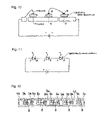
- FIG. 16 is a front view
- FIG. 17 is a cross-sectional view taken along line A-A of FIG. 16 .
- the light emitting devices B of FIG. 2 (light emitting device 59 of FIG. 15 ) are mounted instead of the light emitting devices C of FIG. 3 , thus differentiating the device of FIGS. 16 and 17 from the above-described light emitting semiconductor apparatus of FIGS. 14 and 15 .
- the light emitting devices 56 , 59 are electrically connected in series. When a voltage is applied across a pair of the external connection terminals 55 that are led out of the lamp house 51 and located along the outer circumferential surface of the lamp house 51 , all the light emitting devices 56 , 59 are driven to emit light.
- the light emitting device C has the direction characteristic shown in FIG. 6 and the light emitting device B has the direction characteristic shown in FIG. 5 .
- the two types of light emitting semiconductor apparatus of the conventional/related art which contain such light emitting devices also have the direction characteristics shown in FIGS. 15 and 17 , respectively.
- the direction characteristics of the light emitting semiconductor apparatus of FIG. 15 which contains the plurality of light emitting devices C includes a region between adjacent light emitting devices C where light distributions thereof overlap widely, as shown.
- the presence of such a light distribution overlap region causes the following problem when incorporated into a light emitting semiconductor apparatus.
- the overlap region receives a larger amount of light emitted from the light emitting device C than other regions such as a region in the vicinity of the optical axis of the light emitting device C.
- the overlap region also receives a larger amount of light that is wavelength-converted by the phosphor contained in the sealing resin and covering the light emitting device C, in comparison with other regions.
- the apparatus uses a phosphor that can wavelength-convert the blue light into a complementary color yellow light when excited by the blue light to obtain a light chromatically near a white light
- a bluish white light is released from an area where the light emitting device C is located. This is because the area has a stronger light source color received from the light emitting device C.
- a yellowish white light is released from an area between the light emitting devices C because the area has a stronger wavelength-converted light.
- the light emitting semiconductor apparatus exhibits color unevenness.
- the phosphor and the light transmissive resin contained in the sealing resin which are topically irradiated with the blue light having relatively higher energy among the various light rays, will deteriorate faster than the light transmissive resin and the phosphor in other regions.
- the deterioration of the light transmissive resin over time causes a reduction in the transmissivity of the resin and a variation in color.
- the deterioration of the phosphor over time causes a reduction in the wavelength conversion efficiency of the phosphor.
- various problems arise over time associated with the topical deterioration and with respect to the amount and chromaticity of the illuminating light.
- the direction characteristic of the light emitting semiconductor apparatus of FIG. 17 which includes light emitting devices B also includes a region between adjacent light emitting devices B where light distributions thereof widely overlap, as shown.
- a light emitting semiconductor apparatus is disclosed that can achieve reduced color unevenness associated with an illuminating light and can have a quality of suppressed topical deterioration over time of the amount and chromaticity of the illuminating light.
- a light emitting semiconductor apparatus can include a plurality of light emitting semiconductor devices mounted on a substrate, wherein the light emitting semiconductor devices are sealed in a light transmissive resin containing a phosphor.
- the light emitting semiconductor devices can have at least two types of different direction characteristics, and the light emitting semiconductor devices having different direction characteristics are arrayed adjacent to each other.
- two types of direction characteristics can include one in the form of a substantial cone shape having a bottom adjacent to the light emitting semiconductor device, and another in the form of a substantial reverse cone having an apex adjacent to the light emitting semiconductor device.
- an odd number of light emitting semiconductor devices can be arranged in line.
- the light emitting semiconductor devices can be arranged in a matrix with an odd number of rows and an odd number of columns, the rows and the columns each including an odd number of light emitting semiconductor devices.
- the light emitting semiconductor devices located at both ends in the case of an in-line arrangement have a direction characteristic in the form of a substantial cone.
- the light emitting semiconductor devices located at corners in the case of the matrix arrangement have a direction characteristic in the form of a substantial cone.
- the plurality of light emitting semiconductor devices can have N-electrodes and P-electrodes connected alternately through die bonding or wire bonding, wherein the electrodes on adjacent light emitting semiconductor devices, if not connected through die bonding, are connected to each other through wire bonding.
- FIG. 1 is a perspective view of a light emitting semiconductor device.
- FIG. 2 is a perspective view of another light emitting semiconductor device.
- FIG. 3 is a perspective view of yet another light emitting semiconductor device.
- FIG. 4 shows a direction characteristic of the light emitting semiconductor device of FIG. 1 .
- FIG. 5 shows a direction characteristic of the light emitting semiconductor device of FIG. 2 .
- FIG. 6 shows a direction characteristic of the light emitting semiconductor device of FIG. 3 .
- FIG. 7 is a front view of an exemplary embodiment of a light emitting semiconductor apparatus made in accordance with principles of the disclosed subject matter.
- FIG. 8 is a cross-sectional view taken along line A-A of FIG. 7 .
- FIG. 9 is an illustrative view of light emitting semiconductor devices mounted for the apparatus of FIG. 7 .
- FIG. 10 is another illustrative view of light emitting semiconductor devices mounted for the apparatus of FIG. 7 .
- FIG. 11 is an internal wiring diagram for the apparatus of FIG. 7 .
- FIG. 12 is a plan view of another exemplary embodiment of a light emitting semiconductor apparatus made in accordance with principles of the disclosed subject matter.
- FIG. 13 is a plan view of another exemplary embodiment of a light emitting semiconductor apparatus made in accordance with principles of the disclosed subject matter.
- FIG. 14 is a front view of a conventional/related art semiconductor apparatus.
- FIG. 15 is a cross-sectional view taken along line A-A of FIG. 14 .
- FIG. 16 is a front view of another conventional/related art semiconductor apparatus.
- FIG. 17 is a cross-sectional view taken along line A-A of FIG. 16 .
- FIGS. 1-13 wherein the same or similar parts are denoted with the same reference numerals.
- the below-described embodiments are specific examples of the disclosed subject matter and are given various technical features. However, the disclosed subject matter is not limited to these embodiments.
- FIG. 7 is a front view of an example of a light emitting semiconductor device made in accordance with principles of the disclosed subject matter.
- FIG. 8 is a cross-sectional view taken along line A-A of FIG. 7 .
- FIGS. 9 and 10 are illustrative views of mounted light emitting semiconductor devices for this example.
- FIG. 11 is an internal wiring diagram for the device shown in FIG. 7 .
- a lamp house 1 composed of a resinous member and a substrate (lead frames 2 a , 2 b , 2 c ) composed of a metallic member are integrated through insert molding.
- the lamp house 1 has a recess 5 with an aperture 4 .
- the recess 5 has an inner bottom, through which bonding pads 6 a , 6 b , 6 c are exposed in line on respective ends of three separate lead frames 2 a , 2 b , 2 c .
- the bonding pads 2 b , 2 c form a pair located in an outermost position and extend through the lamp house 1 and lead out of the outer circumferential surface of the lamp house 1 to an external area to form a pair of external connection terminals 7 b , 7 c on the other end of the lead frames 2 b , 2 c .
- the terminals 7 b , 7 c are located along the outer circumferential surface of the lamp house 1 .
- three light emitting devices 3 a , 3 b and 3 b are used.
- the light emitting devices 3 a and 3 b are the same in material and structure (equal in light emission spectral distribution) but different in direction characteristic.
- the light emitting device may have either the direction characteristic of a substantial reverse conical form, as shown in FIG. 5 , or the direction characteristic of a substantial conical form, as shown in FIG. 6 .
- the centrally located bonding pad 6 a is die-bonded to two light emitting devices 3 a , 3 b .
- one of the bonding pads 6 b , 6 c of the outermost pair, or the bonding pad 6 b is die-bonded to one light emitting device 3 b .
- No light emitting device is mounted on the bonding pad 6 c .
- the two light emitting devices 3 a , 3 b mounted on the centrally located bonding pad 6 a include the light emitting device 3 b mounted closer to the bonding pad 6 c .
- a wire bonding electrode on that light emitting device 3 b is wire-bonded via a bonding wire 8 to the bonding pad 6 c to establish electrical conduction therebetween.
- the light emitting device 3 a located on the pad 6 a and the light emitting device 3 b located on the pad 6 b have respective wire bonding electrodes thereon, which can be stitch-bonded via a bonding wire 8 to each other to establish electrical conduction therebetween.
- the two light emitting devices 3 a , 3 b mounted on the centrally located bonding pad 6 a have respective die bonding electrodes, which are die-bonded to the bonding pad 6 a to establish electrical conduction therebetween.
- the light emitting semiconductor apparatus of the present example has internal wiring, which can be formed in a serial circuit as shown in FIG. 11 .
- the light emitting devices 3 a , 3 b can have the same material and structure and almost the same size. Therefore, a P-electrode (anode electrode) and an N-electrode (cathode electrode) can be formed on both the die bonding side and the wire bonding side.
- the die bonding side may be used as the N-electrode and the wire bonding side as the P-electrode.
- the die bonding side may be used as the P-electrode and the wire bonding side as the N-electrode.
- the light emitting device using the die bonding side as the N-electrode (and the wire bonding side as the P-electrode) and the light emitting device using the die bonding side as the P-electrode (and the wire bonding side as the N-electrode) are mounted alternately as shown in FIGS. 9 and 10 .
- the light emitting device 3 b having the direction characteristic of a substantial conical form is mounted at an outermost position, and the light emitting device 3 b having the direction characteristic of a substantial conical form and the light emitting device 3 a having the direction characteristic of a substantial reverse conical form are mounted alternately as shown in FIG. 8 .
- the light emitting device 3 a having the direction characteristic of a substantial reverse conical form may use a light emitting device that has an output peak at 45°-75° as shown in FIG. 5 .
- the light emitting device 3 b having the direction characteristic of a substantial conical form may use a light emitting device that has an output peak at a higher angle (close to the horizontal direction) than that of the light emitting device having the direction characteristic of a substantial reverse conical form.
- a light emitting device can be used that has an output peak at near 80°-90°.
- a light emitting device that has an output peak at 0° (in the normal direction) or near 0°-30° may be used.
- the light passing through the phosphor-mixed light transmissive resin in that area topically increases and easily causes a variation in chromaticity. Therefore, it is difficult to reduce the phosphor concentration.
- a light emitting device having an output peak in the normal direction is not always preferable. Accordingly, a light emitting device that has an output peak at a higher angle (closer to the horizontal direction) than 45° can be used to avoid the above problems.
- a light emitting device that has an output peak at near 60° is suitable.
- the recess 5 can be filled with a sealing resin 9 that includes a light transmissive resin containing one or more types of phosphors to seal the light emitting devices 3 a , 3 b , 3 b and the bonding wires 8 in resin.
- the light transmissive resin contained in the sealing resin 9 is functional to protect the light emitting devices 3 a , 3 b , 3 b from external environments such as moisture, dusts and gases and to protect the bonding wires 8 from external forces such as vibrations and impacts.
- the light exit surfaces of the light emitting devices 3 a , 3 b , 3 b form interfaces with the sealing resin 9 .
- the refractive index of the sealing resin 9 that forms interfaces with the light exit surfaces of the light emitting devices 3 a , 3 b , 3 b can be configured to be closer to that of the semiconductor material that forms the light exit surfaces of the light emitting devices 3 a , 3 b , 3 b .
- the light transmissive resin also serves to improve the efficiency of extraction of the light emitted from the light exit surfaces of the light emitting devices 3 a , 3 b , 3 b and which is led into the sealing resin 9 .
- a certain voltage is applied across a pair of the external connection terminals 7 b , 7 c located along the outer circumferential surface of the lamp house 1 .
- three serially connected light emitting devices 3 a , 3 b , 3 b initiate emission of light.
- the light emitted from the three light emitting devices 3 a , 3 b , 3 b form the direction characteristics shown with phantom lines in FIG. 8 .
- the wavelength-converted light from the phosphor is guided through the sealing resin 9 and released externally.
- the apparatus may use a phosphor that can wavelength-convert the blue light into a complementary color yellow light when excited by the blue light.
- the yellow light that results from the wavelength-conversion of the blue light emitted from the light emitting devices 3 a , 3 a , 3 b and the blue light emitted from the light emitting devices are subjected to additional color mixture to obtain a light chromatically near a white light.
- the apparatus may use two types of phosphors in mixture that can wavelength-convert the blue light into a green and a red light when excited by the blue light.
- the resulting green and red lights and the blue light emitted from the light emitting devices 3 a , 3 a , 3 b can be subjected to additional color mixture to obtain a light chromatically almost equal to a white light.
- the apparatus may use three types of phosphors in mixture that can wavelength-convert the ultraviolet light into a blue, a green and a red light.
- the blue, green and red lights can be subjected to additional color mixture to obtain a light chromatically almost equal to a white light.
- the light emitted from the light emitting devices 3 a , 3 b , 3 b and the phosphors may be mixed appropriately to obtain various chromatic lights such as a light almost equal to a white light or a light other than a light chromatically near white light.
- the shape of the light emitting device can be changed to control the direction characteristic of the light emitting device.
- the shape and/or size of the electrode in particular, the electrode on the wire bonding side
- the shape of the light emitting device and the shape and/or size of the electrode may be changed at the same time to control the direction characteristic.
- the light emitting device 3 b that has the direction characteristic of a substantial conical form is mounted at an outermost location.
- the light emitting device 3 b that has a direction characteristic of a substantial conical form and the light emitting device 3 a that has a direction characteristic of a substantial reverse conical form are mounted alternately. As a result, a light distribution can be obtained as shown in FIG. 8 .
- This light distribution has an comparatively smaller region where the light distributions of the adjacent light emitting devices 3 a , 3 b overlap, in comparison with that of the light emitting semiconductor apparatus of the conventional art shown in FIGS. 15 and 17 .
- the light emitted from the light emitting devices 3 a , 3 b can be released almost uniformly within the sealing resin 9 .
- the phosphor and the light transmissive resin contained in the sealing resin 9 of the light emitting semiconductor apparatus can have a uniform deterioration rate over the entire zone. In this case, less variation arises in brightness and chromaticity regardless of the cumulative elapsed drive time for the light emitting semiconductor apparatus.
- the light emitting device 3 b having a direction characteristic of a substantial conical form is mounted at an outermost location. Accordingly, a region that receives a smaller amount of light from the light emitting devices 3 a , 3 b (as in the light distribution of the light emitting semiconductor apparatus shown in FIG. 15 ) is hardly present in the above-described embodiment. Therefore, the phosphor dispersed within the sealing resin 9 can be exited almost uniformly over the entire zone. This is effective to realize a light emitting semiconductor apparatus with less variation in chromaticity.
- the amount of light that is wavelength-converted by the phosphor dispersed within a region and that receives a smaller amount of light from the light emitting device can be used as a reference to determine the concentration of the phosphor mixed in the light transmissive resin. Accordingly, in order to ensure a certain amount of light that is wavelength-converted in the region, the concentration of the phosphor mixed in the light transmissive resin is determined to be higher.
- the phosphor dispersed within the sealing resin 9 can be excited over the entire zone. Therefore, even if the concentration of the phosphor mixed in the light transmissive resin is determined to be lower than that in the light emitting semiconductor apparatus of the conventional/related art, it is possible to achieve an illuminating light of chromaticity corresponding to that of the light emitting semiconductor apparatus of the conventional/related art. Accordingly, usage of the phosphor can be reduced and the material expense can correspondingly be saved.
- a test calculation expects to achieve about a 20-30% reduction in phosphor relative to the light emitting semiconductor apparatus of the conventional/related art.
- the phosphor has the function of wavelength converting the exciting light and the nature of absorbing and scattering part of the light, as described above. Accordingly, most of the light absorbed and scattered is converted into heat and not externally released. Therefore, a higher concentration of phosphor results in a lower brightness of the light emitting semiconductor apparatus.
- the above-described example makes it possible to reduce the concentration of phosphor, which can provide the light emitting semiconductor apparatus with higher brightness.
- the higher brightness results in a reduction in energy requirements.
- the light emitting semiconductor apparatus containing a plurality of light emitting devices 3 a , 3 b , 3 b serially connected through inner wiring can be realized as follows. Namely, the light emitting device having an N-electrode on the die bonding side (and the P-electrode on the wire bonding side) and the light emitting device having a P-electrode on the die bonding side (and the N-electrode on the wire bonding side) are alternately mounted.
- the light emitting device having an N-electrode on the die bonding side (and a P-electrode on the wire bonding side) and the light emitting device having a P-electrode on the die bonding side (and an N-electrode on the wire bonding side) are die-bonded to the common bonding pad 6 a .
- the light emitting devices 3 a , 3 b mounted respectively on the adjacent bonding pads 6 a , 6 b are stitch-bonded to each other via a bonding wire 8 to establish electrical connection between the bonding pads 6 a , 6 b .
- the lead frame is generally molded through a process of pressing with a mold. Therefore, the structure of the mold can be simplified and the mold expense can be reduced.
- FIG. 12 is a plan view of another exemplary embodiment of a light emitting semiconductor apparatus made in accordance with principles of the disclosed subject matter.
- the present example includes an increased number of light emitting semiconductor devices to be mounted, which is different from the above-described example 1.
- each of the bonding pads 6 a receives the light emitting semiconductor devices 3 a and 3 b mounted thereon.
- the bonding pad 6 b can be configured to receive only the light emitting semiconductor device 3 a mounted thereon.
- the bonding pad 6 c of this example receives no light emitting semiconductor device mounted thereon.
- the light emitting devices 3 b having the direction characteristic of the almost conical form are mounted on both outermost sides.
- the light emitting devices 3 b having a direction characteristic of a substantial conical form and the light emitting device 3 a having a direction characteristic of a substantial reverse conical form can be alternately mounted.
- a plurality (odd number) of light emitting devices 3 a , 3 b are mounted and internally wired in series to realize a light emitting semiconductor apparatus.
- the light emitting device having the N-electrode on the die bonding side (and the P-electrode on the wire bonding side) and the light emitting device having the P-electrode on the die bonding side (and the N-electrode on the wire bonding side) are alternately mounted.
- the light emitting device having an N-electrode on the die bonding side (and a P-electrode on the wire bonding side) and the light emitting device having a P-electrode on the die bonding side (and an N-electrode on the wire bonding side) are die-bonded to the common bonding pad 6 a .
- a plurality of such bonding pads 6 a can be arranged in line.
- the light emitting devices 3 a , 3 b mounted respectively on the adjacent bonding pads 6 a are stitch-bonded to each other via a bonding wire 8 to establish electrical connection between the adjacent bonding pads 6 a .
- the light emitting device 3 a located closer to the bonding pad 6 b on the bonding pad 6 a adjacent to the bonding pad 6 b is connected via a bonding wire 8 to the light emitting device 3 b on the bonding pad 6 b .
- the light emitting device 3 b located closer to the bonding pad 6 c on a bonding pad 6 a located adjacent to the bonding pad 6 c is connected via a bonding wire 8 to the bonding pad 6 c.
- the present example has the same basic arrangement as that of the example shown in FIG. 7 and accordingly exerts the similar effect and functions.
- the light emitting semiconductor apparatus of the above-described exemplary embodiment exhibits enhanced effects as compared to the light emitting semiconductor apparatus of the conventional/related art as the number of the mounted light emitting devices increases.
- W is the number of bonding wires and n is the number of semiconductor light emitting devices. Therefore, as compared to the light emitting semiconductor apparatus of the conventional/related art, (n ⁇ 3)/2 bonding wires, can be saved.
- FIG. 13 is a plan view of another exemplary embodiment associated with the light emitting semiconductor apparatus of the disclosed subject matter.
- the present example includes a plurality of light emitting semiconductor devices 3 a , 3 b mounted in matrix. Also in this case, similar to the above examples of FIGS. 7 and 12 , the light emitting devices 3 a , 3 b are internally wired in series in the light emitting semiconductor apparatus. In this case, the light emitting device having an N-electrode on the die bonding side (and a P-electrode on the wire bonding side) and the light emitting device having a P-electrode on the die bonding side (and an N-electrode on the wire bonding side) are alternately mounted in turn based on wiring.
- the light emitting device having an N-electrode on the die bonding side (and a P-electrode on the wire bonding side) and the light emitting devices 3 a , 3 b having a P-electrode on the die bonding side (and an N-electrode on the wire bonding side) are die-bonded to the common bonding pad 6 a .
- a plurality of such bonding pads 6 a are arranged in a plane.
- the light emitting devices 3 a , 3 b mounted respectively on adjacent bonding pads 6 a are stitch-bonded to each other via a bonding wire 8 to establish electrical connection between the bonding pads 6 a .
- the bonding pad 6 b includes only the light emitting semiconductor device 3 b mounted thereon.
- the bonding pad 6 c includes no light emitting semiconductor device mounted thereon.
- the electrical connections associated with the bonding pads 6 b , 6 c and the light emitting devices 3 a , 3 b can be the same as those in the examples described with respect to FIGS. 7 and 12 .
- a light emitting semiconductor device 3 b having a direction characteristic of a substantial conical form can be mounted at each corner of the matrix.
- the light emitting device 3 b having a direction characteristic of a substantial conical form and the light emitting device 3 a having a direction characteristic of a substantial reverse conical form are alternately mounted .
- the light emitting semiconductor devices having different direction characteristics can be arrayed adjacent to each other. In the case of this matrix arrangement, though, the light emitting semiconductor devices located diagonally adjacent to each other (in a slanting direction) do not match the definition of “adjacent to each other” in the presently disclosed subject matter.
- the present example includes the light emitting devices 3 a , 3 b mounted in plane and the effects achieved thereby can reflect those of the previously described embodiments of the disclosed subject matter.
- most of the aerial wiring using bonding wires is achieved by stitch bonding. Accordingly, the number of bonding pads that receive the light emitting devices mounted thereon can be reduced. In addition, the number of pads for wire bonding can be reduced to one or two. Further, the arrangement area for the light emitting device requires no lead for wiring that extends from the bonding pad. As a result, it is possible to narrow the interval between the light emitting devices mounted in matrix and realize a downsized light emitting semiconductor apparatus with a reduced mounting area for the light emitting device.
- the light emitting semiconductor apparatus of the disclosed subject matter is usable as light sources in various fields such as LCD back-lights, reading light sources for printers, panel illuminators, general illuminators, light sources for vehicular lamps, various indicators, etc.
Landscapes
- Engineering & Computer Science (AREA)
- Power Engineering (AREA)
- Microelectronics & Electronic Packaging (AREA)
- Physics & Mathematics (AREA)
- Condensed Matter Physics & Semiconductors (AREA)
- General Physics & Mathematics (AREA)
- Computer Hardware Design (AREA)
- Led Device Packages (AREA)
Applications Claiming Priority (2)
| Application Number | Priority Date | Filing Date | Title |
|---|---|---|---|
| JP2006-125765 | 2006-04-28 | ||
| JP2006125765A JP4863203B2 (ja) | 2006-04-28 | 2006-04-28 | 半導体発光装置 |
Publications (2)
| Publication Number | Publication Date |
|---|---|
| US20070262340A1 US20070262340A1 (en) | 2007-11-15 |
| US7592640B2 true US7592640B2 (en) | 2009-09-22 |
Family
ID=38542571
Family Applications (1)
| Application Number | Title | Priority Date | Filing Date |
|---|---|---|---|
| US11/739,877 Expired - Fee Related US7592640B2 (en) | 2006-04-28 | 2007-04-25 | Light emitting semiconductor apparatus |
Country Status (6)
| Country | Link |
|---|---|
| US (1) | US7592640B2 (ko) |
| JP (1) | JP4863203B2 (ko) |
| KR (1) | KR101274403B1 (ko) |
| CN (1) | CN101064301B (ko) |
| DE (1) | DE102007020011B4 (ko) |
| TW (1) | TWI467794B (ko) |
Families Citing this family (9)
| Publication number | Priority date | Publication date | Assignee | Title |
|---|---|---|---|---|
| US20080175009A1 (en) * | 2007-01-19 | 2008-07-24 | Unity Opto Technology Co., Ltd. | Edge-emitting light-emitting diode |
| US9041042B2 (en) | 2010-09-20 | 2015-05-26 | Cree, Inc. | High density multi-chip LED devices |
| JP5340763B2 (ja) * | 2009-02-25 | 2013-11-13 | ローム株式会社 | Ledランプ |
| JP5793685B2 (ja) * | 2011-04-18 | 2015-10-14 | パナソニックIpマネジメント株式会社 | 発光装置、バックライトユニット、液晶表示装置及び照明装置 |
| KR101941030B1 (ko) * | 2011-08-24 | 2019-01-22 | 엘지이노텍 주식회사 | 발광소자 패키지 |
| JP6326830B2 (ja) * | 2013-02-28 | 2018-05-23 | 日亜化学工業株式会社 | 発光装置及びそれを備える照明装置 |
| USD780704S1 (en) * | 2014-08-27 | 2017-03-07 | Mitsubishi Electric Corporation | Light source module |
| USD768584S1 (en) * | 2014-11-13 | 2016-10-11 | Mitsubishi Electric Corporation | Light source module |
| JP2022107942A (ja) * | 2021-01-12 | 2022-07-25 | シーシーエス株式会社 | Led光源 |
Citations (1)
| Publication number | Priority date | Publication date | Assignee | Title |
|---|---|---|---|---|
| JP2005285874A (ja) | 2004-03-26 | 2005-10-13 | Kyocera Corp | 発光素子収納用パッケージおよび発光装置ならびに照明装置 |
Family Cites Families (10)
| Publication number | Priority date | Publication date | Assignee | Title |
|---|---|---|---|---|
| JPS5324294A (en) * | 1976-08-19 | 1978-03-06 | Matsushita Electric Ind Co Ltd | Light source for information reader |
| JP3571477B2 (ja) * | 1996-12-06 | 2004-09-29 | ローム株式会社 | 半導体発光素子 |
| US6229160B1 (en) * | 1997-06-03 | 2001-05-08 | Lumileds Lighting, U.S., Llc | Light extraction from a semiconductor light-emitting device via chip shaping |
| US6577073B2 (en) * | 2000-05-31 | 2003-06-10 | Matsushita Electric Industrial Co., Ltd. | Led lamp |
| EP2241803B1 (en) * | 2001-05-26 | 2018-11-07 | GE Lighting Solutions, LLC | High power LED-lamp for spot illumination |
| JP4561954B2 (ja) * | 2003-08-08 | 2010-10-13 | 東芝ライテック株式会社 | 発光装置 |
| JP2005158958A (ja) * | 2003-11-25 | 2005-06-16 | Matsushita Electric Works Ltd | 発光装置 |
| US20080290354A1 (en) * | 2004-07-27 | 2008-11-27 | Koninklijke Philips Electronics, N.V. | Light Emitting Diode Assembly |
| JP3875247B2 (ja) * | 2004-09-27 | 2007-01-31 | 株式会社エンプラス | 発光装置、面光源装置、表示装置及び光束制御部材 |
| KR100867970B1 (ko) * | 2004-10-04 | 2008-11-11 | 가부시끼가이샤 도시바 | 발광 장치 및 그것을 이용한 조명 기구 또는 액정표시장치 |
-
2006
- 2006-04-28 JP JP2006125765A patent/JP4863203B2/ja not_active Expired - Fee Related
-
2007
- 2007-03-26 TW TW96110427A patent/TWI467794B/zh not_active IP Right Cessation
- 2007-04-23 KR KR1020070039322A patent/KR101274403B1/ko not_active IP Right Cessation
- 2007-04-25 US US11/739,877 patent/US7592640B2/en not_active Expired - Fee Related
- 2007-04-27 DE DE102007020011.2A patent/DE102007020011B4/de active Active
- 2007-04-27 CN CN2007101019289A patent/CN101064301B/zh not_active Expired - Fee Related
Patent Citations (1)
| Publication number | Priority date | Publication date | Assignee | Title |
|---|---|---|---|---|
| JP2005285874A (ja) | 2004-03-26 | 2005-10-13 | Kyocera Corp | 発光素子収納用パッケージおよび発光装置ならびに照明装置 |
Also Published As
| Publication number | Publication date |
|---|---|
| KR101274403B1 (ko) | 2013-06-14 |
| JP2007299879A (ja) | 2007-11-15 |
| KR20070106409A (ko) | 2007-11-01 |
| TWI467794B (zh) | 2015-01-01 |
| DE102007020011A1 (de) | 2007-10-31 |
| JP4863203B2 (ja) | 2012-01-25 |
| CN101064301B (zh) | 2010-11-10 |
| DE102007020011B4 (de) | 2017-10-26 |
| CN101064301A (zh) | 2007-10-31 |
| TW200742137A (en) | 2007-11-01 |
| US20070262340A1 (en) | 2007-11-15 |
Similar Documents
| Publication | Publication Date | Title |
|---|---|---|
| US7592640B2 (en) | Light emitting semiconductor apparatus | |
| JP4679183B2 (ja) | 発光装置及び照明装置 | |
| US7906892B2 (en) | Light emitting device | |
| JP4077170B2 (ja) | 半導体発光装置 | |
| US7759683B2 (en) | White light emitting diode | |
| JP5379634B2 (ja) | Ledパッケージモジュール | |
| US6881980B1 (en) | Package structure of light emitting diode | |
| US20070001188A1 (en) | Semiconductor device for emitting light and method for fabricating the same | |
| US8450770B2 (en) | Light emitting package structure | |
| US8132934B2 (en) | Light emitting device and light unit having the same | |
| US9224720B2 (en) | Light-emitting device including light-emitting diode element that is mounted on outer portion of electrode | |
| EP2738825A1 (en) | Light-emitting device | |
| US20080123367A1 (en) | Light source unit for use in a backlight module | |
| US20110089815A1 (en) | Light-emitting device | |
| US8421102B2 (en) | Semiconductor light-emitting device having a member in a periphery made of a material whose color, transparency or adhesiveness changes overtime due to light or heat emission from the emitting element | |
| JP2006310613A (ja) | 半導体発光装置 | |
| JP2006351708A (ja) | 発光ダイオードランプ及び光源装置 | |
| TW201525525A (zh) | 光學顯示系統 | |
| JP2018129492A (ja) | 発光装置、及び、照明装置 | |
| JP2012009793A (ja) | 発光装置、バックライトユニット、液晶表示装置及び照明装置 | |
| KR101518459B1 (ko) | Led 패키지 | |
| JP2017117853A (ja) | 発光装置、及び、照明装置 | |
| JP2007274009A5 (ko) | ||
| KR20080088218A (ko) | 색 편차를 줄인 발광 다이오드 패키지 | |
| JP2005285920A (ja) | Led |
Legal Events
| Date | Code | Title | Description |
|---|---|---|---|
| AS | Assignment |
Owner name: STANLEY ELECTRIC CO., LTD., JAPAN Free format text: ASSIGNMENT OF ASSIGNORS INTEREST;ASSIGNORS:SUMI, KAZUNORI;AOKI, DAI;REEL/FRAME:019309/0835 Effective date: 20070510 |
|
| STCF | Information on status: patent grant |
Free format text: PATENTED CASE |
|
| FEPP | Fee payment procedure |
Free format text: PAYOR NUMBER ASSIGNED (ORIGINAL EVENT CODE: ASPN); ENTITY STATUS OF PATENT OWNER: LARGE ENTITY |
|
| FPAY | Fee payment |
Year of fee payment: 4 |
|
| FPAY | Fee payment |
Year of fee payment: 8 |
|
| FEPP | Fee payment procedure |
Free format text: MAINTENANCE FEE REMINDER MAILED (ORIGINAL EVENT CODE: REM.); ENTITY STATUS OF PATENT OWNER: LARGE ENTITY |
|
| LAPS | Lapse for failure to pay maintenance fees |
Free format text: PATENT EXPIRED FOR FAILURE TO PAY MAINTENANCE FEES (ORIGINAL EVENT CODE: EXP.); ENTITY STATUS OF PATENT OWNER: LARGE ENTITY |
|
| STCH | Information on status: patent discontinuation |
Free format text: PATENT EXPIRED DUE TO NONPAYMENT OF MAINTENANCE FEES UNDER 37 CFR 1.362 |
|
| FP | Lapsed due to failure to pay maintenance fee |
Effective date: 20210922 |