US7220347B2 - Electrolytic copper plating bath and plating process therewith - Google Patents
Electrolytic copper plating bath and plating process therewith Download PDFInfo
- Publication number
- US7220347B2 US7220347B2 US11/181,856 US18185605A US7220347B2 US 7220347 B2 US7220347 B2 US 7220347B2 US 18185605 A US18185605 A US 18185605A US 7220347 B2 US7220347 B2 US 7220347B2
- Authority
- US
- United States
- Prior art keywords
- blind via
- plating
- leveler
- holes
- hole
- Prior art date
- Legal status (The legal status is an assumption and is not a legal conclusion. Google has not performed a legal analysis and makes no representation as to the accuracy of the status listed.)
- Active, expires
Links
- 0 Cl.Cl.[1*]N1=CN(C([H])(C)C([H])([H])C)C=C1.[2*]N1=CN(C([H])(C)C([H])([H])C)C=C1.[H]C([H])(C)C([H])(C)N1CCCC1=O Chemical compound Cl.Cl.[1*]N1=CN(C([H])(C)C([H])([H])C)C=C1.[2*]N1=CN(C([H])(C)C([H])([H])C)C=C1.[H]C([H])(C)C([H])(C)N1CCCC1=O 0.000 description 10
- GRAILFVLBRMAIR-UHFFFAOYSA-J CCOC(=S)SCCCS(=O)(=O)O[K].CN(C)C(=S)SCCCS(=O)(=O)O[Na].O=S(=O)(CCCSSCCCS(=O)(=O)O[Na])O[Na].O=S(=O)(O)OCCCSSCCCOS(=O)(=O)O Chemical compound CCOC(=S)SCCCS(=O)(=O)O[K].CN(C)C(=S)SCCCS(=O)(=O)O[Na].O=S(=O)(CCCSSCCCS(=O)(=O)O[Na])O[Na].O=S(=O)(O)OCCCSSCCCOS(=O)(=O)O GRAILFVLBRMAIR-UHFFFAOYSA-J 0.000 description 1
Images


Classifications
-
- C—CHEMISTRY; METALLURGY
- C25—ELECTROLYTIC OR ELECTROPHORETIC PROCESSES; APPARATUS THEREFOR
- C25D—PROCESSES FOR THE ELECTROLYTIC OR ELECTROPHORETIC PRODUCTION OF COATINGS; ELECTROFORMING; APPARATUS THEREFOR
- C25D3/00—Electroplating: Baths therefor
- C25D3/02—Electroplating: Baths therefor from solutions
- C25D3/38—Electroplating: Baths therefor from solutions of copper
-
- H—ELECTRICITY
- H05—ELECTRIC TECHNIQUES NOT OTHERWISE PROVIDED FOR
- H05K—PRINTED CIRCUITS; CASINGS OR CONSTRUCTIONAL DETAILS OF ELECTRIC APPARATUS; MANUFACTURE OF ASSEMBLAGES OF ELECTRICAL COMPONENTS
- H05K3/00—Apparatus or processes for manufacturing printed circuits
- H05K3/40—Forming printed elements for providing electric connections to or between printed circuits
- H05K3/42—Plated through-holes or plated via connections
- H05K3/423—Plated through-holes or plated via connections characterised by electroplating method
Definitions
- the present invention relates to an electrolytic copper plating bath and a plating process therewith which show excellent filling properties in plating of a substrate having blind via-holes with small diameter and high aspect ratio and which are suitable also for performing via-filling plating and through-hole plating simultaneously for a substrate having both blind via-holes and through-holes.
- a plating accelerator called a brightener which is a sulfur-containing organic substance
- plating suppressors called a carrier which is a polyether compound and a leveler which is a nitrogen-containing compound.
- the brighteners are comparatively higher in diffusion rate, whereas the carriers and levelers are comparatively lower in diffusion rate.
- the blind via-holes to be filled up have had a large diameter of 50 ⁇ m or more and a low aspect ratio of 1 or less; thus, the blind via-holes have been comparatively flat in shape.
- the blind via-holes to be filled up have come to have a smaller diameter and a higher aspect ratio.
- the blind via-holes for the purpose of forming through-electrodes have a small diameter of several micrometers to several tens of micrometers and a depth of about 100 ⁇ m; thus, there is a demand for filling up the blind via-hole with a high aspect ratio by a via-filling plating process.
- the absolute value of hole depth has been about 1 ⁇ m, though the aspect ratio has been high.
- the blind via-holes have a smaller aperture diameter or a large depth
- the potential difference between the substrate surface side and a bottom portion of the blind via-hole is large, so that the current distribution in the inside of the blind via-hole would be worsened. Therefore, where there is no effect of additive, deposition near the surface is more vigorous than deposition in the bottom portion, so that a cavity is generated, and the blind via-holes cannot be filled up with the copper plating film.
- FIG. 1 shows a schematic diagram for illustrating the potential and diffusion layer conditions in via-filling.
- the via-filling is performed the difference in diffusion rate between the leveler and the brightener.
- the leveler is lower than the brightener in diffusion rate, so that the leveler is supplied to the substrate surface and the blind via-hole surface side where the diffusion layer is thinner, thereby suppressing the plating.
- the supply of the leveler cannot catch up with the supply of the brightener on the blind via-hole bottom side where the diffusion layer is thicker, so that the plating-accelerating effect predominates there.
- the plating film preferentially grows starting from the blind via-hole bottom side, whereby the blind via-holes are filled up.
- the use of a leveler e.g., Janus green or the like
- a leveler effective for via-filling plating in the cases of blind via-holes having a low aspect ratio according to the conventional art results in that, since the diffusion rate of the leveler is too low, even a slight thickening of the diffusion layer (toward that on the blind via-hole bottom side) on the substrate surface side of the blind via-holes causes the leveler supply to be insufficient, and a sufficient plating suppression cannot be obtained.
- the plating film grows faster than at the blind via-hole bottom portion, resulting in the formation of a cavity in the vicinity of the blind via-hole bottom portion.
- the blind via-holes can be filled up, but, in the through-hole, the plating suppression of the leveler is concentrated on the through-hole corner area where the diffusion layer is thinnest, with the result of formation of a thinner plating film in this area.
- This condition as it is, is accompanied by a considerably bad reliability of conduction; to cope with this problem, therefore, further time and steps would be required, i.e., the plating process may take a longer time, or a treatment for making the substrate conductive may be needed.
- the present invention has been made in consideration of the above-mentioned circumstances. Accordingly, it is an object of the prevent invention to provide an electrolytic copper plating bath and a plating process therewith which show excellent filling properties in plating of a substrate having blind via-holes with small diameter and high aspect ratio and which are suitable also for performing via-filling plating and through-hole plating simultaneously for a substrate having both blind via-holes and through-holes.
- the present inventor has made intensive and extensive investigations for solving the above-mentioned problems, and, as a result of the investigations, has found that, when via-filling plating for blind via-holes formed on a substrate is carried out by use of an electrolytic copper plating bath containing a water-soluble copper salt, sulfuric acid, chloride ions, and a leveler as an additive, wherein the leveler is either one or both of a quaternary polyvinylimidazolium compound represented by the following formula (1), and a copolymer, represented by the following formula (2), of a vinylpyrrolidone and a quaternary vinylimidazolium compound:
- the electrolytic copper plating bath further containing a brightener and/or a carrier wherein the brightener is at least one selected from the group consisting of sulfur-containing additives represented by the following formulas (3) to (6):
- R 3 , R 4 and R 5 are each an alkyl group of 1 to 5 carbon atoms
- M is a hydrogen atom or an alkali metal
- a is an integer of 1 to 8
- b, c and d are each 0 or 1
- the carrier is a polyalkylene glycol represented by the following formula (7): HO—(R 6 —O) e —H (7) where R 6 is an alkylene group of 2 or 3 carbon atoms, and e is an integer of not less than 4, it is possible to favorably fill up the blind via-holes of a substrate having only the blind via-holes having a small diameter and a high aspect ratio, particularly, a diameter of not less than 1 ⁇ m and an aspect ratio [(hole depth)/(hole diameter)] of not less than 2, and that when via-filling plating and through-hole plating for a substrate having both blind via-holes and through-holes are simultaneously performed with the above-mentioned electrolytic copper plating bath, the
- an electrolytic copper plating bath used for via-filling plating for a blind via-hole formed on a substrate, containing a water-soluble copper salt, sulfuric acid, chloride ions, and a leveler as an additive, wherein the leveler is either one or both of a quaternary polyvinylimidazolium compound represented by the following formula (1), and a copolymer, represented by the following formula (2), of a vinylpyrrolidone and a quaternary vinylimidazolium compound:
- R 1 and R 2 are each an alkyl group
- m is an integer of not less than 2
- p and q are each an integer of not less than 1.
- a copper electroplating process including the step of performing via-filling plating for a blind via-hole formed on a substrate by use of an electrolytic copper plating bath, the electrolytic copper plating bath containing a water-soluble copper salt, sulfuric acid, chloride ions, and a leveler as an additive, wherein the leveler is either one or both of a quaternary polyvinylimidazolium compound represented by the following formula (1), and a copolymer, represented by the following formula (2), of a vinylpyrrolidone and a quaternary vinylimidazolium compound:
- R 1 and R 2 are each an alkyl group
- m is an integer of not less than 2
- p and q are each an integer of not less than 1.
- the present invention provides excellent filling properties for filling up a blind via-hole having a small diameter and a high aspect ratio, whereby the blind via-holes can be filled up without generating cavity.
- the present invention is suitable for application to performing via-filling plating and through-hole plating simultaneously for a substrate having both blind via-holes and through-holes.
- FIG. 1 is a schematic diagram for illustrating the potential and the diffusion layer condition in via-filling.
- FIG. 2 is a sectional view showing an example of a three-dimensionally mounted package.
- FIG. 3 shows conceptual vertical sectional views of blind via-hole for classifying the shape of a blind via-hole with a cavity generated therein, in Comparative Examples 1 to 5.
- FIGS. 3A to 3C show the shapes classified into cavity 1 to cavity 3 , respectively.
- FIG. 4 is an illustration of the dimple on the upper side of a plating formed to fill a blind via-hole, measured in Examples 1 to 6.
- FIGS. 5A and 5B show illustration of a rotating electrode used in polarization measurement and the operation thereof.
- FIG. 5A is a vertical sectional view
- FIG. 5B is a bottom view.
- FIG. 6 shows polarization curves obtained by the polarization measurement for an electrolytic plating bath of Comparative Example 1.
- FIG. 7 shows a graph obtained by plotting the current density at a potential of ⁇ 0.050 V, in the polarization curves at each rotating speeds shown in FIG. 6 .
- FIG. 8 shows polarization curves obtained by the polarization measurement for an electrolytic plating bath of Comparative Example 4.
- FIG. 9 shows a graph obtained by plotting the current density at a potential of ⁇ 0.028 V, in the polarization curves at each rotating speeds shown in FIG. 8 .
- FIG. 10 shows polarization curves obtained by the polarization measurement for an electrolytic plating bath of Comparative Example 3.
- FIG. 11 shows a graph obtained by plotting the current density at a potential of ⁇ 0.080 V, in the polarization curves at each rotating speeds shown in FIG. 10 .
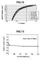
- FIG. 12 shows polarization curves obtained by the polarization measurement for an electrolytic plating bath of Example 1.
- FIG. 13 shows a graph obtained by plotting the current density at a potential of ⁇ 0.080 V, in the polarization curves at each rotating speeds shown in FIG. 12 .
- FIG. 14 shows polarization curves obtained by the polarization measurement for an electrolytic plating bath of Example 3.
- FIG. 15 shows a graph obtained by plotting the current density at a potential of ⁇ 0.035 V, in the polarization curves at each rotating speeds shown in FIG. 14 .
- FIG. 16 shows polarization curves obtained by the polarization measurement for an electrolytic plating bath of Example 5.
- FIG. 17 shows a graph obtained by plotting the current density at a potential of ⁇ 0.035 V, in the polarization curves at each rotating speeds shown in FIG. 16 .
- FIG. 18 is an illustration of the dimple on the upper side of the plating formed to fill a blind via-hole, measured in Comparative Examples 6 to 10 and Examples 7 to 12.
- FIG. 19 is an illustration of the thickness x of a plating film formed on a substrate surface and the thickness y of a plating film formed on the upper end of a side surface of a through-hole, measured in Comparative Examples 6 to 10 and Examples 7 to 12.
- An electrolytic copper plating bath contains a water-soluble copper salt, sulfuric acid, chloride ions, and a leveler as an additive, wherein the leveler is either one or both of a quaternary polyvinylimidazolium compound represented by the following formula (1) and a copolymer of vinylpyrrolidone and a quaternary vinylimidazolium compound, and the copolymer is represented by the following formula (2):
- R 1 and R 2 are each an alkyl group, preferably an alkyl group of 1 to 4 carbon atoms, more preferably methyl or ethyl, R 1 and R 2 may be the same or different, m is an integer of not less than 2, preferably an integer of 10 to 1000, and p and q are each an integer of not less than 1, preferably an integer of 10 to 1000.
- the nitrogen-containing compound called leveler functions as a cation in the acidic bath, and is electrically concentrated into electrically high-charged areas, thereby suppressing the deposition of the plating film.
- the effect of the nitrogen-containing compound can be expected whether it is a tertiary compound or a quaternary compound, but the quaternary compound bearing a positive charge is considered to have a stronger plating suppression.
- the quaternary polyvinylimidazolium compound contained in the electrolytic copper plating bath according to the present invention is a polymer of which the main chain is derived from the vinyl group, so that, unlike a monomer, its flexible straight chain moderates the influence of the steric hindrance, smoothly reaches the blind via-hole side surface, and the quaternary compound (cation) of imidazole of the rigid side chain is concentrated in high-charge areas, thereby giving a strong plating suppression as a leveler. Also, the copolymer of vinylpyrrolidone and the quaternary vinylimidazolium compound functions in the same manner.
- the diffusion rate of the leveler is higher than those of the levelers according to the conventional art.
- the diffusion rate is suitable for filling up not only the blind via-holes having a large diameter and a low aspect ratio, which have hitherto been the objects of filling up, but also the blind via-holes having a small diameter and a high aspect ratio, particularly a diameter of not less than 1 ⁇ m, preferably 1 to 100 ⁇ m, more preferably 5 to 50 ⁇ m, and an aspect ratio [(hole depth)/(hole diameter)] of not less than 2, preferably 2 to 10.
- the leveler is effectively supplied not only to the substrate surface side of blind via-holes (upper end portions of blind via-hole side surfaces) but also to central portions in the vertical direction of the blind via-hole side surfaces, so that the thickening of the plating film at the central portions of the blind via-holes is suppressed. Consequently the plating film grows preferentially from the bottom portions of the blind via-holes, and the blind via-holes can be filled up without generating cavities.
- the hole diameter and the aspect ratio of the blind via-holes of this substrate which has blind via-holes and through-holes
- the hole diameter is greater (not less than 50 ⁇ m) and the aspect ratio is lower (not more than 1), i.e., the blind via-holes are comparatively flat in shape, as compared with the blind via-holes of the above-mentioned substrate having only the blind via-holes. It becomes more difficult to fill up blind via-holes as the aspect ratio of the blind via-holes becomes higher.
- the plating solution according to the present invention is effective for filling up blind via-holes with a high aspect ratio, so that the plating solution naturally is effective for filling up the comparatively flat blind via-holes.
- the leveler is supplied to the whole part of the inside of each hole, so that even when through-hole plating is conducted simultaneously with the via-filling by an ordinary plating process, the plating film in the through-hole corner areas would not be thin, and an excellent plating film with a uniform film thickness can be formed in a comparatively short time.
- the diameter and the aspect ratio of the blind via-holes to be filled up are not particularly limited, but the plating bath according to the present invention is suitable for plating for a substrate having blind via-holes and through-holes, in which the blind via-holes have a diameter of not less than 1 ⁇ m, preferably 10 to 200 ⁇ m, more preferably 20 to 100 ⁇ m, and an aspect ratio [(hole depth)/(hole diameter)] of not less than 0.3, preferably 0.5 to 1.
- the shape of the blind via-holes which are objects to be treated in the present invention is not particularly limited.
- the aperture shape of the blind via-holes may be circle, ellipse, or polygon such as tetragon.
- the diameter is the length of the shortest one of the straight lines which pass through the center of gravity of the aperture plane and which connect arbitrary two points on the perimeter of the aperture.
- the present invention is suitable for filling up by plating for through electrodes 3 , 4 formed in a three-dimensionally mounted package in which a chip 2 is laminated on an interposer 1 formed of silicon or the like as shown in FIG. 2 , for example.
- symbol 5 donates a solder ball.
- the concentration of the leveler in the electrolytic copper plating bath according to the present invention is preferably 0.01 to 1000 mg/L, particularly 0.1 to 100 mg/L, more particularly 0.1 to 50 mg/L.
- the electrolytic copper plating bath contains a water-soluble copper salt, such as copper sulfate, as a source of copper; the concentration of the water-soluble copper salt, for example in the case of copper sulfate, is a concentration corresponding to 30 to 300 g/L as copper sulfate pentahydrate.
- the electrolytic copper plating bath according to the present invention contains sulfuric acid and chloride ions.
- the concentration of sulfuric acid is preferably 30 to 300 g/L, and the concentration of the chloride ions is preferably 5 to 150 mg/L, particularly 20 to 100 mg/L.
- chloride ion concentration exceeds 150 mg/L, copper chloride might be formed on the surface of the anode, leading to passivation of the anode.
- the chloride ion concentration is less than 5 mg/L, the plating suppression partially affects, and a stepped plating film is formed.
- the electrolytic copper plating bath according to the present invention to contain a brightener as a nucleation accelerator and/or a carrier as a nucleus growth suppressor, for achieving efficient deposition starting from the blind via-hole bottoms.
- the brightener preferably contains at least one selected from the group consisting of sulfur-containing additives represented by the following formulas (3) to (6):
- R 3 , R 4 and R 5 are each an alkyl group of 1 to 5 carbon atoms, preferably methyl or ethyl, R 3 , R 4 and R 5 may be the same or different, M is a hydrogen atom or an alkali metal such as sodium and potassium, a is an integer of 1 to 8, preferably 1 to 5, particularly preferably 3, and b, c and d are each 0 or 1.
- the brightener include those represented by the following formulas (8) to (11):
- the carrier preferably contains a polyalkylene glycol represented by the following formula (7): HO—(R 6 —O) e —H (7) where R 6 is an alkylene group of 2 or 3 carbon atoms (ethylene group or propylene group), the plurality of R 6 groups may be the same or different, and e is an integer of not less than 4, preferably 10 to 250.
- the alkylene glycol preferably has an average molecular weight (weight average molecular weight) of not less than 200, particularly 500 to 15000.
- the sulfur-containing compound used as the brightener has the function, by being accumulated in the inside of the blind via-holes, to accelerate the deposition of the plating metal starting from the bottom surfaces of the blind via-holes.
- the carrier has the function to increase polarization, by forming a complex with the Cu + ions and being adsorbed on the copper surface of the cathode, whereby uniform electro-deposition properties are enhanced.
- the complex interacts with the chloride ions, whereby the uniform electro-deposition properties are further enhanced.
- the carrier is preferably a polyalkylene glycol, for example, polyethylene glycol, polypropylene glycol, or an ethylene glycol-propylene glycol copolymer, that contains at least four alkylene groups.
- the plating film can be formed in a uniform film thickness, and the copper crystals constituting the plating film are made finer, leading to stabilization of the appearance of the plating.
- the ethylene glycol-propylene glycol copolymer is particularly preferred.
- the polyethylene glycol and polypropylene glycol tend to form reaction by-products when they are used for a long time, it may become difficult to conduct concentration control by CVS (Cyclic Voltammetry Stripping) which is a general analysis and control apparatus for plating bath additives including a water-soluble copper salt such as copper sulfate.
- CVS Cyclic Voltammetry Stripping
- the ethylene glycol-propylene glycol copolymer can be used for a long time without generating considerable influences of reaction by-products on the CVS; thus, the copolymer promises easy concentration control, is suited to long-time use, and is therefore preferable.
- the leveler When the leveler is used together with the brightener and the carrier, by the synergistic effect with the plating-suppression of the leveler on the area ranging from the substrate surface side of blind via-holes (blind via-hole side surface upper end portions) to the central portions in the vertical direction of the blind via-hole side surfaces, the plating film growth from the blind via-hole bottom side proceeds preferentially, whereby the blind via-holes can be securely filled up in a comparatively short time and without generating cavities. Furthermore, the dimple formed in an upper portion of the via-filling plating can be reduced, so that the plating film on the substrate surface (the surface to be plated) can be made thinner. Besides, plating at a high current density is made possible, and a shortening of the operation time can be expected.
- the concentration of the brightener in the electrolytic copper plating bath according to the present invention is preferably 0.1 to 100 mg/L, particularly 0.1 to 30 mg/L.
- the concentration of the carrier in the electrolytic copper plating bath of the present invention is desirably 0.05 to 2 g/L.
- a known plating process can be applied. Furthermore, a process can be applied in which the actions of a sulfur-containing compound (brightener) and a polyether compound (carrier), contained in a general electrolytic copper plating bath, are not provided in the electrolytic plating bath but given by a pretreatment with a pre-dipping solution, and thereafter electroplating is conducted in an electrolytic copper plating bath containing neither a brightener nor a carrier.
- blind via-holes formed on a substrate are filled up by plating with the above-described electrolytic copper plating bath.
- electroplating conditions conventionally known conditions can be applied. It is preferable to set the cathode current density in the range of 0.05 to 5 A/dm 2 , particularly 0.5 to 3 A/dm 2 .
- agitation can be effected by a generally used technique, for example, aeration, jet, squeegee or the like.
- the anode may be used any of known ones, including soluble anodes, such as steel plate, and insoluble anodes.
- the plating temperature can be 15 to 35° C., particularly 22 to 28° C.
- a silicon wafer was provided with blind via-holes having an aperture portion of 50 ⁇ m square, a depth of 150 ⁇ m and an aspect ratio of 3.0 by etching, and an insulation layer is formed on the inside walls of the blind via-holes. Thereafter, a Cu diffusion barrier layer (TiN) as a plating base coat layer and a seed layer (Cu) for the start of plating are formed on the wafer.
- TiN Cu diffusion barrier layer
- Cu seed layer
- an electrolytic copper plating bath containing 200 g/L of copper sulfate pentahydrate, 50 g/L of sulfuric acid, 50 mg/L of chloride ions, 2 mg/L of SPS [bis-(3-sodiumsulfopropyl) disulfide
- the blind via-hole was cut off, the section was polished to mirror surface, and the presence or absence of cavity was observed.
- the sectional shapes of the cavities were classified into three shapes shown in FIGS. 3A to 3C .
- cavity 1 is that classified into the shape shown in FIG. 3A
- cavity 2 is that classified into the shape shown in FIG. 3B
- cavity 3 is that classified into the shape shown in FIG. 3C .
- symbol 11 denotes a silicon wafer
- 12 denotes a blind via-hole
- 13 denotes copper (plating film)
- 14 denotes a cavity.
- the dimple formed in an upper portion of the blind via-hole was measured.
- the depth of the dimple is shown in FIG. 4 , in which symbol 11 denotes a silicon wafer, 12 denotes a blind via-hole, 13 denotes copper (plating film), and 15 denotes a dimple.
- symbol 11 denotes a silicon wafer
- 12 denotes a blind via-hole
- 13 denotes copper (plating film)
- 15 denotes a dimple.
- Via-filling plating was conducted in the same manner as in Comparative Example 1, except that 1-hydroxyethyl-2-alkylimidazoline chloride was used as the leveler, and the plating-filled state of the blind via-holes was evaluated. The results are given in Table 1.
- Via-filling plating was carried out in the same manner as in Comparative Example 1, except that a reaction product of benzyl chloride and polyethyleneimine was used as the leveler, and the plating-filled state of the blind via-holes was evaluated. The results are given in Table 1.
- a silicon wafer was provided with blind via-holes having an aperture portion of 50 ⁇ m square, a depth of 150 ⁇ m and an aspect ratio of 3.0 by etching, and an insulation layer was formed on the inside walls of the blind via-holes. Then, a Cu diffusion barrier layer (TiN) as a plating base coat layer and a seed layer (Cu) for the start of plating were formed on the wafer.
- TiN Cu diffusion barrier layer
- Cu seed layer
- an electrolytic copper plating bath containing 200 g/L of copper sulf
- a silicon wafer was provided with blind via-holes having an aperture portion of 50 ⁇ m square, a depth of 150 ⁇ m and an aspect ratio of 3.0 by etching, and an insulation layer was formed on the inside walls of the blind via-holes. Thereafter, a Cu diffusion barrier layer (TiN) as a plating base coat layer and a seed layer (Cu) for the start of plating were formed on the wafer.
- TiN Cu diffusion barrier layer
- Cu seed layer
- an electrolytic copper plating bath containing 50 g/L
- a silicon wafer was provided with blind via-holes having an aperture portion of 50 ⁇ m square, a depth of 150 ⁇ m and an aspect ratio of 3.0 by etching, and an insulation layer is formed on the inside walls of the blind via-holes. Thereafter, a Cu diffusion barrier layer (TiN) as a plating base coat layer and a seed layer (Cu) for the start of plating were formed on the wafer.
- TiN Cu diffusion barrier layer
- Cu seed layer
- an electrolytic copper plating bath containing 250 g/L of copper sulfate pentahydrate, 40 g/L of sulfur
- a silicon wafer was provided with blind via-holes having an aperture portion of 50 ⁇ m square, a depth of 150 ⁇ m and an aspect ratio of 3.0 by etching, and an insulation layer was formed on the inside walls of the blind via-holes. Thereafter, a Cu diffusion barrier layer (TiN) as a plating base coat layer and a seed layer (Cu) for the start of plating were formed on the wafer.
- TiN Cu diffusion barrier layer
- Cu seed layer
- an electrolytic copper plating bath containing 100 g/L of copper sulfate pentahydrate, 250 g/L of sulfuric acid, 20 mg/L of chlor
- a silicon wafer was provided with blind via-holes having an aperture portion of 50 ⁇ m square, a depth of 150 ⁇ m and an aspect ratio of 3.0 by etching, and an insulation layer was formed on the inside walls of the blind via-holes. Thereafter, a Cu diffusion barrier layer (TiN) as a plating base coat layer and a seed layer (Cu) for the start of plating were formed on the wafer.
- TiN Cu diffusion barrier layer
- Cu seed layer
- an electrolytic copper plating bath containing 200 g
- a silicon wafer was provided with blind via-holes having an aperture portion of 50 ⁇ m square, a depth of 150 ⁇ m and an aspect ratio of 3.0 by etching, and an insulation layer was formed on the inside walls of the blind via-holes. Thereafter, a Cu diffusion barrier layer (TiN) as a plating base coat layer and a seed layer (Cu) for the start of plating were formed on the wafer.
- TiN Cu diffusion barrier layer
- Cu seed layer
- the plating solutions used in Comparative Example 1, Comparative Example 4, Comparative Example 3, Example 1, Example 3 and Example 5 were evaluated their electrochemical characteristics by cathode polarization measurement using a rotating electrode.
- an electrode is rotated at a fixed speed to generate a liquid flow, whereby mass transfer according to the rotating speed is induced on the electrode surface, and the mass transfer rates in the inside and the outside of blind via-hole were measured in a simulated manner.
- Comparative Example 1 the relationship between the current densities at the different rotating speeds is in the manner of 50 rpm ⁇ 500 rpm>1000 rpm; thus, the difference in current density is large in a high rotating speed region, and is small in medium and low rotating speed regions. This means that since the diffusion rate of the leveler is too low, the plating-suppression is effective in the high rotating speed region (the diffusion layer is thin) but is not so effective in the medium to low rotating speed regions (the diffusion layer is medium to thick).
- the supply of the leveler is insufficient in the area ranging from an upper portion to an intermediate portion of the blind via-hole wall surface where the diffusion layer is not so thick, and the deposition in the area ranging from the upper portion to the intermediate portion of the blind via-hole wall surface cannot be suppressed.
- the supply of the leveler is little at the blind via-hole bottom portion, however, since the potential at the blind via-hole bottom is lower than that in the area ranging from the upper portion to the intermediate portion of the blind via-hole wall surface, plating from the bottom portion does not take place, and a large cavity as shown in FIG. 3A [Cavity 1 ] is generated.
- the relationship between the current densities at the different rotating speeds is in the manner of 50 rpm>500 rpm>1000 rpm; thus, the current density decreases linearly as the rotating speed is raised.
- the diffusion rate of the leveler in this case is slightly higher than that in Comparative Example 1, and the plating-suppression is effective also in the medium rotating speed region (the diffusion layer has a medium thickness).
- the difference in current density between the high rotating speed region and the medium rotating speed region is large, so that the diffusion rate of the leveler is not yet enough to fill up the high-aspect-ratio blind via-holes (the difference in diffusion layer thickness is large) without generation cavities (seams).
- the plating-suppression is uniformly at the blind via-hole wall surface and the blind via-hole bottom portion, and the plating film is deposited along the shape of the blind via-hole, so that in the blind via-hole with a high aspect ratio, a cavity (seam) is generated at the blind via-hole central portion as shown in FIG. 3C [Cavity 3 ].
- the current densities at the different rotating speeds are in the relationship of 50 rpm>500 rpm ⁇ 1000 rpm; thus, the difference in current density between 500 and 1000 rpm is smaller than those in Comparative Example 1 and Comparative Example 4, and the current density at 50 rpm is somewhat higher than those at 500 rpm and 1000 rpm, unlike in Comparative Example 3.
- the diffusion rate of the leveler is higher than those in Comparative Example 1 and Comparative Example 4, and is lower than that in Comparative Example 3.
- the leveler with such a diffusion rate shows a somewhat high diffusion rate even in the area ranging from an upper portion to an intermediate portion of the blind via-hole wall surface where the diffusion layer is somewhat thick, so that the leveler can be supplied to the area, and deposition in the area can be suppressed.
- the supply of the leveler is insufficient at the blind via-hole bottom portion where the diffusion layer is thicker than in the area ranging from the upper portion to the intermediate portion of the blind via-hole wall surface, so that the plating-suppression is weak and the plating film grows at a sufficient rate at the blind via-hole bottom portion.
- the leveler having such a diffusion rate is a leveler suited to filling up blind via-holes having a high aspect ratio.
- a substrate provided with both blind via-holes having an aperture of 70 ⁇ m ⁇ , a depth of 45 ⁇ m (copper layer portion 10 ⁇ m+resin layer portion 35 ⁇ m) and an aspect ratio of 0.64 and through-holes penetrating through the substrate in the thickness direction and having an aperture of 0.3 mm ⁇ and a length of 0.6 mm was subjected to a desmear treatment, giving of a catalyst and a chemical copper plating (film thickness: about 0.5 ⁇ m) treatment by known methods.
- the blind via-hole was cut off, the section was polished to mirror surface, and the dimple in an upper portion of the plating film having filled up the blind via-hole was measured.
- the depth of the dimple is shown in FIG. 18 , in which symbol 101 denotes a resin layer, 102 denotes a blind via-hole, 103 denotes a copper layer, 104 denotes copper (plating film), and 105 denotes a dimple.
- symbol 101 denotes a resin layer
- 102 denotes a blind via-hole
- 103 denotes a copper layer
- 104 denotes copper (plating film)
- 105 denotes a dimple.
- a vertical section passing through the center of the aperture of the through-hole was cut off, the vertical section was polished to mirror surface, then the thickness x of the plating film formed on the substrate surface shown in FIG. 19 and the thickness (the thickness at a position of 135° relative to a through-hole side surface) y of the plating film formed at the through-hole side surface upper end (the substrate corner in the vertical section) were measured, and their ratio (y/x) was calculated.
- the results are also shown in Table 3.
- symbol 111 denotes a resin layer
- 112 denotes a copper layer
- 113 denotes copper (plating film)
- 116 denotes a through-hole.
- a substrate provided with both blind via-holes having an aperture of 70 ⁇ m ⁇ , a depth of 45 ⁇ m (copper layer portion 10 ⁇ m+resin layer portion 35 ⁇ m) and an aspect ratio of 0.64 and through-holes penetrating through the substrate in the thickness direction and having an aperture of 0.3 mm ⁇ and a length of 0.6 mm was subjected to a desmear treatment, giving of a catalyst, and a chemical copper plating (film thickness: about 0.5 ⁇ m) treatment by known methods.
- a substrate provided with both blind via-holes having an aperture of 70 ⁇ m ⁇ , a depth of 45 ⁇ m (copper layer portion 10 ⁇ m+resin layer portion 35 ⁇ m) and an aspect ratio of 0.64 and through-holes penetrating through the substrate in the thickness direction and having an aperture of 0.3 mm ⁇ and a length of 0.6 mm was subjected to a desmear treatment, giving of a catalyst and a chemical copper plating (film thickness: about 0.5 ⁇ m) treatment by known methods.
- a substrate provided with both blind via-holes having an aperture of 70 ⁇ m ⁇ , a depth of 45 ⁇ m (copper layer portion 10 ⁇ m+resin layer portion 35 ⁇ m) and an aspect ratio of 0.64 and through-holes penetrating through the substrate in the thickness direction and having an aperture of 0.3 mm ⁇ and a length of 0.6 mm was subjected to a desmear treatment, giving of a catalyst and a chemical copper plating (film thickness: about 0.5 ⁇ m) treatment by known methods.
- a substrate provided with both blind via-holes having an aperture of 70 ⁇ m ⁇ , a depth of 45 ⁇ m (copper layer portion 10 ⁇ m+resin layer portion 35 ⁇ m) and an aspect ratio of 0.64 and through-holes penetrating through the substrate in the thickness direction and having an aperture of 0.3 mm ⁇ and a length of 0.6 mm was subjected to a desmear treatment, giving of a catalyst and a chemical copper plating (film thickness: about 0.5 ⁇ m) treatment by known methods.
- a substrate provided with both blind via-holes having an aperture of 70 ⁇ m ⁇ , a depth of 45 ⁇ m (copper layer portion 10 ⁇ m+resin layer portion 35 ⁇ m) and an aspect ratio of 0.64 and through-holes penetrating through the substrate in the thickness direction and having an aperture of 0.3 mm ⁇ and a length of 0.6 mm was subjected to a desmear treatment, giving of a catalyst and a chemical copper plating (film thickness: about 0.5 ⁇ m) treatment by known methods.
- a substrate provided with both blind via-holes having an aperture of 70 ⁇ m ⁇ , a depth of 45 ⁇ m (copper layer portion 10 ⁇ m+resin layer portion 35 ⁇ m) and an aspect ratio of 0.64 and through-holes penetrating through the substrate in the thickness direction and having an aperture of 0.3 mm ⁇ and a length of 0.6 mm was subjected to a desmear treatment, giving of a catalyst and a chemical copper plating (film thickness: about 0.5 ⁇ m) treatment by known methods.
- a substrate provided with both blind via-holes having an aperture of 70 ⁇ m ⁇ , a depth of 45 ⁇ m (copper layer portion 10 ⁇ m+resin layer portion 35 ⁇ m) and an aspect ratio of 0.64 and through-holes penetrating through the substrate in the thickness direction and having an aperture of 0.3 mm ⁇ and a length of 0.6 mm was subjected to a desmear treatment, giving of a catalyst and a chemical copper plating (film thickness: about 0.5 ⁇ m) treatment by known methods.
- a substrate provided with both blind via-holes having an aperture of 70 ⁇ m ⁇ , a depth of 45 ⁇ m (copper layer portion 10 ⁇ m+resin layer portion 35 ⁇ m) and an aspect ratio of 0.64 and through-holes penetrating through the substrate in the thickness direction and having an aperture of 0.3 mm ⁇ and a length of 0.6 mm was subjected to a desmear treatment, giving of a catalyst and a chemical copper plating (film thickness: about 0.5 ⁇ m) treatment by known methods.
- a substrate provided with both blind via-holes having an aperture of 70 ⁇ m ⁇ , a depth of 45 ⁇ m (copper layer portion 10 ⁇ m+resin layer portion 35 ⁇ m) and an aspect ratio of 0.64 and through-holes penetrating through the substrate in the thickness direction and having an aperture of 0.3 mm ⁇ and a length of 0.6 mm was subjected to a desmear treatment, giving of a catalyst and a chemical copper plating (film thickness: about 0.5 ⁇ m) treatment by known methods.
- a substrate provided with both blind via-holes having an aperture of 70 ⁇ m ⁇ , a depth of 45 ⁇ m (copper layer portion 10 ⁇ m+resin layer portion 35 ⁇ m) and an aspect ratio of 0.64 and through-holes penetrating through the substrate in the thickness direction and having an aperture of 0.3 mm ⁇ and a length of 0.6 mm was subjected to a desmear treatment, giving of a catalyst and a chemical copper plating (film thickness: about 0.5 ⁇ m) treatment by known methods.
- the plating of blind via-holes could be achieved without generating any cavity in all the comparative examples and the examples; however, in Comparative Example 8, the dimple was large, and the blind via-hole was not filled up but plated with plating metal along the shape of the blind via-hole.
- the plating film at the through-hole side surface upper end was thick in Comparative Examples 6, 7, 9 and 10, and even the maximum thereof was as insufficient as not more than 50% based on the plating film thickness on the substrate surface.
- the blind via-holes could be filled up in the condition where the dimple is sufficiently small, the values of the plating film thickness at the through-hole side surface upper end (the substrate corner portion in the vertical section shown in FIG. 19 ) were at least 68% based on the plating film thickness on the substrate surface, and the plating film was formed substantially along the substrate shape.
Applications Claiming Priority (4)
| Application Number | Priority Date | Filing Date | Title |
|---|---|---|---|
| JP2004-215561 | 2004-07-23 | ||
| JP2004215561 | 2004-07-23 | ||
| JP2005-201080 | 2005-07-11 | ||
| JP2005201080A JP4973829B2 (ja) | 2004-07-23 | 2005-07-11 | 電気銅めっき浴及び電気銅めっき方法 |
Publications (2)
| Publication Number | Publication Date |
|---|---|
| US20060207886A1 US20060207886A1 (en) | 2006-09-21 |
| US7220347B2 true US7220347B2 (en) | 2007-05-22 |
Family
ID=36104896
Family Applications (1)
| Application Number | Title | Priority Date | Filing Date |
|---|---|---|---|
| US11/181,856 Active 2025-07-18 US7220347B2 (en) | 2004-07-23 | 2005-07-15 | Electrolytic copper plating bath and plating process therewith |
Country Status (5)
| Country | Link |
|---|---|
| US (1) | US7220347B2 (zh) |
| JP (1) | JP4973829B2 (zh) |
| KR (1) | KR101165222B1 (zh) |
| CN (1) | CN100595343C (zh) |
| TW (1) | TWI365924B (zh) |
Cited By (15)
| Publication number | Priority date | Publication date | Assignee | Title |
|---|---|---|---|---|
| US20090057156A1 (en) * | 2007-08-30 | 2009-03-05 | Hitachi Cable, Ltd. | Production method for wiring and vias |
| US20090236230A1 (en) * | 2004-09-20 | 2009-09-24 | Bert Reents | Galvanic process for filling through-holes with metals, in particular of printed circuit boards with copper |
| US20090301889A1 (en) * | 2006-03-30 | 2009-12-10 | Atotech Deutschland Gmbh | Electrolytic Method For Filling Holes and Cavities With Metals |
| US20100003399A1 (en) * | 2008-07-01 | 2010-01-07 | C. Uyemura & Co., Ltd. | Electroless plating solution, method for electroless plating using the same and method for manufacturing circuit board |
| US20100084277A1 (en) * | 2008-10-06 | 2010-04-08 | Myung-Beom Park | Composition for copper plating and associated methods |
| US20100219081A1 (en) * | 2007-05-21 | 2010-09-02 | C. Uyemura & Co., Ltd. | Copper electroplating bath |
| US20110062029A1 (en) * | 2009-09-16 | 2011-03-17 | C. Uyemura & Co., Ltd. | Electrolytic copper plating bath and method for electroplating using the electrolytic copper plating bath |
| US20110108427A1 (en) * | 2008-09-30 | 2011-05-12 | Charan Gurumurthy | Substrate package with through holes for high speed i/o flex cable |
| US20110171491A1 (en) * | 2008-07-07 | 2011-07-14 | Furukawa Electric Co., Ltd. | Electrodeposited copper foil and copper clad laminate |
| WO2012014029A1 (en) | 2010-07-29 | 2012-02-02 | Atotech Deutschland Gmbh | Process for electrodeposition of copper chip to chip, chip to wafer and wafer to wafer interconnects in through-silicon vias (tsv) with heated substrate and cooled electrolyte |
| US20120189811A1 (en) * | 2007-03-15 | 2012-07-26 | Nippon Mining & Metals Co., Ltd. | Copper electrolytic solution and two-layer flexible substrate obtained using the same |
| US20120211369A1 (en) * | 2011-02-18 | 2012-08-23 | Myung-Beom Park | Copper electroplating method |
| US9637833B2 (en) | 2011-12-22 | 2017-05-02 | Rohm And Haas Electronic Materials Llc | Copper electroplating solution and method of copper electroplating |
| US10917966B2 (en) | 2018-01-29 | 2021-02-09 | Corning Incorporated | Articles including metallized vias |
| US10932371B2 (en) | 2014-11-05 | 2021-02-23 | Corning Incorporated | Bottom-up electrolytic via plating method |
Families Citing this family (35)
| Publication number | Priority date | Publication date | Assignee | Title |
|---|---|---|---|---|
| JP4976725B2 (ja) * | 2005-03-31 | 2012-07-18 | 三井金属鉱業株式会社 | 銅電解液及びその銅電解液を用いた電析銅皮膜の形成方法 |
| JP4816901B2 (ja) * | 2005-11-21 | 2011-11-16 | 上村工業株式会社 | 電気銅めっき浴 |
| JP4895734B2 (ja) * | 2006-09-08 | 2012-03-14 | 荏原ユージライト株式会社 | めっき用レベリング剤、酸性銅めっき浴用添加剤組成物、酸性銅めっき浴および該めっき浴を用いるめっき方法 |
| US7887693B2 (en) * | 2007-06-22 | 2011-02-15 | Maria Nikolova | Acid copper electroplating bath composition |
| US20090038947A1 (en) * | 2007-08-07 | 2009-02-12 | Emat Technology, Llc. | Electroplating aqueous solution and method of making and using same |
| JP2010018885A (ja) * | 2008-06-12 | 2010-01-28 | Furukawa Electric Co Ltd:The | 電解銅皮膜、その製造方法及び銅電解皮膜製造用の銅電解液 |
| US20100059385A1 (en) * | 2008-09-06 | 2010-03-11 | Delin Li | Methods for fabricating thin film solar cells |
| US8388824B2 (en) * | 2008-11-26 | 2013-03-05 | Enthone Inc. | Method and composition for electrodeposition of copper in microelectronics with dipyridyl-based levelers |
| JP2010255078A (ja) * | 2009-04-28 | 2010-11-11 | Adeka Corp | 電解銅めっき浴および電解銅めっき方法 |
| JP4699565B2 (ja) * | 2009-05-29 | 2011-06-15 | 三井化学株式会社 | 半導体用シール組成物、半導体装置および半導体装置の製造方法 |
| US9677188B2 (en) | 2009-06-17 | 2017-06-13 | Novellus Systems, Inc. | Electrofill vacuum plating cell |
| TWI487815B (zh) * | 2010-01-27 | 2015-06-11 | Ebara Corp | 鍍覆方法與鍍覆裝置 |
| WO2011135673A1 (ja) * | 2010-04-27 | 2011-11-03 | 荏原ユージライト株式会社 | 新規化合物およびその用途 |
| TWI523976B (zh) * | 2010-05-19 | 2016-03-01 | 諾菲勒斯系統公司 | 利用具有雙態抑制劑的電解液之矽穿孔填充 |
| KR101829866B1 (ko) | 2010-06-01 | 2018-02-20 | 바스프 에스이 | 레벨링제를 포함하는 금속 전기도금용 조성물 |
| EP2392692A1 (en) | 2010-06-01 | 2011-12-07 | Basf Se | Composition for metal electroplating comprising leveling agent |
| US20120097547A1 (en) * | 2010-10-25 | 2012-04-26 | Universiteit Gent | Method for Copper Electrodeposition |
| KR20120088124A (ko) * | 2011-01-31 | 2012-08-08 | 삼성전자주식회사 | 구리 도금용 조성물 및 이를 이용한 구리 범프 형성 방법 |
| JP5762137B2 (ja) | 2011-05-27 | 2015-08-12 | 上村工業株式会社 | めっき方法 |
| JP5952093B2 (ja) * | 2012-05-31 | 2016-07-13 | ローム・アンド・ハース電子材料株式会社 | 電解銅めっき液及び電解銅めっき方法 |
| CN103060860B (zh) * | 2013-01-22 | 2016-01-20 | 中南大学 | 一种印制线路板酸性镀铜电镀液及其制备和应用方法 |
| US9613833B2 (en) | 2013-02-20 | 2017-04-04 | Novellus Systems, Inc. | Methods and apparatus for wetting pretreatment for through resist metal plating |
| US9677190B2 (en) * | 2013-11-01 | 2017-06-13 | Lam Research Corporation | Membrane design for reducing defects in electroplating systems |
| US9435049B2 (en) | 2013-11-20 | 2016-09-06 | Lam Research Corporation | Alkaline pretreatment for electroplating |
| CN103572335B (zh) * | 2013-11-20 | 2016-04-13 | 东莞市富默克化工有限公司 | 一种pcb通孔电镀铜溶液及其制备方法和电镀方法 |
| CN104532308B (zh) * | 2014-12-31 | 2017-03-08 | 上海新阳半导体材料股份有限公司 | 一种用于酸性电镀铜的整平剂及其用途 |
| US9617648B2 (en) | 2015-03-04 | 2017-04-11 | Lam Research Corporation | Pretreatment of nickel and cobalt liners for electrodeposition of copper into through silicon vias |
| CN104694982B (zh) * | 2015-03-05 | 2018-04-27 | 中国科学院过程工程研究所 | 一种含有离子液体添加剂的无氰电镀黄铜镀液及其使用方法 |
| KR101657675B1 (ko) * | 2015-09-25 | 2016-09-22 | 한국생산기술연구원 | 2종의 평탄제를 포함하는 전해 구리 도금용 유기첨가제 및 이를 포함하는 전해 구리 도금액 |
| KR101733141B1 (ko) * | 2016-03-18 | 2017-05-08 | 한국생산기술연구원 | 고평탄 구리도금막 형성을 위한 전해 구리 도금용 유기첨가제 및 이를 포함하는 전해구리 도금액 |
| JP6948053B2 (ja) | 2017-01-12 | 2021-10-13 | 上村工業株式会社 | フィリングめっきシステム及びフィリングめっき方法 |
| KR102445636B1 (ko) | 2017-11-28 | 2022-09-22 | 솔브레인 주식회사 | 평탄화제 및 이를 포함하는 구리 도금 조성물 |
| US11871514B2 (en) | 2020-04-01 | 2024-01-09 | Sumitomo Electric Industries, Ltd. | Flexible printed circuit board and method for producing the same |
| CN113278104A (zh) * | 2021-05-10 | 2021-08-20 | 江苏理工学院 | 一种季铵盐表面活性剂及其制备方法 |
| CN117684223A (zh) * | 2022-09-02 | 2024-03-12 | 宁波安集微电子科技有限公司 | 一种金属电镀组合物及其使用方法 |
Citations (2)
| Publication number | Priority date | Publication date | Assignee | Title |
|---|---|---|---|---|
| US3502551A (en) * | 1966-08-20 | 1970-03-24 | Schering Ag | Acid electrolyte for the deposition of bright,levelling copper coatings |
| US20050016858A1 (en) * | 2002-12-20 | 2005-01-27 | Shipley Company, L.L.C. | Reverse pulse plating composition and method |
Family Cites Families (10)
| Publication number | Priority date | Publication date | Assignee | Title |
|---|---|---|---|---|
| JPS57114685A (en) * | 1981-01-07 | 1982-07-16 | Kuraray Co Ltd | Brightener for plating bath |
| CN1181530C (zh) * | 1996-12-16 | 2004-12-22 | 国际商业机器公司 | 集成电路芯片上的电镀互连结构 |
| EP1153430B1 (de) * | 1999-01-21 | 2004-11-10 | ATOTECH Deutschland GmbH | Verfahren zum galvanischen bilden von leiterstrukturen aus hochreinem kupfer bei der herstellung von integrierten schaltungen |
| KR100366631B1 (ko) * | 2000-09-27 | 2003-01-09 | 삼성전자 주식회사 | 폴리비닐피롤리돈을 포함하는 구리도금 전해액 및 이를이용한 반도체 소자의 구리배선용 전기도금방법 |
| JP3780302B2 (ja) * | 2002-02-27 | 2006-05-31 | 株式会社関東学院大学表面工学研究所 | ビアホール及びスルーホールを有する基板のめっき方法 |
| US7316772B2 (en) * | 2002-03-05 | 2008-01-08 | Enthone Inc. | Defect reduction in electrodeposited copper for semiconductor applications |
| JP2003328179A (ja) * | 2002-05-10 | 2003-11-19 | Ebara Udylite Kk | 酸性銅めっき浴用添加剤及び該添加剤を含有する酸性銅めっき浴並びに該めっき浴を用いるめっき方法 |
| KR20040003216A (ko) | 2002-07-02 | 2004-01-13 | 기아자동차주식회사 | 차량의 전방필러에 의한 운전사각 모니터장치 |
| JP4031328B2 (ja) * | 2002-09-19 | 2008-01-09 | 荏原ユージライト株式会社 | 酸性銅めっき浴用添加剤及び該添加剤を含有する酸性銅めっき浴並びに該めっき浴を用いるめっき方法 |
| EP1422320A1 (en) * | 2002-11-21 | 2004-05-26 | Shipley Company, L.L.C. | Copper electroplating bath |
-
2005
- 2005-07-11 JP JP2005201080A patent/JP4973829B2/ja active Active
- 2005-07-14 TW TW094123951A patent/TWI365924B/zh active
- 2005-07-15 US US11/181,856 patent/US7220347B2/en active Active
- 2005-07-20 KR KR1020050065840A patent/KR101165222B1/ko active IP Right Grant
- 2005-07-22 CN CN200510106721A patent/CN100595343C/zh active Active
Patent Citations (2)
| Publication number | Priority date | Publication date | Assignee | Title |
|---|---|---|---|---|
| US3502551A (en) * | 1966-08-20 | 1970-03-24 | Schering Ag | Acid electrolyte for the deposition of bright,levelling copper coatings |
| US20050016858A1 (en) * | 2002-12-20 | 2005-01-27 | Shipley Company, L.L.C. | Reverse pulse plating composition and method |
Cited By (26)
| Publication number | Priority date | Publication date | Assignee | Title |
|---|---|---|---|---|
| US20090236230A1 (en) * | 2004-09-20 | 2009-09-24 | Bert Reents | Galvanic process for filling through-holes with metals, in particular of printed circuit boards with copper |
| US9526183B2 (en) | 2004-09-20 | 2016-12-20 | Atotech Deutschland Gmbh | Galvanic process for filling through-holes with metals, in particular of printed circuit boards with copper |
| US9445510B2 (en) * | 2004-09-20 | 2016-09-13 | Atotech Deutschland Gmbh | Galvanic process for filling through-holes with metals, in particular of printed circuit boards with copper |
| US8784634B2 (en) * | 2006-03-30 | 2014-07-22 | Atotech Deutschland Gmbh | Electrolytic method for filling holes and cavities with metals |
| US20090301889A1 (en) * | 2006-03-30 | 2009-12-10 | Atotech Deutschland Gmbh | Electrolytic Method For Filling Holes and Cavities With Metals |
| US20120189811A1 (en) * | 2007-03-15 | 2012-07-26 | Nippon Mining & Metals Co., Ltd. | Copper electrolytic solution and two-layer flexible substrate obtained using the same |
| US8679317B2 (en) * | 2007-05-21 | 2014-03-25 | C. Uyemura & Co., Ltd. | Copper electroplating bath |
| US20100219081A1 (en) * | 2007-05-21 | 2010-09-02 | C. Uyemura & Co., Ltd. | Copper electroplating bath |
| US20090057156A1 (en) * | 2007-08-30 | 2009-03-05 | Hitachi Cable, Ltd. | Production method for wiring and vias |
| US20100003399A1 (en) * | 2008-07-01 | 2010-01-07 | C. Uyemura & Co., Ltd. | Electroless plating solution, method for electroless plating using the same and method for manufacturing circuit board |
| US20120058254A1 (en) * | 2008-07-01 | 2012-03-08 | C. Uyemura & Co., Ltd. | Electroless plating solution, method for electroless plating using the same and method for manufacturing circuit board |
| US8137447B2 (en) * | 2008-07-01 | 2012-03-20 | C. Uyemura & Co., Ltd. | Electroless plating solution, method for electroless plating using the same and method for manufacturing circuit board |
| US8197583B2 (en) * | 2008-07-01 | 2012-06-12 | C. Uyemura & Co., Ltd. | Electroless plating solution, method for electroless plating using the same and method for manufacturing circuit board |
| US20110171491A1 (en) * | 2008-07-07 | 2011-07-14 | Furukawa Electric Co., Ltd. | Electrodeposited copper foil and copper clad laminate |
| US20110108427A1 (en) * | 2008-09-30 | 2011-05-12 | Charan Gurumurthy | Substrate package with through holes for high speed i/o flex cable |
| US8353101B2 (en) * | 2008-09-30 | 2013-01-15 | Intel Corporation | Method of making substrate package with through holes for high speed I/O flex cable |
| US20100084277A1 (en) * | 2008-10-06 | 2010-04-08 | Myung-Beom Park | Composition for copper plating and associated methods |
| US20110062029A1 (en) * | 2009-09-16 | 2011-03-17 | C. Uyemura & Co., Ltd. | Electrolytic copper plating bath and method for electroplating using the electrolytic copper plating bath |
| US9028668B2 (en) * | 2009-09-16 | 2015-05-12 | C. Uyemura & Co., Ltd | Electrolytic copper plating bath and method for electroplating using the electrolytic copper plating bath |
| KR101737501B1 (ko) | 2009-09-16 | 2017-05-18 | 우에무라 고교 가부시키가이샤 | 전기 구리 도금욕 및 이 전기 구리 도금욕을 사용한 전기 도금 방법 |
| WO2012014029A1 (en) | 2010-07-29 | 2012-02-02 | Atotech Deutschland Gmbh | Process for electrodeposition of copper chip to chip, chip to wafer and wafer to wafer interconnects in through-silicon vias (tsv) with heated substrate and cooled electrolyte |
| US8795505B2 (en) * | 2011-02-18 | 2014-08-05 | Samsung Electronics Co., Ltd. | Copper electroplating method |
| US20120211369A1 (en) * | 2011-02-18 | 2012-08-23 | Myung-Beom Park | Copper electroplating method |
| US9637833B2 (en) | 2011-12-22 | 2017-05-02 | Rohm And Haas Electronic Materials Llc | Copper electroplating solution and method of copper electroplating |
| US10932371B2 (en) | 2014-11-05 | 2021-02-23 | Corning Incorporated | Bottom-up electrolytic via plating method |
| US10917966B2 (en) | 2018-01-29 | 2021-02-09 | Corning Incorporated | Articles including metallized vias |
Also Published As
| Publication number | Publication date |
|---|---|
| CN1900377A (zh) | 2007-01-24 |
| JP4973829B2 (ja) | 2012-07-11 |
| US20060207886A1 (en) | 2006-09-21 |
| CN100595343C (zh) | 2010-03-24 |
| TW200607887A (en) | 2006-03-01 |
| KR20060053951A (ko) | 2006-05-22 |
| JP2006057177A (ja) | 2006-03-02 |
| TWI365924B (en) | 2012-06-11 |
| KR101165222B1 (ko) | 2012-07-17 |
Similar Documents
| Publication | Publication Date | Title |
|---|---|---|
| US7220347B2 (en) | Electrolytic copper plating bath and plating process therewith | |
| US6444110B2 (en) | Electrolytic copper plating method | |
| JP4816901B2 (ja) | 電気銅めっき浴 | |
| US6776893B1 (en) | Electroplating chemistry for the CU filling of submicron features of VLSI/ULSI interconnect | |
| US6610192B1 (en) | Copper electroplating | |
| JP6111241B2 (ja) | 銅の電解析出用水性酸浴、当該浴の使用、当該浴中のルテニウムイオンの使用、および、当該浴を用いた加工対象物上への銅の電解析出方法 | |
| KR101417986B1 (ko) | 전기 구리 도금욕 | |
| US20040045832A1 (en) | Electrolytic copper plating solutions | |
| US20110089044A1 (en) | Copper electrolytic plating bath and copper electrolytic plating method | |
| US20020127847A1 (en) | Electrochemical co-deposition of metals for electronic device manufacture | |
| EP1422320A1 (en) | Copper electroplating bath | |
| US20060183328A1 (en) | Electrolytic copper plating solutions | |
| US8273232B2 (en) | Copper filling-up method | |
| US20080087549A1 (en) | Additive For Copper Plating And Process For Producing Electronic Circiut Substrate Therewith | |
| US20040222104A1 (en) | Electroplating composition | |
| US10435380B2 (en) | Metal plating compositions | |
| KR102125240B1 (ko) | 아민과 폴리아크릴아미드와 설톤의 반응 생성물의 화합물을 함유하는 구리 전기도금욕 | |
| JP4154571B2 (ja) | 硫酸銅めっき浴及び電気銅めっき方法 | |
| TW202146708A (zh) | 用於電解沉積銅沉積物之酸性水性組合物 |
Legal Events
| Date | Code | Title | Description |
|---|---|---|---|
| AS | Assignment |
Owner name: C. UYEMURA & CO., LTD., JAPAN Free format text: ASSIGNMENT OF ASSIGNORS INTEREST;ASSIGNORS:ISONO, TOSHIHISA;TACHIBANA, SHINJI;KAWASE, TOMOHIRO;AND OTHERS;REEL/FRAME:017139/0743 Effective date: 20050728 |
|
| STCF | Information on status: patent grant |
Free format text: PATENTED CASE |
|
| FPAY | Fee payment |
Year of fee payment: 4 |
|
| FPAY | Fee payment |
Year of fee payment: 8 |
|
| MAFP | Maintenance fee payment |
Free format text: PAYMENT OF MAINTENANCE FEE, 12TH YEAR, LARGE ENTITY (ORIGINAL EVENT CODE: M1553); ENTITY STATUS OF PATENT OWNER: LARGE ENTITY Year of fee payment: 12 |