US7212713B2 - Optical transmission substrate, method for manufacturing optical transmission substrate and optoelectronic integrated circuit - Google Patents
Optical transmission substrate, method for manufacturing optical transmission substrate and optoelectronic integrated circuit Download PDFInfo
- Publication number
- US7212713B2 US7212713B2 US10/977,170 US97717004A US7212713B2 US 7212713 B2 US7212713 B2 US 7212713B2 US 97717004 A US97717004 A US 97717004A US 7212713 B2 US7212713 B2 US 7212713B2
- Authority
- US
- United States
- Prior art keywords
- substrate
- optical
- core
- light
- optical waveguide
- Prior art date
- Legal status (The legal status is an assumption and is not a legal conclusion. Google has not performed a legal analysis and makes no representation as to the accuracy of the status listed.)
- Active, expires
Links
Images


Classifications
-
- G—PHYSICS
- G02—OPTICS
- G02B—OPTICAL ELEMENTS, SYSTEMS OR APPARATUS
- G02B6/00—Light guides; Structural details of arrangements comprising light guides and other optical elements, e.g. couplings
- G02B6/24—Coupling light guides
- G02B6/26—Optical coupling means
- G02B6/30—Optical coupling means for use between fibre and thin-film device
-
- G—PHYSICS
- G02—OPTICS
- G02B—OPTICAL ELEMENTS, SYSTEMS OR APPARATUS
- G02B6/00—Light guides; Structural details of arrangements comprising light guides and other optical elements, e.g. couplings
- G02B6/10—Light guides; Structural details of arrangements comprising light guides and other optical elements, e.g. couplings of the optical waveguide type
- G02B6/12—Light guides; Structural details of arrangements comprising light guides and other optical elements, e.g. couplings of the optical waveguide type of the integrated circuit kind
- G02B6/122—Basic optical elements, e.g. light-guiding paths
- G02B6/125—Bends, branchings or intersections
-
- G—PHYSICS
- G02—OPTICS
- G02B—OPTICAL ELEMENTS, SYSTEMS OR APPARATUS
- G02B6/00—Light guides; Structural details of arrangements comprising light guides and other optical elements, e.g. couplings
- G02B6/24—Coupling light guides
- G02B6/42—Coupling light guides with opto-electronic elements
- G02B6/4201—Packages, e.g. shape, construction, internal or external details
- G02B6/4204—Packages, e.g. shape, construction, internal or external details the coupling comprising intermediate optical elements, e.g. lenses, holograms
- G02B6/4214—Packages, e.g. shape, construction, internal or external details the coupling comprising intermediate optical elements, e.g. lenses, holograms the intermediate optical element having redirecting reflective means, e.g. mirrors, prisms for deflecting the radiation from horizontal to down- or upward direction toward a device
-
- G—PHYSICS
- G02—OPTICS
- G02B—OPTICAL ELEMENTS, SYSTEMS OR APPARATUS
- G02B6/00—Light guides; Structural details of arrangements comprising light guides and other optical elements, e.g. couplings
- G02B6/24—Coupling light guides
- G02B6/42—Coupling light guides with opto-electronic elements
- G02B6/43—Arrangements comprising a plurality of opto-electronic elements and associated optical interconnections
-
- G—PHYSICS
- G02—OPTICS
- G02B—OPTICAL ELEMENTS, SYSTEMS OR APPARATUS
- G02B6/00—Light guides; Structural details of arrangements comprising light guides and other optical elements, e.g. couplings
- G02B6/10—Light guides; Structural details of arrangements comprising light guides and other optical elements, e.g. couplings of the optical waveguide type
- G02B6/12—Light guides; Structural details of arrangements comprising light guides and other optical elements, e.g. couplings of the optical waveguide type of the integrated circuit kind
- G02B2006/12083—Constructional arrangements
- G02B2006/12104—Mirror; Reflectors or the like
-
- H—ELECTRICITY
- H05—ELECTRIC TECHNIQUES NOT OTHERWISE PROVIDED FOR
- H05K—PRINTED CIRCUITS; CASINGS OR CONSTRUCTIONAL DETAILS OF ELECTRIC APPARATUS; MANUFACTURE OF ASSEMBLAGES OF ELECTRICAL COMPONENTS
- H05K1/00—Printed circuits
- H05K1/02—Details
- H05K1/0274—Optical details, e.g. printed circuits comprising integral optical means
-
- H—ELECTRICITY
- H05—ELECTRIC TECHNIQUES NOT OTHERWISE PROVIDED FOR
- H05K—PRINTED CIRCUITS; CASINGS OR CONSTRUCTIONAL DETAILS OF ELECTRIC APPARATUS; MANUFACTURE OF ASSEMBLAGES OF ELECTRICAL COMPONENTS
- H05K1/00—Printed circuits
- H05K1/02—Details
- H05K1/14—Structural association of two or more printed circuits
- H05K1/144—Stacked arrangements of planar printed circuit boards
Definitions
- the present invention relates to an optical transmission substrate, a method for manufacturing an optical transmission substrate and an optoelectronic integrated circuit. Particularly, the present invention relates to an optical transmission substrate including an optical waveguide therein, a method for manufacturing an optical transmission substrate and an optoelectronic integrated circuit.
- Nonpatent Document 2 Mikami, Uchida, “Development in Optical Surface-Mount Technology”, IEICE (Institute of Electronics, Information and Communication Engineers) Transactions C Vol. J84-C, p. 715–726, 2001
- the optical transmission substrate 10 adopts a structure in which an optical waveguide layer, in which the optical waveguide 130 is provided, is sandwiched symmetrically from above and below by the first and second substrates 100 and 140 .
- resistance of the optical waveguide 130 to mechanical damage can be improved and heat resistance of the optical waveguide 130 can be improved.
- the optical waveguide 130 which is vulnerable to heat, is sandwiched by the first and second substrates 100 and 140 , even if the temperature becomes high and somewhat exceeds a softening point of the optical waveguide 130 , the function of the optical waveguide 130 can be restored when the temperature returns to normal.
- the photoresist 300 in a lift-off step in the reflection part formation step, the photoresist 300 is lifted off to remove the photoresist 300 and aluminum or silver which is evaporated onto the upper surface of the photoresist 300 .
- aluminum or silver is evaporated onto the tilted portion 155 and the reflection surface 160 can be formed.
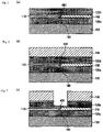
- FIGS. 4( a ) and 4 ( b ) show the side and the upper surface of the optical transmission substrate 10 .
- the core 110 of the optical waveguide 130 is formed in such a manner that the cross section of the core 110 contacts the reflection surface 160 at the end of the optical waveguide 130 .
- polysilane B is applied onto the first substrate 100 , on which the lower clad layer is formed, by spin coating or curtain coating and is pre-baked.
- a layer having a thickness of 50 micrometers is formed.
- the upper surface of the optical transmission substrate 10 is flattened and the following structure is formed. Specifically, in the structure, the core 110 of the optical waveguide 130 , the layer of polysilane B and the reflection surface 160 are buried in the upper surface of the optical transmission substrate 10 , the layer of polysilane B remaining as the clad 120 on the side of the core 110 as a result of being covered up from the ultraviolet rays by the photomask pattern. In addition, the cross section of the core 110 at the end of the optical waveguide 130 contacts the reflection surface 160 .
- FIG. 5 is a fourth view showing the method for manufacturing the optical transmission substrate 10 according to this embodiment.
- the optical transmission substrate 10 may be formed to have a structure in which the clad 120 b above the core 110 at the end of the optical waveguide 130 is thinner than the clad 120 b above the core 110 in the center portion of the optical waveguide 130 .
- the foregoing manufacturing process will be changed as described below.
- polysilane having a thickness of 150 ⁇ m which is equivalent to the thickness of the three layers including the clad 120 a, the core 110 and the clad 120 b, is applied and pre-baked at 120 ⁇ .
- FIGS. 7( b ) and 7 ( c ) by use of a blade 20 having a tilt angle of 45 degrees, the reflection part 150 at an end of a polymer waveguide (PWG) to be the optical waveguide 130 is diced.
- PWG polymer waveguide
- FIG. 8 is a second view showing the method for manufacturing the optical transmission substrate 10 according to the first modified example.
- the optical fiber 170 a is provided in the second substrate 140 and guides the optical signal, which is inputted from the light emitting part 950 , to a position closer to the core 110 than the upper surface of the clad 120 b.
- the reflection surface 160 a is provided on a cross section of the core 110 at a first end of the optical waveguide 130 .
- the reflection surface 160 a reflects the optical signal guided from the upper surface of the second substrate 140 by the optical fiber 170 a and transmits the optical signal through the core 110 of the optical waveguide 130 .
- the reflection surface 160 b is provided on a cross section of the core 110 at a second end of the optical waveguide 130 and reflects the optical signal, which travels through the core 110 of the optical waveguide 130 , toward the second substrate 140 .
- the optical fiber 170 b is provided in the second substrate 140 and guides the optical signal reflected toward the second substrate 140 to the light receiving part 960 from the position closer to the core 110 than the upper surface of the clad 120 b.
Landscapes
- Physics & Mathematics (AREA)
- General Physics & Mathematics (AREA)
- Optics & Photonics (AREA)
- Engineering & Computer Science (AREA)
- Microelectronics & Electronic Packaging (AREA)
- Optical Integrated Circuits (AREA)
- Optical Couplings Of Light Guides (AREA)
- Structure Of Printed Boards (AREA)
Priority Applications (1)
| Application Number | Priority Date | Filing Date | Title |
|---|---|---|---|
| US11/679,460 US7421858B2 (en) | 2003-11-27 | 2007-02-27 | Optical transmission substrate, method for manufacturing optical transmission substrate and optoelectronic integrated circuit |
Applications Claiming Priority (2)
| Application Number | Priority Date | Filing Date | Title |
|---|---|---|---|
| JP2003397920A JP3887371B2 (ja) | 2003-11-27 | 2003-11-27 | 光伝送基板、光伝送基板製造方法、及び光電気集積回路 |
| JP2003-397920 | 2003-11-27 |
Related Child Applications (1)
| Application Number | Title | Priority Date | Filing Date |
|---|---|---|---|
| US11/679,460 Division US7421858B2 (en) | 2003-11-27 | 2007-02-27 | Optical transmission substrate, method for manufacturing optical transmission substrate and optoelectronic integrated circuit |
Publications (2)
| Publication Number | Publication Date |
|---|---|
| US20050117833A1 US20050117833A1 (en) | 2005-06-02 |
| US7212713B2 true US7212713B2 (en) | 2007-05-01 |
Family
ID=34616550
Family Applications (2)
| Application Number | Title | Priority Date | Filing Date |
|---|---|---|---|
| US10/977,170 Active 2025-05-26 US7212713B2 (en) | 2003-11-27 | 2004-10-29 | Optical transmission substrate, method for manufacturing optical transmission substrate and optoelectronic integrated circuit |
| US11/679,460 Expired - Fee Related US7421858B2 (en) | 2003-11-27 | 2007-02-27 | Optical transmission substrate, method for manufacturing optical transmission substrate and optoelectronic integrated circuit |
Family Applications After (1)
| Application Number | Title | Priority Date | Filing Date |
|---|---|---|---|
| US11/679,460 Expired - Fee Related US7421858B2 (en) | 2003-11-27 | 2007-02-27 | Optical transmission substrate, method for manufacturing optical transmission substrate and optoelectronic integrated circuit |
Country Status (2)
| Country | Link |
|---|---|
| US (2) | US7212713B2 (ja) |
| JP (1) | JP3887371B2 (ja) |
Cited By (15)
| Publication number | Priority date | Publication date | Assignee | Title |
|---|---|---|---|---|
| US20070160337A1 (en) * | 2006-01-12 | 2007-07-12 | Samsung Electronics Co., Ltd | Planar light waveguide and method of manufacturing same |
| US20080181557A1 (en) * | 2007-01-31 | 2008-07-31 | Shih-Yuan Wang | Apparatus and method for subterranean distribution of optical signals |
| US20090093073A1 (en) * | 2007-10-09 | 2009-04-09 | Endicott Interconnect Technologies, Inc. | Method of making circuitized substrate with internal optical pathway using photolithography |
| US20090092353A1 (en) * | 2007-10-09 | 2009-04-09 | Endicott Interconnect Technologies, Inc. | Method of making circuitized substrate with internal optical pathway |
| US20090304323A1 (en) * | 2005-04-25 | 2009-12-10 | Takahiro Matsubara | Optical coupling structure and substrate with built-in optical transmission function, and method of manufacturing the same |
| US20100027946A1 (en) * | 2004-02-27 | 2010-02-04 | Banpil Photonics, Inc. | Stackable optoelectronics chip-to-chip interconnects and method of manufacturing |
| US20100201011A1 (en) * | 2007-05-24 | 2010-08-12 | Nitto Denko Corporation | Optical waveguide device and manufacturing method thereof |
| US20110274392A1 (en) * | 2010-05-07 | 2011-11-10 | Fujitsu Limited | Optical transmission apparatus and optical transmission system |
| US20120039576A1 (en) * | 2009-04-08 | 2012-02-16 | International Business Machines Corporation | Optical waveguide with embedded light-reflecting feature and method for fabricating the same |
| US20120251037A1 (en) * | 2011-03-29 | 2012-10-04 | Nitto Denko Corporation | Opto-electric hybrid board and manufacturing method therefor |
| US10025033B2 (en) | 2016-03-01 | 2018-07-17 | Advanced Semiconductor Engineering, Inc. | Optical fiber structure, optical communication apparatus and manufacturing process for manufacturing the same |
| US10241264B2 (en) | 2016-07-01 | 2019-03-26 | Advanced Semiconductor Engineering, Inc. | Semiconductor device packages |
| US10754113B1 (en) | 2019-08-16 | 2020-08-25 | Eagle Technology, Llc | Opto-electronic device including active circuit component on circuit attachment area of optical fiber and related methods |
| US20210132309A1 (en) * | 2019-10-31 | 2021-05-06 | Ayar Labs, Inc. | Vertical Integrated Photonics Chiplet for In-Package Optical Interconnect |
| US11262605B2 (en) * | 2017-08-31 | 2022-03-01 | Lightwave Logic Inc. | Active region-less polymer modulator integrated on a common PIC platform and method |
Families Citing this family (28)
| Publication number | Priority date | Publication date | Assignee | Title |
|---|---|---|---|---|
| FR2890456B1 (fr) * | 2005-09-02 | 2009-06-12 | Commissariat Energie Atomique | Dispositif de couplage hermetique |
| JP2007093740A (ja) * | 2005-09-27 | 2007-04-12 | Mitsumi Electric Co Ltd | 光導波路デバイス |
| JP5332079B2 (ja) * | 2006-03-08 | 2013-11-06 | 凸版印刷株式会社 | 球状弾性表面波素子の製造方法 |
| JP4967803B2 (ja) * | 2006-05-18 | 2012-07-04 | 凸版印刷株式会社 | 光電気複合基板の製造方法 |
| JP2008015303A (ja) * | 2006-07-07 | 2008-01-24 | Toppan Printing Co Ltd | 光基板及びその製造方法 |
| JP5137393B2 (ja) * | 2006-12-19 | 2013-02-06 | 古河電気工業株式会社 | 光結合器 |
| US7421160B1 (en) * | 2007-04-10 | 2008-09-02 | International Business Machines Corporation | Coupling element alignment using waveguide fiducials |
| JP5018254B2 (ja) * | 2007-06-06 | 2012-09-05 | 日立電線株式会社 | ミラー付き光導波路及びその製造方法 |
| JP2009288614A (ja) * | 2008-05-30 | 2009-12-10 | Hitachi Ltd | 平面型光導波路アレイモジュールとその製造方法 |
| JP5109982B2 (ja) * | 2008-10-09 | 2012-12-26 | 日立電線株式会社 | ミラー付き光伝送体の製造方法 |
| US8164986B2 (en) * | 2009-05-26 | 2012-04-24 | Tdk Corporation | Thermally-assisted magnetic recording head and thermally-assisted magnetic recording method |
| CN102933998B (zh) * | 2010-06-07 | 2015-06-17 | Fci公司 | 光学系统 |
| US8708576B2 (en) | 2011-01-20 | 2014-04-29 | Harris Corporation | Electro-optical device having an elastomeric body and related methods |
| JPWO2012114907A1 (ja) * | 2011-02-23 | 2014-07-07 | コニカミノルタ株式会社 | 有機エレクトロルミネッセンス素子の製造方法 |
| JP2013097004A (ja) * | 2011-10-27 | 2013-05-20 | Kyocera Corp | 光配線基板および光配線装置 |
| WO2013085225A1 (en) * | 2011-12-08 | 2013-06-13 | Lg Innotek Co., Ltd. | Optical printed circuit board and method of manufacturing the same |
| KR101856229B1 (ko) * | 2011-12-09 | 2018-05-09 | 엘지이노텍 주식회사 | 광 인쇄회로기판 및 그의 제조 방법 |
| KR101856230B1 (ko) * | 2011-12-09 | 2018-05-09 | 엘지이노텍 주식회사 | 광 인쇄회로기판 및 그의 제조 방법 |
| US20140272315A1 (en) * | 2013-03-15 | 2014-09-18 | Tyco Electronics Corporation | Method for fabricating negative photoresist etched pits and trenches as controlled optical path and a device fabricated thereby |
| US9170386B2 (en) | 2013-04-08 | 2015-10-27 | Hon Hai Precision Industry Co., Ltd. | Opto-electronic device assembly |
| CN103760635B (zh) * | 2014-01-28 | 2015-10-14 | 华进半导体封装先导技术研发中心有限公司 | 玻璃基三维光电同传器件及其制作方法 |
| JP6677654B2 (ja) * | 2014-05-23 | 2020-04-08 | ナノプレシジョン プロダクツ インコーポレイテッドNanoprecision Products, Inc. | 光電子デバイスに対する光ファイバサブアセンブリの視覚に基づく受動的位置決め |
| JP6623344B2 (ja) * | 2016-03-22 | 2019-12-25 | 日東電工株式会社 | 光導波路積層体およびその製法 |
| US10705302B2 (en) * | 2018-02-27 | 2020-07-07 | Samsung Electronics Co., Ltd. | Photonic integrated circuit packages |
| US11520044B2 (en) * | 2018-09-25 | 2022-12-06 | Waymo Llc | Waveguide diffusers for LIDARs |
| US11768338B2 (en) * | 2021-05-27 | 2023-09-26 | Taiwan Semiconductor Manufacturing Company, Ltd. | Optical interconnect structure, package structure and fabricating method thereof |
| US11867956B2 (en) * | 2021-08-19 | 2024-01-09 | Advanced Semiconductor Engineering, Inc. | Optoelectronic device |
| US20230123286A1 (en) * | 2021-10-15 | 2023-04-20 | QuantumZ Inc. | Transmission device for guiding transmission signal |
Citations (13)
| Publication number | Priority date | Publication date | Assignee | Title |
|---|---|---|---|---|
| US5125054A (en) * | 1991-07-25 | 1992-06-23 | Motorola, Inc. | Laminated polymer optical waveguide interface and method of making same |
| JPH11119034A (ja) | 1997-10-15 | 1999-04-30 | Nippon Telegr & Teleph Corp <Ntt> | 光配線板製造装置 |
| JPH11119033A (ja) | 1997-10-15 | 1999-04-30 | Nippon Telegr & Teleph Corp <Ntt> | 光配線板及び光配線板の配線方法 |
| JP2000047044A (ja) | 1998-07-31 | 2000-02-18 | Sony Corp | 光信号伝送システムおよびその製造方法 |
| JP2000081524A (ja) | 1998-09-07 | 2000-03-21 | Sony Corp | 光送受信システム |
| JP2000227524A (ja) | 1999-02-05 | 2000-08-15 | Sony Corp | 光導波装置および光送受信装置、ならびにそれらの製造方法 |
| JP2000235127A (ja) | 1999-02-15 | 2000-08-29 | Nippon Telegr & Teleph Corp <Ntt> | 光電子集積回路およびその作製方法 |
| US20020051599A1 (en) * | 1999-06-25 | 2002-05-02 | Toppan Printing Co., Ltd. | Optical-electrical wiring board, mounted board and method of manufacturing optical-electrical wiring board |
| US20020097962A1 (en) * | 1998-10-09 | 2002-07-25 | Tetsuzo Yoshimura | Single and multilayer waveguides and fabrication process |
| US6847765B2 (en) * | 2002-03-15 | 2005-01-25 | Agilent Technologies, Inc. | Re-connectable optical interface system and method for optically interconnecting and disconnecting optical devices |
| US20050175273A1 (en) * | 2002-08-02 | 2005-08-11 | Kazuhiro Iida | Microchip, method of manufacturing microchip, and method of detecting compositions |
| US20060008199A1 (en) * | 2004-07-09 | 2006-01-12 | Alexei Glebov | Optical apparatuses providing optical interconnections among a plurality of electronic components |
| US20060210213A1 (en) * | 2005-03-15 | 2006-09-21 | Lidu Huang | Optical backplanes with integrated optical couplers and methods of making the same |
Family Cites Families (2)
| Publication number | Priority date | Publication date | Assignee | Title |
|---|---|---|---|---|
| JP2002258081A (ja) * | 2001-02-28 | 2002-09-11 | Fujitsu Ltd | 光配線基板、光配線基板の製造方法及び多層光配線 |
| US7221826B2 (en) * | 2002-10-08 | 2007-05-22 | Tdk Corporation | Spot-size transformer, method of producing spot-size transformer and waveguide-embedded optical circuit using spot-size transformer |
-
2003
- 2003-11-27 JP JP2003397920A patent/JP3887371B2/ja not_active Expired - Lifetime
-
2004
- 2004-10-29 US US10/977,170 patent/US7212713B2/en active Active
-
2007
- 2007-02-27 US US11/679,460 patent/US7421858B2/en not_active Expired - Fee Related
Patent Citations (14)
| Publication number | Priority date | Publication date | Assignee | Title |
|---|---|---|---|---|
| US5125054A (en) * | 1991-07-25 | 1992-06-23 | Motorola, Inc. | Laminated polymer optical waveguide interface and method of making same |
| JPH11119034A (ja) | 1997-10-15 | 1999-04-30 | Nippon Telegr & Teleph Corp <Ntt> | 光配線板製造装置 |
| JPH11119033A (ja) | 1997-10-15 | 1999-04-30 | Nippon Telegr & Teleph Corp <Ntt> | 光配線板及び光配線板の配線方法 |
| JP2000047044A (ja) | 1998-07-31 | 2000-02-18 | Sony Corp | 光信号伝送システムおよびその製造方法 |
| US6330377B1 (en) * | 1998-09-07 | 2001-12-11 | Sony Corporation | Optical transmitting/receiving method and apparatus |
| JP2000081524A (ja) | 1998-09-07 | 2000-03-21 | Sony Corp | 光送受信システム |
| US20020097962A1 (en) * | 1998-10-09 | 2002-07-25 | Tetsuzo Yoshimura | Single and multilayer waveguides and fabrication process |
| JP2000227524A (ja) | 1999-02-05 | 2000-08-15 | Sony Corp | 光導波装置および光送受信装置、ならびにそれらの製造方法 |
| JP2000235127A (ja) | 1999-02-15 | 2000-08-29 | Nippon Telegr & Teleph Corp <Ntt> | 光電子集積回路およびその作製方法 |
| US20020051599A1 (en) * | 1999-06-25 | 2002-05-02 | Toppan Printing Co., Ltd. | Optical-electrical wiring board, mounted board and method of manufacturing optical-electrical wiring board |
| US6847765B2 (en) * | 2002-03-15 | 2005-01-25 | Agilent Technologies, Inc. | Re-connectable optical interface system and method for optically interconnecting and disconnecting optical devices |
| US20050175273A1 (en) * | 2002-08-02 | 2005-08-11 | Kazuhiro Iida | Microchip, method of manufacturing microchip, and method of detecting compositions |
| US20060008199A1 (en) * | 2004-07-09 | 2006-01-12 | Alexei Glebov | Optical apparatuses providing optical interconnections among a plurality of electronic components |
| US20060210213A1 (en) * | 2005-03-15 | 2006-09-21 | Lidu Huang | Optical backplanes with integrated optical couplers and methods of making the same |
Non-Patent Citations (5)
| Title |
|---|
| Cregan et al., "Single Mode Photonic Band Gap Guidance of Light in Air", Science, vol. 285, Sep. 3, 1999, pp. 1537-1539. |
| Ishii et al., "Large-Tolerant OptoBump Interface For Interchip Optical Interconnections" vol. J84-C, No. 9, 2001, pp. 793-799. (No English Translation). |
| Mikami et al., "Development of Optical Surface Mount Technology", vol. J84-C, No. 9, 2001, pp. 715-726. (No English Translation). |
| Offrein et al., "Tunable WDM Add/Drop Components in Silicon-Oxynitride Waveguide Technology", Electronic Components and Technology Conference, 1999, pp. 19-25. |
| T. Maruno, "Polymer Optical Waveguide Devices", Technical Report of IEICE, 1999, pp. 1-6. |
Cited By (27)
| Publication number | Priority date | Publication date | Assignee | Title |
|---|---|---|---|---|
| US7923273B2 (en) * | 2004-02-27 | 2011-04-12 | Banpil Photonics, Inc. | Stackable optoelectronics chip-to-chip interconnects and method of manufacturing |
| US20100027946A1 (en) * | 2004-02-27 | 2010-02-04 | Banpil Photonics, Inc. | Stackable optoelectronics chip-to-chip interconnects and method of manufacturing |
| US20090304323A1 (en) * | 2005-04-25 | 2009-12-10 | Takahiro Matsubara | Optical coupling structure and substrate with built-in optical transmission function, and method of manufacturing the same |
| US20070160337A1 (en) * | 2006-01-12 | 2007-07-12 | Samsung Electronics Co., Ltd | Planar light waveguide and method of manufacturing same |
| US7639912B2 (en) * | 2007-01-31 | 2009-12-29 | Hewlett-Packard Development Company, L.P. | Apparatus and method for subterranean distribution of optical signals |
| US20080181557A1 (en) * | 2007-01-31 | 2008-07-31 | Shih-Yuan Wang | Apparatus and method for subterranean distribution of optical signals |
| US8744220B2 (en) | 2007-05-24 | 2014-06-03 | Nitto Denko Corporation | Optical waveguide device and manufacturing method thereof |
| US20100201011A1 (en) * | 2007-05-24 | 2010-08-12 | Nitto Denko Corporation | Optical waveguide device and manufacturing method thereof |
| US7541058B2 (en) | 2007-10-09 | 2009-06-02 | Endicott Interconnect Technologies, Inc. | Method of making circuitized substrate with internal optical pathway |
| US20090093073A1 (en) * | 2007-10-09 | 2009-04-09 | Endicott Interconnect Technologies, Inc. | Method of making circuitized substrate with internal optical pathway using photolithography |
| US7713767B2 (en) | 2007-10-09 | 2010-05-11 | Endicott Interconnect Technologies, Inc. | Method of making circuitized substrate with internal optical pathway using photolithography |
| EP2048526A2 (en) | 2007-10-09 | 2009-04-15 | Endicott Interconnect Technologies, Inc. | Method of making circuitized substrate with internal optical pathway using photolithography |
| US20090092353A1 (en) * | 2007-10-09 | 2009-04-09 | Endicott Interconnect Technologies, Inc. | Method of making circuitized substrate with internal optical pathway |
| EP2048527A2 (en) | 2007-10-09 | 2009-04-15 | Endicott Interconnect Technologies, Inc. | Method of making circuitized substrate with internal optical pathway |
| US20120039576A1 (en) * | 2009-04-08 | 2012-02-16 | International Business Machines Corporation | Optical waveguide with embedded light-reflecting feature and method for fabricating the same |
| US8873912B2 (en) * | 2009-04-08 | 2014-10-28 | International Business Machines Corporation | Optical waveguide with embedded light-reflecting feature and method for fabricating the same |
| US20110274392A1 (en) * | 2010-05-07 | 2011-11-10 | Fujitsu Limited | Optical transmission apparatus and optical transmission system |
| US8783971B2 (en) * | 2010-05-07 | 2014-07-22 | Fujitsu Limited | Optical transmission apparatus and optical transmission system |
| US8606056B2 (en) * | 2011-03-29 | 2013-12-10 | Nitto Denko Corporation | Opto-electric hybrid board and manufacturing method therefor |
| US20120251037A1 (en) * | 2011-03-29 | 2012-10-04 | Nitto Denko Corporation | Opto-electric hybrid board and manufacturing method therefor |
| US10025033B2 (en) | 2016-03-01 | 2018-07-17 | Advanced Semiconductor Engineering, Inc. | Optical fiber structure, optical communication apparatus and manufacturing process for manufacturing the same |
| US10241264B2 (en) | 2016-07-01 | 2019-03-26 | Advanced Semiconductor Engineering, Inc. | Semiconductor device packages |
| US10838144B2 (en) | 2016-07-01 | 2020-11-17 | Advanced Semiconductor Engineering, Inc. | Semiconductor device packages |
| US11262605B2 (en) * | 2017-08-31 | 2022-03-01 | Lightwave Logic Inc. | Active region-less polymer modulator integrated on a common PIC platform and method |
| US10754113B1 (en) | 2019-08-16 | 2020-08-25 | Eagle Technology, Llc | Opto-electronic device including active circuit component on circuit attachment area of optical fiber and related methods |
| US20210132309A1 (en) * | 2019-10-31 | 2021-05-06 | Ayar Labs, Inc. | Vertical Integrated Photonics Chiplet for In-Package Optical Interconnect |
| US11899251B2 (en) * | 2019-10-31 | 2024-02-13 | Ayar Labs, Inc. | Vertical integrated photonics chiplet for in-package optical interconnect |
Also Published As
| Publication number | Publication date |
|---|---|
| US7421858B2 (en) | 2008-09-09 |
| JP3887371B2 (ja) | 2007-02-28 |
| US20050117833A1 (en) | 2005-06-02 |
| JP2005157128A (ja) | 2005-06-16 |
| US20070137254A1 (en) | 2007-06-21 |
Similar Documents
| Publication | Publication Date | Title |
|---|---|---|
| US7212713B2 (en) | Optical transmission substrate, method for manufacturing optical transmission substrate and optoelectronic integrated circuit | |
| US7590315B2 (en) | Optical waveguide and optical module using the same | |
| KR100720854B1 (ko) | 광·전기배선기판, 실장기판 및 광전기배선기판의 제조방법 | |
| JP4690870B2 (ja) | 光電気集積配線基板及び光電気集積配線システム | |
| JP2007072007A (ja) | 光導波路モジュール | |
| US20090214156A1 (en) | Optical module and optical waveguide | |
| JP2006209068A (ja) | 光導波路、光導波路モジュール及び光導波路モジュールの製造方法 | |
| JP2002169042A (ja) | 光導波路結合構造、光導波路及びその製造方法、並びに光導波路付き光素子部品及びその製造方法 | |
| JP2008102283A (ja) | 光導波路、光モジュール及び光導波路の製造方法 | |
| US6608946B2 (en) | Optical module and method for manufacturing the same | |
| JP5078442B2 (ja) | 光伝送基板およびその製造方法、並びに光電子混載基板および光モジュール | |
| US6516105B1 (en) | Optical backplane assembly and method of making same | |
| JP2007183467A (ja) | ミラー付光導波路及びその製造方法 | |
| JP2007505355A (ja) | 導波路形成方法及びそれで形成された導波路 | |
| JP2008134492A (ja) | 光伝送システムおよびそれを具備する光モジュール | |
| JP2005070141A (ja) | 光路変換部品付きの光導波路構造体及びその製造方法、光路変換部品 | |
| JP2008275770A (ja) | 光路変換体、光路変換構造、複合光伝送基板および光モジュール | |
| JP2006310417A (ja) | 光電変換装置及びその製造方法、並びに光情報処理装置 | |
| JP2006178282A (ja) | 光導波路樹脂フィルムおよびそれを用いた光配線部材 | |
| JP2007041122A (ja) | ポリマ光導波路の製造方法及びポリマ光導波路、並びにそれを用いた光モジュール | |
| JP2006052992A (ja) | 光導波路配線基板又は光電気混載基板の検査方法 | |
| JP6280069B2 (ja) | 光導波路回路および光デバイス | |
| JP2003270461A (ja) | 光通信部品、積層型光通信モジュール、およびその製造方法 | |
| JP2019028116A (ja) | 光導波路、光導波路接続体および電子機器 | |
| JP2005338704A (ja) | 光結合機能付配線基板及びその製造方法と光結合システム |
Legal Events
| Date | Code | Title | Description |
|---|---|---|---|
| AS | Assignment |
Owner name: INTERNATIONAL BUSINESS MACHINES CORPORATION, NEW Y Free format text: ASSIGNMENT OF ASSIGNORS INTEREST;ASSIGNORS:FUKUZAWA, TADASHI;HASEGAWA, MASAKI;REEL/FRAME:015941/0841;SIGNING DATES FROM 20041014 TO 20041015 |
|
| FEPP | Fee payment procedure |
Free format text: PAYOR NUMBER ASSIGNED (ORIGINAL EVENT CODE: ASPN); ENTITY STATUS OF PATENT OWNER: LARGE ENTITY |
|
| STCF | Information on status: patent grant |
Free format text: PATENTED CASE |
|
| FPAY | Fee payment |
Year of fee payment: 4 |
|
| FPAY | Fee payment |
Year of fee payment: 8 |
|
| MAFP | Maintenance fee payment |
Free format text: PAYMENT OF MAINTENANCE FEE, 12TH YEAR, LARGE ENTITY (ORIGINAL EVENT CODE: M1553); ENTITY STATUS OF PATENT OWNER: LARGE ENTITY Year of fee payment: 12 |