US7157361B2 - Methods for processing integrated circuit packages formed using electroplating and apparatus made therefrom - Google Patents
Methods for processing integrated circuit packages formed using electroplating and apparatus made therefrom Download PDFInfo
- Publication number
- US7157361B2 US7157361B2 US10/878,157 US87815704A US7157361B2 US 7157361 B2 US7157361 B2 US 7157361B2 US 87815704 A US87815704 A US 87815704A US 7157361 B2 US7157361 B2 US 7157361B2
- Authority
- US
- United States
- Prior art keywords
- integrated circuit
- circuit package
- electroplating
- back plane
- pad
- Prior art date
- Legal status (The legal status is an assumption and is not a legal conclusion. Google has not performed a legal analysis and makes no representation as to the accuracy of the status listed.)
- Active, expires
Links
- 238000009713 electroplating Methods 0.000 title claims abstract description 72
- 238000000034 method Methods 0.000 title claims description 50
- 238000007747 plating Methods 0.000 claims abstract description 47
- 239000000463 material Substances 0.000 claims abstract description 24
- 238000000059 patterning Methods 0.000 claims abstract description 12
- 230000008878 coupling Effects 0.000 claims description 24
- 238000010168 coupling process Methods 0.000 claims description 24
- 238000005859 coupling reaction Methods 0.000 claims description 24
- PXHVJJICTQNCMI-UHFFFAOYSA-N Nickel Chemical compound [Ni] PXHVJJICTQNCMI-UHFFFAOYSA-N 0.000 claims description 22
- PCHJSUWPFVWCPO-UHFFFAOYSA-N gold Chemical compound [Au] PCHJSUWPFVWCPO-UHFFFAOYSA-N 0.000 claims description 11
- 229910052737 gold Inorganic materials 0.000 claims description 11
- 239000010931 gold Substances 0.000 claims description 11
- 229910052759 nickel Inorganic materials 0.000 claims description 11
- 230000008569 process Effects 0.000 claims description 10
- 238000004806 packaging method and process Methods 0.000 claims description 3
- RYGMFSIKBFXOCR-UHFFFAOYSA-N Copper Chemical compound [Cu] RYGMFSIKBFXOCR-UHFFFAOYSA-N 0.000 description 28
- 229910052802 copper Inorganic materials 0.000 description 26
- 239000010949 copper Substances 0.000 description 26
- 229910000679 solder Inorganic materials 0.000 description 15
- 238000010586 diagram Methods 0.000 description 3
- 239000011889 copper foil Substances 0.000 description 2
- 238000005530 etching Methods 0.000 description 2
- ZEMPKEQAKRGZGQ-AAKVHIHISA-N 2,3-bis[[(z)-12-hydroxyoctadec-9-enoyl]oxy]propyl (z)-12-hydroxyoctadec-9-enoate Chemical compound CCCCCCC(O)C\C=C/CCCCCCCC(=O)OCC(OC(=O)CCCCCCC\C=C/CC(O)CCCCCC)COC(=O)CCCCCCC\C=C/CC(O)CCCCCC ZEMPKEQAKRGZGQ-AAKVHIHISA-N 0.000 description 1
- 239000000853 adhesive Substances 0.000 description 1
- 230000001070 adhesive effect Effects 0.000 description 1
- 230000008859 change Effects 0.000 description 1
- 238000007796 conventional method Methods 0.000 description 1
- 239000003989 dielectric material Substances 0.000 description 1
- 238000007772 electroless plating Methods 0.000 description 1
- 229910052751 metal Inorganic materials 0.000 description 1
- 239000002184 metal Substances 0.000 description 1
- 150000002739 metals Chemical class 0.000 description 1
- 238000012986 modification Methods 0.000 description 1
- 230000004048 modification Effects 0.000 description 1
Images


Classifications
-
- H—ELECTRICITY
- H01—ELECTRIC ELEMENTS
- H01L—SEMICONDUCTOR DEVICES NOT COVERED BY CLASS H10
- H01L23/00—Details of semiconductor or other solid state devices
- H01L23/48—Arrangements for conducting electric current to or from the solid state body in operation, e.g. leads, terminal arrangements ; Selection of materials therefor
- H01L23/488—Arrangements for conducting electric current to or from the solid state body in operation, e.g. leads, terminal arrangements ; Selection of materials therefor consisting of soldered or bonded constructions
- H01L23/498—Leads, i.e. metallisations or lead-frames on insulating substrates, e.g. chip carriers
- H01L23/49805—Leads, i.e. metallisations or lead-frames on insulating substrates, e.g. chip carriers the leads being also applied on the sidewalls or the bottom of the substrate, e.g. leadless packages for surface mounting
-
- H—ELECTRICITY
- H01—ELECTRIC ELEMENTS
- H01L—SEMICONDUCTOR DEVICES NOT COVERED BY CLASS H10
- H01L21/00—Processes or apparatus adapted for the manufacture or treatment of semiconductor or solid state devices or of parts thereof
- H01L21/02—Manufacture or treatment of semiconductor devices or of parts thereof
- H01L21/04—Manufacture or treatment of semiconductor devices or of parts thereof the devices having potential barriers, e.g. a PN junction, depletion layer or carrier concentration layer
- H01L21/48—Manufacture or treatment of parts, e.g. containers, prior to assembly of the devices, using processes not provided for in a single one of the subgroups H01L21/06 - H01L21/326
- H01L21/4814—Conductive parts
- H01L21/4846—Leads on or in insulating or insulated substrates, e.g. metallisation
-
- H—ELECTRICITY
- H01—ELECTRIC ELEMENTS
- H01L—SEMICONDUCTOR DEVICES NOT COVERED BY CLASS H10
- H01L23/00—Details of semiconductor or other solid state devices
- H01L23/48—Arrangements for conducting electric current to or from the solid state body in operation, e.g. leads, terminal arrangements ; Selection of materials therefor
- H01L23/488—Arrangements for conducting electric current to or from the solid state body in operation, e.g. leads, terminal arrangements ; Selection of materials therefor consisting of soldered or bonded constructions
- H01L23/498—Leads, i.e. metallisations or lead-frames on insulating substrates, e.g. chip carriers
- H01L23/49838—Geometry or layout
-
- H—ELECTRICITY
- H01—ELECTRIC ELEMENTS
- H01L—SEMICONDUCTOR DEVICES NOT COVERED BY CLASS H10
- H01L23/00—Details of semiconductor or other solid state devices
- H01L23/52—Arrangements for conducting electric current within the device in operation from one component to another, i.e. interconnections, e.g. wires, lead frames
-
- H—ELECTRICITY
- H05—ELECTRIC TECHNIQUES NOT OTHERWISE PROVIDED FOR
- H05K—PRINTED CIRCUITS; CASINGS OR CONSTRUCTIONAL DETAILS OF ELECTRIC APPARATUS; MANUFACTURE OF ASSEMBLAGES OF ELECTRICAL COMPONENTS
- H05K3/00—Apparatus or processes for manufacturing printed circuits
- H05K3/22—Secondary treatment of printed circuits
- H05K3/24—Reinforcing the conductive pattern
- H05K3/241—Reinforcing the conductive pattern characterised by the electroplating method; means therefor, e.g. baths or apparatus
- H05K3/242—Reinforcing the conductive pattern characterised by the electroplating method; means therefor, e.g. baths or apparatus characterised by using temporary conductors on the printed circuit for electrically connecting areas which are to be electroplated
-
- H—ELECTRICITY
- H01—ELECTRIC ELEMENTS
- H01L—SEMICONDUCTOR DEVICES NOT COVERED BY CLASS H10
- H01L2224/00—Indexing scheme for arrangements for connecting or disconnecting semiconductor or solid-state bodies and methods related thereto as covered by H01L24/00
- H01L2224/01—Means for bonding being attached to, or being formed on, the surface to be connected, e.g. chip-to-package, die-attach, "first-level" interconnects; Manufacturing methods related thereto
- H01L2224/42—Wire connectors; Manufacturing methods related thereto
- H01L2224/44—Structure, shape, material or disposition of the wire connectors prior to the connecting process
- H01L2224/45—Structure, shape, material or disposition of the wire connectors prior to the connecting process of an individual wire connector
- H01L2224/45001—Core members of the connector
- H01L2224/45099—Material
- H01L2224/451—Material with a principal constituent of the material being a metal or a metalloid, e.g. boron (B), silicon (Si), germanium (Ge), arsenic (As), antimony (Sb), tellurium (Te) and polonium (Po), and alloys thereof
- H01L2224/45138—Material with a principal constituent of the material being a metal or a metalloid, e.g. boron (B), silicon (Si), germanium (Ge), arsenic (As), antimony (Sb), tellurium (Te) and polonium (Po), and alloys thereof the principal constituent melting at a temperature of greater than or equal to 950°C and less than 1550°C
- H01L2224/45144—Gold (Au) as principal constituent
-
- H—ELECTRICITY
- H01—ELECTRIC ELEMENTS
- H01L—SEMICONDUCTOR DEVICES NOT COVERED BY CLASS H10
- H01L2224/00—Indexing scheme for arrangements for connecting or disconnecting semiconductor or solid-state bodies and methods related thereto as covered by H01L24/00
- H01L2224/01—Means for bonding being attached to, or being formed on, the surface to be connected, e.g. chip-to-package, die-attach, "first-level" interconnects; Manufacturing methods related thereto
- H01L2224/42—Wire connectors; Manufacturing methods related thereto
- H01L2224/47—Structure, shape, material or disposition of the wire connectors after the connecting process
- H01L2224/48—Structure, shape, material or disposition of the wire connectors after the connecting process of an individual wire connector
- H01L2224/4805—Shape
- H01L2224/4809—Loop shape
- H01L2224/48091—Arched
-
- H—ELECTRICITY
- H01—ELECTRIC ELEMENTS
- H01L—SEMICONDUCTOR DEVICES NOT COVERED BY CLASS H10
- H01L2224/00—Indexing scheme for arrangements for connecting or disconnecting semiconductor or solid-state bodies and methods related thereto as covered by H01L24/00
- H01L2224/01—Means for bonding being attached to, or being formed on, the surface to be connected, e.g. chip-to-package, die-attach, "first-level" interconnects; Manufacturing methods related thereto
- H01L2224/42—Wire connectors; Manufacturing methods related thereto
- H01L2224/47—Structure, shape, material or disposition of the wire connectors after the connecting process
- H01L2224/48—Structure, shape, material or disposition of the wire connectors after the connecting process of an individual wire connector
- H01L2224/481—Disposition
- H01L2224/48151—Connecting between a semiconductor or solid-state body and an item not being a semiconductor or solid-state body, e.g. chip-to-substrate, chip-to-passive
- H01L2224/48221—Connecting between a semiconductor or solid-state body and an item not being a semiconductor or solid-state body, e.g. chip-to-substrate, chip-to-passive the body and the item being stacked
- H01L2224/48225—Connecting between a semiconductor or solid-state body and an item not being a semiconductor or solid-state body, e.g. chip-to-substrate, chip-to-passive the body and the item being stacked the item being non-metallic, e.g. insulating substrate with or without metallisation
- H01L2224/48227—Connecting between a semiconductor or solid-state body and an item not being a semiconductor or solid-state body, e.g. chip-to-substrate, chip-to-passive the body and the item being stacked the item being non-metallic, e.g. insulating substrate with or without metallisation connecting the wire to a bond pad of the item
-
- H—ELECTRICITY
- H01—ELECTRIC ELEMENTS
- H01L—SEMICONDUCTOR DEVICES NOT COVERED BY CLASS H10
- H01L23/00—Details of semiconductor or other solid state devices
- H01L23/34—Arrangements for cooling, heating, ventilating or temperature compensation ; Temperature sensing arrangements
- H01L23/36—Selection of materials, or shaping, to facilitate cooling or heating, e.g. heatsinks
-
- H—ELECTRICITY
- H01—ELECTRIC ELEMENTS
- H01L—SEMICONDUCTOR DEVICES NOT COVERED BY CLASS H10
- H01L24/00—Arrangements for connecting or disconnecting semiconductor or solid-state bodies; Methods or apparatus related thereto
- H01L24/01—Means for bonding being attached to, or being formed on, the surface to be connected, e.g. chip-to-package, die-attach, "first-level" interconnects; Manufacturing methods related thereto
- H01L24/42—Wire connectors; Manufacturing methods related thereto
- H01L24/44—Structure, shape, material or disposition of the wire connectors prior to the connecting process
- H01L24/45—Structure, shape, material or disposition of the wire connectors prior to the connecting process of an individual wire connector
-
- H—ELECTRICITY
- H01—ELECTRIC ELEMENTS
- H01L—SEMICONDUCTOR DEVICES NOT COVERED BY CLASS H10
- H01L24/00—Arrangements for connecting or disconnecting semiconductor or solid-state bodies; Methods or apparatus related thereto
- H01L24/01—Means for bonding being attached to, or being formed on, the surface to be connected, e.g. chip-to-package, die-attach, "first-level" interconnects; Manufacturing methods related thereto
- H01L24/42—Wire connectors; Manufacturing methods related thereto
- H01L24/47—Structure, shape, material or disposition of the wire connectors after the connecting process
- H01L24/48—Structure, shape, material or disposition of the wire connectors after the connecting process of an individual wire connector
-
- H—ELECTRICITY
- H01—ELECTRIC ELEMENTS
- H01L—SEMICONDUCTOR DEVICES NOT COVERED BY CLASS H10
- H01L2924/00—Indexing scheme for arrangements or methods for connecting or disconnecting semiconductor or solid-state bodies as covered by H01L24/00
- H01L2924/0001—Technical content checked by a classifier
- H01L2924/00014—Technical content checked by a classifier the subject-matter covered by the group, the symbol of which is combined with the symbol of this group, being disclosed without further technical details
-
- H—ELECTRICITY
- H01—ELECTRIC ELEMENTS
- H01L—SEMICONDUCTOR DEVICES NOT COVERED BY CLASS H10
- H01L2924/00—Indexing scheme for arrangements or methods for connecting or disconnecting semiconductor or solid-state bodies as covered by H01L24/00
- H01L2924/01—Chemical elements
- H01L2924/01078—Platinum [Pt]
-
- H—ELECTRICITY
- H01—ELECTRIC ELEMENTS
- H01L—SEMICONDUCTOR DEVICES NOT COVERED BY CLASS H10
- H01L2924/00—Indexing scheme for arrangements or methods for connecting or disconnecting semiconductor or solid-state bodies as covered by H01L24/00
- H01L2924/01—Chemical elements
- H01L2924/01079—Gold [Au]
-
- H—ELECTRICITY
- H01—ELECTRIC ELEMENTS
- H01L—SEMICONDUCTOR DEVICES NOT COVERED BY CLASS H10
- H01L2924/00—Indexing scheme for arrangements or methods for connecting or disconnecting semiconductor or solid-state bodies as covered by H01L24/00
- H01L2924/10—Details of semiconductor or other solid state devices to be connected
- H01L2924/11—Device type
- H01L2924/14—Integrated circuits
-
- H—ELECTRICITY
- H01—ELECTRIC ELEMENTS
- H01L—SEMICONDUCTOR DEVICES NOT COVERED BY CLASS H10
- H01L2924/00—Indexing scheme for arrangements or methods for connecting or disconnecting semiconductor or solid-state bodies as covered by H01L24/00
- H01L2924/15—Details of package parts other than the semiconductor or other solid state devices to be connected
- H01L2924/151—Die mounting substrate
- H01L2924/1515—Shape
- H01L2924/15153—Shape the die mounting substrate comprising a recess for hosting the device
-
- H—ELECTRICITY
- H01—ELECTRIC ELEMENTS
- H01L—SEMICONDUCTOR DEVICES NOT COVERED BY CLASS H10
- H01L2924/00—Indexing scheme for arrangements or methods for connecting or disconnecting semiconductor or solid-state bodies as covered by H01L24/00
- H01L2924/15—Details of package parts other than the semiconductor or other solid state devices to be connected
- H01L2924/151—Die mounting substrate
- H01L2924/1517—Multilayer substrate
-
- H—ELECTRICITY
- H01—ELECTRIC ELEMENTS
- H01L—SEMICONDUCTOR DEVICES NOT COVERED BY CLASS H10
- H01L2924/00—Indexing scheme for arrangements or methods for connecting or disconnecting semiconductor or solid-state bodies as covered by H01L24/00
- H01L2924/15—Details of package parts other than the semiconductor or other solid state devices to be connected
- H01L2924/151—Die mounting substrate
- H01L2924/153—Connection portion
- H01L2924/1531—Connection portion the connection portion being formed only on the surface of the substrate opposite to the die mounting surface
- H01L2924/15311—Connection portion the connection portion being formed only on the surface of the substrate opposite to the die mounting surface being a ball array, e.g. BGA
-
- H—ELECTRICITY
- H01—ELECTRIC ELEMENTS
- H01L—SEMICONDUCTOR DEVICES NOT COVERED BY CLASS H10
- H01L2924/00—Indexing scheme for arrangements or methods for connecting or disconnecting semiconductor or solid-state bodies as covered by H01L24/00
- H01L2924/15—Details of package parts other than the semiconductor or other solid state devices to be connected
- H01L2924/151—Die mounting substrate
- H01L2924/153—Connection portion
- H01L2924/1532—Connection portion the connection portion being formed on the die mounting surface of the substrate
-
- H—ELECTRICITY
- H05—ELECTRIC TECHNIQUES NOT OTHERWISE PROVIDED FOR
- H05K—PRINTED CIRCUITS; CASINGS OR CONSTRUCTIONAL DETAILS OF ELECTRIC APPARATUS; MANUFACTURE OF ASSEMBLAGES OF ELECTRICAL COMPONENTS
- H05K2201/00—Indexing scheme relating to printed circuits covered by H05K1/00
- H05K2201/09—Shape and layout
- H05K2201/09209—Shape and layout details of conductors
- H05K2201/09372—Pads and lands
- H05K2201/0949—Pad close to a hole, not surrounding the hole
-
- H—ELECTRICITY
- H05—ELECTRIC TECHNIQUES NOT OTHERWISE PROVIDED FOR
- H05K—PRINTED CIRCUITS; CASINGS OR CONSTRUCTIONAL DETAILS OF ELECTRIC APPARATUS; MANUFACTURE OF ASSEMBLAGES OF ELECTRICAL COMPONENTS
- H05K2203/00—Indexing scheme relating to apparatus or processes for manufacturing printed circuits covered by H05K3/00
- H05K2203/15—Position of the PCB during processing
- H05K2203/1581—Treating the backside of the PCB, e.g. for heating during soldering or providing a liquid coating on the backside
-
- H—ELECTRICITY
- H05—ELECTRIC TECHNIQUES NOT OTHERWISE PROVIDED FOR
- H05K—PRINTED CIRCUITS; CASINGS OR CONSTRUCTIONAL DETAILS OF ELECTRIC APPARATUS; MANUFACTURE OF ASSEMBLAGES OF ELECTRICAL COMPONENTS
- H05K3/00—Apparatus or processes for manufacturing printed circuits
- H05K3/40—Forming printed elements for providing electric connections to or between printed circuits
- H05K3/42—Plated through-holes or plated via connections
- H05K3/429—Plated through-holes specially for multilayer circuits, e.g. having connections to inner circuit layers
Definitions
- the present invention relates generally to packages for integrated circuits, and, more particularly, to processing packages for integrated circuits where the packages are electroplated without the use of plating traces.
- a Ball Grid Array (BGA) or Pin Grid Array (PGA) package for a high power dissipating integrated circuit (IC) typically contains a cavity suitable for packaging the integrated circuit.
- One side of the package (called the “backside” herein) will be connected to a heat sink and the other side (called the “pad side” herein) of the package will have pad areas formed for the attachment of solder balls or pins.
- the integrated circuit resides in the cavity, and between the backside and the pad side.
- Packages have a number of layers formed usually from copper and dielectric materials. Certain layers may also be formed from solder mask or other materials.
- the copper layers are used to provide power planes, provide ground planes, and route signal lines from the integrated circuit to appropriate through-holes.
- Through-holes are formed in the layers, and the through-holes connect power planes, connect ground planes, and provide connection from power planes, ground planes, and signal lines to pad areas on the pad side of the package.
- the pad areas on the pad side of the package are used to mechanically and electrically couple the package and therefore the integrated circuit to a circuit board, typically through solder balls or pins.
- pad areas internal to the package are used to couple an IC to the package.
- One type of electrical coupling of the IC to the package is created through a process called ball-wedge wire bonding.
- small diameter wires made of gold, or other materials electrically couple the IC to the package. Electrical coupling is accomplished by first bonding one end of the bond wires to pads on the surface of the IC, and the other end is then bonded to pad areas (called wedge bond pads) located inside the package cavity.
- the gold bond wires typically do not bond well to copper surfaces. Consequently, when copper is used to form a wedge bond pad area, the copper is typically plated with one or more metals, one of which does bond well with common bond wire materials.
- a nickel layer can be formed on the copper and a gold layer can be formed on the nickel layer.
- the nickel and gold layers are usually formed through electroplating.
- conventional techniques form plating traces on a conductive surface, typically made of copper, of the pad side.
- the plating traces are used to electrically couple the conductive surface of the pad side of the integrated circuit package to a current source used during electroplating.
- a patterned mask is applied to at least the conductive surface to form the pad areas and to protect areas that will not be electroplated.
- the plating traces are, in general, removed to improve the electrical performance of ICs operating at high frequencies, greater than approximately 2 gigahertz (GHz).
- GHz gigahertz
- plating traces on the pad side of an integrated circuit package provide adequate current for electroplating, there are problems with removing the plating traces on the pad side after electroplating. A need therefore exists for processing techniques and apparatus that are not subject to these problems.
- ⁇ are provided for processing integrated circuit packages.
- electroplating is used to apply one or more materials to pad areas, such as Ball Grid Array (BGA), Pin Grid Array (PGA) or wedge bond pad areas. Apparatus made from the method are also provided.
- BGA Ball Grid Array
- PGA Pin Grid Array
- wedge bond pad areas such as wedge bond pad areas. Apparatus made from the method are also provided.
- an integrated circuit package is processed by electroplating the integrated circuit package such that there are no plating traces formed on a conductive surface of a pad side of the integrated circuit package.
- a plurality of pad areas on the integrated circuit package are electroplated with one or more materials.
- An integrated circuit maybe electrically coupled to one or more of the pad areas on the integrated circuit package.
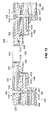
- FIG. 1 is a prior art diagram of a pad side of an integrated circuit package after conventional processing techniques have been used to form plating traces, form and electroplate pad areas on the pad side, and partially remove the plating traces;
- FIG. 2 is an exemplary diagram of the pad side of an integrated circuit package after processing techniques in accordance with exemplary embodiments of the present invention have been used to form and electroplate pad areas on the pad side;
- FIG. 3 is an exemplary block diagram of a panel having four integrated circuit packages formed in accordance with an exemplary embodiment of the present invention, where the panel is electrically coupled to a current source used for electroplating;
- FIG. 4 is an exemplary method for processing an integrated circuit package
- FIGS. 5 through 16 are exemplary cross-sectional views of an integrated circuit package used to illustrate process steps in accordance with an exemplary method of the present invention
- FIGS. 17 , 18 , and 19 show examples of a back plane view, a cross-sectional view, and a pad side view, respectively, of an integrated circuit package after electroplating has been performed, the back plane has been patterned, and a solder mask has been formed over the back plane;
- FIG. 20 shows an enlarged exemplary top view showing a back plane of the integrated circuit package of FIG. 17 .
- electroplating nickel and gold on integrated circuit packages requires plating traces for providing the connectivity to distribute current used during electroplating to the exposed pad areas to be plated.
- the plating traces are removed by etching to enhance the electrical performance of an integrated circuit residing in the integrated circuit package and operating at frequencies greater than approximately two GHz.
- the plating traces left untouched act as antennas that could cause functional errors in the IC packaged in the integrated circuit package. Nevertheless, even the process of removing the plating traces causes problems, as described below.
- etch away the plating traces requires large openings formed in a solder mask, itself formed over a surface of the pad side of the integrated circuit package.
- the plating traces typically comprised of copper, are first covered by a Dry Resist (DR) film during electroplating and then removed during etching of the copper plating traces within the solder mask openings.
- DR Dry Resist
- the openings in the solder mask also known as “etch back windows,” require fairly large areas to compensate for solder mask positional tolerances. Thus, these etch back windows cannot always fit on the outer surface of the pad side in a dense pattern, as is typically required for pad areas on the pad side. Moreover, a little portion of plating tail is still left because of the process tolerances, as shown in FIG. 1 .
- FIG. 1 shows an example of an outer surface 135 of the pad side 100 of an integrated circuit package after conventional processing has been performed to form plating traces 110 , form pad areas 155 , electroplate the solder mask defined pad areas 175 , and etch the plating traces.
- the integrated circuit package has been subjected to an electroplating process in order to plate pad areas 175 .
- Plating tails 110 are portions of plating traces that were unable to be removed due to processing tolerances.
- the plating tails 110 When operating speeds are less than approximately two GHz, the plating tails 110 typically do not pose a problem. However, as operating speeds increase, the plating tails 110 begin to act as antennas and can create functional errors in the IC (not shown in FIG. 1 ) to which the pad areas 155 are electrically coupled. Consequently, conventional processing of integrated circuit packages has problems with plating traces used for electroplating.
- Exemplary embodiments of the present invention solve the above problems by providing methods and apparatus made therefrom that do not have plating tails 110 on the pad side 100 of an integrated circuit package.
- FIG. 2 an example is shown of the pad side 100 of an integrated circuit package after techniques of the present invention have been used to form the integrated circuit package. Because exemplary embodiments of the present invention do not use plating traces on the outer surface 135 of the pad side 100 of an integrated circuit package, there are no plating tails 110 in FIG. 2 .
- Panel 300 is shown electrically coupled to a current source 310 used for electroplating.
- Panel 300 comprises, as an example, four integrated circuit packages 480 - 1 through 480 - 4 , although the panel 300 may contain any number of IC packages 480 .
- Panel 300 has a plating bar 320 that is used to electrically couple the four integrated circuit packages 480 - 1 through 480 - 4 during electroplating.
- Each integrated circuit package 480 has a back plane (described below in referenced FIGS. 5 through 19 ), which is electrically coupled to other integrated circuit packages 480 through the plating bar 320 .
- Plating bar 320 is electrically coupled to the current source 310 when electroplating is performed.
- Electroplating and processing of panels 300 is well known to those skilled in the art. However, exemplary embodiments of the present invention change the sequence of steps at which certain processing is performed and also how connections to the integrated circuit packages 480 for use during electroplating are made. These concepts are described in more detail below.
- an exemplary method 400 is shown for processing an integrated circuit package.
- FIGS. 5 to 19 show these steps in additional detail.
- the present invention can be used to electroplate integrated circuit packages, where the electroplating is performed without forming plating traces on a conductive surface of a pad side of the integrated circuit packages.
- Method 400 shows one example of techniques suitable for electroplating without forming plating traces on the pad side of the integrated circuit packages, and other techniques may also be used.
- the electroplating is used to plate a number of pad areas of the integrated circuit package with one or more materials.
- the materials are typically nickel followed by gold (e.g., copper pad areas are electroplated with nickel and then the nickel is electroplated with gold). However, any material or materials may be used.
- the back plane of the integrated circuit package is coupled to one or more current sources to be used during electroplating.
- the back plane is electrically coupled to the one or more current sources through backside edge traces, which are shown in more exemplary detail in FIG. 20 and are part of the back plane. Electrical coupling of the back plane is any coupling allowing current to flow through any part of the back plane.
- the backside edge traces are formed as part of the back plane.
- the back plane is electrically coupled to the one or more current sources, typically through a plating bar.
- the back plane Prior to electroplating (step 402 ), the back plane is left substantially unpatterned, except for the backside edge traces and plated through-holes.
- the substantially unpatterned back plane will be electrically coupled, during electroplating, so that current travels from the one or more current sources through the back plane (or some portion thereof) to the pad areas to be electroplated.
- the current passes through pad areas after passing through the back plane. In other words, the current passes through the back plane first then passes through each of the pad areas being electroplated.
- step 402 electroplating is performed using electroplating processes well known to those skilled in the art. Electroplating uses an appropriate plating bath and the one or more current sources. Electroplating will plate the pad areas with one or more materials. Typically, step 402 is performed twice, once to first plate the pad areas with nickel and then another time to plate the pad areas with gold. Each electroplating step 402 generally uses a separate plating bath in order to plate separate materials. Any type of materials may be used in step 402 that can be electroplated, and any number of materials and associated plating baths may be used.
- step 403 the back plane is patterned.
- the patterning of the back plane occurs after the step of electroplating (step 402 ), as the back plane is used to deliver current during the electroplating step (step 402 ) to the pad areas.
- the back plane is patterned (step 403 ) prior to electroplating (step 402 ).
- FIGS. 5 through 16 illustrate various method steps of an exemplary embodiment of the present invention.
- a cross-sectional view of an exemplary integrated circuit package 480 is shown.
- integrated circuit package 480 comprises a number of dielectric layers 520 , a number of copper layers 525 , a number of through-holes 420 , a cavity 425 , and a number of openings 550 in the copper layers 525 .
- openings 550 can be used to separate portions of internal or external copper layers 525 to create pad areas to be used for electrically coupling an IC to the integrated circuit package 480 .
- the integrated circuit package 480 has backside edge traces (not shown in FIG. 5 but shown in FIG. 20 ) to electrically couple the back plane 410 , on the backside of the integrated circuit package 480 , to the pad side 430 of the integrated circuit package 480 .
- the cavity 425 is used to package a high power dissipating IC (e.g., greater than approximately 3 watts), which will be electrically coupled to pad areas (shown in FIGS. 9–16 ) internal to the integrated circuit package 480 .
- a high power dissipating IC e.g., greater than approximately 3 watts
- pad areas shown in FIGS. 9–16
- integrated circuit packages processed in accordance with the present invention may be used to package any IC.
- the through-holes 420 have been drilled, plated with plating material 560 (e.g., copper) and filled with via plugging material 555 , as is known in the art.
- plating material 560 e.g., copper
- Internal copper layers have been patterned and laminated together, as is also known in the art. For instance, typically sheets having copper foil over dielectric 520 are used and are laminated together and plated with additional copper.
- a copper layer 525 can comprise a copper foil and additional copper layers added through techniques such as electroless plating and electroplating.
- the back plane 410 and pad layer 430 are substantially unpatterned. The back plane 410 is opposite the pad side 430 , where pad areas will be formed for connection to a circuit board.
- a Dry Film Resist (DFR) layer 610 has been applied over the back plane 410 and pad side 430 .
- the DFR layer 610 on the back plane 410 is left intact, but the DFR layer 610 on the pad layer 430 is imaged and developed to form openings 620 .
- the copper layer 525 of the pad layer 430 has been etched and the DFR layer 610 has been stripped. Openings 720 in the pad layer 430 correspond to openings 620 in the DFR layer 610 (see FIG. 7 ).
- FIG. 9 another DFR layer 910 has been formed on the back plane 410 , and a solder mask 920 has been formed and patterned on the pad layer 430 to form pad areas 930 . Additionally, FIG. 9 also shows pad areas 940 , formed internal to the integrated circuit package 480 . Pad areas 940 are formed during prior processing steps, when openings 550 are formed. Some of the openings 550 are used to create the pad areas 940 , which are used to electrically couple an IC (shown below) to the integrated circuit package.
- FIG. 10 shows the integrated circuit package 480 after electroplating has been performed.
- Any exposed conductive surface e.g., a copper surface
- the current source will be electroplated, thereby forming layer 1010 .
- nickel and gold have been applied to form layer 1010 .
- a layer of nickel will be electroplated onto the exposed copper pad areas 930 , 940 of the integrated circuit package 480
- a layer of gold will be electroplated onto the same exposed copper pad areas 930 , 940 of the integrated circuit package 480 .
- the layer 1010 therefore comprises two layers. However, more or less layers can be used and different materials may also be used.
- the pad areas 930 , 940 are now plated.
- the back plane 410 can be patterned, as the back plane 410 is no longer going to be used to electrically couple current from a current source (shown in FIG. 3 ) to the pad areas 930 of the pad layer 430 and the pad areas 940 .
- a current source shown in FIG. 3
- the DFR layer 910 is imaged and developed to form openings 1110 and the copper layers 525 are etched in FIG. 12 .
- gold plating in the layer 1010 acts as an etch resist.
- FIG. 13 the DFR layer on back plane 410 has been stripped.
- a solder mask 1410 has been formed on the back plane 410 .
- FIG. 15 a copper slug 1510 has been attached to the backside 410 , with an adhesive 1520 .
- FIG. 16 shows an integrated circuit package 480 after an integrated circuit 1620 has been placed in cavity 425 .
- Integrated circuit package 480 therefore comprises an integrated circuit 1620 electrically coupled to areas 1010 through wire bonds 1640 . Additionally, solder balls 1610 have been added and electrically coupled to the layers 1010 of pad areas 930 .
- FIGS. 17 , 18 , and 19 show examples of a back plane 410 view, a cross-sectional view, and a pad side 430 view, respectively, of an integrated circuit package after electroplating has been performed, the back plane 410 has been patterned, and a solder mask 1410 has been formed over the back plane 410 .
- FIG. 17 a view is shown of the back plane 410 of the integrated circuit package 480 .
- Back plane 410 is shown after solder mask 1410 has been applied to the integrated circuit package 480 (see FIG. 14 ).
- FIG. 18 shows a cross-sectional view of the integrated circuit package 480 .
- FIG. 18 shows a patterned copper layer 525 for back plane 410 , where openings 1810 have been made in copper layer 525 .
- FIG. 19 is a view of the pad side 430 of the integrated circuit package 480 .
- the solder mask layer 920 has been patterned to reveal pad areas 930 , which have been plated.
- FIG. 20 is an enlarged view of the back plane 410 of the integrated circuit package 480 .
- Through-holes 420 are shown.
- backside edge traces 490 are integral to the back plane 410 and are formed at the edge of the integrated circuit package 480 .
- these backside edge traces 490 will be electrically coupled to the plating bar 350 (see FIG. 3 ) during electroplating, as described in an exemplary embodiment above.
Landscapes
- Engineering & Computer Science (AREA)
- Physics & Mathematics (AREA)
- Microelectronics & Electronic Packaging (AREA)
- Condensed Matter Physics & Semiconductors (AREA)
- General Physics & Mathematics (AREA)
- Computer Hardware Design (AREA)
- Power Engineering (AREA)
- Manufacturing & Machinery (AREA)
- Geometry (AREA)
- Ceramic Engineering (AREA)
- Electroplating Methods And Accessories (AREA)
Priority Applications (3)
| Application Number | Priority Date | Filing Date | Title |
|---|---|---|---|
| US10/878,157 US7157361B2 (en) | 2004-06-28 | 2004-06-28 | Methods for processing integrated circuit packages formed using electroplating and apparatus made therefrom |
| KR1020050055694A KR101421714B1 (ko) | 2004-06-28 | 2005-06-27 | 집적 회로 패키지 처리 방법 및 집적 회로 패키지 |
| JP2005188120A JP5676833B2 (ja) | 2004-06-28 | 2005-06-28 | 電気めっきを使用して形成される集積回路パッケージを処理するための方法およびそれから作成された装置 |
Applications Claiming Priority (1)
| Application Number | Priority Date | Filing Date | Title |
|---|---|---|---|
| US10/878,157 US7157361B2 (en) | 2004-06-28 | 2004-06-28 | Methods for processing integrated circuit packages formed using electroplating and apparatus made therefrom |
Publications (2)
| Publication Number | Publication Date |
|---|---|
| US20060014370A1 US20060014370A1 (en) | 2006-01-19 |
| US7157361B2 true US7157361B2 (en) | 2007-01-02 |
Family
ID=35600011
Family Applications (1)
| Application Number | Title | Priority Date | Filing Date |
|---|---|---|---|
| US10/878,157 Active 2025-01-26 US7157361B2 (en) | 2004-06-28 | 2004-06-28 | Methods for processing integrated circuit packages formed using electroplating and apparatus made therefrom |
Country Status (3)
| Country | Link |
|---|---|
| US (1) | US7157361B2 (ko) |
| JP (1) | JP5676833B2 (ko) |
| KR (1) | KR101421714B1 (ko) |
Families Citing this family (3)
| Publication number | Priority date | Publication date | Assignee | Title |
|---|---|---|---|---|
| JP6152254B2 (ja) * | 2012-09-12 | 2017-06-21 | 新光電気工業株式会社 | 半導体パッケージ、半導体装置及び半導体パッケージの製造方法 |
| KR20140108865A (ko) * | 2013-03-04 | 2014-09-15 | 삼성전자주식회사 | 패키지 기판, 패키지 기판의 제조 방법 및 패키지 기판을 포함하는 반도체 패키지 |
| CN111246669B (zh) * | 2020-01-17 | 2021-07-30 | 深圳市德明利技术股份有限公司 | 一种lpddr基板设计方法、lpddr基板和电子设备 |
Citations (2)
| Publication number | Priority date | Publication date | Assignee | Title |
|---|---|---|---|---|
| US6566166B2 (en) * | 2000-04-14 | 2003-05-20 | Via Technologies Inc. | Method of manufacturing a cavity-down plastic ball grid array (CD-PBGA) substrate |
| US6569712B2 (en) * | 2001-10-19 | 2003-05-27 | Via Technologies, Inc. | Structure of a ball-grid array package substrate and processes for producing thereof |
Family Cites Families (2)
| Publication number | Priority date | Publication date | Assignee | Title |
|---|---|---|---|---|
| JP3339473B2 (ja) * | 1999-08-26 | 2002-10-28 | 日本電気株式会社 | パッケージ基板、該パッケージ基板を備える半導体装置及びそれらの製造方法 |
| JP2001068828A (ja) * | 1999-08-27 | 2001-03-16 | Ngk Spark Plug Co Ltd | 配線基板及びその製造方法 |
-
2004
- 2004-06-28 US US10/878,157 patent/US7157361B2/en active Active
-
2005
- 2005-06-27 KR KR1020050055694A patent/KR101421714B1/ko active IP Right Grant
- 2005-06-28 JP JP2005188120A patent/JP5676833B2/ja active Active
Patent Citations (2)
| Publication number | Priority date | Publication date | Assignee | Title |
|---|---|---|---|---|
| US6566166B2 (en) * | 2000-04-14 | 2003-05-20 | Via Technologies Inc. | Method of manufacturing a cavity-down plastic ball grid array (CD-PBGA) substrate |
| US6569712B2 (en) * | 2001-10-19 | 2003-05-27 | Via Technologies, Inc. | Structure of a ball-grid array package substrate and processes for producing thereof |
Also Published As
| Publication number | Publication date |
|---|---|
| KR101421714B1 (ko) | 2014-08-13 |
| JP5676833B2 (ja) | 2015-02-25 |
| JP2006013519A (ja) | 2006-01-12 |
| US20060014370A1 (en) | 2006-01-19 |
| KR20060048554A (ko) | 2006-05-18 |
Similar Documents
| Publication | Publication Date | Title |
|---|---|---|
| JP4248761B2 (ja) | 半導体パッケージ及びその製造方法並びに半導体装置 | |
| US7622377B2 (en) | Microfeature workpiece substrates having through-substrate vias, and associated methods of formation | |
| JP3895303B2 (ja) | メッキリード線を使用しないパッケージ基板の製造方法 | |
| KR100395862B1 (ko) | 플립 칩형 반도체 장치 및 플립 칩형 반도체 장치 제조 방법 | |
| KR100499003B1 (ko) | 도금 인입선을 사용하지 않는 패키지 기판 및 그 제조 방법 | |
| US8633587B2 (en) | Package structure | |
| US6569712B2 (en) | Structure of a ball-grid array package substrate and processes for producing thereof | |
| KR20040076164A (ko) | 도금 인입선을 사용하지 않는 패키지 기판 및 그 제조 방법 | |
| JP2004221583A (ja) | 平衡積層構造(balancedlamination)を利用したフレックス(flex)・ベースのICパッケージ構造 | |
| US20030014863A1 (en) | Method for manufacturing a printed circuit board | |
| US8043514B2 (en) | Method of manufacturing a wiring board by utilizing electro plating | |
| KR101421714B1 (ko) | 집적 회로 패키지 처리 방법 및 집적 회로 패키지 | |
| US9060430B1 (en) | Shielded trace structure and fabrication method | |
| US6207354B1 (en) | Method of making an organic chip carrier package | |
| KR100693168B1 (ko) | 인쇄회로기판 및 그 제조방법 | |
| US7061084B2 (en) | Lead-bond type chip package and manufacturing method thereof | |
| KR20040076165A (ko) | 도금 인입선을 사용하지 않는 패키지 기판 및 그 제조 방법 | |
| JPH08316360A (ja) | Ic実装構造 | |
| KR20090016257A (ko) | 도금 인입선이 제거된 패키지 기판 및 그 제조 방법 | |
| JP3831173B2 (ja) | 半導体モジュール | |
| KR20030072855A (ko) | 플립칩 비지에이 반도체 패키지용 인쇄회로기판의범프패드 도금방법 | |
| JP2006294825A (ja) | 半導体集積回路装置 | |
| KR20040110531A (ko) | 도금 인입선이 단축된 패키지 기판 및 그 제조방법 | |
| JPH09246416A (ja) | 半導体装置 | |
| KR20010005136A (ko) | 패키지 기판 제조방법 |
Legal Events
| Date | Code | Title | Description |
|---|---|---|---|
| AS | Assignment |
Owner name: AGERE SYSTEMS INC., PENNSYLVANIA Free format text: ASSIGNMENT OF ASSIGNORS INTEREST;ASSIGNORS:CHOWDHURY, MUSAWIR;COHN, CHARLES;REEL/FRAME:015556/0592 Effective date: 20040628 |
|
| STCF | Information on status: patent grant |
Free format text: PATENTED CASE |
|
| FPAY | Fee payment |
Year of fee payment: 4 |
|
| FPAY | Fee payment |
Year of fee payment: 8 |
|
| AS | Assignment |
Owner name: AVAGO TECHNOLOGIES GENERAL IP (SINGAPORE) PTE. LTD Free format text: ASSIGNMENT OF ASSIGNORS INTEREST;ASSIGNOR:AGERE SYSTEMS LLC;REEL/FRAME:035365/0634 Effective date: 20140804 |
|
| AS | Assignment |
Owner name: BANK OF AMERICA, N.A., AS COLLATERAL AGENT, NORTH CAROLINA Free format text: PATENT SECURITY AGREEMENT;ASSIGNOR:AVAGO TECHNOLOGIES GENERAL IP (SINGAPORE) PTE. LTD.;REEL/FRAME:037808/0001 Effective date: 20160201 Owner name: BANK OF AMERICA, N.A., AS COLLATERAL AGENT, NORTH Free format text: PATENT SECURITY AGREEMENT;ASSIGNOR:AVAGO TECHNOLOGIES GENERAL IP (SINGAPORE) PTE. LTD.;REEL/FRAME:037808/0001 Effective date: 20160201 |
|
| AS | Assignment |
Owner name: AVAGO TECHNOLOGIES GENERAL IP (SINGAPORE) PTE. LTD., SINGAPORE Free format text: TERMINATION AND RELEASE OF SECURITY INTEREST IN PATENTS;ASSIGNOR:BANK OF AMERICA, N.A., AS COLLATERAL AGENT;REEL/FRAME:041710/0001 Effective date: 20170119 Owner name: AVAGO TECHNOLOGIES GENERAL IP (SINGAPORE) PTE. LTD Free format text: TERMINATION AND RELEASE OF SECURITY INTEREST IN PATENTS;ASSIGNOR:BANK OF AMERICA, N.A., AS COLLATERAL AGENT;REEL/FRAME:041710/0001 Effective date: 20170119 |
|
| AS | Assignment |
Owner name: BELL SEMICONDUCTOR, LLC, ILLINOIS Free format text: ASSIGNMENT OF ASSIGNORS INTEREST;ASSIGNORS:AVAGO TECHNOLOGIES GENERAL IP (SINGAPORE) PTE. LTD.;BROADCOM CORPORATION;REEL/FRAME:044886/0766 Effective date: 20171208 |
|
| AS | Assignment |
Owner name: CORTLAND CAPITAL MARKET SERVICES LLC, AS COLLATERA Free format text: SECURITY INTEREST;ASSIGNORS:HILCO PATENT ACQUISITION 56, LLC;BELL SEMICONDUCTOR, LLC;BELL NORTHERN RESEARCH, LLC;REEL/FRAME:045216/0020 Effective date: 20180124 |
|
| MAFP | Maintenance fee payment |
Free format text: PAYMENT OF MAINTENANCE FEE, 12TH YEAR, LARGE ENTITY (ORIGINAL EVENT CODE: M1553) Year of fee payment: 12 |
|
| AS | Assignment |
Owner name: BELL NORTHERN RESEARCH, LLC, ILLINOIS Free format text: RELEASE BY SECURED PARTY;ASSIGNOR:CORTLAND CAPITAL MARKET SERVICES LLC;REEL/FRAME:059723/0382 Effective date: 20220401 Owner name: BELL SEMICONDUCTOR, LLC, ILLINOIS Free format text: RELEASE BY SECURED PARTY;ASSIGNOR:CORTLAND CAPITAL MARKET SERVICES LLC;REEL/FRAME:059723/0382 Effective date: 20220401 Owner name: HILCO PATENT ACQUISITION 56, LLC, ILLINOIS Free format text: RELEASE BY SECURED PARTY;ASSIGNOR:CORTLAND CAPITAL MARKET SERVICES LLC;REEL/FRAME:059723/0382 Effective date: 20220401 |