US7136085B2 - Image-forming apparatus and optical scanner - Google Patents
Image-forming apparatus and optical scanner Download PDFInfo
- Publication number
- US7136085B2 US7136085B2 US10/882,222 US88222204A US7136085B2 US 7136085 B2 US7136085 B2 US 7136085B2 US 88222204 A US88222204 A US 88222204A US 7136085 B2 US7136085 B2 US 7136085B2
- Authority
- US
- United States
- Prior art keywords
- image
- scanning direction
- pixel clock
- clock signal
- phase
- Prior art date
- Legal status (The legal status is an assumption and is not a legal conclusion. Google has not performed a legal analysis and makes no representation as to the accuracy of the status listed.)
- Active, expires
Links
Images


Classifications
-
- H—ELECTRICITY
- H04—ELECTRIC COMMUNICATION TECHNIQUE
- H04N—PICTORIAL COMMUNICATION, e.g. TELEVISION
- H04N1/00—Scanning, transmission or reproduction of documents or the like, e.g. facsimile transmission; Details thereof
- H04N1/04—Scanning arrangements, i.e. arrangements for the displacement of active reading or reproducing elements relative to the original or reproducing medium, or vice versa
- H04N1/047—Detection, control or error compensation of scanning velocity or position
- H04N1/053—Detection, control or error compensation of scanning velocity or position in main scanning direction, e.g. synchronisation of line start or picture elements in a line
-
- H—ELECTRICITY
- H04—ELECTRIC COMMUNICATION TECHNIQUE
- H04N—PICTORIAL COMMUNICATION, e.g. TELEVISION
- H04N1/00—Scanning, transmission or reproduction of documents or the like, e.g. facsimile transmission; Details thereof
- H04N1/04—Scanning arrangements, i.e. arrangements for the displacement of active reading or reproducing elements relative to the original or reproducing medium, or vice versa
- H04N1/113—Scanning arrangements, i.e. arrangements for the displacement of active reading or reproducing elements relative to the original or reproducing medium, or vice versa using oscillating or rotating mirrors
- H04N1/1135—Scanning arrangements, i.e. arrangements for the displacement of active reading or reproducing elements relative to the original or reproducing medium, or vice versa using oscillating or rotating mirrors for the main-scan only
-
- H—ELECTRICITY
- H04—ELECTRIC COMMUNICATION TECHNIQUE
- H04N—PICTORIAL COMMUNICATION, e.g. TELEVISION
- H04N1/00—Scanning, transmission or reproduction of documents or the like, e.g. facsimile transmission; Details thereof
- H04N1/04—Scanning arrangements, i.e. arrangements for the displacement of active reading or reproducing elements relative to the original or reproducing medium, or vice versa
- H04N1/12—Scanning arrangements, i.e. arrangements for the displacement of active reading or reproducing elements relative to the original or reproducing medium, or vice versa using the sheet-feed movement or the medium-advance or the drum-rotation movement as the slow scanning component, e.g. arrangements for the main-scanning
-
- H—ELECTRICITY
- H04—ELECTRIC COMMUNICATION TECHNIQUE
- H04N—PICTORIAL COMMUNICATION, e.g. TELEVISION
- H04N2201/00—Indexing scheme relating to scanning, transmission or reproduction of documents or the like, and to details thereof
- H04N2201/04—Scanning arrangements
- H04N2201/047—Detection, control or error compensation of scanning velocity or position
- H04N2201/04701—Detection of scanning velocity or position
- H04N2201/0471—Detection of scanning velocity or position using dedicated detectors
- H04N2201/04713—Details of the detector arrangement, e.g. non-standard position, optical details
-
- H—ELECTRICITY
- H04—ELECTRIC COMMUNICATION TECHNIQUE
- H04N—PICTORIAL COMMUNICATION, e.g. TELEVISION
- H04N2201/00—Indexing scheme relating to scanning, transmission or reproduction of documents or the like, and to details thereof
- H04N2201/04—Scanning arrangements
- H04N2201/047—Detection, control or error compensation of scanning velocity or position
- H04N2201/04701—Detection of scanning velocity or position
- H04N2201/04715—Detection of scanning velocity or position by detecting marks or the like, e.g. slits
- H04N2201/04722—Detection of scanning velocity or position by detecting marks or the like, e.g. slits on a photoconductive drum or belt
-
- H—ELECTRICITY
- H04—ELECTRIC COMMUNICATION TECHNIQUE
- H04N—PICTORIAL COMMUNICATION, e.g. TELEVISION
- H04N2201/00—Indexing scheme relating to scanning, transmission or reproduction of documents or the like, and to details thereof
- H04N2201/04—Scanning arrangements
- H04N2201/047—Detection, control or error compensation of scanning velocity or position
- H04N2201/04701—Detection of scanning velocity or position
- H04N2201/04732—Detecting at infrequent intervals, e.g. once or twice per line for main-scan control
-
- H—ELECTRICITY
- H04—ELECTRIC COMMUNICATION TECHNIQUE
- H04N—PICTORIAL COMMUNICATION, e.g. TELEVISION
- H04N2201/00—Indexing scheme relating to scanning, transmission or reproduction of documents or the like, and to details thereof
- H04N2201/04—Scanning arrangements
- H04N2201/047—Detection, control or error compensation of scanning velocity or position
- H04N2201/04701—Detection of scanning velocity or position
- H04N2201/04734—Detecting at frequent intervals, e.g. once per line for sub-scan control
-
- H—ELECTRICITY
- H04—ELECTRIC COMMUNICATION TECHNIQUE
- H04N—PICTORIAL COMMUNICATION, e.g. TELEVISION
- H04N2201/00—Indexing scheme relating to scanning, transmission or reproduction of documents or the like, and to details thereof
- H04N2201/04—Scanning arrangements
- H04N2201/047—Detection, control or error compensation of scanning velocity or position
- H04N2201/04701—Detection of scanning velocity or position
- H04N2201/04744—Detection of scanning velocity or position by detecting the scanned beam or a reference beam
-
- H—ELECTRICITY
- H04—ELECTRIC COMMUNICATION TECHNIQUE
- H04N—PICTORIAL COMMUNICATION, e.g. TELEVISION
- H04N2201/00—Indexing scheme relating to scanning, transmission or reproduction of documents or the like, and to details thereof
- H04N2201/04—Scanning arrangements
- H04N2201/047—Detection, control or error compensation of scanning velocity or position
- H04N2201/04701—Detection of scanning velocity or position
- H04N2201/04749—Detecting position relative to a gradient, e.g. using triangular-shaped masks, marks or gratings
-
- H—ELECTRICITY
- H04—ELECTRIC COMMUNICATION TECHNIQUE
- H04N—PICTORIAL COMMUNICATION, e.g. TELEVISION
- H04N2201/00—Indexing scheme relating to scanning, transmission or reproduction of documents or the like, and to details thereof
- H04N2201/04—Scanning arrangements
- H04N2201/047—Detection, control or error compensation of scanning velocity or position
- H04N2201/04753—Control or error compensation of scanning position or velocity
- H04N2201/04758—Control or error compensation of scanning position or velocity by controlling the position of the scanned image area
- H04N2201/04767—Control or error compensation of scanning position or velocity by controlling the position of the scanned image area by controlling the timing of the signals, e.g. by controlling the frequency o phase of the pixel clock
- H04N2201/04781—Controlling the phase of the signals
-
- H—ELECTRICITY
- H04—ELECTRIC COMMUNICATION TECHNIQUE
- H04N—PICTORIAL COMMUNICATION, e.g. TELEVISION
- H04N2201/00—Indexing scheme relating to scanning, transmission or reproduction of documents or the like, and to details thereof
- H04N2201/04—Scanning arrangements
- H04N2201/047—Detection, control or error compensation of scanning velocity or position
- H04N2201/04753—Control or error compensation of scanning position or velocity
- H04N2201/04793—Control or error compensation of scanning position or velocity using stored control or compensation data, e.g. previously measured data
Definitions
- the present invention relates generally to image-forming apparatuses and optical scanners, and more particularly to an image-forming apparatus and an optical scanner that employ an LD (laser diode) optical system.
- LD laser diode
- Some conventional image-forming apparatuses employ a laser beam to form an image.
- the image-forming apparatuses form an image by an optical scanner emitting a laser beam on the scanning surface (or the surface to be scanned) of a photosensitive body (a medium to be scanned).
- FIG. 1 is a diagram showing an image-forming operation by a conventional image-forming apparatus employing the laser-beam method.
- a charging unit such as a roller-type contact charger evenly charges a photosensitive body.
- a laser light source 1101 emits a laser beam to a rotary polygon mirror 1103 .
- the polygon mirror 1103 periodically deflects the laser beam emitted from the laser light source 1101 so that the laser beam is transmitted through an f ⁇ lens 1105 to scan the scanning surface of the photosensitive body repeatedly along a main scanning direction, the photosensitive body moving (rotating) in a sub scanning direction.
- static electricity is removed from a beam spot or a part onto which the laser beam is emitted, so that an electrostatic pattern (an electrostatic latent image) is formed on the photosensitive body.
- a controller causes image data in units of pages to be fed line by line (scan by scan) as an image signal (a video signal) to a laser driving circuit.
- the laser driving circuit outputs the image signal to the laser light source 1101 in synchronization with a pixel clock signal (a writing clock signal) to perform modulation.
- the pixel clock signal is input via a phase synchronization circuit from a pixel clock generator circuit (not graphically represented) forming a pixel clock generation part and a phase setting part.
- FIG. 2 is a timing chart showing an example of the relationship between the pixel clock signal and its phase change.
- the pixel clock generator circuit establishes synchronization with a synchronization detection signal input from a synchronization detection sensor, and generates and outputs a pixel clock signal clkw of (b), using a reference clock signal (an original clock signal) clko of (a) n times (four times in FIG.
- the reference clock signal clko is generated from an oscillator not graphically represented.
- the optical scanner When the above-described optical scanner writes the electrostatic latent image by forming laser beam spots on the scanning surface, the optical scanner performs control so that the laser beam spots are written or formed at a uniform density.
- the f ⁇ lens 1105 undergoes distortion so that its refractive index is changed. Further, when an environmental variation such as a change in temperature occurs around the laser light source 1101 , the wavelength of the laser beam emitted from the laser light source is changed. The f ⁇ lens 1105 refracts the entering laser beam at a predetermined angle in accordance with the wavelength of the entering laser beam. As a result, as shown in FIG.
- an error may be caused in the angle of refraction of the laser beam entering the f ⁇ lens 1105 so as to cause an error in the writing magnification (optical scanning length) per main scanning period (hereinafter, scanning period) of the laser beam deflected by the polygon mirror 1103 , thus affecting an output image.
- the phase of the pixel clock signal clkw is shifted by phase changing to correct the writing magnification of the laser beam.
- the pixel clock generator circuit performs phase control using external pulse trains xpls in order to perform phase changing to shift the phase of the pixel clock signal clkw.
- an external pulse train xplsp for delaying the phase of the pixel clock signal clkw (indicated by (c) in FIG. 2 ) and an external pulse train xplsm for advancing the phase of the pixel clock signal clkw (indicated by (d) in FIG. 2 ).
- the external pulse train xplsp or xplsm is input to increase or decrease the number of pulses to be counted of the reference clock signal clko so that a pulse of the pixel clock signal clkw, which is normally generated at an interval of eight pulses of the reference clock signal clko, is generated at an interval of nine or seven pulses of the reference clock signal clko.
- the frequency of the pixel clock signal clkw is multiplied by 8/7 (advancing control) or 8/9 (delaying control).
- the frequency of the pixel clock signal clkw is multiplied by 8/7 (advancing control) or 8/9 (delaying control).
- Letting the time of one main scanning line be Tm this results in Tm ⁇ 7/8 (advancing control) (indicated by (f) in FIG. 2 ) or Tm+9/8 (delaying control) (indicated by (e) in FIG. 2 ).
- Tm ⁇ 7/8 (advancing control) indicated by (f) in FIG. 2
- Tm+9/8 delaying control
- the pixel clock generator circuit includes a pulse generator circuit generating the external pulse trains xplsp and xplsm.
- the pulse generator circuit generates the external pulse train (hereinafter also referred to simply as pulses) xplsp or xplsm in accordance with a portion of the pixel clock pulse (train) clkw on which portion it is desired to perform phase changing.
- FIG. 3 is a diagram showing a conventional pulse generator circuit.
- the pulse generator circuit includes comparators 1001 and 1002 and counters 1003 and 1004 .
- an engine CPU (not graphically represented) sets a pulse generation interval (period) prd in the comparator 1001 , and sets the number of pulses num in the comparator 1002 .
- the pulse generator circuit operates as follows when the laser beam is deflected by the polygon mirror 1103 to perform a scan in the main scanning direction.
- the counter 1003 When a clear signal xlclr generated from the synchronization detection signal by a circuit (not graphically represented) is input to the counter 1003 , the counter 1003 , using the inputting as a reference point, starts a counting operation to count the number of pulses of the pixel clock signal clkw (a count value i), and stops the counting operation when a stop signal is input to the counter 1003 from the comparator 1002 .
- the comparator 1001 compares the count value i of the counter 1003 and the preset pulse generation interval (hereinafter also referred to as a set value) prd, and generates a pulse (xpls) every time the count value i reaches the set value prd.
- the counter 1004 counts the number of pulses xpls generated from the comparator 1001 (a count value j).
- the comparator 1002 compares the count value j of the counter 1004 and the preset number of pulses (hereinafter also referred to as a set value) num, and generates the stop signal when the count value j reaches the set value num.
- FIG. 4 is a flowchart of the operation of the pulse generator circuit of FIG. 3 .
- step S 1001 when the pulse generator circuit is turned on, the counters 1003 and 1004 reset their respective count values i and j each to “1.”
- step S 1002 it is determined whether the clear signal xlclr has been input to the counter 1003 .
- the counter 1003 waits until the clear signal xlclr is input thereto.
- the counter 1003 increments the count value i by one every time a pulse of the pixel clock signal clkw is input thereto.
- step S 1004 the comparator 1001 compares the count value i and the set value prd, and determines whether the count value i has reached the set value prd. If the count value i has not reached the set value prd (that is, “NO” in step S 1004 ), the counter 1003 increments the count value i by one. The counter 1003 repeats the operation of step S 1003 until the count value i reaches the set value prd.
- step S 1005 the comparator 1001 outputs a pulse (xpls).
- the generated pulse xpls is input to the counter 1003 so that the count value i of the counter 1003 is reset to “1.”
- step S 1006 the comparator 1002 compares the count value j of the counter 1004 and the set value num, and determines whether the count value j of the counter 1004 has reached the set value num. If the count value j has not reached the set value num (that is, “NO” in step S 1006 ), in step S 1007 , the counter 1004 increments the count value j by one when the pulse xpls is input thereto.
- the counters 1003 and 1004 and the comparator 1001 repeat the above-described operations.
- the comparator 1002 generates the stop signal.
- the pulse generator circuit ends the above-described series of operations, which are hereinafter referred to as a pulse generation operation.
- FIG. 5 is a timing chart showing the conventional relationship between the clear signal xlclr and the external pulse train xpls.
- a pulse train generation part starts to output the external pulse train xpls indicated by (b) after the set value prd passes since the inputting of the clear signal xlclr indicated by (a). At this point, the pulse train generation part outputs as many pulses of a pulse width of one clock pulse clkw of the external pulse train xpls as the number of pulses num at the periods (intervals) prd before the inputting of the next clear signal xlclr.
- a fixed pulse train may be generated from output data obtained by counting up addresses based on a pixel clock signal.
- FIG. 6 is a diagram showing the conventional image-forming apparatus with no f ⁇ lens.
- the optical system performs scanning with the laser beam being deflected by the polygon mirror 1103 at equal angles, that is, in a way to draw an arc. Accordingly, when scanning is performed linearly for a line on the photosensitive body surface, the light beam forms beam spots (images) on the photosensitive body surface at varying intervals even if the same interval is assumed for the center and the ends of the line. Further, the distance of beam emission to the photosensitive body surface varies between the center and the ends of the line. As a result, the beam diameter also varies between the center and the ends of the line during the single scan on the photosensitive body surface.
- the image-forming apparatus of FIG. 1 includes the f ⁇ lens 1105 (and another lens group) in order to control the variations in beam spot interval and beam diameter caused in the image-forming apparatus of FIG. 6 .
- the refractive index is controlled so as to absorb the difference in magnification between the center and each end of a single scanning line on the photosensitive body.
- JP 2000-141754 in an image-forming apparatus where a light source is driven according to an image signal based on a writing clock signal, a scanning part causes a light beam emitted from the light source to perform scanning in the main scanning direction on a photosensitive body moving in the sub scanning direction so that an image is written on the photosensitive body, and the image on the photosensitive body is transferred onto transfer paper, the magnification of the image in the main scanning direction is corrected based on the size of the transfer paper in the main scanning direction.
- an optical beam scanner divides a scanning region on a scanning surface in two in the main scanning direction, and performs scanning with two imaging optical systems.
- FIG. 7 is a graph showing beam emission positions on a photosensitive body surface and magnification deviations according to a conventional image-forming apparatus using an f ⁇ lens as shown in FIG. 1 .
- the characteristic of the f ⁇ lens is corrected on average.
- magnification there is a tendency for magnification to become positive (+) within a predetermined distance from each end toward a center and negative ( ⁇ ) in the vicinity of the center and each end on a single scanning line.
- a more specific object of the present invention is to provide an image-forming apparatus that can eliminate the color misregistration and magnification deviations of an image in the main scanning direction by measuring partial magnifications and performing magnification correction in each region on a single scanning line with respect to each optical system provided in the image-forming apparatus.
- Another more specific object of the present invention is to provide an optical scanner suitable for such image forming.
- an image-forming apparatus including: at least one imaging optical system configured to form an electrostatic latent image on an evenly charged scanning surface of a medium to be scanned moving in a sub scanning direction by scanning the scanning surface in a main scanning direction perpendicular to the sub scanning direction by periodically deflecting a laser beam emitted from a laser light source with a rotary deflector; a pixel clock generation part configured to generate a pixel clock signal for controlling timing of emission of the laser beam by the laser light source and change a phase of the pixel clock signal; a region setting part configured to set length of each of a plurality of regions in the main scanning direction based on image writing magnifications in a line in the main scanning direction, the regions being formed by dividing part of the scanning surface corresponding to the line in the main scanning direction; and a phase control part configured to control the changing of the phase of the pixel clock signal region by region based on the image writing magnifications, wherein the formed image is transferred to a
- an image-forming apparatus including: at least one imaging optical system configured to form an electrostatic latent image on an evenly charged scanning surface of a medium to be scanned moving in a sub scanning direction by scanning the scanning surface in a main scanning direction perpendicular to the sub scanning direction by periodically deflecting a laser beam emitted from a laser light source with a rotary deflector; a print-out part configured to transfer the formed image to a transfer medium and print out the image; a pixel clock generation part configured to generate a pixel clock signal for controlling timing of emission of the laser beam by the laser light source and change a phase of the pixel clock signal; a region setting part configured to set length of each of a plurality of regions in the main scanning direction based on image writing magnifications in a line in the main scanning direction, the regions being formed by dividing part of the scanning surface corresponding to the line in the main scanning direction; and a phase control part configured to control the changing of the phase of the pixel clock signal region
- an image-forming apparatus including: at least one imaging optical system configured to form an electrostatic latent image on an evenly charged scanning surface of a medium to be scanned moving in a sub scanning direction by scanning the scanning surface in a main scanning direction perpendicular to the sub scanning direction by periodically deflecting a laser beam emitted from a laser light source with a rotary deflector; a print-out part configured to transfer the formed image to a transfer medium and print out the image; a pixel clock generation part configured to generate a pixel clock signal for controlling timing of emission of the laser beam by the laser light source and change a phase of the pixel clock signal; a region setting part configured to set length of each of a plurality of regions in the main scanning direction based on image writing magnifications in a line in the main scanning direction, the regions being formed by dividing part of the scanning surface corresponding to the line in the main scanning direction; a reading part configured to read the printed-out image; and a phase control part configured
- an optical scanner for forming an electrostatic latent image on an evenly charged scanning surface of a medium to be scanned moving in a sub scanning direction by scanning the scanning surface in a main scanning direction perpendicular to the sub scanning direction by periodically deflecting a laser beam emitted from a laser light source with a rotary deflector
- the optical scanner including: a pixel clock generation part configured to generate a pixel clock signal for controlling timing of emission of the laser beam by the laser light source and change a phase of the pixel clock signal with respect to each of a plurality of regions on the scanning surface, the regions each having length thereof in the main scanning direction set based on image writing magnifications in a line in the main scanning direction.
- image writing magnification may be measured for each of divided regions in the main scanning direction and the image writing magnification may be corrected region by region. Accordingly, it is possible to eliminate the color misregistration and magnification deviations of an image in the main scanning direction. Further, according to the present invention, it is possible to realize an optical system in which distortion in the main scanning direction after f ⁇ correction is controlled and that has an optimum characteristic adapted to each optical unit.
- FIG. 1 is a diagram showing an image-forming operation by a conventional image-forming apparatus employing a laser-beam method
- FIG. 2 is a timing chart showing an example of the conventional relationship between a pixel clock signal and its phase change
- FIG. 3 is a diagram showing a conventional pulse generator circuit
- FIG. 4 is a flowchart of the operation of the conventional pulse generator circuit
- FIG. 5 is a timing chart showing the conventional relationship between a clear signal and an external pulse train
- FIG. 6 is a diagram showing the conventional image-forming apparatus with no f ⁇ lens
- FIG. 7 is a graph showing beam emission positions on a photosensitive body surface and magnification deviations according to a conventional image-forming apparatus
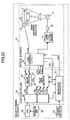
- FIG. 8 is a block diagram showing an image-forming apparatus according to a first embodiment of the present invention.
- FIG. 9 is a block diagram showing more detailed configurations of a pulse train generator part and a region generator part according to the first embodiment of the present invention.
- FIG. 10 is a block diagram showing a configuration of each of pulse generator circuits according to the first embodiment of the present invention.
- FIG. 11 is a flowchart of the operation of generating pulses by the pulse train generator part according to the first embodiment of the present invention.
- FIG. 12 is a flowchart of a pulse generation operation by each of the pulse generator circuits according to the first embodiment of the present invention.
- FIG. 13 is a diagram showing an external pulse train output from the pulse train generator part according to the first embodiment of the present invention.
- FIG. 14 is a schematic diagram showing an optical system unit and a unit measurement device according to the first embodiment of the present invention.
- FIG. 15 is a timing chart of signals at the time of correcting writing magnification according to the first embodiment of the present invention.
- FIG. 16A is a diagram showing a position sensor
- FIG. 16B is a graph showing signals output from the position sensor
- FIG. 16C is a graph showing output signals in the case of using a charge-coupled device according to the first embodiment of the present invention
- FIG. 17 is a graph showing writing magnification deviations in the position sensors calculated based on the light receiving positions thereof according to the first embodiment of the present invention.
- FIG. 18 is a block diagram showing the unit measurement device according to the first embodiment of the present invention.
- FIG. 19 is a table of corrections of image writing magnification in a main scanning direction and correction coefficients according to the first embodiment of the present invention.
- FIG. 20 is a diagram showing a photosensitive body and position detection sensors according to the first embodiment of the present invention.
- FIG. 21 is a diagram showing a method of detecting a detection pattern by the position detection sensors according to the first embodiment of the present invention.
- FIG. 22 is a flowchart of error detection by the image-forming apparatus according to the first embodiment of the present invention.
- FIG. 23 is a block diagram showing an image-forming apparatus according to a second embodiment of the present invention.
- FIG. 24 is a block diagram showing an image-forming apparatus according to a third embodiment of the present invention.
- FIG. 25 is a block diagram showing more detailed configurations of the pulse train generator part and the region generator part according to the third embodiment of the present invention.
- FIG. 26 is a block diagram showing a configuration of each of pulse generator circuits according to the third embodiment of the present invention.
- FIG. 27 is a flowchart of the operation of generating pulses by the pulse train generator part according to the third embodiment of the present invention.
- FIG. 28 is a flowchart of a pulse generation operation by each of the pulse generator circuits according to the third embodiment of the present invention.
- FIG. 29 is a diagram showing the external pulse train output from the pulse train generator part according to the third embodiment of the present invention.
- FIG. 30 is a schematic diagram showing a reader unit according to the third embodiment of the present invention.
- FIG. 31 is a diagram showing an image pattern formed on the reading-side surface of an original according to the third embodiment of the present invention.
- FIG. 32 is a diagram showing output image data having variations in writing magnification on a single scanning line according to the third embodiment of the present invention.
- FIG. 33 is a graph showing the relationship between read density values after averaging processing and positions in the main scanning direction according to the third embodiment of the present invention.
- FIG. 34 is a flowchart showing the operation of writing an image pattern by the image-forming apparatus according to the third embodiment of the present invention.
- FIG. 35 is a flowchart showing the operation of correcting writing magnification by the image-forming apparatus according to the third embodiment of the present invention.
- FIG. 36 is a flowchart showing a series of operations in the case of the image-forming apparatus automatically performing the operation of writing an image pattern through the operation of correcting image writing magnification according to the third embodiment of the present invention
- FIG. 37 is a diagram showing an image pattern formed on the reading-side surface of the original according to a fourth embodiment of the present invention.
- FIGS. 38A and 38B are graphs showing the density distributions of output images in the main scanning direction according to a fifth embodiment of the present invention.
- FIG. 39 is a timing chart showing image data and the pixel clock signal according to the fifth embodiment of the present invention.
- FIG. 40 is a graph showing the density distribution of an output image in the main scanning direction according to a sixth embodiment of the present invention.
- FIG. 41 is a timing chart showing the pixel clock signal according to the sixth embodiment of the present invention.
- FIG. 8 is a block diagram showing an image-forming apparatus according to a first embodiment of the present invention.
- the image-forming apparatus may be, for instance, a printer, a copier, or a facsimile machine.
- the image-forming apparatus includes an optical scanner 10 , a data controller 20 , a central processing unit (CPU) 30 , a printer controller 40 , and an operation part 50 as an input part.
- the actual configuration of the image-forming apparatus is shown simplified in FIG. 8 .
- the image-forming apparatus may have components other than those shown in FIG. 8 .
- the optical scanner 10 which forms an image using a laser beam, includes a photosensitive body 11 as a medium to be scanned, an f ⁇ lens 12 , a polygon mirror 13 as a rotary deflector, a laser light source driver 14 , a synchronization detection part 15 as a synchronization detector, multiple position detection sensors 17 , and a laser light source LD.
- the laser light source LD is a device that emits a laser beam.
- the laser light source LD may be, for instance, a light-emitting semiconductor device such as a laser diode.
- the photosensitive body 11 has its scanning surface (surface to be scanned) formed of a material whose electric characteristics change by exposure to light (a layer of an optical semiconductor).
- the photosensitive body 11 may be, for instance, a photosensitive body drum rotating in the sub scanning direction.
- the f ⁇ lens 12 causes a laser beam deflected by the polygon mirror 13 to form an image on the scanning surface of the photosensitive body 11 .
- the f ⁇ lens 12 deflects a laser beam of a particular wavelength at a predetermined angle of refraction.
- the polygon mirror 13 which has a polygonal prism shape, is rotated at uniform velocity by a motor (not graphically represented). With its rotation, the polygon mirror 13 successively changes the angle of reflection of the laser beam emitted from the laser light source LD to be incident on the polygon mirror 13 so that the laser beam performs scanning on the scanning surface of the photosensitive body 11 in the main scanning direction.
- the laser light source driver 14 which drives the laser light source LD, operates according to an image signal provided from the data controller 20 . More specifically, after a predetermined period of time passes since the synchronization detection part 15 detects a laser beam and inputs a synchronization detection signal detp to the data controller 20 , the laser light source driver 14 starts to control modulation (switching on and off) of the laser light source LD according to the image signal provided from the data controller 20 , and causes the laser light source LD to emit a laser beam correspondingly.
- writing start positions can be aligned at the same position in the main scanning direction on the scanning surface, and writing end positions can be aligned at the same position in the main scanning direction on the scanning surface.
- the synchronization detection part 15 is provided outside the image region of the scanning surface of the photosensitive body 11 on a laser beam passage path in the main scanning direction. For instance, the synchronization detection part 15 may be provided immediately before or after a scanning start position.
- the synchronization detection part 15 detects a laser beam transmitted through the f ⁇ lens 12 .
- the synchronization detection part 15 When the synchronization detection part 15 detects the laser beam, the synchronization detection part 15 generates the synchronization detection signal detp (for aligning writing start positions at the same position in the main scanning direction) defining a writing start position in the main scanning direction at which the laser beam starts writing. Then, the synchronization detection part 15 outputs the generated synchronization detection signal detp to the data controller 20 .
- the position detection sensors 17 are disposed opposite the scanning surface of the photosensitive body 11 , being equally spaced parallel to the main scanning direction. Each position detection sensors 17 reads the position of an image pattern for detection formed on the photosensitive body 11 .
- the data controller 20 outputs an image signal for controlling the laser light source driver 14 so as to control a laser beam writing operation by the optical scanner 10 .
- the data controller 20 includes a pulse train generator part 21 as a phase control part, a clock generator part 22 as a pixel clock generation part, an image data processor part 23 , a register 24 , and a region generator part 25 .
- the clock generator part 22 establishes synchronization with the synchronization detection signal detp input from the synchronization detection part 15 , and generates a pixel clock signal clkw, using a reference clock signal (an original clock signal) clko m times the frequency of the pixel clock signal clkw and toggling the signal level between HIGH (H) and LOW (L) every m clock pulses of clko by count control.
- the reference clock signal clko is generated from an oscillator (not graphically represented) provided in the clock generator part 22 .
- the clock generator part 22 outputs the generated pixel clock signal clkw to the region generator part 25 and the image data processor part 23 . As a result, the scanning start positions of main scanning lines on the photosensitive body 11 can be aligned.
- the clock generator part 22 When the clock generator part 22 detects the inputting of the synchronization detection signal detp from the synchronization detection part 15 , the clock generator part 22 outputs a clear signal xlclr to the region generator part 25 .
- the region generator part 25 When the number of clock pulses of the input pixel clock signal clkw reaches predetermined values after the clear signal xlclr is input from the clock generator part 22 , the region generator part 25 outputs area signals area( 1 ), area( 2 ), . . . , area(n ⁇ 1), and area(n) to the pulse train generator part 21 .
- the pulse train generator part 21 When each of the area signals area( 1 ) through area(n) is input to the pulse train generator part 21 from the region generator part 25 , the pulse train generator part 21 generates an external pulse train (hereinafter also referred to simply as pulses) xplsp (for phase delaying control) or xplsm (for phase advancing control) that is a control signal for performing phase changing with desired timing on the pixel clock signal clkw generated by the clock generator part 22 . Then, the pulse train generator part 21 outputs the generated external pulse train xplsp or xplsm to the clock generator part 22 .
- pulses an external pulse train
- xplsp for phase delaying control
- xplsm for phase advancing control
- the image data processor part 23 performs image processing on image data input from the printer controller 40 using a variety of information items used for image forming input from the register 24 , such as information on dot processing and information specifying an image area based on printing paper size.
- the image data processor part 23 also outputs an image signal input from the printer controller 40 to the laser light source driver 14 in synchronization with the pixel clock signal clkw.
- the operation part 50 as an input part, through which information is input may be, for instance, a touch panel or a group of key switches such as a keyboard.
- Set values prd( 1 ) through prd(n) and num( 1 ) through num(n) are input from the operation part 50 .
- the CPU 30 which is a microcomputer including a central processing unit and a program ROM (read-only memory), controls the engine unit (main body) of the image-forming apparatus including the optical scanner 10 and the data controller 20 .
- the CPU 30 functions as a scanning time comparison part and a set value calculation part.
- the CPU 30 outputs the information input from the operation part 50 to the register 24 so that the information is set in the register 24 .
- an operator of the image-forming apparatus inputs the pulse generation intervals (periods) prd( 1 ) through prd(n) and the numbers of pulses to be generated num( 1 ) through num(n) of the external pulse trains xpls (xplsp or xplsm) using entry keys on the operation part 50 .
- the CPU 30 sets the input set values prd( 1 ) through prd(n) and num( 1 ) through num(n) in the register 24 .
- the CPU 30 outputs phase delay control signals phsp( 1 ) through phsp(n) for delaying the phase of the pixel clock signal clkw and phase advance control signals phsm( 1 ) through phsm(n) for advancing the phase of the pixel clock signal clkw to the register 24 so that the external pulse trains xpls are output from the pulse train generator part 21 .
- the register 24 which is a storage medium temporarily storing the set values prd( 1 ) through prd(n) and num( 1 ) through num(n) set by the CPU 30 , outputs the set values prd( 1 ) through prd(n) and num( 1 ) through num(n) to the pulse train generator part 21 .
- the register 24 also outputs the delay control signals phsp( 1 ) through phsp(n) and the phase advance control signals phsm( 1 ) through phsm(n) input by the CPU 30 to the pulse train generator part 21 .
- the register 24 also outputs a variety of information items used for image forming input by the CPU 30 , such as information on dot processing and information specifying an image area based on printing paper size, to the image data processor part 23 .
- the printer controller 40 outputs image data in units of pages line by line (scan by scan) as an image signal (a video signal) to the image data processor part 23 .
- FIG. 9 is a block diagram showing more detailed configurations of the pulse train generator part 21 and the region generator part 25 according to the first embodiment.
- the region generator part 25 includes a counter 250 and n comparators 251 - 1 through 251 -n.
- the clear signal xlclr generated from the synchronization detection signal detp by the clock generator part 22 is input to the counter 250 . Then, the counter 250 counts the number of pulses of the pixel clock signal clkw using the point of the inputting of the clear signal xlclr as a reference point, and outputs a count value k.
- the count value k is used for dividing the period of a single scan by the polygon mirror into multiple periods and setting each of the multiple periods as a divided period.
- the first through n th start point values of the first through n th divided periods are preset in the comparators 251 - 1 through 251 -n, respectively.
- Each of the comparators 251 - 1 through 251 -n compares its corresponding start point value with the count value k of the counter 250 .
- the count value k reaches the corresponding start point value
- each of the comparators 251 - 1 through 251 -n outputs a corresponding one of the first through n th area signals area( 1 ) through area(n).
- the first through n th start point values of the first through n th divided periods are set by first through n th start signals start( 1 ) through start(n) input to the comparators 251 - 1 through 251 -n, respectively, from the CPU 30 .
- the comparator 251 - 1 compares the count value k of the counter 250 and the first start point value of the first divided period indicated by the first start signal start( 1 ). When the count value k reaches the first start point value (start( 1 )), the comparator 251 - 1 outputs the first area signal area( 1 ).
- the pulse train generator part 21 starts to count the number of pulses of the pixel clock signal clkw in response to the inputting of the clear signal xlclr to the pulse train generator part 21 .
- the count value reaches the (preset) set value prd (indicating intervals at which the external pulses xpls are generated)
- the pulse train generator part 21 outputs the external pulse train xpls to the clock generator part 22 .
- the pulse train generator part 21 can change the phase of the pixel clock signal clkw when the pulse train generator part 21 outputs the external pulse trains xpls.
- the pulse train generator part 21 stops generating the external pulse train xpls.
- the pulse train generator part 21 includes n pulse generator circuits 210 - 1 through 210 -n and an OR circuit 211 .
- FIG. 10 is a block diagram showing a configuration of each of the pulse generator circuits 210 - 1 through 210 -n according to the first embodiment.
- each of the pulse generator circuits 210 - 1 through 210 -n includes comparators 212 and 213 , counters 214 and 215 , and AND circuits 216 and 217 .
- each of the pulse generator circuits 210 - 1 through 210 -n a corresponding one of the pulse generation intervals (periods) prd( 1 ) through prd(n) is set in the comparator 212 and a corresponding one of the numbers of pulses num( 1 ) through num(n) is set in the comparator 213 by an engine CPU (not graphically represented).
- each of the pulse generator circuits 210 - 1 through 210 -n performs the following operation when the polygon mirror 13 causes a laser beam to perform a scan in the main scanning direction.
- the counter 214 starts a counting operation to count the number of pulses of the pixel clock signal clkw (a count value i) using the point of the inputting of the area signal as a reference point.
- the counter 214 stops the counting operation when a stop signal is input thereto from the comparator 213 .
- the comparator 212 compares the count value i of the counter 214 and the pulse generation interval (set value) prd (the corresponding one of the pulse generation intervals prd( 1 ) through prd(n)) preset therein, and outputs a pulse (xpls) to the AND circuits 216 and 217 every time the count value i reaches the set value prd.
- the AND circuit 216 When the pulse xpls and a corresponding one of the phase delay control signals phsp( 1 ) through phsp(n) are input to the AND circuit 216 , the AND circuit 216 outputs a pulse xplsp. When the pulse xpls and a corresponding one of the phase advance control signals phsm( 1 ) through phsm(n) are input to the AND circuit 217 , the AND circuit 217 outputs a pulse xplsm.
- the counter 215 counts the number of pulses xpls output from the comparator 212 (a count value j).
- the comparator 213 compares the count value j of the counter 215 and the number of pulses (set value) num (the corresponding one of the numbers of pulses num( 1 ) through num(n)) preset therein. When the count value j reaches the set value num, the comparator 213 outputs the stop signal.
- the pulse generation intervals (set values) prd( 1 ) through prd(n), which may be any values, and the numbers of pulses (set values) num( 1 ) through num(n), which may also be any values, are set in the corresponding pulse generator circuits 210 - 1 through 210 -n.
- the OR circuit 211 When the external pulse train xpls (xplsp or xplsm) is input from any of the pulse generator circuits 210 - 1 through 210 -n to the OR circuit 211 , the OR circuit 211 directly outputs the input external pulse train xpls.
- FIG. 11 is a flowchart of the operation of generating pulses by the pulse train generator part 21 according to the first embodiment.
- step S 101 when power is turned on, the counter 250 of the region generator part 25 resets the count value k to “1.”
- step S 102 it is determined whether the clear signal xlclr has been input to the counter 250 . If the clear signal xlclr has been input to the counter 250 (that is, “YES” in step S 102 ), in step S 103 , the counter 250 increments the count value k by one every time a pulse of the pixel clock signal clkw is input thereto.
- the corresponding comparators 251 - 1 through 251 -n output the corresponding first through n th area signals area( 1 ) through area(n).
- the first through n th area signals area( 1 ) through area(n) are input to the corresponding pulse generator circuits 210 - 1 through 210 -n of the pulse train generator part 21 , each of the pulse generator circuits 210 - 1 through 210 -n performs a pulse generation operation.
- the count value k of the counter 250 reaches the start point value start( 1 ) of the first divided period, when the comparator 251 - 1 outputs the area signal area( 1 ) to the pulse generator circuit 210 - 1 .
- the pulse generator circuit 210 - 1 performs the same operation as the above-described pulse generation operation using its internal components including the counters 214 and 215 ( FIG. 10 ).
- the pulse generator circuit 210 - 1 generates the external pulse train xpls corresponding to the first divided period, and outputs the generated external pulse train xpls to the OR circuit 211 . This external pulse train xpls is output via the OR circuit 211 .
- the count value k of the counter 250 reaches the start point value start( 2 ) of the second divided period, when the comparator 251 - 2 outputs the area signal area( 2 ) to the pulse generator circuit 210 - 2 .
- the pulse generator circuit 210 - 2 performs the same operation as the above-described pulse generation operation using its internal components including the counters 214 and 215 .
- the pulse generator circuit 210 - 2 generates the external pulse train xpls corresponding to the second divided period, and outputs the generated external pulse train xpls to the OR circuit 211 .
- This external pulse train xpls is also output via the OR circuit 211 .
- FIG. 12 is a flowchart of the pulse generation operation by each of the pulse generator circuits 210 - 1 through 210 -n according to the first embodiment.
- the flowchart of FIG. 12 shows the operation of each of steps S 108 through S 111 of FIG. 11 in detail.
- step S 201 when the pulse generator circuit 210 (indicating any of 210 - 1 through 210 -n) is turned on, the counters 214 and 215 reset their respective count values i and j each to “1.”
- step S 202 it is determined whether a corresponding one of the area signals area( 1 ) through area(n) has been input to the counter 214 . If “NO” in step S 202 , the counter 214 waits until the corresponding area signal is input thereto. If it is determined the corresponding area signal has been input to the counter 214 (that is, “YES” in step S 202 ), in step S 203 , the counter 214 increments the count value i by one every time a pulse of the pixel clock signal clkw is input thereto.
- step S 204 the comparator 212 determines whether the count value i has reached a corresponding one of the set values prd( 1 ) through prd(n). If “NO” in step S 204 , the counter 214 increments the count value i by one. The counter 214 repeats the operation of step S 203 until the count value i reaches the corresponding set value prd in step S 204 .
- step S 205 the comparator 212 outputs a pulse xpls.
- the output pulse xpls is input to the counter 214 so that the count value i is reset to “1.”
- step S 206 the comparator 213 compares the count value j of the counter 215 and a corresponding one of the numbers of pulses num( 1 ) through num(n), and determines whether the count value j has reached the corresponding set value num. If the count value j has not reached the corresponding set value num (that is, “NO” in step S 206 ), in step S 207 , the counter 215 increments the count value j by one every time the pulse xpls is input thereto.
- the comparator 213 generates and outputs a stop signal to the counter 214 .
- the pulse generator circuit 210 stops the pulse generation operation.
- the external pulse train XPLS finally output from the pulse train generator part 21 includes the external pulse train xpls of each divided period (area) composed of any number of pulses.
- the pulse train generator part 21 can generate any pulse train at any position in each area depending on settings (the set values prd and num). That is, a pulse train may be generated individually in each of multiple regions (areas), so that a partial magnification error in the main scanning direction can be corrected in each region (area).
- the CPU 30 sets the start point values start( 1 ) through start(n) in the register 24 so that an area larger in width in the main scanning direction is assigned to an image region having a greater deviation of writing magnification. That is, by setting a greater interval between a start point value for defining the start point of a first area and a start point value for defining the start point of a second area next to the first area, the first area can be set to be larger in width in the main scanning direction.
- a large number of pulses xpls can be generated for an area having a large width. Accordingly, the range of correction of writing magnification can be widened. Meanwhile, a small number of pulses xpls is sufficient for an image region having a narrow range of correction of writing magnification. Accordingly, an area small in width may be assigned to such an image region.
- an upper limit may be set to the number of pulses xpls assigned to a single area.
- the upper limit value may be preset in the register 24 , and the CPU 30 may set the width of each area in the main scanning direction so that the number of pulses xpls assigned to each area does not exceed the upper limit value.
- a method of measuring image writing magnification in the main scanning direction is described below.
- FIG. 14 is a schematic diagram showing an optical system unit and a unit measurement device 16 according to the first embodiment.
- the optical system unit includes the laser light source LD, the f ⁇ lens 12 , and the polygon mirror 13 .
- the unit measurement device 16 is disposed so that its photosensitive body equivalent surface is located at the same position as that of the scanning surface of the photosensitive body 11 in the case of incorporating the optical system unit into the image-forming apparatus. Two or more position sensors 161 are equally spaced on the photosensitive body equivalent surface.
- FIG. 15 is a timing chart of signals at the time of correcting writing magnification according to the first embodiment.
- the laser light source driver 14 outputs pulses (data indicated by (c)) at equal intervals in accordance with the positions of the position sensors 161 in synchronization with the inputting of the synchronization detection signal detp indicated by (a).
- the laser beam enters each of the position sensors 161 disposed on the photosensitive body equivalent surface of the unit measurement device 16 via the f ⁇ lens 12 .
- (b) indicates the pixel clock signal clkw.
- FIG. 16A is a diagram showing one of the position sensors 161 according to the first embodiment.
- FIG. 16B is a graph showing signals output from the position sensor 161 when the position sensor 161 detects a laser beam at detection positions Pt 0 , Pt 1 , and Pt 2 , respectively, on its detection surface.
- the detection point Pt 0 is positioned at the middle point of the length of the detection surface of the position sensor 161 in the main scanning direction. That is, when the laser beam is received at the detection position Pt 0 , an error in (a correction of) image writing magnification in the main scanning direction is zero.
- the image writing magnification in the main scanning direction is lower than a normal value (an image is dense).
- the image writing magnification in the main scanning direction is higher than a normal value (an image is sparse).
- the unit measurement device 16 can calculate a correction at each detection position by detecting the difference in signal output strength from the signal output strength at the detection position Pt 0 .
- FIGS. 16A and 16B show an example of the relationship between laser beam receiving positions and outputs, which may be determined in another way.
- FIG. 17 is a graph showing writing magnification deviations in the position sensors 161 calculated based on the light receiving positions of the position sensors 161 according to the first embodiment.
- a positive (+) magnification indicates that laser beam receiving positions are widely spaced on the photosensitive body equivalent surface
- a negative ( ⁇ ) magnification indicates that laser beam receiving positions are narrowly spaced on the photosensitive body equivalent surface.
- FIG. 17 shows the outputs of the position sensors 161 when the number of position sensors 161 disposed on the photosensitive body equivalent surface is nine.
- the output (magnification deviation) of each position sensor 161 is extended in the main scanning direction using the position of the position sensor 161 as a reference.
- the output of each position sensor 161 is regarded as an average sensor output in a region (an area) including and around the position of the position sensor 161 .
- the outputs of the position sensors 161 are connected as steps as shown in FIG. 17 . That is, the magnification deviations in each region (area) are averaged using a read value in the corresponding position sensor 161 .
- Each position sensor output is employed as a correction value (a coefficient for calculation) for the corresponding area.
- FIG. 18 is a block diagram showing the unit measurement device 16 according to the first embodiment.
- the unit measurement device 16 includes the position sensors 161 , an analog-to-digital (A/D) converter 162 , an output measurement data processor part 163 , and an error calculation part 164 .
- A/D analog-to-digital
- Each position sensor 161 outputs an output signal of a strength corresponding to its detection position as shown in FIG. 16B to the A/D converter 162 .
- the A/D converter 162 converts the analog signal input from each position sensor 161 to a digital signal, and outputs the converted signal to the output measurement data processor part 163 .
- the output measurement data processor part 163 based on the digital signal output from the A/D converter 162 , calculates a deviation from the detection position Pt 0 in each position sensor 161 , and outputs the calculated deviation to the error calculation part 164 .
- Pulses xpls may be inserted in a direction to reduce the deviation calculated in the output measurement data processor part 163 to zero. Therefore, the error calculation part 164 divides the deviation calculated in the output measurement data processor part 163 by units of pulse increase (clko), and calculates a correction (the number of pulses clko and a phase direction [delaying or advancing control]) for each area.
- clko pulse increase
- a correction the number of pulses clko and a phase direction [delaying or advancing control]
- FIG. 16C is a graph showing output signals according to light beam reception in the case of using a charge-coupled device (CCD) instead of the position sensors 161 according to the first embodiment.
- FIG. 16C shows signals output from the CCD when the CCD receives a light beam at detection positions Pt 0 , Pt 1 , and Pt 2 , respectively, on its light receiving surface.
- CCD charge-coupled device
- the CCD outputs pulse waveforms in accordance with laser beam detection positions. Accordingly, as in the case of the position sensors 161 , an output signal of the CCD may be converted to a digital signal in the A/D converter 162 , and is subjected to peak detection by the output measurement data processor part 163 so that its peak position is calculated. As a result, the position of the output signal is obtained. Then, the error calculation part 164 calculates a correction.
- FIG. 19 is a table of corrections of image writing magnification in the main scanning direction and correction coefficients according to the first embodiment. According to this embodiment, a correction of image writing magnification in the main scanning direction and a correction coefficient are determined for each area as shown in FIG. 19 . In FIG. 19 , specific values are not shown for convenience of description. In the case of FIG. 19 , an image region on the photosensitive body 11 is divided into 11 areas (area 0 through area 10 ) in the main scanning direction.
- the correction of each area is divided by the sum of the corrections, so that the quotient is determined as the correction coefficient of the area.
- the correction and the correction coefficient of each area thus obtained may be prestored in the register 24 in units of optical units when one or more optical units are incorporated into the image-forming apparatus.
- the image-forming apparatus may include multiple optical units.
- the correction and the correction coefficient of each area may be stored in another storage part connected to the CPU 30 than the register 24 , such as an EEPROM or a battery-backed-up NVRAM (not graphically represented).
- the CPU 30 may read out the corrections from the storage part such as the register 24 when power is on, and may set the set values prd, num, start, and phsp (or phsm) in the register 24 based on the corrections.
- character or image information showing the corrections and the correction coefficients of each optical unit may be printed on recording means such as a seal and applied on the optical unit.
- recording means such as a seal
- the corrections and the correction coefficients are input manually to the storage part such as the register 24 through the operation part 50 .
- the information indicating the corrections and the correction coefficients on the seal may be provided in the form of a bar code.
- the calculated corrections serve as initial correction values that are corrections at the time of incorporating the optical units into the image-forming apparatus.
- NC (Initial correction value of AREA) ⁇ (Correction coefficient of AREA) ⁇ (Correction coefficient of the certain area).
- the pulse train generator part 21 outputs external pulse trains xpls and control image writing magnification. Thereafter, if the characteristic of the f ⁇ lens 12 changes over time, this causes the image writing magnification to change.
- FIG. 20 is a diagram showing the photosensitive body 11 and the position detection sensors 17 according to the first embodiment.
- the five position detection sensors 17 are disposed opposite the scanning surface of the photosensitive body 11 , being spaced equally.
- the laser light source LD emits a light beam in accordance with the disposition of the position detection sensors 17 so as to form the image of a pattern for detection (a detection pattern) on the photosensitive body 11 .
- FIG. 21 is a diagram showing a method of detecting a detection pattern by the position detection sensors 17 according to the first embodiment.
- the image data of the detection pattern may be stored in, for instance, a ROM (not graphically represented).
- the printer controller 40 may read the image data of the detection pattern from the ROM and output the read image data to the image data processor part 23 .
- each position detection sensor 17 reads the detection pattern (or a corresponding individual detection pattern image) formed of a segment AB (an oblique line) and a segment BC (a horizontal line) that are not parallel to each other from the segment BC side to the segment AB side.
- the segments AB and BC form an angle ⁇ .
- the segment BC may be formed to be parallel to the main scanning direction.
- the shape of the detection pattern is not limited to that of FIG. 21 .
- each position detection sensor 17 reads the detection pattern from a point H on the segment BC toward a point E on the segment AB (for instance, in the direction reverse to the sub scanning direction). At this point, a time that elapses after reading the point H before reading the point E is defined as a time t 0 . Data representing the time t 0 and the angle ⁇ may be prestored in the register 24 .
- the time from the detection of the segment BC up to the detection of the segment AB changes from the time t 0 .
- the position detection sensor 17 reads the detection pattern from a point I on the segment BC toward a point F on the segment AB. If a time that elapses after reading the point I before reading the point F is defined as a time t 1 , t 1 is longer than t 0 (t 1 >t 0 ). Data representing the time t 1 is input from the position detection sensor 17 to the CPU 30 , and the CPU 30 reads out the data representing the time t 0 and the angle ⁇ from the register 24 . Then, the CPU 30 calculates a time (t 1 ⁇ t 0 ) ⁇ cot ⁇ that is an error. In this case, the error in writing magnification can be corrected by delaying the phase of the pixel clock signal clkw for image writing by the time (t 1 ⁇ t 0 ) ⁇ cot ⁇ .
- the CPU 30 can calculate a change in the number of pulses from a pulse train based on the correction currently applied in the image-forming apparatus. That is, the CPU 30 can calculate the number of pulses clko by which the phase of the pixel clock signal clkw is to be advanced or delayed.
- the CPU 30 sets the set values (prd, num, start, and phsp or phsm) in the register 24 based on each calculated correction, and the image-forming apparatus forms an image based on the set values.
- the position detection sensor 17 reads the detection pattern from a point G on the segment BC toward a point D on the segment AB. If a time that elapses after reading the point G before reading the point D is defined as a time t 2 , t 2 is shorter than t 0 (t 2 ⁇ t 0 ). Data representing the time t 2 is input from the position detection sensor 17 to the CPU 30 , and the CPU 30 reads out the data representing the time t 0 and the angle ⁇ from the register 24 . Then, the CPU 30 calculates a time (t 0 ⁇ t 2 ) ⁇ cot ⁇ that is an error. In this case, the error in writing magnification can be corrected by advancing the phase of the pixel clock signal clkw for image writing by the time (t 0 ⁇ t 2 ) ⁇ cot ⁇ .
- the CPU 30 can calculate a change in the number of pulses from a pulse train based on the correction currently applied in the image-forming apparatus. That is, the CPU 30 can calculate the number of pulses clko by which the phase of the pixel clock signal clkw is to be advanced or delayed.
- the CPU 30 sets the set values (prd, num, start, and phsp or phsm) in the register 24 based on each calculated correction, and the image-forming apparatus forms an image based on the set values.
- the detection pattern is formed on the photosensitive body 11 .
- the detection pattern may also be formed on a transfer belt or transfer paper.
- detection patterns may be written onto a transfer belt or transfer paper with multiple colors as shown in FIG. 20 , and a relative error between positions at which the colored detection patterns are formed may be detected.
- a detection pattern of a reference color as shown in FIG. 20 is formed and measured.
- detection patterns of other colors to be detected are written and detected.
- the image-forming apparatus measures a difference from the formation position of the detection pattern of the reference color. As a result, a relative offset (misregistration) between the image of the reference color and the image of each of the other colors can be obtained.
- the image-forming apparatus performs correction so as to reduce the relative offsets to zero.
- the CPU 30 calculates new corrections (set values prd, num, start, and phsp or phsm) in response to an environmental change over time, the newly calculated corrections are stored in a storage part such as the register 24 .
- the results of the measurement of image writing magnification are often affected by the ambient conditions of image formation, such as a decrease in toner density, a periodic variation in a photosensitive body, and a variation in motor speed. Accordingly, if a component of the image-forming apparatus malfunctions, inappropriate values may be newly set as correction values.
- the CPU 30 replaces the newly set correction values with the initial correction values, which are the results of accurate measurement in a factory.
- the image-forming apparatus can correct image writing magnification appropriately.
- the image-forming apparatus may perform error detection in measuring a writing magnification error. That is, when the difference between a current error measurement and a preceding error measurement is greater than or equal to a certain value, the current error measurement is regarded as impossible and determined as error.
- FIG. 22 is a flowchart of the error detection by the image-forming apparatus according to the first embodiment.
- step S 301 the laser light source LD forms the image of the above-described detection pattern on the photosensitive body 11 .
- the position detection sensor 17 measures the length L in the main scanning direction (the length of the segment BC in this embodiment) of the detection pattern (a corresponding individual detection pattern image) on the photosensitive body 11 .
- the CPU 30 receives data representing the length L from the position detection sensor 17 , the CPU 30 reads out from the register 24 a minimum (min) and a maximum (max) that are thresholds for determining whether the detection pattern is normally formed on the photosensitive body 11 , and determines whether the length L satisfies min ⁇ L ⁇ max.
- the values min and max are prestored in the register 24 .
- step S 303 a message to the effect that a measured writing magnification error is erroneous is displayed on a display (not graphically represented), and the CPU 30 replaces the correction in the register 24 with a previously set correction or the initial correction value.
- the image-forming apparatus performs an image-forming operation with the previously set correction or the initial correction value.
- step S 304 the CPU 30 performs the above-described error calculation operation.
- step S 305 the CPU 30 calculates a correction (or set values) based on the calculated error.
- step S 306 the image-forming apparatus performs the writing magnification correction operation shown in FIG. 11 , and ends the operation.
- an image region on the photosensitive body 11 is divided in the main scanning direction into a predetermined number of areas, and the pulse train generator part 21 may change the phase of a clock signal for image writing (the pixel clock signal clkw) area by area.
- the laser light source LD can form an image so that the writing magnification is constant in the main scanning direction on the photosensitive body 11 .
- the region generator part 25 may output the area signal area to widen the width of the area to the pulse train generator part 21 .
- the unit measurement device 16 measures the writing magnification of each area of an image in the main scanning direction on its photosensitive body equivalent surface, and calculates a correction for the area.
- Each calculated correction is stored in a storage part such as the register 24 .
- the CPU 30 reads out the corrections stored in the register 24 .
- the pulse train generator part 21 generates pulses based on the corrections so as to adjust image writing magnifications in the main scanning direction on the photosensitive body 11 .
- the laser light source LD can form an image so that the writing magnification is constant in the main scanning direction on the photosensitive body 11 .
- the unit measurement device 16 measures the writing magnification of each area of an image in the main scanning direction on the photosensitive body equivalent surface and calculates corrections optical unit by optical unit.
- each of the position detection sensors 17 measures the length in a predetermined direction of a corresponding detection pattern (image) formed on, for instance, the photosensitive body 11 , and outputs the result of the measurement to the CPU 30 .
- the CPU 30 changes a correction of image writing magnification in each area based on the corresponding measurement result, and performs correction.
- the laser light source LD can form an image so that the writing magnification is constant in the main scanning direction on the photosensitive body 11 .
- each of the position detection sensors 17 reads the length in a predetermined direction of a corresponding detection pattern (image) formed on, for instance, the photosensitive body 11 , and outputs the result of the measurement to the CPU 30 . If the read length of the corresponding detection pattern does not fall within a predetermined range, the CPU 30 determines a measured writing magnification error as erroneous to display an error message, and is prevented from changing a correction.
- the laser light source LD can form an image on the photosensitive body 11 with a suitable correction.
- the laser light source LD forms an image on the photosensitive body 11 using a preceding correction or a correction set as an initial value.
- the laser light source LD can form an image with a suitable correction.
- FIG. 23 is a block diagram showing the image-forming apparatus according to this embodiment.
- the image-forming apparatus of the second embodiment may be equal in configuration and operation to the image-forming apparatus of the first embodiment unless otherwise specified.
- the same elements as those of the first embodiment are referred to by the same numerals.
- the image-forming apparatus includes the optical scanner 10 , the data controller 20 , the CPU 30 , the printer controller 40 , and the operation part 50 as an input part.
- the actual configuration of the image-forming apparatus is shown simplified in FIG. 23 .
- the image-forming apparatus may have components other than those shown in FIG. 23 .
- the optical scanner 10 which forms an image using a laser beam, includes the photosensitive body 11 as a medium to be scanned, the f ⁇ lens 12 , the polygon mirror 13 as a rotary deflector, the laser light source driver 14 , the synchronization detection part 15 as a synchronization detector, the position detection sensors 17 , and the laser light source LD.
- the data controller 20 outputs an image signal for controlling the laser light source driver 14 so as to control a laser beam writing operation by the optical scanner 10 .
- the data controller 20 includes the pulse train generator part 21 as a phase control part, the image data processor part 23 , the register 24 , and the region generator part 25 .
- the CPU 30 functions as a scanning time comparison part and a set value calculation part.
- the second embodiment is different from the first embodiment in that the clock generator part 22 is provided in the optical scanner 10 and that an image data signal output from the image data processor part 23 is input to the laser light source driver 14 via the clock generator part 22 .
- FIG. 24 is a block diagram showing the image-forming apparatus according to the third embodiment.
- the same elements as those of the first and second embodiments are referred to by the same numerals.
- the image-forming apparatus may be, for instance, a printer, a copier, or a facsimile machine.
- the image-forming apparatus includes the optical scanner 10 , the data controller 20 , the CPU 30 , the printer controller 40 , the operation part 50 as an input part, and a reader unit 100 .
- the actual configuration of the image-forming apparatus is shown simplified in FIG. 24 .
- the image-forming apparatus may have components other than those shown in FIG. 24 .
- the optical scanner 10 which forms an image using a laser beam, includes the photosensitive body 11 as a medium to be scanned, the f ⁇ lens 12 , the polygon mirror 13 as a rotary deflector, the laser light source driver 14 , the synchronization detection part 15 as a synchronization detector, the position detection sensors 17 , and the laser light source LD.
- the laser light source LD is a device that emits a laser beam.
- the laser light source LD may be, for instance, a light-emitting semiconductor device such as a laser diode.
- the photosensitive body 11 has its scanning surface (surface to be scanned) formed of a material whose electric characteristics change by exposure to light (a layer of an optical semiconductor).
- the photosensitive body 11 may be, for instance, a photosensitive body drum rotating in the sub scanning direction.
- the f ⁇ lens 12 causes a laser beam deflected by the polygon mirror 13 to form an image on the scanning surface of the photosensitive body 11 .
- the f ⁇ lens 12 deflects a laser beam of a particular wavelength at a predetermined angle of refraction.
- the polygon mirror 13 which has a polygonal prism shape, is rotated at uniform velocity by a motor (not graphically represented). With its rotation, the polygon mirror 13 successively changes the angle of reflection of the laser beam emitted from the laser light source LD to be incident on the polygon mirror 13 so that the laser beam performs scanning on the scanning surface of the photosensitive body 11 in the main scanning direction.
- the laser light source driver 14 which drives the laser light source LD, operates according to an image signal provided from the data controller 20 . More specifically, after a predetermined period of time passes since the synchronization detection part 15 detects a laser beam and inputs a synchronization detection signal detp to the data controller 20 , the laser light source driver 14 starts to control modulation (switching on and off) of the laser light source LD according to the image signal provided from the data controller 20 , and causes the laser light source LD to emit a laser beam correspondingly.
- writing start positions can be aligned at the same position in the main scanning direction on the scanning surface, and writing end positions can be aligned at the same position in the main scanning direction on the scanning surface.
- the synchronization detection part 15 is provided outside the image region of the scanning surface of the photosensitive body 11 on a laser beam passage path in the main scanning direction. For instance, the synchronization detection part 15 may be provided immediately before or after a scanning start position.
- the synchronization detection part 15 detects a laser beam transmitted through the f ⁇ lens 12 .
- the synchronization detection part 15 When the synchronization detection part 15 detects the laser beam, the synchronization detection part 15 generates the synchronization detection signal detp (for aligning writing start positions at the same position in the main scanning direction) defining a writing start position in the main scanning direction at which the laser beam starts writing. Then, the synchronization detection part 15 outputs the generated synchronization detection signal detp to the data controller 20 .
- the position detection sensors 17 are disposed opposite the scanning surface of the photosensitive body 11 , being equally spaced parallel to the main scanning direction. Each position detection sensor 17 reads the position of an image pattern for detection formed on the photosensitive body 11 .
- the data controller 20 outputs an image signal for controlling the laser light source driver 14 so as to control a laser beam writing operation by the optical scanner 10 .
- the data controller 20 includes the pulse train generator part 21 as a phase control part, the clock generator part 22 as a pixel clock generation part, the image data processor part 23 , the register 24 , and the region generator part 25 .
- the clock generator part 22 establishes synchronization with the synchronization detection signal detp input from the synchronization detection part 15 , and generates a pixel clock signal clkw, using a reference clock signal (an original clock signal) clko m times the frequency of the pixel clock signal clkw and toggling the signal level between HIGH (H) and LOW (L) every m clock pulses of clko by count control.
- the reference clock signal clko is generated from an oscillator (not graphically represented) provided in the clock generator part 22 .
- the clock generator part 22 outputs the generated pixel clock signal clkw to the region generator part 25 and the image data processor part 23 . As a result, the scanning start positions of main scanning lines on the photosensitive body 11 can be aligned.
- the clock generator part 22 When the clock generator part 22 detects the inputting of the synchronization detection signal detp from the synchronization detection part 15 , the clock generator part 22 outputs a clear signal xlclr to the region generator part 25 .
- the region generator part 25 When the number of clock pulses of the input pixel clock signal clkw reaches predetermined values after the clear signal xlclr is input from the clock generator part 22 , the region generator part 25 outputs area signals area( 1 ), area( 2 ), . . . , area(n ⁇ 1), and area(n) to the pulse train generator part 21 .
- the pulse train generator part 21 When each of the area signals area( 1 ) through area(n) is input to the pulse train generator part 21 from the region generator part 25 , the pulse train generator part 21 generates an external pulse train (hereinafter also referred to simply as pulses) xplsp (for phase delaying control) or xplsm (for phase advancing control) that is a control signal for performing phase changing with desired timing on the pixel clock signal clkw generated by the clock generator part 22 . Then, the pulse train generator part 21 outputs the generated external pulse train xplsp or xplsm to the clock generator part 22 .
- pulses an external pulse train
- xplsp for phase delaying control
- xplsm for phase advancing control
- the image data processor part 23 performs image processing on image data input from the printer controller 40 using a variety of information items used for image forming input from the register 24 , such as information on dot processing and information specifying an image area based on printing paper size.
- the image data processor part 23 also outputs an image signal input from the printer controller 40 to the laser light source driver 14 in synchronization with the pixel clock signal clkw.
- the operation part 50 as an input part, through which information is input may be, for instance, a touch panel or a group of key switches such as a keyboard.
- Set values prd( 1 ) through prd(n) and num( 1 ) through num(n) are input from the operation part 50 .
- the CPU 30 which is a microcomputer including a central processing unit and a program ROM, controls the engine unit (main body) of the image-forming apparatus including the optical scanner 10 and the data controller 20 .
- the CPU 30 functions as a scanning time comparison part and a set value calculation part.
- the CPU 30 outputs the information input from the operation part 50 to the register 24 so that the information is set in the register 24 .
- an operator of the image-forming apparatus inputs the pulse generation intervals (periods) prd( 1 ) through prd(n) and the numbers of pulses to be generated num( 1 ) through num(n) of the external pulse trains xpls (xplsp or xplsm) using entry keys on the operation part 50 .
- the CPU 30 sets the input set values prd( 1 ) through prd(n) and num( 1 ) through num(n) in the register 24 .
- the CPU 30 outputs phase delay control signals phsp( 1 ) through phsp(n) for delaying the phase of the pixel clock signal clkw and phase advance control signals phsm( 1 ) through phsm(n) for advancing the phase of the pixel clock signal clkw to the register 24 so that the external pulse trains xpls are output from the pulse train generator part 21 .
- the register 24 which is a storage medium temporarily storing the set values prd( 1 ) through prd(n) and num( 1 ) through num(n) set by the CPU 30 , outputs the set values prd( 1 ) through prd(n) and num( 1 ) through num(n) to the pulse train generator part 21 .
- the register 24 also outputs the delay control signals phsp( 1 ) through phsp(n) and the phase advance control signals phsm( 1 ) through phsm(n) input by the CPU 30 to the pulse train generator part 21 .
- the register 24 also outputs a variety of information items used for image forming input by the CPU 30 , such as information on dot processing and information specifying an image area based on printing paper size, to the image data processor part 23 .
- the printer controller 40 outputs image data in units of pages line by line (scan by scan) as an image signal (a video signal) to the image data processor part 23 .
- FIG. 25 is a block diagram showing more detailed configurations of the pulse train generator part 21 and the region generator part 25 according to the third embodiment.
- the region generator part 25 includes the counter 250 and the n comparators 251 - 1 through 251 -n.
- the clear signal xlclr generated from the synchronization detection signal detp by the clock generator part 22 is input to the counter 250 . Then, the counter 250 counts the number of pulses of the pixel clock signal clkw using the point of the inputting of the clear signal xlclr as a reference point, and outputs a count value k.
- the count value k is used for dividing the period of a single scan by the polygon mirror into multiple periods and setting each of the multiple periods as a divided period.
- the first through n th start point values of the first through n th divided periods are preset in the comparators 251 - 1 through 251 -n, respectively.
- Each of the comparators 251 - 1 through 251 -n compares its corresponding start point value with the count value k of the counter 250 .
- the count value k reaches the corresponding start point value
- each of the comparators 251 - 1 through 251 -n outputs a corresponding one of the first through n th area signals area( 1 ) through area(n).
- the first through n th start point values of the first through n th divided periods are set by first through n th start signals start( 1 ) through start(n) input to the comparators 251 - 1 through 251 -n, respectively, from the CPU 30 .
- the comparator 251 - 1 compares the count value k of the counter 250 and the first start point value of the first divided period indicated by the first start signal start( 1 ). When the count value k reaches the first start point value (start( 1 )), the comparator 251 - 1 outputs the first area signal area( 1 ).
- the pulse train generator part 21 starts to count the number of pulses of the pixel clock signal clkw in response to the inputting of the clear signal xlclr to the pulse train generator part 21 .
- the count value reaches the (preset) set value prd (indicating intervals at which the external pulses xpls are generated)
- the pulse train generator part 21 outputs the external pulse train xpls to the clock generator part 22 .
- the pulse train generator part 21 can change the phase of the pixel clock signal clkw when the pulse train generator part 21 outputs the external pulse trains xpls.
- the pulse train generator part 21 stops generating the external pulse train xpls.
- the pulse train generator part 21 includes n pulse generator circuits 210 - 1 through 210 -n and an OR circuit 211 .
- FIG. 26 is a block diagram showing a configuration of each of the pulse generator circuits 210 - 1 through 210 -n according to the third embodiment.
- each of the pulse generator circuits 210 - 1 through 210 -n includes the comparators 212 and 213 , the counters 214 and 215 , and the AND circuits 216 and 217 .
- each of the pulse generator circuits 210 - 1 through 210 -n a corresponding one of the pulse generation intervals (periods) prd( 1 ) through prd(n) is set in the comparator 212 and a corresponding one of the numbers of pulses num( 1 ) through num(n) is set in the comparator 213 by an engine CPU (not graphically represented).
- each of the pulse generator circuits 210 - 1 through 210 -n performs the following operation when the polygon mirror 13 causes a laser beam to perform a scan in the main scanning direction.
- the counter 214 starts a counting operation to count the number of pulses of the pixel clock signal clkw (a count value i) using the point of the inputting of the area signal as a reference point.
- the counter 214 stops the counting operation when a stop signal is input thereto from the comparator 213 .
- the comparator 212 compares the count value i of the counter 214 and the pulse generation interval (set value) prd (the corresponding one of the pulse generation intervals prd( 1 ) through prd(n)) preset therein, and outputs a pulse (xpls) to the AND circuits 216 and 217 every time the count value i reaches the set value prd.
- the AND circuit 216 When the pulse xpls and a corresponding one of the phase delay control signals phsp( 1 ) through phsp(n) are input to the AND circuit 216 , the AND circuit 216 outputs a pulse xplsp. When the pulse xpls and a corresponding one of the phase advance control signals phsm( 1 ) through phsm(n) are input to the AND circuit 217 , the AND circuit 217 outputs a pulse xplsm.
- the counter 215 counts the number of pulses xpls output from the comparator 212 (a count value j).
- the comparator 213 compares the count value j of the counter 215 and the number of pulses (set value) num (the corresponding one of the numbers of pulses num( 1 ) through num(n)) preset therein. When the count value j reaches the set value num, the comparator 213 outputs the stop signal.
- the pulse generation intervals (set values) prd( 1 ) through prd(n), which may be any values, and the numbers of pulses (set values) num( 1 ) through num(n), which may also be any values, are set in the corresponding pulse generator circuits 210 - 1 through 210 -n.
- the OR circuit 211 When the external pulse train xpls (xplsp or xplsm) is input from any of the pulse generator circuits 210 - 1 through 210 -n to the OR circuit 211 , the OR circuit 211 directly outputs the input external pulse train xpls.
- FIG. 27 is a flowchart of the operation of generating pulses by the pulse train generator part 21 according to the third embodiment.
- step S 2101 when power is turned on, the counter 250 of the region generator part 25 resets the count value k to “1.”
- step S 2102 it is determined whether the clear signal xlclr has been input to the counter 250 . If the clear signal xlclr has been input to the counter 250 (that is, “YES” in step S 2102 ), in step S 2103 , the counter 250 increments the count value k by one every time a pulse of the pixel clock signal clkw is input thereto.
- the corresponding comparators 251 - 1 through 251 -n output the corresponding first through n th area signals area( 1 ) through area(n).
- the first through n th area signals area( 1 ) through area(n) are input to the corresponding pulse generator circuits 210 - 1 through 210 -n of the pulse train generator part 21 , each of the pulse generator circuits 210 - 1 through 210 -n performs a pulse generation operation.
- the count value k of the counter 250 reaches the start point value start( 1 ) of the first divided period, when the comparator 251 - 1 outputs the area signal area( 1 ) to the pulse generator circuit 210 - 1 .
- the pulse generator circuit 210 - 1 performs the same operation as the above-described pulse generation operation using its internal components including the counters 214 and 215 ( FIG. 26 ).
- the pulse generator circuit 210 - 1 generates the external pulse train xpls corresponding to the first divided period, and outputs the generated external pulse train xpls to the OR circuit 211 .
- This external pulse train xpls is output via the OR circuit 211 .
- the count value k of the counter 250 reaches the start point value start( 2 ) of the second divided period, when the comparator 251 - 2 outputs the area signal area( 2 ) to the pulse generator circuit 210 - 2 .
- the pulse generator circuit 210 - 2 performs the same operation as the above-described pulse generation operation using its internal components including the counters 214 and 215 .
- the pulse generator circuit 210 - 2 generates the external pulse train xpls corresponding to the second divided period, and outputs the generated external pulse train xpls to the OR circuit 211 .
- This external pulse train xpls is also output via the OR circuit 211 .
- FIG. 28 is a flowchart of the pulse generation operation by each of the pulse generator circuits 210 - 1 through 210 -n according to the third embodiment.
- the flowchart of FIG. 28 shows the operation of each of steps S 2108 through S 2111 of FIG. 27 in detail.
- step S 2201 when the pulse generator circuit 210 (indicating any of 210 - 1 through 210 -n) is turned on, the counters 214 and 215 reset their respective count values i and j each to “1.”
- step S 2202 it is determined whether a corresponding one of the area signals area( 1 ) through area(n) has been input to the counter 214 . If “NO” in step S 2202 , the counter 214 waits until the corresponding area signal is input thereto. If it is determined the corresponding area signal has been input to the counter 214 (that is, “YES” in step S 2202 ), in step S 2203 , the counter 214 increments the count value i by one every time a pulse of the pixel clock signal clkw is input thereto.
- step S 2204 the comparator 212 determines whether the count value i has reached a corresponding one of the set values prd( 1 ) through prd(n). If “NO” in step S 2204 , the counter 214 increments the count value i by one. The counter 214 repeats the operation of step S 2203 until the count value i reaches the corresponding set value prd in step S 2204 .
- step S 2205 the comparator 212 outputs a pulse xpls.
- the output pulse xpls is input to the counter 214 so that the count value i is reset to “1.”
- step S 2206 the comparator 213 compares the count value j of the counter 215 and a corresponding one of the numbers of pulses num( 1 ) through num(n), and determines whether the count value j has reached the corresponding set value num. If the count value j has not reached the corresponding set value num (that is, “NO” in step S 2206 ), in step S 2207 , the counter 215 increments the count value j by one every time the pulse xpls is input thereto.
- the comparator 213 generates and outputs a stop signal to the counter 214 .
- the pulse generator circuit 210 stops the pulse generation operation.
- the external pulse train XPLS finally output from the pulse train generator part 21 includes the external pulse train xpls of each divided period (area) composed of any number of pulses.
- the pulse train generator part 21 can generate any pulse train at any position in each area depending on settings (the set values prd and num). That is, a pulse train may be generated individually in each of multiple regions (areas), so that a partial magnification error in the main scanning direction can be corrected in each region (area).
- the CPU 30 sets the start point values start( 1 ) through start(n) in the register 24 so that an area larger in width in the main scanning direction is assigned to an image region having a greater deviation of writing magnification. That is, by setting a greater interval between a start point value for defining the start point of a first area and a start point value for defining the start point of a second area next to the first area, the first area can be set to be larger in width in the main scanning direction.
- a large number of pulses xpls can be generated for an area having a large width. Accordingly, the range of correction of writing magnification can be widened. Meanwhile, a small number of pulses xpls is sufficient for an image region having a narrow range of correction of writing magnification. Accordingly, an area small in width may be assigned to such an image region.
- an upper limit may be set to the number of pulses xpls assigned to a single area.
- the upper limit value may be preset in the register 24 , and the CPU 30 may set the width of each area in the main scanning direction so that the number of pulses xpls assigned to each area does not exceed the upper limit value.
- FIG. 30 is a diagram showing the reader unit 100 (of a flat-bed type) according to the third embodiment.
- the reader unit 100 includes running bodies (carriages) 1 and 2 , a lens group 3 , a CCD 4 , and an original placement table (glass) 5 .
- An original (an object of reading) 200 is placed on the original placement table 5 that transmits light, and an image on the surface of the original 200 which surface is in contact with the original placement table 5 is read while moving the running bodies 1 and 2 along the sub scanning direction.
- the light source of the reading unit 100 emits light onto the surface of the original 200 which surface is in contact with the original placement table 5 .
- the reflected light from the surface of the original 200 is further reflected by the running bodies 1 and 2 to enter the CCD 4 (an image capturing device) arranged along the main scanning direction via the lens group 3 .
- the running bodies 1 and 2 are driven along the sub scanning direction to read the image of the original 200 .
- a sheet through-type reader unit that moves the original 200 itself with the running bodies 1 and 2 being fixed is also applicable to this embodiment.
- the CCD 4 converts the received reflected light from the original 200 into an analog electrical signal. Thereafter, the CCD 4 converts the analog electrical signal into a digital signal, and extracts the digital signal as digital data.
- FIG. 31 is a diagram showing an image pattern formed on the reading-side surface (contacting the original placement table 5 ) of the original 200 according to the third embodiment.
- the image pattern of multiple vertical lines equal in width and spaced equally is formed (printed) on the reading-side surface of the original 200 .
- the reader unit 100 read the image pattern on the original 200 .
- the CCD 4 reads an image in units of pixels. Accordingly, the CCD 4 recognizes the output of the image pattern not as density but as vertical lines, that is, black and white lines.
- the image data read by the CCD 4 is input to the image data processor part 23 .
- the image data processor part 23 performs averaging processing on the input data. This output information resulting from the averaging processing is a density level.
- the reader unit 100 reads an image in each region, and outputs the read image to the image data processor part 23 .
- the image data processor part 23 detects the number of pixels of the image in the region (, which is the number of white pixels in the case of a monochrome image).
- the image data processor part 23 performs averaging by dividing the detected number of pixels of the image by the number of pixels of the CCD 4 in the main scanning direction of the entire region, and outputs a density level to the CPU 30 .
- the density is highest when the entire image is white and is lowest when the entire image is black.
- the read image is formed as an electrostatic latent image on the photosensitive body 11 .
- the image is output, printed on a paper medium.
- FIG. 32 is a diagram showing output image data having variations in writing magnification (or, in the intervals between dot positions) on a single scanning line.
- FIG. 33 is a graph showing the relationship between read density values after the averaging processing and positions in the main scanning direction.
- the CPU 30 corrects writing magnification (the dot positions of the image) based on each density level input from the image data processor part 23 .
- the CPU 30 performs control so as to delay the phase of the pixel clock signal clkw, that is, so as to reduce the frequency of the pixel clock signal clkw to form an image on the photosensitive body 11 .
- the distance between dots can be widened in the high-density region in the main scanning direction.
- the CPU 30 performs control so as to advance the phase of the pixel clock signal clkw, that is, so as to increase the frequency of the pixel clock signal clkw to form an image on the photosensitive body 11 .
- the distance between dots can be narrowed in the low-density region in the main scanning direction.
- the width of each of divided regions (areas) in the main scanning direction is set based on the number of control pulses xpls necessary for this phase change.
- FIG. 34 is a flowchart showing the operation of writing an image pattern by the image-forming apparatus according to the third embodiment of the present invention.
- FIG. 35 is a flowchart showing the operation of correcting writing magnification by the image-forming apparatus according to the third embodiment of the present invention.
- FIGS. 34 and 35 show the case where the operation of reading an image pattern by the reader unit 100 and the operation of writing an image pattern by the printing part are performable independent of each other.
- step S 11 of FIG. 34 when the mode of outputting a specific image pattern is entered as a result of, for instance, an input from the operation part 50 , the setting of image pattern writing control is performed.
- step S 12 the image-forming apparatus prints the image pattern on a recording medium (print paper). Thereby, the image pattern writing operation ends.
- the original 200 on which an image pattern is printed is placed and set on the original placement table 5 of the reader unit 100 .
- step S 21 of FIG. 35 the reader unit 100 reads the image pattern on the original 200 .
- step S 22 the image data processor part 23 performs the averaging processing. Density levels output from the image data processor part 23 are input to the CPU 30 .
- step S 23 the CPU 30 determines the density of each divided region in the main scanning direction based on the density level of an image in each divided region, and selects a correction (value) for each divided region from a correction table. Then, in step S 24 , the CPU 30 corrects writing magnification in each divided region using the corresponding selected correction.
- the correction table in which a correction is measured and determined in advance for each density level, may be stored in, for instance, the register 24 .
- the CPU 30 referring to the correction table, extracts a correction corresponding to the density level of each divided region, and controls the output of the pulses xpls based on the corrections so as to adjust the phase of the pixel clock signal clkw.
- the selected (extracted) corrections are shown on a display on the operation part 50 .
- FIG. 36 is a flowchart showing a series of operations in the case of the image-forming apparatus automatically performing the operation of writing an image pattern through the operation of correcting image writing magnification according to the third embodiment of the present invention.
- FIG. 36 The operation shown in FIG. 36 is a combination of the operations of FIGS. 34 and 35 .
- step S 31 of FIG. 36 when the mode of outputting a specific image pattern is entered as a result of, for instance, an input from the operation part 50 , the setting of image pattern writing control is performed.
- step S 32 the image-forming apparatus prints the image pattern on a recording medium (print paper). After the printing, a message prompting the setting of the recording medium (the original 200 ) on the reading unit 100 is shown on the display of the operation part 50 .
- step S 33 the original 200 on which the image pattern is printed is placed and set on the original placement table 5 of the reader unit 100 .
- step S 34 the reader unit 100 reads the image pattern on the original 200 .
- step S 35 the image data processor part 23 performs the averaging processing. Density levels output from the image data processor part 23 are input to the CPU 30 .
- step S 36 the CPU 30 determines the density of each divided region in the main scanning direction based on the density level of an image in each divided region, and selects a correction (value) for each divided region from the correction table. Then, in step S 37 , the CPU 30 corrects writing magnification in each divided region using the corresponding selected correction. Thereby, the operation ends.
- the reader unit 100 is provided in the image-forming apparatus.
- an image reader scanner having the same configuration and function as the reader unit 100 may be provided external to the image-forming apparatus to be connected to the image-forming apparatus via a network.
- image data read by the image reader is input to the image data processor part 23 of the image-forming apparatus, and thereafter, is printed and output in the same manner.
- a large width is assigned to the region (area)
- a narrow correction range of writing magnification for a region (an area) a small width is assigned to the region (area).
- the image pattern of multiple line segments equally spaced in the main scanning direction is read so that the density distribution of an output image in the main scanning direction is detected.
- the correction of image writing magnification is performed so as to make the density distribution uniform.
- the fourth embodiment is equal in configuration and operation to the third embodiment unless otherwise specified.
- FIG. 37 is a diagram showing an image pattern formed on the reading-side surface (contacting the original placement table 5 ) of the original 200 according to the fourth embodiment of the present invention.
- the image pattern is divided into portions corresponding to divided regions.
- the image pattern according to this embodiment may be multiple images of the same pattern printed side by side in the main scanning direction at predetermined intervals.
- a number of lines sufficient for performing averaging in each divided region may be formed on the image pattern, and there is no need to obtain the width of each divided region.
- the fifth embodiment is equal in configuration and operation to the third embodiment unless otherwise specified.
- FIG. 38A is a graph showing the density distribution of an output image in the main scanning direction when the ratio of the width of a black line to the interval between black lines (or the ratio of black line width to white line width) on an image pattern is 1:1 according to the fifth embodiment.
- FIG. 38B is a graph showing the density distribution of an output image in the main scanning direction when the ratio of the width of a black line to the interval between black lines (or the ratio of black line width to white line width) on an image pattern is 0.7:0.3 according to the fifth embodiment.
- FIG. 39 is a timing chart showing image data indicated by (a) and the pixel clock signal clkw indicated by (b) according to the fifth embodiment.
- black lines and white lines may each be detected over two pixels of the CCD 4 to interfere with each other. As a result, a correct value may not be read (or moiré may occur).
- the black line interval of the image pattern may be set to approximate a pixel of the CCD 4 , leaving a region where the white lines are formed. This makes it possible to facilitate the averaging of image density.
- the entire image pattern is made solid (black pixels) and the duty ratio of the pixel clock signal clkw is set to less than or equal to 70%.
- the interval between adjacent dots is ensured approximately at this value in the case of an optical system that forms an image on a photosensitive body with beam spots.
- the density distribution of an output image in the main scanning direction in the case of setting the duty ratio of the pixel clock signal clkw to less than or equal to 70% is shown in FIG. 38B .
- the sixth embodiment is equal in configuration and operation to the third embodiment unless otherwise specified.
- FIG. 40 is a graph showing the density distribution of an output image (an image pattern) in the main scanning direction according to the sixth embodiment (the case of a thinned-out pattern).
- FIG. 41 is a timing chart showing the pixel clock signal clkw according to the sixth embodiment.
- an image pattern of alternately repeated black and white lines is read to correct writing magnification.
- black and white are separated by widely spacing or thinning out the black lines instead of using the line width and interval approximating a pixel of the CCD 4 , thereby controlling interference or the occurrence of moire.
- the interval between each two adjacent black lines, or the width of each white line is greater than or equal to a predetermined value. At least, the interval between each two adjacent black lines is much greater than the width of each black line.
- the outputs of the pixels of the CCD 4 are clearly distinguished from one another so as to make it easy to disassemble white pixel data and black pixel data, thus facilitating averaging. Further, this is also applicable to an image-forming system without halftone.
- the above-described operations are performed by a computer program included in the image-forming apparatus.
- the program may be recorded on a recording medium such as an optical recording medium, a magnetic recording medium, a magneto-optical recording medium, or a semiconductor recording medium and loaded into the image-forming apparatus from the recording medium.
- the program may be loaded into the image-forming apparatus from an external apparatus connected thereto through a predetermined network.
- image writing magnification may be measured for each of divided regions in the main scanning direction and the image writing magnification may be corrected region by region. Accordingly, it is possible to eliminate the color misregistration and magnification deviations of an image in the main scanning direction. Further, according to the present invention, it is possible to realize an optical system in which distortion in the main scanning direction after f ⁇ correction is controlled and that has an optimum characteristic adapted to each optical unit.
Applications Claiming Priority (6)
| Application Number | Priority Date | Filing Date | Title |
|---|---|---|---|
| JP2003193239 | 2003-07-07 | ||
| JP2003-193239 | 2003-07-07 | ||
| JP2003-323051 | 2003-09-16 | ||
| JP2003323051 | 2003-09-16 | ||
| JP2004017921A JP4324488B2 (ja) | 2003-07-07 | 2004-01-27 | 画像形成装置 |
| JP2004-017921 | 2004-01-27 |
Publications (2)
| Publication Number | Publication Date |
|---|---|
| US20050036028A1 US20050036028A1 (en) | 2005-02-17 |
| US7136085B2 true US7136085B2 (en) | 2006-11-14 |
Family
ID=34139366
Family Applications (1)
| Application Number | Title | Priority Date | Filing Date |
|---|---|---|---|
| US10/882,222 Active 2025-06-02 US7136085B2 (en) | 2003-07-07 | 2004-07-02 | Image-forming apparatus and optical scanner |
Country Status (2)
| Country | Link |
|---|---|
| US (1) | US7136085B2 (ja) |
| JP (1) | JP4324488B2 (ja) |
Cited By (2)
| Publication number | Priority date | Publication date | Assignee | Title |
|---|---|---|---|---|
| US20060088344A1 (en) * | 2004-10-26 | 2006-04-27 | Fuji Xerox Co., Ltd. | Image forming device |
| US20090278907A1 (en) * | 2008-05-08 | 2009-11-12 | Canon Kabushiki Kaisha | Optical scanning apparatus and image forming apparatus using the same |
Families Citing this family (9)
| Publication number | Priority date | Publication date | Assignee | Title |
|---|---|---|---|---|
| US7589846B2 (en) * | 2004-06-30 | 2009-09-15 | Ricoh Company, Ltd. | Method and apparatus for image forming capable of effectively correcting alignment errors of elementary color outputs to be superposed into an image |
| US7852510B2 (en) * | 2005-04-28 | 2010-12-14 | Xerox Corporation | Systems and methods for setting configuring rendering parameters for high-speed rendering devices |
| JP4936350B2 (ja) * | 2005-08-12 | 2012-05-23 | 株式会社リコー | 多色画像形成装置 |
| JP5041583B2 (ja) * | 2006-12-21 | 2012-10-03 | キヤノン株式会社 | 走査光学装置および画像形成装置 |
| JP5113090B2 (ja) * | 2007-02-08 | 2013-01-09 | パナソニック株式会社 | 面状照明装置及びそれを用いた液晶表示装置 |
| JP5445163B2 (ja) * | 2009-01-21 | 2014-03-19 | 富士ゼロックス株式会社 | 画像形成装置 |
| JP5672865B2 (ja) * | 2010-08-31 | 2015-02-18 | 株式会社リコー | 画像形成装置及び画像形成装置の制御プログラム |
| JP2017083512A (ja) * | 2015-10-23 | 2017-05-18 | 京セラドキュメントソリューションズ株式会社 | 光走査装置およびこれを備える画像形成装置 |
| JP2018086781A (ja) * | 2016-11-29 | 2018-06-07 | キヤノン株式会社 | 画像形成装置 |
Citations (13)
| Publication number | Priority date | Publication date | Assignee | Title |
|---|---|---|---|---|
| US4933874A (en) | 1988-04-07 | 1990-06-12 | Ricoh Company, Ltd. | Printer |
| US4967284A (en) | 1987-10-19 | 1990-10-30 | Ricoh Company, Ltd. | Image forming apparatus and method of controlling output of semiconductor laser |
| US5027117A (en) | 1988-03-31 | 1991-06-25 | Ricoh Company, Ltd. | Conversion using a variable reference based on image density |
| US5068676A (en) | 1989-08-21 | 1991-11-26 | Ricoh Company, Ltd. | Image data storing device for an image forming apparatus |
| US5309182A (en) | 1991-10-31 | 1994-05-03 | Ricoh Co., Ltd. | Bicolor image forming apparatus for forming a bicolor image on a photoconductive element |
| US5376994A (en) | 1992-02-13 | 1994-12-27 | Ricoh Company, Ltd. | Compact BI-color electrophotographic image forming apparatus |
| JP2000141754A (ja) | 1998-11-16 | 2000-05-23 | Ricoh Co Ltd | 画像形成装置 |
| JP2001318327A (ja) | 2000-05-10 | 2001-11-16 | Ricoh Co Ltd | 光ビーム走査装置及び画像形成装置 |
| US20040036757A1 (en) * | 2002-04-17 | 2004-02-26 | Yoshiki Yoshida | Optical scanning apparatus and an image formation apparatus therewith |
| US6788320B2 (en) | 2001-09-28 | 2004-09-07 | Ricoh Company, Ltd. | Image formation apparatus and registration method |
| US6791596B2 (en) * | 2001-06-28 | 2004-09-14 | Ricoh Company, Ltd. | Method and apparatus for image forming capable of effectively generating pixel clock pulses |
| US6906739B2 (en) * | 2002-03-01 | 2005-06-14 | Ricoh Company, Ltd. | Optical scanner and imaging apparatus using the same |
| US7050080B2 (en) * | 2000-06-05 | 2006-05-23 | Ricoh Company, Ltd. | Image forming apparatus for controlling image writing by adjusting image clock |
-
2004
- 2004-01-27 JP JP2004017921A patent/JP4324488B2/ja not_active Expired - Fee Related
- 2004-07-02 US US10/882,222 patent/US7136085B2/en active Active
Patent Citations (13)
| Publication number | Priority date | Publication date | Assignee | Title |
|---|---|---|---|---|
| US4967284A (en) | 1987-10-19 | 1990-10-30 | Ricoh Company, Ltd. | Image forming apparatus and method of controlling output of semiconductor laser |
| US5027117A (en) | 1988-03-31 | 1991-06-25 | Ricoh Company, Ltd. | Conversion using a variable reference based on image density |
| US4933874A (en) | 1988-04-07 | 1990-06-12 | Ricoh Company, Ltd. | Printer |
| US5068676A (en) | 1989-08-21 | 1991-11-26 | Ricoh Company, Ltd. | Image data storing device for an image forming apparatus |
| US5309182A (en) | 1991-10-31 | 1994-05-03 | Ricoh Co., Ltd. | Bicolor image forming apparatus for forming a bicolor image on a photoconductive element |
| US5376994A (en) | 1992-02-13 | 1994-12-27 | Ricoh Company, Ltd. | Compact BI-color electrophotographic image forming apparatus |
| JP2000141754A (ja) | 1998-11-16 | 2000-05-23 | Ricoh Co Ltd | 画像形成装置 |
| JP2001318327A (ja) | 2000-05-10 | 2001-11-16 | Ricoh Co Ltd | 光ビーム走査装置及び画像形成装置 |
| US7050080B2 (en) * | 2000-06-05 | 2006-05-23 | Ricoh Company, Ltd. | Image forming apparatus for controlling image writing by adjusting image clock |
| US6791596B2 (en) * | 2001-06-28 | 2004-09-14 | Ricoh Company, Ltd. | Method and apparatus for image forming capable of effectively generating pixel clock pulses |
| US6788320B2 (en) | 2001-09-28 | 2004-09-07 | Ricoh Company, Ltd. | Image formation apparatus and registration method |
| US6906739B2 (en) * | 2002-03-01 | 2005-06-14 | Ricoh Company, Ltd. | Optical scanner and imaging apparatus using the same |
| US20040036757A1 (en) * | 2002-04-17 | 2004-02-26 | Yoshiki Yoshida | Optical scanning apparatus and an image formation apparatus therewith |
Cited By (3)
| Publication number | Priority date | Publication date | Assignee | Title |
|---|---|---|---|---|
| US20060088344A1 (en) * | 2004-10-26 | 2006-04-27 | Fuji Xerox Co., Ltd. | Image forming device |
| US20090278907A1 (en) * | 2008-05-08 | 2009-11-12 | Canon Kabushiki Kaisha | Optical scanning apparatus and image forming apparatus using the same |
| US8207997B2 (en) * | 2008-05-08 | 2012-06-26 | Canon Kabushiki Kaisha | Optical scanning apparatus for blocking undesirable-light generated in opposing scanning units to form a high quality image |
Also Published As
| Publication number | Publication date |
|---|---|
| JP4324488B2 (ja) | 2009-09-02 |
| JP2005111972A (ja) | 2005-04-28 |
| US20050036028A1 (en) | 2005-02-17 |
Similar Documents
| Publication | Publication Date | Title |
|---|---|---|
| KR100846378B1 (ko) | 화상 형성 장치 및 형성 화상 보정 방법 | |
| EP1392049B1 (en) | Image forming apparatus | |
| EP0753959A2 (en) | Color image printing system capable of correcting density-deviation on image and system for detecting color-deviation on image | |
| EP1844943B1 (en) | Image forming apparatus and control method thereof | |
| US7489328B2 (en) | Image correction in an image forming apparatus and image forming method | |
| JP2006205400A (ja) | 画像形成装置、プリンタ装置、ファクシミリ装置、及び、複写機。 | |
| US7136085B2 (en) | Image-forming apparatus and optical scanner | |
| US7129967B2 (en) | Frequency modulation apparatus and frequency modulation method | |
| US7466472B2 (en) | Image forming apparatus, image forming method, program and computer readable information recording medium | |
| US9308743B2 (en) | Image forming apparatus | |
| US7573494B2 (en) | Image forming apparatus, an optical scanning apparatus and an image forming method | |
| US10394159B2 (en) | Image forming apparatus | |
| US9904206B2 (en) | Image forming apparatus | |
| US6788320B2 (en) | Image formation apparatus and registration method | |
| JPH1155472A (ja) | 多色画像形成装置 | |
| JP4455084B2 (ja) | 画像形成装置 | |
| JP2012135955A (ja) | 画像形成装置 | |
| JP2020040252A (ja) | 情報処理装置及び画像形成装置 | |
| EP1746466B1 (en) | Optical writing device, optical writing method, and image forming apparatus | |
| US10698336B2 (en) | Image forming apparatus | |
| JP2001281589A (ja) | 画像形成装置及び方法 | |
| JP2008068509A (ja) | 画像形成装置及び光量制御方法 | |
| JP2004262088A (ja) | 画像形成装置、画像処理プログラムおよび記録媒体 | |
| JP3805977B2 (ja) | 画像形成装置 | |
| JP2019214128A (ja) | 情報処理装置及び画像形成装置 |
Legal Events
| Date | Code | Title | Description |
|---|---|---|---|
| AS | Assignment |
Owner name: RICOH COMPANY, LTD., JAPAN Free format text: ASSIGNMENT OF ASSIGNORS INTEREST;ASSIGNOR:YOSHIDA, YOSHIKI;REEL/FRAME:015946/0680 Effective date: 20040805 |
|
| STCF | Information on status: patent grant |
Free format text: PATENTED CASE |
|
| FEPP | Fee payment procedure |
Free format text: PAYOR NUMBER ASSIGNED (ORIGINAL EVENT CODE: ASPN); ENTITY STATUS OF PATENT OWNER: LARGE ENTITY |
|
| FPAY | Fee payment |
Year of fee payment: 4 |
|
| FPAY | Fee payment |
Year of fee payment: 8 |
|
| MAFP | Maintenance fee payment |
Free format text: PAYMENT OF MAINTENANCE FEE, 12TH YEAR, LARGE ENTITY (ORIGINAL EVENT CODE: M1553) Year of fee payment: 12 |