US6752872B2 - Coating unit and coating method - Google Patents
Coating unit and coating method Download PDFInfo
- Publication number
- US6752872B2 US6752872B2 US09/972,866 US97286601A US6752872B2 US 6752872 B2 US6752872 B2 US 6752872B2 US 97286601 A US97286601 A US 97286601A US 6752872 B2 US6752872 B2 US 6752872B2
- Authority
- US
- United States
- Prior art keywords
- exhaust pipe
- casing
- container
- atmosphere
- exhausting
- Prior art date
- Legal status (The legal status is an assumption and is not a legal conclusion. Google has not performed a legal analysis and makes no representation as to the accuracy of the status listed.)
- Expired - Lifetime, expires
Links
Images


Classifications
-
- H—ELECTRICITY
- H01—ELECTRIC ELEMENTS
- H01L—SEMICONDUCTOR DEVICES NOT COVERED BY CLASS H10
- H01L21/00—Processes or apparatus adapted for the manufacture or treatment of semiconductor or solid state devices or of parts thereof
- H01L21/02—Manufacture or treatment of semiconductor devices or of parts thereof
- H01L21/027—Making masks on semiconductor bodies for further photolithographic processing not provided for in group H01L21/18 or H01L21/34
-
- H—ELECTRICITY
- H01—ELECTRIC ELEMENTS
- H01L—SEMICONDUCTOR DEVICES NOT COVERED BY CLASS H10
- H01L21/00—Processes or apparatus adapted for the manufacture or treatment of semiconductor or solid state devices or of parts thereof
- H01L21/67—Apparatus specially adapted for handling semiconductor or electric solid state devices during manufacture or treatment thereof; Apparatus specially adapted for handling wafers during manufacture or treatment of semiconductor or electric solid state devices or components ; Apparatus not specifically provided for elsewhere
- H01L21/67005—Apparatus not specifically provided for elsewhere
- H01L21/67011—Apparatus for manufacture or treatment
- H01L21/6715—Apparatus for applying a liquid, a resin, an ink or the like
-
- B—PERFORMING OPERATIONS; TRANSPORTING
- B05—SPRAYING OR ATOMISING IN GENERAL; APPLYING FLUENT MATERIALS TO SURFACES, IN GENERAL
- B05D—PROCESSES FOR APPLYING FLUENT MATERIALS TO SURFACES, IN GENERAL
- B05D3/00—Pretreatment of surfaces to which liquids or other fluent materials are to be applied; After-treatment of applied coatings, e.g. intermediate treating of an applied coating preparatory to subsequent applications of liquids or other fluent materials
- B05D3/04—Pretreatment of surfaces to which liquids or other fluent materials are to be applied; After-treatment of applied coatings, e.g. intermediate treating of an applied coating preparatory to subsequent applications of liquids or other fluent materials by exposure to gases
- B05D3/0486—Operating the coating or treatment in a controlled atmosphere
-
- G—PHYSICS
- G03—PHOTOGRAPHY; CINEMATOGRAPHY; ANALOGOUS TECHNIQUES USING WAVES OTHER THAN OPTICAL WAVES; ELECTROGRAPHY; HOLOGRAPHY
- G03F—PHOTOMECHANICAL PRODUCTION OF TEXTURED OR PATTERNED SURFACES, e.g. FOR PRINTING, FOR PROCESSING OF SEMICONDUCTOR DEVICES; MATERIALS THEREFOR; ORIGINALS THEREFOR; APPARATUS SPECIALLY ADAPTED THEREFOR
- G03F7/00—Photomechanical, e.g. photolithographic, production of textured or patterned surfaces, e.g. printing surfaces; Materials therefor, e.g. comprising photoresists; Apparatus specially adapted therefor
- G03F7/16—Coating processes; Apparatus therefor
- G03F7/162—Coating on a rotating support, e.g. using a whirler or a spinner
-
- H—ELECTRICITY
- H01—ELECTRIC ELEMENTS
- H01L—SEMICONDUCTOR DEVICES NOT COVERED BY CLASS H10
- H01L21/00—Processes or apparatus adapted for the manufacture or treatment of semiconductor or solid state devices or of parts thereof
- H01L21/67—Apparatus specially adapted for handling semiconductor or electric solid state devices during manufacture or treatment thereof; Apparatus specially adapted for handling wafers during manufacture or treatment of semiconductor or electric solid state devices or components ; Apparatus not specifically provided for elsewhere
- H01L21/67005—Apparatus not specifically provided for elsewhere
- H01L21/67011—Apparatus for manufacture or treatment
- H01L21/67017—Apparatus for fluid treatment
-
- B—PERFORMING OPERATIONS; TRANSPORTING
- B05—SPRAYING OR ATOMISING IN GENERAL; APPLYING FLUENT MATERIALS TO SURFACES, IN GENERAL
- B05D—PROCESSES FOR APPLYING FLUENT MATERIALS TO SURFACES, IN GENERAL
- B05D1/00—Processes for applying liquids or other fluent materials
- B05D1/002—Processes for applying liquids or other fluent materials the substrate being rotated
- B05D1/005—Spin coating
Definitions
- the present invention relates to a coating unit and a coating method for a substrate.
- resist coating treatment for applying a resist solution on a surface of a substrate, for example, a semiconductor wafer (hereinafter referred to as a ‘wafer’)
- a wafer a semiconductor wafer
- exposure processing for exposing the wafer in a pattern
- developing treatment for developing the wafer after being exposed in the pattern
- so on are performed to form a predetermined circuit pattern on the wafer.
- the above resist coating treatment is usually performed in a resist coating unit, and for example, a cylindrical cup with an upper part thereof being open is provided inside a casing of the resist coating unit and a spin chuck for holding the wafer by suction to rotate the wafer is provided inside the cup.
- the resist coating treatment for the wafer is performed in a manner in which the rotated wafer is supplied with the resist solution onto the center thereof, the resist solution on the wafer is diffused by a centrifugal force which is caused by the rotation, and a uniform resist film is formed on the wafer.
- atmospheres inside the casing and the cup need to be maintained at predetermined temperature and humidity when the resist coating treatment is performed.
- a supply device for supplying gas such as air and inert gas to the wafer inside the cup and an exhaust device for exhausting the atmosphere inside the cup from a bottom portion of the cup are provided in the resist coating unit.
- this exhaust device is provided as an exhaust device for exhausting an atmosphere inside the resist coating unit and an amount of the gas supplied by the supply device and an amount of the atmosphere exhausted by the exhaust device are adjusted to maintain a processing environment of the resist coating treatment.
- film thickness of the resist film varies depending on a flow speed when the above-mentioned gas is supplied, it is necessary to maintain the flow speed of the gas within a predetermined range and it is also necessary to maintain a pressure inside the casing at a positive pressure in order to prevent impurities from the outside of the casing from flowing into the casing while maintaining a flow rate of the above-mentioned exhausted gas at a certain level or higher in order to prevent impurities produced from the wafer from flowing out of the cup. Therefore, it is very difficult to adjust each of the exhaust flow rates and the flow rate of the supplied gas with only one exhaust device and the supply device as described above to satisfy all of the above conditions.
- the present invention is made in consideration of the above-described aspects, and its object is to provide a coating unit and a coating method capable of further facilitating atmosphere control in a casing and a cup.
- a coating unit for applying a coating solution on a substrate, comprising: a container enclosing the substrate; a casing for accommodating the container therein; a supply device for supplying a predetermined gas into the casing; a first exhaust pipe for exhausting an atmosphere inside the container; a second exhaust pipe for exhausting an atmosphere inside the casing; a first adjusting device which is disposed in the first exhaust pipe, for adjusting a flow rate of an atmosphere passing through the first exhaust pipe; and a second adjusting device which is disposed in the second exhaust pipe, for adjusting a flow rate of an atmosphere passing through the second exhaust pipe.
- a coating method is a coating method for applying a coating solution on a substrate, wherein utilized is a coating unit comprising: a container enclosing the substrate; a casing for accommodating the container therein; a supply device for supplying a predetermined gas into the casing; a first exhaust pipe for exhausting an atmosphere inside the container; a second exhaust pipe for exhausting an atmosphere inside the casing; a first adjusting device which is disposed in the first exhaust pipe, for adjusting a flow rate of an atmosphere passing through the first exhaust pipe; and a second adjusting device which is disposed in the second exhaust pipe, for adjusting a flow rate of an atmosphere passing through the second exhaust pipe, and the coating method comprising the step of adjusting a flow rate of the atmosphere inside the casing which is exhausted from the second exhaust pipe to maintain a pressure inside the casing at a higher level than a pressure outside the casing.
- the second exhaust pipe for exhausting the atmosphere inside the casing is provided separately in addition to the first exhaust pipe for exhausting the atmosphere inside the container so that the exhaust flow rate can be adjusted by the second exhaust pipe to maintain the pressure inside the casing at a positive pressure.
- the use of the second exhaust pipe for maintaining the pressure inside the casing at the positive pressure makes it possible to have the works of adjusting the exhaust flow rate of the atmosphere inside the container and adjusting the positive pressure inside the casing, which are conventionally carried out by one exhaust pipe, performed separately by different exhaust pipes to facilitate each of the adjustments.
- FIG. 1 is a plan view showing a schematic structure of a coating and developing treatment system including a resist coating unit according to an embodiment of the present invention
- FIG. 2 is a front view of the coating and developing treatment system in FIG. 1;
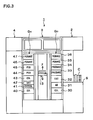
- FIG. 3 is a rear view of the coating and developing treatment system in FIG. 1;
- FIG. 4 is an explanatory view of a vertical cross section of the resist coating unit
- FIG. 5 is an explanatory view of a horizontal cross section of the resist coating unit in FIG. 4;
- FIG. 6 is a plan view of a flow dividing plate used in the resist coating unit.
- FIG. 7 is an explanatory view of a vertical cross section showing another structure example of the resist coating unit.
- FIG. 1 is a plan view of a coating and developing treatment system 1 including a coating unit according to the present invention
- FIG. 2 is a front view of the coating and developing treatment system 1
- FIG. 3 is a rear view of the coating and developing treatment system 1 .
- the coating and developing treatment system 1 has a structure in which a cassette station 2 for carrying, for example, 25 wafers W in a unit of cassette from/to the outside to/from the coating and developing treatment system 1 and for carrying the wafers W to/from a cassette C, a processing station 3 composed of various kinds of processing units which are disposed in multi-tiers, for performing predetermined processing for the wafers W one by one in coating and developing processes, and an interface section 4 for delivering the wafers W to/from a not-shown aligner which is disposed adjacent to the processing station 3 are integrally connected.
- a cassette station 2 for carrying, for example, 25 wafers W in a unit of cassette from/to the outside to/from the coating and developing treatment system 1 and for carrying the wafers W to/from a cassette C
- a processing station 3 composed of various kinds of processing units which are disposed in multi-tiers, for performing predetermined processing for the wafers W one by one in coating and developing processes
- an interface section 4 for delivering the
- a plurality of the cassettes C are mountable in predetermined positions on a cassette mounting table 5 , which serves as a mounting portion, in a line in an X direction (a vertical direction in FIG. 1 ). Furthermore, a wafer carrier 7 , which is movable in the alignment direction of the cassettes (the X direction) and in an alignment direction of the wafers W housed in the cassette C (a Z direction; a perpendicular direction), is provided to be movable along a carrier path 8 so that it is selectively accessible to each of the cassettes C.
- the wafer carrier 7 has an alignment function for aligning the wafers W.
- the wafer carrier 7 is structured so as to be also accessible to an extension unit 32 included in a third processing unit group G 3 on a processing station 3 side as will be described later.
- a main carrier 13 is provided in a center part thereof, and various kinds of the processing units are multi-tiered on a periphery of the main carrier 13 to constitute a processing unit group.
- the first and the second processing unit groups G 1 and G 2 are disposed on a front side of the coating and developing treatment system 1
- the third processing unit group G 3 is disposed adjacent to the cassette station 2
- the fourth processing unit group G 4 is disposed adjacent to the interface section 4 .
- a fifth processing unit group G 5 depicted by the broken line is allowed to be additionally disposed on a rear side as an option.
- the main carrier 13 is capable of carrying the wafers W to/from various kinds of later described processing units which are disposed in these processing unit groups G 1 , G 2 , G 3 , and G 4 .
- the number and the arrangement of the processing unit groups vary depending on which kind of processing is performed on the wafers W and the number of the processing unit groups is optionally selective accordingly.
- a resist coating unit 17 serving as a coating unit according to this embodiment and a developing unit 18 for developing the wafers W after exposure processing are two-tiered in the order from the bottom.
- a resist coating unit 19 and a developing unit 20 are two-tiered in the order from the bottom.
- a cooling unit 30 for cooling the wafers W, an adhesion unit 31 for increasing fixability between a resist solution and the wafers W, the extension unit 32 for keeping the wafers W on standby therein, pre-baking units 33 and 34 for drying a solvent in the resist solution, post-baking units. 35 and 36 for performing heat treatment after the developing treatment, and so on are, for example, seven-tiered in the order from the bottom.
- a cooling unit 40 for example, a cooling unit 40 , an extension and cooling unit 41 for spontaneously cooling the mounted wafers W, an extension unit 42 , a cooling unit 43 , post-exposure baking units 44 and 45 for performing heat treatment after the exposure processing, post-baking units 46 and 47 , and so on are, for example, eight-tiered in the order from the bottom.
- a wafer carrier 50 is provided in a center part of the interface section 4 .
- the wafer carrier 50 is structured so as to be movable in the X direction (the vertical direction in FIG. 1) and the Z direction (the perpendicular direction), and to be rotatable in a ⁇ direction (a rotational direction about an axis Z), so that it is accessible to the extension and cooling unit 41 and the extension unit 42 which are included in the fourth processing.
- FIG. 4 is an explanatory view of a vertical cross section showing a schematic structure of the resist coating unit 17
- FIG. 5 is an explanatory view of a horizontal cross section of the resist coating unit 17 .
- a spin chuck 60 is provided with an upper surface thereof formed to be flat and with a not-shown suction port formed in a center part thereof so that the wafer W which is carried into the resist coating unit 17 is horizontally held by suction onto the spin chuck 60 .
- a not-shown drive mechanism which causes the spin chuck 60 to be movable vertically and rotatable is disposed so that the wafer W can be rotated at a predetermined rotational speed when the resist solution is applied on the wafer W and the spin chuck 60 is vertically movable when the wafer W is mounted onto the spin chuck 60 .
- a circular cup 61 with an upper part thereof being open is provided to surround the outer circumference of the spin chuck 60 so that the resist solution diffused by a centrifugal force from the rotated wafer W which is held by suction onto the spin chuck 60 is received therein and prevented from contaminating peripheral units.
- a not-shown drainpipe for draining out the resist solution which is spilled and diffused from the wafers W is formed.
- a first exhaust pipe 62 for exhausting an atmosphere inside the cup 61 is provided to extend from a bottom portion of the cup 61 .
- the first exhaust pipe 62 is communicated with a suction unit 63 via a second exhaust pipe 83 as described later so that the atmosphere inside the cup 61 can be actively exhausted by the suction unit 63 .
- a first damper 64 serving as a first adjusting device is provided to adjust a flow rate of gas flowing through the first exhaust pipe 62 .
- a case 66 which serves as an accommodating portion, having a rectangular parallelepiped outer shape which is oblong in the Y direction (a vertical direction in FIG. 5) as shown in FIG. 5 is provided.
- a nozzle carrier 68 which serves as a carrier, for carrying a resist solution supply nozzle 67 , which serves as a coating solution supply nozzle, for discharging the resist solution onto the wafer W.
- the nozzle carrier 68 includes a nozzle holding member 69 for holding the resist solution supply nozzle 67 to be suspended therefrom and an arm portion 70 to which the nozzle holding member 69 is fixed, as shown in FIG. 4 .
- a not-shown drive mechanism is provided in the arm portion 70 and the drive mechanism enables the arm portion 70 to move along a rail 71 which extends in the Y direction as shown in FIG. 5 and to expand and contract in the Z direction. Therefore, the resist solution supply nozzle 67 held by the nozzle holding member 69 is movable in the Y and Z directions.
- the nozzle holding member 69 is fixed in such a position that the nozzle holding member 69 is positioned above the center of the wafer W when the arm portion 70 moves to a position above the center of the wafer W so that the resist solution is supplied to the center of the wafer W from the resist solution supply nozzle 67 which is held by the nozzle holding member 69 .
- first ventilation holes 66 a are formed and a second ventilation hole 66 b is formed in a lower part on a cup 61 side of the case 66 so that gas from the first ventilation holes 66 a passes through the case 66 and is discharged from the second ventilation hole 66 b to an area below the cup 61 .
- a nozzle box 72 for keeping the above-mentioned resist solution supply nozzle 67 on stand-by therein is provided.
- a plurality of recessed portions 73 having the same outer shape as that of the resist solution supply nozzle 67 are formed so that the resist solution supply nozzle 67 is allowed to be received and kept on stand-by in the recessed portion 73 .
- the nozzle box 72 is structured to be movable in the X direction and the X direction movement of the nozzle box 72 causes a desired resist solution supply nozzle 67 to be positioned below the nozzle holding member 69 which is fixed to the nozzle carrier 68 and enables the descending nozzle holding member 69 to hold the resist solution supply nozzle 67 .
- a supply pipe 74 which serves as a supply device, for supplying predetermined gas, for example, air, which is the atmosphere, and inert gas, into the casing 17 a , is provided to extend from an upper surface of the casing 17 a .
- a damper 75 is attached to adjust a flow rate of the gas supplied into the casing 17 a to a predetermined flow rate.
- the inert gas for example, nitrogen gas, helium gas, and the like are usable.
- a temperature/humidity adjusting device 76 is disposed so that the gas flowing through the supply pipe 74 can be supplied into the casing 17 a after being adjusted to appropriate temperature and humidity.
- a flow dividing plate 77 for dividing the gas supplied from the supply pipe 74 is provided to be parallel to the upper surface of the casing 17 a .
- a number of ventilation holes 78 are formed as shown in FIG. 6 and the ventilation holes 78 are more densely formed in an area facing the cup 61 , which is placed below the flow dividing plate, than in other areas.
- This structure causes the gas supplied from the supply pipe 74 to be divided by passing through each of the ventilation holes 78 so that a stable descending air current is formed in the entire casing 17 a . More of the ventilation holes 78 are disposed in the area facing the cup 61 to supply more gas into the cup 61 .
- a current plate 80 is disposed horizontally to surround the outer circumference of the cup 61 .
- a number of holes 81 are formed as shown in FIG. 5 and the gas after passing through the flow dividing plate 77 passes through the holes 81 so that a linear descending air current is formed from the flow dividing plate 77 to the current plate 80 .
- a second exhaust pipe 83 which serves as a second exhaust pipe, with an exhaust port 82 thereof facing upward is provided to extend from an inner bottom portion of the casing 17 a so that an atmosphere inside the casing 17 a can be actively exhausted by the suction unit 63 .
- a second damper 84 which serves as a second adjusting device, for adjusting a flow rate of the atmosphere flowing through the second exhaust pipe 83 is attached.
- a downstream side of the first exhaust pipe 62 which extends from the cup 61 is communicated with the second exhaust pipe 83 on an upstream side of the second damper 84 and the atmosphere inside the cup 61 is also exhausted through the second exhaust pipe 83 in the end.
- the gas from the first exhaust pipe 62 is confluent with the second exhaust pipe 83 but the exhaust flow rate of the first exhaust pipe 62 is adjusted by the first damper 64 which is provided on the upstream side so that the second damper 84 adjusts only the flow rate of the atmosphere inside the casing 17 a which is exhausted from the exhaust port 82 .
- the first damper 64 in the first exhaust pipe 62 , the damper 75 in the supply pipe 74 , and the second damper 84 in the second exhaust pipe 83 described above are controlled by a controller 85 and the controller 85 enables the flow rates of the air currents flowing through the first exhaust pipe 62 , the second exhaust pipe 83 , and the supply pipe 74 to be maintained at predetermined flow rates and the flow rates to be changed to predetermined flow rates at predetermined timing.
- the wafer carrier 7 takes out one unprocessed wafer W from the cassette C and carries it to the adhesion unit 31 which is included in the third processing unit group G 3 .
- the wafer W which is coated with an adhesion promoter such as HMDS for improving fixability with the resist solution in the adhesion unit 31 , is carried to the cooling unit 30 by the main carrier 13 and cooled to predetermined temperature. Thereafter, the wafer W is carried to the resist coating unit 17 or 19 .
- the wafer W with the resist film formed thereon is carried again to the pre-baking unit 33 or 34 and the extension and cooling unit 41 in sequence by the main carrier 13 to undergo predetermined processing.
- the wafer W is taken out from the extension and cooling unit 41 by the wafer carrier 50 and carried to the aligner (not-shown) via the peripheral aligner 51 .
- the wafer W after undergoing the exposure processing is carried to the extension unit 42 by the wafer carrier 50 and further carried to the post-exposure baking unit 44 or 45 , the developing unit 18 or 20 , the post-baking unit 35 , 36 , 46 , or 47 , and the cooling unit 30 in sequence by the main carrier 13 to undergo predetermined processing in each of the units.
- the wafer W is returned to the cassette C by the wafer carrier 7 via the extension unit 32 and a series of predetermined coating and developing treatment is finished.
- the supply of the air whose temperature and humidity is adjusted is started into the casing 17 a from the supply pipe 74 before the wafer W is carried to the resist coating unit 17 .
- the flow rate of the supplied air at this time is adjusted to, for example, 2.1 m 3 /min. by the controller 85 and the damper 75 so that the speed of the air flowing through the supply pipe 74 is, for example, made to be approximately 0.3 m/s.
- the suction unit 63 starts to operate so that the atmosphere inside the cup 61 is exhausted from the first exhaust pipe 62 and the atmosphere inside the casing 17 a starts to be exhausted from the exhaust port 82 .
- the flow rate inside the first exhaust pipe 62 is adjusted to, for example, 1.5 m 3 /min., which is a first flow rate
- the flow rate inside the second exhaust pipe 83 is adjusted to, for example, 2.0 m 3 /min, which is a second flow rate.
- the air of 2.1 m 3 /min. which is supplied from the supply pipe 74 passes through the flow dividing plate 77 to be supplied into the entire casing 17 a , and the air of 1.5 m 3 /min. out of the supplied air flows into the cup 61 and is exhausted from the first exhaust pipe 62 while purging the inside of the cup 61 .
- the air of 0.5 m 3 /min. (a difference between the first flow rate and the second flow rate) out of the supplied air passes through the current plate 80 or the case 66 and is exhausted from the exhaust port 82 through the second exhaust pipe 83 while forming the descending air current inside the casing 17 a .
- the remaining air of 0.1 m 3 /min. serves for maintaining the pressure inside the casing 17 a at the positive pressure.
- the resist coating treatment for the wafer W is started after the atmospheres inside the casing 17 a and the cup 61 are maintained in appropriate conditions.
- the wafer W is carried into the resist coating unit 17 by the main carrier 13 , delivered to the spin chuck 60 which is ascended and kept on stand-by in advance, and thereafter held by suction onto the spin chuck 60 .
- the spin chuck 60 is descended to place the wafer W in a predetermined position inside the cup 61 .
- the nozzle carrier 68 moves in the Y direction to hold the resist solution supply nozzle 67 which is kept on stand-by in the nozzle box 72 . Then, it moves in the Y direction again to transfer the resist solution supply nozzle 67 to a position above the center of the wafer W.
- the rotation of the wafer W is started at a predetermined rotational speed, for example, at 100 rpm, by the spin chuck 60 .
- the exhaust flow rate in the first exhaust pipe 62 is increased, for example, from 1.5 m 3 /min. to 2.0 m 3 /min. by the first damper 64 .
- the resist solution is discharged from the resist solution supply nozzle 67 and a predetermined amount of the resist solution is supplied onto the center of the wafer W.
- the rotational speed of the wafer W is increased to, for example, 4,000 rpm, after the predetermined amount of the resist solution is supplied so that the resist solution on the wafer W is diffused onto the entire surface of the wafer W to form the resist film.
- the rotational speed of the wafer W is reduced to, for example, 2,500 rpm and the resist solution is further diffused to make the resist film thin.
- the exhaust flow rate inside the first exhaust pipe 62 is decreased from 2.0 m 3 /min. to 1.5 m 3 /min.
- the resist solution supply nozzle 67 is transferred again to the nozzle box 73 to be returned to the recessed portion 74 of the nozzle box 73 .
- the wafer W on which the resist film is formed is ascended by the spin chuck 60 again and delivered to the main carrier 13 from the spin chuck 60 .
- the resist coating treatment is finished when the wafer W is carried from the resist coating unit 17 to the pre-baking unit 33 where the subsequent process is carried out.
- the second exhaust pipe 83 for exhausting the atmosphere inside the casing 17 a and the first exhaust pipe 62 for exhausting the atmosphere inside the cup 61 are separately provided so that the pressure inside the casing 17 a can be adjusted to the positive pressure with the use of only the second exhaust pipe 83 . Therefore, the first exhaust pipe 62 does not need to be burdened with both of the works of exhausting the atmosphere inside the cup 61 and performing the positive pressure adjustment, as is conventionally required, so that the atmospheres inside the casing 17 a and the cup 61 can easily be adjusted.
- the first exhaust pipe 62 is provided to be connected to the second exhaust pipe 83 so that the atmospheres inside the cup 61 and the casing 17 a can finally be exhausted from one exhaust pipe, and thereby only one piping system is required for exhausting the atmospheres.
- the current plate 80 is provided around the cup 61 so that the descending air current inside the casing 17 a which is formed by providing the second exhaust pipe 82 is uniformly formed inside the casing 17 a . This enables impurities inside the casing 17 a to be appropriately discharged.
- the exhaust flow rate inside the cup 61 is increased only when the resist solution is supplied onto the rotated wafer W and the resist solution is diffused so that mist, which is produced from the resist solution in a large amount at the above timing, is prevented from flowing out of the cup 61 into the casing 17 a.
- the first exhaust pipe 62 is provided to be connected to the second exhaust pipe 83 as described above but the first exhaust pipe 62 and the second exhaust pipe 83 may be provided independently without being connected to each other.
- the pressure inside the casing 17 a and the exhaust flow rate inside the cup 61 can also be adjusted by different exhaust pipes, which makes it possible to facilitate the atmosphere control while the resist treatment is carried out, compared with a conventional art.
- the atmosphere inside the case 66 of the nozzle carrier 68 is exhausted by the second exhaust pipe 83 similarly to the atmosphere inside the casing 17 a but an exhaust pipe for exhausting the atmosphere inside the case 66 may separately be provided.
- an exhaust pipe 90 serving as a third exhaust pipe is provided to extend from a lower part of a side surface of the case 66 so that the atmosphere inside the case 66 can actively be exhausted, for example, by the suction unit 63 .
- the atmosphere inside the case 66 needs to be constantly exhausted and purged. Thereby, a clean atmosphere can be maintained around the nozzle carrier 68 which includes many drive mechanisms and in which impurities are easily produced and the impurities are prevented from adhering to the wafer W inside the cup 61 .
- the atmosphere inside the case 66 may constantly be exhausted while the resist coating treatment is performed, as described above, but may be exhausted only when the resist solution supply nozzle 67 which is held by the nozzle carrier 68 is placed above the wafer W. In other words, the atmosphere inside the case 66 is exhausted only when the impurities produced in the nozzle carrier 68 tend to easily drop onto the wafer W. Thereby, the atmosphere is prevented from being exhausted unnecessarily and excessively to stabilize the air current inside the casing 17 a and reduce power consumption which is required for exhausting.
- the coating unit applies the resist solution on the wafer W to form the resist film
- the present invention is applicable to a coating unit for applying a coating solution other than the resist solution, for example, a developing solution. It is also applicable to a coating unit for substrates other than the wafer W, for example, an LCD substrate.
- different pipes are usable for exhausting the atmosphere inside the casing to maintain the pressure inside the casing at the positive pressure and exhausting the atmosphere inside the cup to prevent the atmosphere inside the cup from flowing out, which makes it possible to realize easier atmosphere control satisfying a plurality of conditions.
- the atmospheres inside the casing and the cup can be exhausted only with one piping system so that a piping facility thereof is simplified and unnecessary facilities can be omitted to realize cost reduction.
Priority Applications (1)
| Application Number | Priority Date | Filing Date | Title |
|---|---|---|---|
| US10/801,817 US6982102B2 (en) | 2000-10-10 | 2004-03-17 | Coating unit and coating method |
Applications Claiming Priority (2)
| Application Number | Priority Date | Filing Date | Title |
|---|---|---|---|
| JP2000-309091 | 2000-10-10 | ||
| JP2000309091A JP3587776B2 (ja) | 2000-10-10 | 2000-10-10 | 塗布装置及び塗布方法 |
Related Child Applications (1)
| Application Number | Title | Priority Date | Filing Date |
|---|---|---|---|
| US10/801,817 Division US6982102B2 (en) | 2000-10-10 | 2004-03-17 | Coating unit and coating method |
Publications (2)
| Publication Number | Publication Date |
|---|---|
| US20020041935A1 US20020041935A1 (en) | 2002-04-11 |
| US6752872B2 true US6752872B2 (en) | 2004-06-22 |
Family
ID=18789306
Family Applications (2)
| Application Number | Title | Priority Date | Filing Date |
|---|---|---|---|
| US09/972,866 Expired - Lifetime US6752872B2 (en) | 2000-10-10 | 2001-10-10 | Coating unit and coating method |
| US10/801,817 Expired - Fee Related US6982102B2 (en) | 2000-10-10 | 2004-03-17 | Coating unit and coating method |
Family Applications After (1)
| Application Number | Title | Priority Date | Filing Date |
|---|---|---|---|
| US10/801,817 Expired - Fee Related US6982102B2 (en) | 2000-10-10 | 2004-03-17 | Coating unit and coating method |
Country Status (3)
| Country | Link |
|---|---|
| US (2) | US6752872B2 (ja) |
| JP (1) | JP3587776B2 (ja) |
| KR (1) | KR100786455B1 (ja) |
Cited By (20)
| Publication number | Priority date | Publication date | Assignee | Title |
|---|---|---|---|---|
| US20060189103A1 (en) * | 2005-02-18 | 2006-08-24 | Tokyo Electron Limited | Solution treatment apparatus and solution treatment method |
| US20090000543A1 (en) * | 2007-06-29 | 2009-01-01 | Sokudo Co., Ltd. | Substrate treating apparatus |
| US20090028671A1 (en) * | 2006-12-15 | 2009-01-29 | Samsung Electronics Co., Ltd. | In-line system and method for manufacturing a semiconductor package |
| US20090139450A1 (en) * | 2007-11-30 | 2009-06-04 | Sokudo Co., Ltd. | Multi-story substrate treating apparatus with flexible transport mechanisms |
| US20090139833A1 (en) * | 2007-11-30 | 2009-06-04 | Sokudo Co., Ltd. | Multi-line substrate treating apparatus |
| US20090142933A1 (en) * | 2007-11-29 | 2009-06-04 | Masayoshi Yajima | Manufacturing apparatus for semiconductor device and manufacturing method for semiconductor device |
| US20090162547A1 (en) * | 2005-12-15 | 2009-06-25 | Ikuo Sawada | Coating Apparatus and Coating Method |
| US20090165712A1 (en) * | 2007-12-28 | 2009-07-02 | Sokudo Co., Ltd. | substrate treating apparatus with parallel substrate treatment lines |
| US20090165711A1 (en) * | 2007-12-28 | 2009-07-02 | Sokudo Co., Ltd. | Substrate treating apparatus with substrate reordering |
| US7651306B2 (en) | 2004-12-22 | 2010-01-26 | Applied Materials, Inc. | Cartesian robot cluster tool architecture |
| US7694647B2 (en) | 2004-12-22 | 2010-04-13 | Applied Materials, Inc. | Cluster tool architecture for processing a substrate |
| US7699021B2 (en) | 2004-12-22 | 2010-04-20 | Sokudo Co., Ltd. | Cluster tool substrate throughput optimization |
| US7798764B2 (en) | 2005-12-22 | 2010-09-21 | Applied Materials, Inc. | Substrate processing sequence in a cartesian robot cluster tool |
| US7819079B2 (en) | 2004-12-22 | 2010-10-26 | Applied Materials, Inc. | Cartesian cluster tool configuration for lithography type processes |
| US8597429B2 (en) | 2011-01-18 | 2013-12-03 | Nuflare Technology, Inc. | Manufacturing apparatus and method for semiconductor device |
| US20150090305A1 (en) * | 2013-09-27 | 2015-04-02 | Tokyo Electron Limited | Liquid processing apparatus |
| US20170028450A1 (en) * | 2015-07-29 | 2017-02-02 | Tokyo Electron Limited | Liquid processing apparatus |
| US11047050B2 (en) * | 2018-10-30 | 2021-06-29 | Taiwan Semiconductor Manufacturing Co., Ltd. | Semiconductor tool having controllable ambient environment processing zones |
| US20220187705A1 (en) * | 2018-06-21 | 2022-06-16 | Inpria Corporation | Stable solutions of monoalkyl tin alkoxides and their hydrolysis and condensation products |
| US20220216052A1 (en) * | 2013-03-14 | 2022-07-07 | Taiwan Semiconductor Manufacturing Co., Ltd. | Integrate Rinse Module in Hybrid Bonding Platform |
Families Citing this family (18)
| Publication number | Priority date | Publication date | Assignee | Title |
|---|---|---|---|---|
| JP2004072120A (ja) * | 2002-07-22 | 2004-03-04 | Yoshitake Ito | 現像方法及び現像装置及び液処理方法及び液処理装置 |
| US7077585B2 (en) * | 2002-07-22 | 2006-07-18 | Yoshitake Ito | Developing method and apparatus for performing development processing properly and a solution processing method enabling enhanced uniformity in the processing |
| JP2007036268A (ja) * | 2002-07-22 | 2007-02-08 | Yoshitake Ito | 基板処理方法及び基板処理装置 |
| US7041172B2 (en) * | 2003-02-20 | 2006-05-09 | Asml Holding N.V. | Methods and apparatus for dispensing semiconductor processing solutions with multi-syringe fluid delivery systems |
| KR100802151B1 (ko) | 2003-03-06 | 2008-02-11 | 니폰 쇼쿠바이 컴파니 리미티드 | 불소-함유 폴리이미드 필름의 제조 방법 및 장치 |
| TWI278416B (en) * | 2004-12-09 | 2007-04-11 | Au Optronics Corp | Cassette stocker |
| JP4979079B2 (ja) | 2007-07-09 | 2012-07-18 | 東京エレクトロン株式会社 | 基板処理装置 |
| JP4812704B2 (ja) * | 2007-07-10 | 2011-11-09 | 東京エレクトロン株式会社 | 基板処理装置 |
| JP5195010B2 (ja) * | 2008-05-13 | 2013-05-08 | 東京エレクトロン株式会社 | 塗布装置、塗布方法及び記憶媒体 |
| JP5369538B2 (ja) | 2008-08-12 | 2013-12-18 | 東京エレクトロン株式会社 | 液処理装置及び液処理方法並びに記憶媒体 |
| JP5641556B2 (ja) * | 2009-09-30 | 2014-12-17 | 株式会社Screenホールディングス | 基板処理装置 |
| CN108080222A (zh) * | 2016-11-23 | 2018-05-29 | 沈阳芯源微电子设备有限公司 | 一种废液收集杯的排风切换装置及其方法 |
| CN106707690B (zh) | 2017-01-04 | 2021-08-20 | 中国科学院光电技术研究所 | 光刻胶涂覆方法和装置 |
| JP7124946B2 (ja) * | 2017-08-10 | 2022-08-24 | 東京エレクトロン株式会社 | 液処理方法 |
| TWI693627B (zh) * | 2018-11-22 | 2020-05-11 | 辛耘企業股份有限公司 | 流體收集裝置 |
| JP7232737B2 (ja) * | 2019-08-07 | 2023-03-03 | 東京エレクトロン株式会社 | 基板処理装置 |
| JP7441665B2 (ja) * | 2020-02-10 | 2024-03-01 | 株式会社Screenホールディングス | 基板処理装置 |
| KR102576155B1 (ko) * | 2021-06-07 | 2023-09-07 | 세메스 주식회사 | 기판 처리 장치 |
Citations (6)
| Publication number | Priority date | Publication date | Assignee | Title |
|---|---|---|---|---|
| US5472502A (en) * | 1993-08-30 | 1995-12-05 | Semiconductor Systems, Inc. | Apparatus and method for spin coating wafers and the like |
| US5565034A (en) * | 1993-10-29 | 1996-10-15 | Tokyo Electron Limited | Apparatus for processing substrates having a film formed on a surface of the substrate |
| US5672205A (en) | 1994-09-29 | 1997-09-30 | Tokyo Electron Limited | Coating apparatus |
| US5690995A (en) * | 1995-01-13 | 1997-11-25 | Gema Volstatic Ag | Spray booth for powder coating |
| US6159541A (en) * | 1997-10-31 | 2000-12-12 | Tokyo Electron Limited | Spin coating process |
| US6333003B1 (en) * | 1997-05-22 | 2001-12-25 | Tokyo Electron Limited | Treatment apparatus, treatment method, and impurity removing apparatus |
Family Cites Families (7)
| Publication number | Priority date | Publication date | Assignee | Title |
|---|---|---|---|---|
| JP2764069B2 (ja) * | 1989-07-06 | 1998-06-11 | 東京エレクトロン株式会社 | 塗布方法 |
| KR0140519B1 (ko) * | 1989-09-25 | 1998-07-15 | 고다까 토시오 | 도포장치 |
| JPH04174848A (ja) | 1990-11-08 | 1992-06-23 | Fujitsu Ltd | レジスト塗布装置 |
| JPH05166712A (ja) | 1991-12-18 | 1993-07-02 | Dainippon Screen Mfg Co Ltd | 回転塗布方法 |
| JP2952626B2 (ja) * | 1992-10-20 | 1999-09-27 | 東京エレクトロン株式会社 | 処理装置 |
| JPH09148231A (ja) | 1995-11-16 | 1997-06-06 | Dainippon Screen Mfg Co Ltd | 回転式基板処理装置 |
| JPH09205062A (ja) | 1996-01-26 | 1997-08-05 | Tokyo Electron Ltd | レジスト塗布装置 |
-
2000
- 2000-10-10 JP JP2000309091A patent/JP3587776B2/ja not_active Expired - Fee Related
-
2001
- 2001-10-09 KR KR1020010062011A patent/KR100786455B1/ko active IP Right Grant
- 2001-10-10 US US09/972,866 patent/US6752872B2/en not_active Expired - Lifetime
-
2004
- 2004-03-17 US US10/801,817 patent/US6982102B2/en not_active Expired - Fee Related
Patent Citations (6)
| Publication number | Priority date | Publication date | Assignee | Title |
|---|---|---|---|---|
| US5472502A (en) * | 1993-08-30 | 1995-12-05 | Semiconductor Systems, Inc. | Apparatus and method for spin coating wafers and the like |
| US5565034A (en) * | 1993-10-29 | 1996-10-15 | Tokyo Electron Limited | Apparatus for processing substrates having a film formed on a surface of the substrate |
| US5672205A (en) | 1994-09-29 | 1997-09-30 | Tokyo Electron Limited | Coating apparatus |
| US5690995A (en) * | 1995-01-13 | 1997-11-25 | Gema Volstatic Ag | Spray booth for powder coating |
| US6333003B1 (en) * | 1997-05-22 | 2001-12-25 | Tokyo Electron Limited | Treatment apparatus, treatment method, and impurity removing apparatus |
| US6159541A (en) * | 1997-10-31 | 2000-12-12 | Tokyo Electron Limited | Spin coating process |
Cited By (44)
| Publication number | Priority date | Publication date | Assignee | Title |
|---|---|---|---|---|
| US7925377B2 (en) | 2004-12-22 | 2011-04-12 | Applied Materials, Inc. | Cluster tool architecture for processing a substrate |
| US8550031B2 (en) | 2004-12-22 | 2013-10-08 | Applied Materials, Inc. | Cluster tool architecture for processing a substrate |
| US7651306B2 (en) | 2004-12-22 | 2010-01-26 | Applied Materials, Inc. | Cartesian robot cluster tool architecture |
| US8911193B2 (en) | 2004-12-22 | 2014-12-16 | Applied Materials, Inc. | Substrate processing sequence in a cartesian robot cluster tool |
| US7819079B2 (en) | 2004-12-22 | 2010-10-26 | Applied Materials, Inc. | Cartesian cluster tool configuration for lithography type processes |
| US7743728B2 (en) | 2004-12-22 | 2010-06-29 | Applied Materials, Inc. | Cluster tool architecture for processing a substrate |
| US7694647B2 (en) | 2004-12-22 | 2010-04-13 | Applied Materials, Inc. | Cluster tool architecture for processing a substrate |
| US7699021B2 (en) | 2004-12-22 | 2010-04-20 | Sokudo Co., Ltd. | Cluster tool substrate throughput optimization |
| US7547614B2 (en) | 2005-02-18 | 2009-06-16 | Tokyo Electron Limited | Solution treatment apparatus and solution treatment method |
| US20090214759A1 (en) * | 2005-02-18 | 2009-08-27 | Tokyo Electron Limited | Solution treatment apparatus and solution treatment method |
| US7736498B2 (en) | 2005-02-18 | 2010-06-15 | Tokyo Electron Limited | Solution treatment apparatus and solution treatment method |
| US20060189103A1 (en) * | 2005-02-18 | 2006-08-24 | Tokyo Electron Limited | Solution treatment apparatus and solution treatment method |
| US20090162547A1 (en) * | 2005-12-15 | 2009-06-25 | Ikuo Sawada | Coating Apparatus and Coating Method |
| US7798764B2 (en) | 2005-12-22 | 2010-09-21 | Applied Materials, Inc. | Substrate processing sequence in a cartesian robot cluster tool |
| US8066466B2 (en) | 2005-12-22 | 2011-11-29 | Applied Materials, Inc. | Substrate processing sequence in a Cartesian robot cluster tool |
| US20090028671A1 (en) * | 2006-12-15 | 2009-01-29 | Samsung Electronics Co., Ltd. | In-line system and method for manufacturing a semiconductor package |
| US10290521B2 (en) | 2007-06-29 | 2019-05-14 | Screen Semiconductor Solutions Co., Ltd. | Substrate treating apparatus with parallel gas supply pipes and a gas exhaust pipe |
| US9174235B2 (en) | 2007-06-29 | 2015-11-03 | Screen Semiconductor Solutions Co., Ltd. | Substrate treating apparatus using horizontal treatment cell arrangements with parallel treatment lines |
| US20090000543A1 (en) * | 2007-06-29 | 2009-01-01 | Sokudo Co., Ltd. | Substrate treating apparatus |
| US9230834B2 (en) | 2007-06-29 | 2016-01-05 | Screen Semiconductor Solutions Co., Ltd. | Substrate treating apparatus |
| US9165807B2 (en) | 2007-06-29 | 2015-10-20 | Screen Semiconductor Solutions Co., Ltd. | Substrate treating apparatus with vertical treatment arrangement including vertical blowout and exhaust units |
| US8851008B2 (en) * | 2007-06-29 | 2014-10-07 | Sokudo Co., Ltd. | Parallel substrate treatment for a plurality of substrate treatment lines |
| US20090142933A1 (en) * | 2007-11-29 | 2009-06-04 | Masayoshi Yajima | Manufacturing apparatus for semiconductor device and manufacturing method for semiconductor device |
| US7967912B2 (en) * | 2007-11-29 | 2011-06-28 | Nuflare Technology, Inc. | Manufacturing apparatus for semiconductor device and manufacturing method for semiconductor device |
| US9687874B2 (en) | 2007-11-30 | 2017-06-27 | Screen Semiconductor Solutions Co., Ltd. | Multi-story substrate treating apparatus with flexible transport mechanisms and vertically divided treating units |
| US9184071B2 (en) | 2007-11-30 | 2015-11-10 | Screen Semiconductor Solutions Co., Ltd. | Multi-story substrate treating apparatus with flexible transport mechanisms and vertically divided treating units |
| US20090139450A1 (en) * | 2007-11-30 | 2009-06-04 | Sokudo Co., Ltd. | Multi-story substrate treating apparatus with flexible transport mechanisms |
| US20090139833A1 (en) * | 2007-11-30 | 2009-06-04 | Sokudo Co., Ltd. | Multi-line substrate treating apparatus |
| US20090165712A1 (en) * | 2007-12-28 | 2009-07-02 | Sokudo Co., Ltd. | substrate treating apparatus with parallel substrate treatment lines |
| US9299596B2 (en) | 2007-12-28 | 2016-03-29 | Screen Semiconductor Solutions Co., Ltd. | Substrate treating apparatus with parallel substrate treatment lines simultaneously treating a plurality of substrates |
| US9368383B2 (en) | 2007-12-28 | 2016-06-14 | Screen Semiconductor Solutions Co., Ltd. | Substrate treating apparatus with substrate reordering |
| US20090165711A1 (en) * | 2007-12-28 | 2009-07-02 | Sokudo Co., Ltd. | Substrate treating apparatus with substrate reordering |
| US8597429B2 (en) | 2011-01-18 | 2013-12-03 | Nuflare Technology, Inc. | Manufacturing apparatus and method for semiconductor device |
| US20220216052A1 (en) * | 2013-03-14 | 2022-07-07 | Taiwan Semiconductor Manufacturing Co., Ltd. | Integrate Rinse Module in Hybrid Bonding Platform |
| US11854795B2 (en) * | 2013-03-14 | 2023-12-26 | Taiwan Semiconductor Manufacturing Company, Ltd. | Integrate rinse module in hybrid bonding platform |
| US9773687B2 (en) * | 2013-09-27 | 2017-09-26 | Tokyo Electron Limited | Liquid processing apparatus |
| US20150090305A1 (en) * | 2013-09-27 | 2015-04-02 | Tokyo Electron Limited | Liquid processing apparatus |
| US10297473B2 (en) | 2013-09-27 | 2019-05-21 | Tokyo Electron Limited | Liquid processing apparatus |
| US10046372B2 (en) * | 2015-07-29 | 2018-08-14 | Tokyo Electron Limited | Liquid processing apparatus |
| US20170028450A1 (en) * | 2015-07-29 | 2017-02-02 | Tokyo Electron Limited | Liquid processing apparatus |
| US20220187705A1 (en) * | 2018-06-21 | 2022-06-16 | Inpria Corporation | Stable solutions of monoalkyl tin alkoxides and their hydrolysis and condensation products |
| US11868046B2 (en) * | 2018-06-21 | 2024-01-09 | Inpria Corporation | Stable solutions of monoalkyl tin alkoxides and their hydrolysis and condensation products |
| US11047050B2 (en) * | 2018-10-30 | 2021-06-29 | Taiwan Semiconductor Manufacturing Co., Ltd. | Semiconductor tool having controllable ambient environment processing zones |
| US11814731B2 (en) | 2018-10-30 | 2023-11-14 | Taiwan Semiconductor Manufacturing Company, Ltd. | Semiconductor tool having controllable ambient environment processing zones |
Also Published As
| Publication number | Publication date |
|---|---|
| US20040175497A1 (en) | 2004-09-09 |
| KR20020028807A (ko) | 2002-04-17 |
| JP2002118051A (ja) | 2002-04-19 |
| KR100786455B1 (ko) | 2007-12-17 |
| US20020041935A1 (en) | 2002-04-11 |
| JP3587776B2 (ja) | 2004-11-10 |
| US6982102B2 (en) | 2006-01-03 |
Similar Documents
| Publication | Publication Date | Title |
|---|---|---|
| US6752872B2 (en) | Coating unit and coating method | |
| US6682629B2 (en) | Substrate processing unit | |
| US20060127575A1 (en) | Substrate coating unit and substrate coating method | |
| US6541376B2 (en) | Film forming method and film forming apparatus | |
| US6632281B2 (en) | Substrate processing apparatus and substrate processing method | |
| KR100861046B1 (ko) | 기판의 처리 방법 및 기판의 처리 장치 | |
| US6527860B1 (en) | Substrate processing apparatus | |
| US20070137556A1 (en) | Thermal processing appparatus | |
| US6467976B2 (en) | Coating and developing system | |
| JP2010130014A (ja) | ノズル、及びそれを利用する基板処理装置及び処理液吐出方法 | |
| US6875281B2 (en) | Method and system for coating and developing | |
| US6485203B2 (en) | Substrate processing method and substrate processing apparatus | |
| JPH0536597A (ja) | 処理方法 | |
| JP2005011996A (ja) | 塗布処理方法及び塗布処理装置 | |
| JP3504863B2 (ja) | レジスト塗布方法及び基板処理装置 | |
| KR20180119788A (ko) | 공조 장치 및 그것을 갖는 기판 처리 장치 | |
| JP3718633B2 (ja) | 基板処理方法及び基板処理装置 | |
| KR100590711B1 (ko) | 처리시스템 | |
| KR20220154449A (ko) | 기판 처리 장치 | |
| JP2004165614A (ja) | 基板の処理装置及び基板の処理方法 | |
| JP2001210584A (ja) | シリル化処理装置及びシリル化処理方法 |
Legal Events
| Date | Code | Title | Description |
|---|---|---|---|
| AS | Assignment |
Owner name: TOKYO ELECTRON LIMITED, JAPAN Free format text: ASSIGNMENT OF ASSIGNORS INTEREST;ASSIGNORS:INADA, HIROICHI;HAYASHI, SHINICHI;REEL/FRAME:012622/0536 Effective date: 20010911 |
|
| STCF | Information on status: patent grant |
Free format text: PATENTED CASE |
|
| FEPP | Fee payment procedure |
Free format text: PAYER NUMBER DE-ASSIGNED (ORIGINAL EVENT CODE: RMPN); ENTITY STATUS OF PATENT OWNER: LARGE ENTITY Free format text: PAYOR NUMBER ASSIGNED (ORIGINAL EVENT CODE: ASPN); ENTITY STATUS OF PATENT OWNER: LARGE ENTITY |
|
| FPAY | Fee payment |
Year of fee payment: 4 |
|
| FPAY | Fee payment |
Year of fee payment: 8 |
|
| FPAY | Fee payment |
Year of fee payment: 12 |