US6515641B1 - Image display apparatus and method of driving image display apparatus - Google Patents
Image display apparatus and method of driving image display apparatus Download PDFInfo
- Publication number
- US6515641B1 US6515641B1 US09/511,246 US51124600A US6515641B1 US 6515641 B1 US6515641 B1 US 6515641B1 US 51124600 A US51124600 A US 51124600A US 6515641 B1 US6515641 B1 US 6515641B1
- Authority
- US
- United States
- Prior art keywords
- signal
- modulator
- potential
- display devices
- column wirings
- Prior art date
- Legal status (The legal status is an assumption and is not a legal conclusion. Google has not performed a legal analysis and makes no representation as to the accuracy of the status listed.)
- Expired - Lifetime
Links
- 238000000034 method Methods 0.000 title description 24
- 239000010409 thin film Substances 0.000 description 15
- 239000011159 matrix material Substances 0.000 description 14
- 239000000126 substance Substances 0.000 description 9
- 239000000758 substrate Substances 0.000 description 9
- 230000007423 decrease Effects 0.000 description 7
- 238000010586 diagram Methods 0.000 description 7
- 238000010894 electron beam technology Methods 0.000 description 7
- 239000002184 metal Substances 0.000 description 6
- 238000009826 distribution Methods 0.000 description 4
- 239000010408 film Substances 0.000 description 4
- XOLBLPGZBRYERU-UHFFFAOYSA-N tin dioxide Chemical compound O=[Sn]=O XOLBLPGZBRYERU-UHFFFAOYSA-N 0.000 description 4
- 230000000694 effects Effects 0.000 description 3
- 230000004044 response Effects 0.000 description 3
- 238000009429 electrical wiring Methods 0.000 description 2
- 239000000463 material Substances 0.000 description 2
- 230000000007 visual effect Effects 0.000 description 2
- OKTJSMMVPCPJKN-UHFFFAOYSA-N Carbon Chemical compound [C] OKTJSMMVPCPJKN-UHFFFAOYSA-N 0.000 description 1
- 229910052799 carbon Inorganic materials 0.000 description 1
- 239000004020 conductor Substances 0.000 description 1
- 230000003247 decreasing effect Effects 0.000 description 1
- 230000004927 fusion Effects 0.000 description 1
- 239000011521 glass Substances 0.000 description 1
- 238000010438 heat treatment Methods 0.000 description 1
- PJXISJQVUVHSOJ-UHFFFAOYSA-N indium(III) oxide Inorganic materials [O-2].[O-2].[O-2].[In+3].[In+3] PJXISJQVUVHSOJ-UHFFFAOYSA-N 0.000 description 1
- 239000012212 insulator Substances 0.000 description 1
- 239000004973 liquid crystal related substance Substances 0.000 description 1
- 238000004519 manufacturing process Methods 0.000 description 1
- 229910044991 metal oxide Inorganic materials 0.000 description 1
- 150000004706 metal oxides Chemical class 0.000 description 1
- 238000004377 microelectronic Methods 0.000 description 1
- 239000012299 nitrogen atmosphere Substances 0.000 description 1
- 230000000704 physical effect Effects 0.000 description 1
- 239000007787 solid Substances 0.000 description 1
- 238000004544 sputter deposition Methods 0.000 description 1
Images


Classifications
-
- G—PHYSICS
- G09—EDUCATION; CRYPTOGRAPHY; DISPLAY; ADVERTISING; SEALS
- G09G—ARRANGEMENTS OR CIRCUITS FOR CONTROL OF INDICATING DEVICES USING STATIC MEANS TO PRESENT VARIABLE INFORMATION
- G09G3/00—Control arrangements or circuits, of interest only in connection with visual indicators other than cathode-ray tubes
- G09G3/20—Control arrangements or circuits, of interest only in connection with visual indicators other than cathode-ray tubes for presentation of an assembly of a number of characters, e.g. a page, by composing the assembly by combination of individual elements arranged in a matrix no fixed position being assigned to or needed to be assigned to the individual characters or partial characters
- G09G3/22—Control arrangements or circuits, of interest only in connection with visual indicators other than cathode-ray tubes for presentation of an assembly of a number of characters, e.g. a page, by composing the assembly by combination of individual elements arranged in a matrix no fixed position being assigned to or needed to be assigned to the individual characters or partial characters using controlled light sources
-
- G—PHYSICS
- G09—EDUCATION; CRYPTOGRAPHY; DISPLAY; ADVERTISING; SEALS
- G09G—ARRANGEMENTS OR CIRCUITS FOR CONTROL OF INDICATING DEVICES USING STATIC MEANS TO PRESENT VARIABLE INFORMATION
- G09G2310/00—Command of the display device
- G09G2310/02—Addressing, scanning or driving the display screen or processing steps related thereto
- G09G2310/0264—Details of driving circuits
- G09G2310/027—Details of drivers for data electrodes, the drivers handling digital grey scale data, e.g. use of D/A converters
-
- G—PHYSICS
- G09—EDUCATION; CRYPTOGRAPHY; DISPLAY; ADVERTISING; SEALS
- G09G—ARRANGEMENTS OR CIRCUITS FOR CONTROL OF INDICATING DEVICES USING STATIC MEANS TO PRESENT VARIABLE INFORMATION
- G09G2320/00—Control of display operating conditions
- G09G2320/02—Improving the quality of display appearance
- G09G2320/0223—Compensation for problems related to R-C delay and attenuation in electrodes of matrix panels, e.g. in gate electrodes or on-substrate video signal electrodes
-
- G—PHYSICS
- G09—EDUCATION; CRYPTOGRAPHY; DISPLAY; ADVERTISING; SEALS
- G09G—ARRANGEMENTS OR CIRCUITS FOR CONTROL OF INDICATING DEVICES USING STATIC MEANS TO PRESENT VARIABLE INFORMATION
- G09G2320/00—Control of display operating conditions
- G09G2320/02—Improving the quality of display appearance
- G09G2320/0233—Improving the luminance or brightness uniformity across the screen
-
- G—PHYSICS
- G09—EDUCATION; CRYPTOGRAPHY; DISPLAY; ADVERTISING; SEALS
- G09G—ARRANGEMENTS OR CIRCUITS FOR CONTROL OF INDICATING DEVICES USING STATIC MEANS TO PRESENT VARIABLE INFORMATION
- G09G2320/00—Control of display operating conditions
- G09G2320/06—Adjustment of display parameters
- G09G2320/0626—Adjustment of display parameters for control of overall brightness
-
- G—PHYSICS
- G09—EDUCATION; CRYPTOGRAPHY; DISPLAY; ADVERTISING; SEALS
- G09G—ARRANGEMENTS OR CIRCUITS FOR CONTROL OF INDICATING DEVICES USING STATIC MEANS TO PRESENT VARIABLE INFORMATION
- G09G3/00—Control arrangements or circuits, of interest only in connection with visual indicators other than cathode-ray tubes
- G09G3/20—Control arrangements or circuits, of interest only in connection with visual indicators other than cathode-ray tubes for presentation of an assembly of a number of characters, e.g. a page, by composing the assembly by combination of individual elements arranged in a matrix no fixed position being assigned to or needed to be assigned to the individual characters or partial characters
- G09G3/2007—Display of intermediate tones
- G09G3/2011—Display of intermediate tones by amplitude modulation
-
- G—PHYSICS
- G09—EDUCATION; CRYPTOGRAPHY; DISPLAY; ADVERTISING; SEALS
- G09G—ARRANGEMENTS OR CIRCUITS FOR CONTROL OF INDICATING DEVICES USING STATIC MEANS TO PRESENT VARIABLE INFORMATION
- G09G3/00—Control arrangements or circuits, of interest only in connection with visual indicators other than cathode-ray tubes
- G09G3/20—Control arrangements or circuits, of interest only in connection with visual indicators other than cathode-ray tubes for presentation of an assembly of a number of characters, e.g. a page, by composing the assembly by combination of individual elements arranged in a matrix no fixed position being assigned to or needed to be assigned to the individual characters or partial characters
- G09G3/2007—Display of intermediate tones
- G09G3/2014—Display of intermediate tones by modulation of the duration of a single pulse during which the logic level remains constant
Definitions
- the present invention relates to an image display apparatus and a method of driving the image display apparatus, particularly, to an image display apparatus constituted by commonly wiring a plurality of display devices and a driving method thereof, more particularly, to an image display apparatus having a display panel constituted by wiring a plurality of display devices in a matrix and a driving method thereof and, still more particularly, to an image display apparatus capable of displaying a television signal and computer video signal with high quality and a driving method thereof.
- thermionic and cold cathode devices are known as electron-emitting devices.
- cold cathode devices are surface-conduction type emission devices, field emission type electron-emitting devices (to be referred to as FE type electron-emitting devices hereinafter), and metal/insulator/metal type electron-emitting devices (to be referred to as MIM type electron-emitting devices hereinafter).
- the surface-conduction type emission device utilizes the phenomenon that electrons are emitted by a small-area thin film formed on a substrate by flowing a current parallel through the film surface.
- the surface-conduction type emission device includes electron-emitting devices using an Au thin film (G. Dittmer, “Thin Solid Films”, 9,317 (1972)), an In 2 O 3 /SnO 2 thin film (M. Hartwell and C. G. Fonstad, “IEEE Trans. ED Conf.”, 519 (1975)), a carbon thin film (Hisashi Araki et al., “Vacuum”, Vol. 26, No. 1, p. 22 (1983)), and the like, in addition to an SnO 2 thin film according to Elinson mentioned above.
- FIG. 11 is a plan view showing the device by M. Hartwell et al. described above as a typical example of the device structures of these surface-conduction type emission devices.
- reference numeral 3001 denotes a substrate; and 3004 , a conductive thin film made of a metal oxide formed by sputtering.
- This conductive thin film 3004 has an H-shaped pattern, as shown in FIG. 11 .
- An electron-emitting portion 3005 is formed by performing electrification processing (referred to as forming processing to be described later) with respect to the conductive thin film 3004 .
- An interval L in FIG. 11 is set to 0.5 to 1 mm, and a width W is set to 0.1 mm.
- the electron-emitting portion 3005 is shown in a rectangular shape at the center of the conductive thin film 3004 for the sake of illustrative convenience. However, this does not exactly show the actual position and shape of the electron-emitting portion.
- the electron-emitting portion 3005 is formed by performing electrification processing called forming processing for the conductive thin film 3004 before electronemission.
- forming processing a constant DC voltage or a DC voltage which increases at a very low rate of, e.g., 1 V/min is applied across the conductive thin film 3004 to partially destroy or deform the conductive thin film 3004 , thereby forming the electron-emitting portion 3005 with an electrically high resistance.
- the destroyed or deformed part of the conductive thin film 3004 has a fissure.
- electrons are emitted near the fissure.
- FIG. 12 is a sectional view showing the device by C. A. Spindt et al. described above as a typical example of the FE type device structure.
- reference numeral 3010 denotes a substrate; 3011 , an emitter wiring made of a conductive material; 3012 , an emitter cone; 3013 , an insulating layer; and 3014 , a gate electrode.
- a voltage is applied between the emitter cone 3012 and gate electrode 3014 to emit electrons from the distal end portion of the emitter cone 3012 .
- an emitter and gate electrode are arranged on a substrate to be almost parallel to the surface of the substrate, in addition to the multilayered structure of FIG. 12 .
- FIG. 13 shows a typical example of the MIM type device structure.
- reference numeral 3020 denotes a substrate; 3021 , a lower electrode made of a metal; 3022 , a thin insulating layer having a thickness of about 100 ⁇ ; and 3023 , an upper electrode made of a metal and having a thickness of about 80 to 300 ⁇ .
- an appropriate voltage is applied between the upper and lower electrodes 3023 and 3021 to emit electrons from the surface of the upper electrode 3023 .
- the cold cathode device Since the above-described cold cathode devices can emit electrons at a temperature lower than that for thermionic cathode devices, they do not require any heater.
- the cold cathode device has a structure simpler than that of the thermionic cathode device and can shrink in feature size. Even if a large number of devices are arranged on a substrate at a high density, problems such as heat fusion of the substrate hardly arise.
- the response speed of the cold cathode device is high, while the response speed of the thermionic cathode device is low because the thermionic cathode device operates upon heating by a heater.
- the surface-conduction type emission devices have a simple structure and can be easily manufactured, and thus many devices can be formed on a wide area.
- Japanese Patent Laid-Open No. 64-31332 filed by the assignee of the present application a method of arranging and driving a lot of devices has been studied.
- an image display apparatus using a combination of a surface-conduction type emission device and a fluorescent substance which emits light upon irradiation of an electron beam has been studied.
- This type of image display apparatus using a combination of the surface-conduction type emission device and fluorescent substance is expected to exhibit more excellent characteristics than other conventional image display apparatuses.
- the above display apparatus is superior in that it does not require any backlight because it is of a self-emission type and that it has a wide view angle.
- a method of driving a plurality of FE type electron-emitting devices arranged side by side is disclosed in, e.g., U.S. Pat. No. 4,904,895 filed by the assignee of the present application.
- FE type electron-emitting devices to an image display apparatus is a flat panel display reported by R. Meyer et al. (R. Meyer: “Recent Development on Microtips Display at LETI”, Tech. Digest of 4th Int. Vacuum Microelectronics Conf., Nagahama, pp. 6-9 (1991)).
- One aspect of an image display apparatus according to the present invention comprises the following arrangement.
- An image display apparatus comprises a row wiring, a plurality of column wirings, a modulator, and a plurality of display devices, the plurality of display devices being commonly connected to the row wiring, each of the plurality of column wirings being connected to a corresponding one of the plurality of display devices, and the modulator supplying a modulated signal to the column wirings,
- the modulator includes a pulse width modulator for generating a pulse signal having a time width corresponding to a tone of a signal to be displayed, and a potential setting circuit for setting a potential of the pulse signal in accordance with a type of signal to be displayed.
- the pulse width modulator and potential setting circuit, or the modulator including them may be one integrated circuit.
- the modulator and another circuit may be integrated into one.
- the potential of a pulse signal having a modulated time width may be adjusted by the potential setting circuit.
- a pulse width signal having a modulated time width may be generated at a potential set in advance by the potential setting circuit. This aspect incorporates both the arrangements. Note that the potential to be applied to the column wiring is set while a predetermined signal is supplied to the row wiring and the plurality of display devices can be driven. In particular, when a high-level period is to be changed in pulse width modulation, a high-level potential is set.
- the “high level” of the signal means a level corresponding to a signal which drives the device or a signal for a high driving state, with respect to a low level corresponding to a signal which does not drive the device or a signal for a low driving state.
- Low- and high-level signals do not always have lower and higher potentials, respectively.
- the tone is controlled by the pulse width of a pulse signal, and control corresponding to the type of signal to be displayed is executed by controlling the potential of a pulse signal.
- the influence on tone control caused by control corresponding to the type of signal to be displayed can be preferably suppressed.
- a longitudinal direction of the column wiring preferably crosses a longitudinal direction of the row wiring.
- the row wiring include a plurality of row wirings, a plurality of display devices be connected to each row wiring, and each of the plurality of display devices connected to the row wiring share a corresponding column wiring with each of a plurality of display devices connected to another row wiring.
- the matrix wiring has a plurality of row wirings, a plurality of column wirings extending to cross the row wirings, and display devices arranged in correspondence with the intersections of the row and column wirings.
- Each display device may be arranged at or near the intersection.
- the display device is connected at a corresponding intersection to row and column wirings crossing each other.
- the image display apparatus preferably further comprises a scanning circuit for supplying a scan signal for sequentially scanning the plurality of row wirings.
- this aspect can preferably employ a circuit for applying a selection potential to a selected row wiring.
- This aspect can preferably adopt an arrangement in which the display device is driven by a voltage applied to it owing to the difference between the selection potential and the potential of a pulse signal supplied to the column wiring.
- a predetermined non-selection potential is preferably applied to an unselected row wiring.
- the above aspect can be preferably applied when the display device consumes only part of a current flowing into the display device for display.
- a current (particularly, a current not consumed by the display device for display) flows through the row wiring to increase the influence of the voltage drop on the row wiring which applies the potential to one end of each of a plurality of simultaneously drivable devices.
- This arrangement can preferably adopt the aspect of the present invention in which the pulse width can be adjusted in accordance with the type of signal.
- the present invention is effective in an arrangement in which a row wiring commonly connected to a plurality of simultaneously drivable display devices flows even a small current which is not consumed by the display device for display.
- the present invention is especially effective when 20% or more of a current flows into the display device, and more preferably 50% or more of the current flows through the column or row wiring without consuming the current for display.
- the present invention can be preferably applied.
- the current consumed by the display device for display includes a current consumed as heat in display operation.
- Each aspect can preferably employ an arrangement in which the apparatus further comprises a plurality of input portions for inputting an image signal to be displayed, and a selector for selecting any one of signals from the plurality of input portions, and the potential setting circuit sets the potential of the pulse signal in accordance with a selection state of the selector, an arrangement in which the apparatus further comprises a discrimination circuit for discriminating a characteristic of an image signal to be displayed, and the potential of the pulse signal is set in accordance with a discrimination result of the discrimination circuit, or an arrangement in which the apparatus further comprises external setting means for setting the potential of the pulse signal in accordance with an image to be displayed, and the potential setting circuit sets the potential of the pulse signal in accordance with a setting of the external setting means.
- the potential setting circuit desirably sets the potential in accordance with whether importance is attached to luminance or reproducibility in displaying an input image signal.
- the potential set by the potential setting circuit is desirably set to have a larger potential difference from a potential applied to the row wiring than when reproducibility is more important than luminance.
- the potential setting circuit preferably sets the potential of the pulse signal in accordance with whether the signal to be displayed is a computer image signal or a television image signal. More specifically, when the computer image signal is to be displayed, the potential of a pulse signal is set to have a smaller potential difference from a potential applied to the row wiring than when the television image signal is to be displayed.
- Another aspect of an image display apparatus according to the present invention comprises the following arrangement.
- An image display apparatus comprises a row wiring, a plurality of column wirings, a modulator, and a plurality of display devices, the plurality of display devices being commonly connected to the row wiring, each of the plurality of column wirings being connected to a corresponding one of the plurality of display devices, and the modulator supplying a modulated signal to the column wirings,
- the modulator includes a potential setting circuit for setting a potential of a signal supplied to the row wiring in accordance with a type of signal to be displayed.
- This arrangement can preferably realize control corresponding to the type of image signal displayed by a signal supplied to the row wiring, independently of modulation control using a signal supplied to the column wiring.
- the modulator can adopt an arrangement of generating a pulse width-modulated signal having a time width corresponding to the tone of a signal to be displayed, and an arrangement of generating a peak value-modulated signal having a peak value corresponding to the tone of a signal to be displayed.
- the pulse width modulating arrangement is more desirable in terms of tone display.
- a longitudinal direction of the column wiring preferably crosses a longitudinal direction of the row wiring.
- This aspect can preferably be applied to an arrangement in which the row wiring includes a plurality of row wirings, a plurality of display devices are connected to each row wiring, and each of the plurality of display devices connected to the row wiring shares a corresponding column wiring with each of a plurality of display devices connected to another row wiring.
- the image display apparatus desirably further comprises a scanning circuit for supplying a scan signal for sequentially scanning the plurality of row wirings. More specifically, the scanning circuit can preferably adopt an arrangement of applying a selection potential to a selected row wiring. In this arrangement, the selection potential is set in accordance with the type of image signal to be displayed.
- Still another aspect of an image display apparatus according to the present invention comprises the following arrangement.
- An image display apparatus comprises a row wiring, a plurality of column wirings, a modulator, and a plurality of display devices, the plurality of display devices being commonly connected to the row wiring, each of the plurality of column wirings being connected to a corresponding one of the plurality of display devices, and the modulator supplying a modulated signal to the column wirings,
- the modulator includes a peak value modulator for generating a signal having a peak value corresponding to a tone of a signal to be displayed, and a peak value setting circuit for setting an upper limit of the peak value in accordance with a type of signal to be displayed.
- the upper limit of the peak value is relative.
- the upper value of the peak value is the upper limit of the potential.
- the upper limit of the peak value is the lower limit of the potential.
- the minimum value of the amplitude of the peak value may also be set.
- the above aspects of the present invention are preferable when the display device consumes 80% or less of a current flowing into the display device for display, and more preferable when the display device consumes 50% or less of a current flowing into the display device for display.
- the display device is, e.g., an electron-emitting device.
- This electron-emitting device is desirably used in combination with an emission substance (especially, a fluorescent substance) for emitting light upon irradiation of electrons emitted by the electron-emitting device.
- an emission substance especially, a fluorescent substance
- a cold cathode device can be preferably employed.
- the present invention is more preferable in an arrangement using a surface-conduction type emission device.
- the display device is an electron-emitting device, an image can be displayed with high quality using a fluorescent substance for emitting light upon irradiation of electrons emitted by the electron-emitting device.
- the display device is an electroluminescent device
- the above aspects can be preferably used.
- the display device is an electroluminescent device, since the device itself emits light, it is preferable.
- One aspect of a method of driving an image display apparatus according to the present invention is as follows.
- a method of driving an image display apparatus having a row wiring, a plurality of column wirings, a modulator, and a plurality of display devices, the plurality of display devices being commonly connected to the row wiring, each of the plurality of column wirings being connected to a corresponding one of the plurality of display devices, and the modulator supplying a modulated signal to the column wirings, comprises the step of
- Another aspect of a method of driving an image display apparatus according to the present invention is as follows.
- a method of driving an image display apparatus having a row wiring, a plurality of column wirings, a modulator, and a plurality of display devices, the plurality of display devices being commonly connected to the row wiring, each of the plurality of column wirings being connected to a corresponding one of the plurality of display devices, and the modulator supplying a modulated signal to the column wirings, comprises the step of
- Still another aspect of a method of driving an image display apparatus according to the present invention is as follows.
- a method of driving an image display apparatus having a row wiring, a plurality of column wirings, a modulator, and a plurality of display devices, the plurality of display devices being commonly connected to the row wiring, each of the plurality of column wirings being connected to a corresponding one of the plurality of display devices, and the modulator supplying a modulated signal to the column wirings, comprises the steps of
- the above-mentioned aspects are more preferable when the modulator outputs a potential-controlled signal (e.g., high-level potential) as a control target than when the modulator outputs a current-controlled signal as a control target.
- a potential-controlled signal e.g., high-level potential
- FIG. 1 is a block diagram for explaining an image display apparatus according to the first embodiment of the present invention
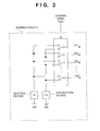
- FIG. 2 is a circuit diagram for explaining scanning circuits 2 and 2 ′ in the image display apparatus of the present invention
- FIG. 3 is a graph showing the typical characteristic of a surface-conduction type emission device used in the embodiment of the present invention.
- FIG. 4 is a partially cutaway perspective view showing the display panel of the image display apparatus according to the embodiment of the present invention.
- FIG. 5 is a circuit diagram for explaining an arrangement of an amplitude setting circuit (means) 9 according to the first embodiment of the present invention
- FIG. 6 is a graph showing the luminance distribution when a whole white pattern (R: 100%, G: 100%, B: 100%) is displayed by a display circuit according to the first embodiment of the present invention
- FIG. 7 is a graph showing the luminance decrease ratio when the whole white pattern (R: 100%, G: 100%, B: 100%) is displayed by the display circuit according to the first embodiment of the present invention.
- FIG. 8 is a block diagram for explaining an image display apparatus according to the second embodiment of the present invention.
- FIG. 9 is a diagram for explaining the electrical wiring of the display panel according to the present invention.
- FIG. 10 is a view for explaining the problem of the present invention.
- FIG. 11 is a plan view showing a conventionally known surface-conduction type emission device.
- FIG. 12 is a side view showing a conventionally known FE type device.
- FIG. 13 is a sectional view showing a conventionally known MIM type device.
- the present inventors have examined electron-emitting devices of various materials, various manufacturing methods, and various structures, in addition to the above-mentioned conventional electron-emitting device. Further, the present inventors have made extensive studies on a multi electron source having a large number of electron-emitting devices, and an image display apparatus using this multi electron source.
- the present inventors have examined a multi electron source having an electrical wiring method shown in, e.g., FIG. 9 . That is, a large number of electron-emitting devices are two-dimensionally arranged in a matrix to obtain a multi electron source, as shown in FIG. 9 .
- numeral 4001 denotes an electron-emitting device
- numeral 4002 denotes row wirings
- numeral 4003 denotes column wirings.
- Each of the row and column wirings 4002 and 4003 actually has finite electrical resistances, which are represented as wiring resistances 4004 and 4005 , respectively, in FIG. 9 .
- This wiring method is called a simple matrix wiring method.
- the multi electron source is illustrated in a 6 ⁇ 6 matrix, but the size of the matrix is not limited to this.
- a number of devices enough to perform a desired image display are arranged and wired.
- a selection potential Vs is applied to the row wiring 4002 on the row to be selected, and at the same time, a non-selection potential Vns is applied to the row wirings 4002 on unselected rows.
- a driving potential Ve for outputting an electron beam is applied to the column wirings 4003 .
- a multi electron source obtained by arranging electron-emitting devices in a simple matrix has a variety of applications. For example, when a potential signal corresponding to image information is appropriately applied, the multi electron source can be applied as an electron source for an image display apparatus.
- the electron-emitting devices As the first cause of varying the voltage applied to respective devices, the electron-emitting devices have different wiring lengths (different wiring resistances) in the simple matrix wiring.
- the magnitudes of voltage drops caused by the wiring resistances 4004 at the respective portions of the row wiring are nonuniform. This is because a current branches and flows from the row wiring of a selected row to respective electron-emitting devices connected to the row, and thus currents flowing through the respective wiring resistances 4004 become nonuniform.
- the magnitude of a voltage drop caused by the wiring resistance changes depending on a driving pattern (displayed image in the image display apparatus). This is because a current flowing through the wiring resistance changes depending on the driving pattern.
- the influence of a luminance decrease caused by the voltage drop is less conspicuous to a subjectively negligible degree on a natural image such as a general television broadcast, but often provides an unnatural image particularly in displaying a flat image represented by a computer output.
- FIG. 10 is a view for explaining this problem of the present invention.
- FIG. 10 shows an original image of a window screen that is a typical computer output image as an image to be displayed.
- the screen in FIG. 10 displays a window with a background of only blue (for RGB tonality, R: 0%, G: 0%, B: 100%) and a center of only white (for RGB tonality, R: 100%, G: 100%, B: 100%).
- a row including both the background and window and a row including only the background are compared to find that the blue luminance is different between them because of different voltage drop amounts caused by a display pattern difference regardless of the same blue color of the original image.
- the difference in luminance disadvantageously appears like steps at the boundary between horizontal lines of the window.
- a luminance decrease caused by the influence of the wiring resistance becomes more noticeable nearer the center of the screen, and the image changes with gradation as a whole.
- the human visual characteristic is very insensitive to this continuous change, and the image looks natural.
- a computer output image is displayed with a lower luminance than that of a general TV image owing to the application purpose.
- the following embodiments will exemplify an image display apparatus which can reduce an unnatural pattern generated upon displaying a computer image while considering the characteristics of the computer image, and can generally display an image having a wide dynamic range in displaying a natural image represented by an HDTV signal or another TV signal.
- the first embodiment concerns an example of modulation using a voltage pulse width-modulated signal as a modulated signal in order to obtain a desired image in a display apparatus having many surface-conduction type emission devices.
- FIG. 4 is a partially cutaway perspective view of the display panel used in the first embodiment showing the internal structure of the panel.
- reference numeral 1005 denotes a rear plate; 1006 , a side wall; and 1007 , a face plate.
- These parts 1005 to 1007 constitute an airtight container for maintaining the inside of the display panel vacuum.
- frit glass is applied to junction portions, and sintered at 400 to 500° C. in air or nitrogen atmosphere, thus the parts are seal-connected. A method for exhausting air from the inside of the container will be described later.
- the rear plate 1005 has a substrate 1001 fixed thereon, on which N ⁇ M cold cathode devices 1002 are formed.
- the N ⁇ M cold cathode devices are arranged in a simple matrix with M row wirings 1003 and N column wirings 1004 .
- the portion constituted by the components denoted by references 1001 to 1004 will be referred to as a multi electron source.
- a fluorescent film 1008 is formed on the lower surface of the face plate 1007 .
- the fluorescent film 1008 is coated with red, green, and blue fluorescent substances, i.e., three primary color fluorescent substances used in the CRT field.
- surface-conduction type emission devices are formed as cold cathode devices in the display panel having the above outer appearance.
- the surface-conduction type emission device has an (emission current Ie) vs. (device application voltage Vf) characteristic and (device current If) vs. (device application voltage Vf) characteristic as shown in FIG. 3 .
- the emission current Ie is very small, therefore it is difficult to illustrate the emission current Ie by the same measure of that for the device current If. For this reason, the graph illustrates two curves in different measures.
- the device has three characteristics:
- threshold voltage Vth a voltage of a predetermined level (referred to as “threshold voltage Vth”) or more is applied to the device.
- the emission current Ie drastically increases, however, with a voltage lower than the threshold voltage Vth, almost no emission current Ie is detected.
- Vth is 8 V.
- the device has a nonlinear characteristic based on the clear threshold voltage Vth.
- the emission current Ie changes in dependence upon the device application voltage Vf. Accordingly, the emission current Ie can be controlled by changing the voltage Vf.
- the emission current Ie quickly flows by application of the voltage Vf to the device. Accordingly, an amount of electrons to be emitted by the device can be controlled by changing period of application of the voltage Vf.
- the surface-conduction type emission device with these characteristics can be preferably applied to the display apparatus.
- the first characteristic is utilized, display by sequential scanning of the display screen is possible.
- the threshold voltage Vth or greater is appropriately applied to a driven device in accordance with a desired emission luminance, while a voltage lower than the threshold voltage Vth is applied to an unselected device.
- Devices to be driven are sequentially changed to sequentially scan the display screen, thereby performing display.
- the emission luminance can be controlled utilizing the second or third characteristic, which enables tone display.
- the first embodiment displays an image using the first and third characteristics of the surface-conduction type emission device.
- FIG. 1 is a block diagram schematically showing a circuit arrangement.
- reference numeral 1 denotes a display panel incorporating a multi electron source.
- Reference symbols Dx 1 to DxM′ denote row wiring terminals of the multi electron source;
- Dy 1 to DyN column wiring terminals of the multi electron source;
- Hv a high-voltage terminal for applying an accelerating voltage between face and rear plates;
- Va a high-voltage power source.
- Reference numerals 2 and 2 ′ denote scanning circuits; 3 , a sync signal separator; 4 , atiminggenerator; 7 , a converter for converting a YRB signal from the sync separator into an RGB signal; 13 , a signal switching unit for switching between an HDTV RGB signal (signal based on the High Definition Television System standard) and a VGA signal (signal based on the VGA (Video Graphic Array) standard); 5 , a shift register for one line of image data; 6 , a line memory for one line of image data; 8 , a pulse width modulator; 9 , an amplitude setting circuit; 10 , a controller; 11 , a remote controller interface; and 12 , a switch for controlling the image display apparatus.
- the first embodiment uses a surface-conduction type emission device as the electron-emitting device of the multi electron source.
- the image display apparatus of the first embodiment can display both an HDTV television signal and a VGA signal which is an output from a computer or the like. Note that this embodiment is merely an example, and the image display apparatus can be similarly applied to another standard such as NTSC, PAL, and SECAM.
- a VGA signal is supplied to the signal switching unit 13 , whereas sync signals Vsync and Hsync are supplied to the timing generator 4 .
- An HDTV television signal is separated into a sync signal Tsync (including vertical and horizontal sync signals) and video signal YRB by the sync separator 3 .
- the signal Tsync is supplied to the timing generator 4 .
- the video signal YRB is converted by the RGB converter 7 into a digital RGB signal, which is supplied to the signal switching unit 13 .
- the signal switching unit 13 selects between VGA and HDTV, and switches a video source in accordance with a selection signal Tsel from the controller 10 .
- the controller 10 supplies the selection signal Tsel to each unit after a video source to be selected is set through the remote controller 11 or switch 12 .
- the timing generator 4 determines the operation timing of each unit in synchronism with a video source sync signal on the selected side based on the selection signal Tsel. That is, the timing generator 4 generates signals such as a signal Tsft for controlling the operation timing of the shift register 5 , a signal Tmry for controlling the operation timing of the line memory 6 , and a signal Tscan for controlling the operation of the scanning circuit 2 .
- the scanning circuits 2 and 2 ′ output a selection potential Vs or non-selection potential Vns to the connected terminals Dx 1 to DxM′ in order to sequentially scan the multi electron source in units of rows.
- Each scanning circuit incorporates, e.g., M′ switches, as shown in FIG. 2 .
- Each switch is preferably made up of a transistor and FET.
- the values of the selection potential Vs and non-selection potential Vns output from the scanning circuits 2 and 2 ′, and the value of a modulated signal (to be described later) are determined based on the (emission current Ie) vs. (device application voltage Vf) characteristic and (device current If) vs. (device application voltage Vf) of a cold cathode device in use.
- the surface-conduction type emission device of the first embodiment requires a voltage of about +12 to +15 V as the device application voltage Vf in order to display a desired image.
- the selection potential and non-selection potential are respectively set to ⁇ 7.5 V and 0 V.
- a potential of +5 V to +7.5 V is applied during a time corresponding to image data to be displayed from the modulation side. Then, electrons are emitted to obtain a desired image.
- Image data separated by the sync signal separator 3 is serial/parallel-converted by the shift register 5 , and stored in the line memory 6 during one horizontal scanning period.
- the pulse width modulator 8 outputs pulse width-modulated voltage signals PW 1 to PWN on the basis of image data I′D 1 to I′DN stored in the line memory 6 .
- the potential VX is set in accordance with the selection signal Tsel.
- the potential VX is connected to a power source VX 1 through a switch SW-A; and when the video signal is a computer output such as a VGA signal, the potential VX is connected to a power source VX 2 .
- the potentials of VX 1 and VX 2 are respectively set to +7.5 V and +6 V.
- a computer output image is generally displayed at a low luminance as a whole because the user directly watches the monitor.
- an accelerating potential Va for accelerating electrons emitted by the electron-emitting device is decreased, image data (corresponding to a pulse width after pulse width modulation in the first embodiment) is reduced, or the application voltage is reduced.
- the present inventors have examined these methods to find that it is optimal to reduce the driving voltage (driving voltage for driving the device) applied to the display panel.
- an image In displaying a natural image represented by an HDTV signal or another television signal, driving is done at a higher driving voltage than in the computer display mode. Accordingly, an image can be preferably displayed with reality at high luminance.
- the display panel of the first embodiment has a so-called simple matrix structure in which cold cathode devices are arranged at the intersections of M row wirings and N column wirings. Displaying a high-quality image requires desired numbers of row and column wirings.
- the first embodiment has examined an image display apparatus having 480 row wirings and 2,556 (852 ⁇ 3) column wirings.
- the image display apparatus of this embodiment may suffer a voltage drop mainly caused by the wiring resistance of the row wiring, and thus the wiring resistance of the row wiring is preferably set as low as possible.
- the display panel examined in this embodiment has
- the surface-conduction type emission device as the cold cathode device in the first embodiment was manufactured with characteristics as shown in Table 1:
- HDTV and VGA signals were selected as video sources to display for each signal a whole white pattern (R: 100%, G: 100%, B: 100%, i.e., modulated signals on all the columns have a maximum pulse width). Then, the luminance of the display panel was measured to obtain the results in FIG. 6 .
- the abscissa represents the column number
- the ordinate represents the luminance. The luminance of the display panel is extracted and plotted along the abscissa. The ordinate adopts an arbitrary unit because the luminance changes depending on even the characteristics of the fluorescent substance and the characteristics of the metal back.
- driving is done at a lower driving voltage in the VGA display mode than in the HD display mode. This suppresses the whole luminance.
- the luminance decrease ratio on the entire screen upon displaying the whole white pattern is shown in FIG. 7 .
- the luminance decreases about 6.5% at the center of the screen in comparison with the two ends of the screen.
- the in-plane luminance distribution is suppressed to about 1.2% at the center and two ends of the screen.
- the in-plane luminance distribution takes at least a smaller value than 1.2% upon displaying another pattern. Even if the above-mentioned window is displayed, the in-plane luminance distribution can be reduced to 1.2% or less even on an unnatural pattern generated at the boundary of the horizontal line of the window.
- the present inventors actually displayed an image on this image display apparatus.
- an HDTV signal was displayed, an image having a wide dynamic range could be displayed with reality.
- a VGA signal was displayed, an unnatural pattern caused by the voltage drop on the wiring was hardly confirmed, and the image display apparatus could attain satisfactory characteristics as the output monitor of the computer.
- the voltage on the modulation means side is set in accordance with a video source selection state.
- the present invention is not limited to this, and can obtain the same effects even when the selection voltage source Vs on the scanning wiring side is used as a variable voltage source, and the value of the source Vs is changeable in accordance with a video source selection state.
- the amplitude is set by the two power sources VX 1 and VX 2 in FIG. 1 .
- the present invention is not limited to this, and the amplitude can be similarly set even by changing an output from one variable voltage source.
- the first embodiment has exemplified a computer output such as a VGA signal, and a television signal such as an HDTV or NTSC signal, and changes the driving conditions of the former and latter.
- a computer output such as a VGA signal
- a television signal such as an HDTV or NTSC signal
- driving conditions are changed in accordance with a selected video format, but may be changed in accordance with video contents.
- the driving voltage is set high in displaying an image with reality such as a sport program, and is set low in displaying a movie.
- This change allows the user to easily change the mode by issuing an instruction to the controller using the remote controller shown in FIG. 1 .
- a circuit for discriminating the type of image signal to be displayed may be adopted to switch the controller in accordance with the discrimination result.
- the discrimination circuit the present invention can use a circuit of extracting the characteristics of an input signal (e.g., the number of scanning lines, the number of sync signals, and sync signal timings) and discriminating the type of image signal based on the characteristics.
- the second embodiment concerns an example of modulation using a voltage amplitude-modulated signal as a modulated signal in order to obtain a desired image in a display apparatus having many surface-conduction type emission devices.
- FIG. 8 is a block diagram schematically showing a circuit arrangement.
- the second embodiment employs an amplitude modulator 21 instead of the pulse width modulator 8 in the first embodiment.
- Image data separated by a sync signal separator 3 is serial/parallel-converted by a shift register 5 , and stored in a line memory 6 during one horizontal scanning period.
- the amplitude modulator 21 D/A-converts the image data stored in the line memory 6 to output amplitude-modulated potential signals AM 1 to AMN.
- Two outputs Vr 1 and Vr 2 of an amplitude setting circuit 22 are connected to the reference terminal of a D/A converter.
- the amplitudes (potential values) of the amplitude-modulated potential signals AM 1 to AMN are modulated between minimum and maximum amplitudes Vr 2 and Vr 1 in accordance with image data, and supplied to respective column wirings.
- the output potential Vr 1 and Vr 2 of the amplitude modulator 21 are set to two different potentials in accordance with a selected video source.
- a computer output image is generally displayed at a low luminance as a whole because the user directly watches the monitor.
- the accelerating potential Va, driving voltage application time, or application voltage is reduced.
- the present inventors have examined these methods to find that it is optimal to reduce the driving voltage (driving voltage for driving the device) applied to the display panel.
- HD and VGA signals were selected as video sources by the driving circuit to display for each signal a whole white pattern (R: 100%, G: 100%, B 100%, i.e., modulated signals on all the columns have a maximum pulse width). Then, the luminance of the display panel was measured to obtain the results in FIG. 6 .
- the abscissa represents the column number
- the ordinate represents the luminance. The luminance of the display panel is extracted and plotted along the abscissa. The ordinate adopts an arbitrary unit because the luminance changes depending on even the characteristics of the fluorescent substance and the characteristics of the metal back.
- driving is done at a lower driving voltage in the VGA display mode than in the HD display mode. This suppresses the whole luminance.
- the luminance decrease ratio on the entire screen upon displaying the whole white pattern is shown in FIG. 7 .
- the luminance decreases about 6.5% at the center of the screen in comparison with the two ends of the screen.
- the in-plane luminance error is suppressed to about 1.2% at the center and two ends of the screen. Since even the driving method of this embodiment maximizes the voltage drop caused by the wiring resistance upon displaying the whole white pattern, the in-plane luminance error takes at least a smaller value than 1.2% upon displaying another pattern. Even if the above-mentioned window is displayed, the in-plane luminance error can be reduced to 1.2% or less even on an unnatural pattern generated at the boundary of the horizontal line of the window.
- the present inventors actually displayed an image on this image display apparatus.
- an HDTV signal was displayed, an image having a wide dynamic range could be displayed with reality.
- a VGA signal was displayed, an unnatural pattern caused by the voltage drop on the wiring was hardly confirmed, and the image display apparatus could attain satisfactory characteristics as the output monitor of the computer.
- the amplitude setting circuit (means) 22 of the second embodiment adjusts the amplitude in amplitude modulation by adjusting the reference potential of the amplitude modulator (means) 21 .
- the present invention is not limited to this.
- the amplitude modulator (means) 21 modulates the amplitude using a D/A converter having a fixed reference voltage
- the amplitude setting circuit 22 adjusts the amplitude using an amplifier capable of setting two gains and two offsets. Also in this case, the same effects could be obtained.
- the second embodiment has exemplified a computer output such as a VGA signal, and a television signal such as HDTV and NTSC signals, and changes the driving conditions of the former and latter.
- a computer output such as a VGA signal
- a television signal such as HDTV and NTSC signals
- changes the driving conditions of the former and latter changes the driving conditions of the former and latter.
- the present invention is not particularly limited to this, and different driving voltages may be set in accordance with various video formats.
- driving conditions are changed in accordance with a selected video format, but may be changed in accordance with video contents.
- the driving voltage is set high in displaying an image with reality such as a sport program, and is set low in displaying a movie.
- This change enables the user to easily change the mode by issuing an instruction to the controller using a remote controller shown in FIG. 7, and controlling respective units by the controller.
- the above-described image display apparatus displays a natural image represented by the above-mentioned HDTV signal or another TV signal
- the user can enjoy a wide-dynamic-range image with reality.
- the apparatus displays a computer image represented by a VGA signal
- the user hardly perceives any unnatural pattern caused by the voltage drop on the wiring.
- the apparatus can attain satisfactory characteristics as the output monitor of the computer.
- the present inventors have examined an application to an image display apparatus having a display panel in which electroluminescent devices (EL) were arranged in a simple matrix structure as the image display device of the display panel. As a result, the same effects as described above could be obtained.
- EL electroluminescent devices
Landscapes
- Engineering & Computer Science (AREA)
- Physics & Mathematics (AREA)
- Computer Hardware Design (AREA)
- General Physics & Mathematics (AREA)
- Theoretical Computer Science (AREA)
- Control Of Indicators Other Than Cathode Ray Tubes (AREA)
- Transforming Electric Information Into Light Information (AREA)
- Control Of El Displays (AREA)
Priority Applications (2)
| Application Number | Priority Date | Filing Date | Title |
|---|---|---|---|
| US10/241,536 US6933935B2 (en) | 1999-02-25 | 2002-09-12 | Image display apparatus and method of driving image display apparatus |
| US10/920,215 US7205987B2 (en) | 1999-02-25 | 2004-08-18 | Image display apparatus and method of driving image display apparatus |
Applications Claiming Priority (4)
| Application Number | Priority Date | Filing Date | Title |
|---|---|---|---|
| JP11-049067 | 1999-02-25 | ||
| JP4906799 | 1999-02-25 | ||
| JP2000-036861 | 2000-02-15 | ||
| JP2000036861A JP2000310969A (ja) | 1999-02-25 | 2000-02-15 | 画像表示装置及び画像表示装置の駆動方法 |
Related Child Applications (1)
| Application Number | Title | Priority Date | Filing Date |
|---|---|---|---|
| US10/241,536 Division US6933935B2 (en) | 1999-02-25 | 2002-09-12 | Image display apparatus and method of driving image display apparatus |
Publications (1)
| Publication Number | Publication Date |
|---|---|
| US6515641B1 true US6515641B1 (en) | 2003-02-04 |
Family
ID=26389417
Family Applications (3)
| Application Number | Title | Priority Date | Filing Date |
|---|---|---|---|
| US09/511,246 Expired - Lifetime US6515641B1 (en) | 1999-02-25 | 2000-02-23 | Image display apparatus and method of driving image display apparatus |
| US10/241,536 Expired - Fee Related US6933935B2 (en) | 1999-02-25 | 2002-09-12 | Image display apparatus and method of driving image display apparatus |
| US10/920,215 Expired - Fee Related US7205987B2 (en) | 1999-02-25 | 2004-08-18 | Image display apparatus and method of driving image display apparatus |
Family Applications After (2)
| Application Number | Title | Priority Date | Filing Date |
|---|---|---|---|
| US10/241,536 Expired - Fee Related US6933935B2 (en) | 1999-02-25 | 2002-09-12 | Image display apparatus and method of driving image display apparatus |
| US10/920,215 Expired - Fee Related US7205987B2 (en) | 1999-02-25 | 2004-08-18 | Image display apparatus and method of driving image display apparatus |
Country Status (2)
| Country | Link |
|---|---|
| US (3) | US6515641B1 (https=) |
| JP (1) | JP2000310969A (https=) |
Cited By (9)
| Publication number | Priority date | Publication date | Assignee | Title |
|---|---|---|---|---|
| US20030058211A1 (en) * | 2001-09-03 | 2003-03-27 | Sang-Il Kim | Liquid crystal display for wide viewing angle, and driving method thereof |
| US20040125046A1 (en) * | 2002-10-09 | 2004-07-01 | Canon Kabushiki Kaisha | Image display apparatus |
| US20040160406A1 (en) * | 2003-01-17 | 2004-08-19 | Canon Kabushiki Kaisha | Image display apparatus |
| US20040165004A1 (en) * | 2002-12-27 | 2004-08-26 | Canon Kabushiki Kaisha | Image display apparatus |
| US20050062700A1 (en) * | 1992-02-26 | 2005-03-24 | Naruhiko Kasai | Multiple-tone display system |
| US20050206634A1 (en) * | 2004-03-17 | 2005-09-22 | Canon Kabushiki Kaisha | Image display apparatus |
| US20060038836A1 (en) * | 2001-11-21 | 2006-02-23 | Canon Kabushiki Kaisha | Display apparatus, and image signal processing apparatus and drive control apparatus for the same |
| US20070238295A1 (en) * | 2006-04-11 | 2007-10-11 | Micron Technology, Inc. | Methods of forming semiconductor constructions |
| US20080150969A1 (en) * | 2006-12-13 | 2008-06-26 | Canon Kabushiki Kaisha | Image display apparatus and driving method of image display apparatus |
Families Citing this family (14)
| Publication number | Priority date | Publication date | Assignee | Title |
|---|---|---|---|---|
| US6985141B2 (en) * | 2001-07-10 | 2006-01-10 | Canon Kabushiki Kaisha | Display driving method and display apparatus utilizing the same |
| KR100490624B1 (ko) * | 2003-02-10 | 2005-05-17 | 삼성에스디아이 주식회사 | 화상 표시 장치 |
| JP4499480B2 (ja) * | 2003-11-27 | 2010-07-07 | オプトレックス株式会社 | 有機elディスプレイ装置の駆動装置 |
| KR100965591B1 (ko) * | 2003-12-22 | 2010-06-23 | 엘지디스플레이 주식회사 | 액정표시소자의 구동방법 및 장치 |
| KR20060001372A (ko) * | 2004-06-30 | 2006-01-06 | 삼성에스디아이 주식회사 | 배경휘도 저감형 전자 방출 장치 |
| US20080007616A1 (en) * | 2004-12-06 | 2008-01-10 | Ftd Technology Pte. Ltd. | Universal multimedia display adapter |
| WO2006098328A1 (ja) * | 2005-03-15 | 2006-09-21 | Sharp Kabushiki Kaisha | 表示装置の駆動装置、表示装置 |
| US20090122207A1 (en) * | 2005-03-18 | 2009-05-14 | Akihiko Inoue | Image Display Apparatus, Image Display Monitor, and Television Receiver |
| WO2006100906A1 (ja) * | 2005-03-18 | 2006-09-28 | Sharp Kabushiki Kaisha | 画像表示装置、画像表示モニター、およびテレビジョン受像機 |
| KR20060104840A (ko) * | 2005-03-31 | 2006-10-09 | 삼성에스디아이 주식회사 | 전자 방출 표시장치 및 그 제어 방법 |
| JP4722942B2 (ja) * | 2005-11-25 | 2011-07-13 | シャープ株式会社 | 画像表示方法、画像表示装置、画像表示モニター、および、テレビジョン受像機 |
| US20080192803A1 (en) * | 2006-10-24 | 2008-08-14 | Nabeel Agha Riza | Extreme Temperature Optical Sensor Designs And Signal Processing |
| JP5340083B2 (ja) * | 2009-08-28 | 2013-11-13 | キヤノン株式会社 | 画像表示装置及びその輝度制御方法 |
| US20160322163A1 (en) * | 2015-04-28 | 2016-11-03 | E I Du Pont De Nemours And Company | Terminal electrode of electronic component |
Citations (16)
| Publication number | Priority date | Publication date | Assignee | Title |
|---|---|---|---|---|
| JPS6431332A (en) | 1987-07-28 | 1989-02-01 | Canon Kk | Electron beam generating apparatus and its driving method |
| US4904895A (en) | 1987-05-06 | 1990-02-27 | Canon Kabushiki Kaisha | Electron emission device |
| JPH02257551A (ja) | 1989-03-30 | 1990-10-18 | Canon Inc | 画像形成装置 |
| JPH0355738A (ja) | 1989-03-30 | 1991-03-11 | Canon Inc | 電子源及びそれを用いた画像表示装置 |
| US5066883A (en) | 1987-07-15 | 1991-11-19 | Canon Kabushiki Kaisha | Electron-emitting device with electron-emitting region insulated from electrodes |
| JPH0428137A (ja) | 1990-05-23 | 1992-01-30 | Canon Inc | マルチ電子ビーム源及びこれを用いた画像表示装置 |
| US5311169A (en) * | 1988-06-07 | 1994-05-10 | Sharp Kabushiki Kaisha | Method and apparatus for driving capacitive display device |
| US5682085A (en) | 1990-05-23 | 1997-10-28 | Canon Kabushiki Kaisha | Multi-electron beam source and image display device using the same |
| US6100939A (en) * | 1995-09-20 | 2000-08-08 | Hitachi, Ltd. | Tone display method and apparatus for displaying image signal |
| US6169528B1 (en) * | 1995-08-23 | 2001-01-02 | Canon Kabushiki Kaisha | Electron generating device, image display apparatus, driving circuit therefor, and driving method |
| US6236385B1 (en) * | 1993-02-25 | 2001-05-22 | Seiko Epson Corporation | Method of driving a liquid crystal display device |
| US6246385B1 (en) * | 1997-04-28 | 2001-06-12 | Matsushita Electric Industrial Co., Ltd. | Liquid crystal display device and its driving method |
| US6262701B1 (en) * | 1994-12-05 | 2001-07-17 | Canon Kabushiki Kaisha | Electron-emission device and apparatus and image-formation using same |
| US6271812B1 (en) * | 1997-09-25 | 2001-08-07 | Denso Corporation | Electroluminescent display device |
| US6278474B1 (en) * | 1997-09-26 | 2001-08-21 | Minolta Co., Ltd. | Image forming apparatus provided with a plurality of light signal emitting heads |
| US6310598B1 (en) * | 1995-10-14 | 2001-10-30 | Semiconductor Energy Laboratory Co., Ltd. | Matrix type liquid-crystal display unit |
Family Cites Families (58)
| Publication number | Priority date | Publication date | Assignee | Title |
|---|---|---|---|---|
| US3590156A (en) * | 1968-08-28 | 1971-06-29 | Zenith Radio Corp | Flat panel display system with time-modulated gray scale |
| CA949159A (en) * | 1970-06-20 | 1974-06-11 | Teruo Sato | Scanning apparatus for dc el crossed-grid panel |
| US4006383A (en) * | 1975-11-28 | 1977-02-01 | Westinghouse Electric Corporation | Electroluminescent display panel with enlarged active display areas |
| US4206460A (en) * | 1977-03-10 | 1980-06-03 | Sharp Kabushiki Kaisha | EL Display drive controlled by an electron beam |
| US4114070A (en) * | 1977-03-22 | 1978-09-12 | Westinghouse Electric Corp. | Display panel with simplified thin film interconnect system |
| JPS5875194A (ja) * | 1981-10-30 | 1983-05-06 | 株式会社日立製作所 | マトリクス表示装置及び駆動方法 |
| US4528480A (en) * | 1981-12-28 | 1985-07-09 | Nippon Telegraph & Telephone | AC Drive type electroluminescent display device |
| US4554539A (en) * | 1982-11-08 | 1985-11-19 | Rockwell International Corporation | Driver circuit for an electroluminescent matrix-addressed display |
| US4652872A (en) * | 1983-07-07 | 1987-03-24 | Nec Kansai, Ltd. | Matrix display panel driving system |
| DE3511237A1 (de) * | 1984-03-29 | 1985-10-03 | Olympus Optical Co., Ltd., Tokio/Tokyo | Bildmarkierungsgeraet |
| US4646079A (en) * | 1984-09-12 | 1987-02-24 | Cornell Research Foundation, Inc. | Self-scanning electroluminescent display |
| JPS6180226A (ja) * | 1984-09-28 | 1986-04-23 | Toshiba Corp | アクテイブ・マトリツクス駆動装置 |
| FR2571913B1 (fr) * | 1984-10-17 | 1986-12-26 | Richard Joseph | Ecran d'affichage a matrice active a double transistor d'adressage |
| US4797667A (en) * | 1985-04-30 | 1989-01-10 | Planar Systems, Inc. | Split screen electrode structure for TFEL panel |
| JPH0634152B2 (ja) * | 1985-12-17 | 1994-05-02 | シャープ株式会社 | 薄膜el表示装置の駆動回路 |
| JPS6337394A (ja) * | 1986-08-01 | 1988-02-18 | 株式会社日立製作所 | マトリクス表示装置 |
| FR2608817B1 (fr) * | 1986-12-22 | 1989-04-21 | Thioulouse Pascal | Afficheur electroluminescent a memoire a tensions d'entretien multiples dephasees |
| US4975691A (en) * | 1987-06-16 | 1990-12-04 | Interstate Electronics Corporation | Scan inversion symmetric drive |
| JPH0518585Y2 (https=) | 1987-08-13 | 1993-05-18 | ||
| US5117298A (en) * | 1988-09-20 | 1992-05-26 | Nec Corporation | Active matrix liquid crystal display with reduced flickers |
| US4958105A (en) * | 1988-12-09 | 1990-09-18 | United Technologies Corporation | Row driver for EL panels and the like with inductance coupling |
| JPH0758635B2 (ja) * | 1989-11-24 | 1995-06-21 | 富士ゼロックス株式会社 | El駆動回路 |
| JPH0766246B2 (ja) * | 1989-12-15 | 1995-07-19 | 富士ゼロックス株式会社 | El駆動回路 |
| US5063378A (en) * | 1989-12-22 | 1991-11-05 | David Sarnoff Research Center, Inc. | Scanned liquid crystal display with select scanner redundancy |
| KR960004150B1 (ko) * | 1991-02-16 | 1996-03-27 | 가부시끼가이샤 한도다이 에네르기 겐꾸쇼 | 표시장치 |
| US5172032A (en) * | 1992-03-16 | 1992-12-15 | Alessio David S | Method of and apparatus for the energization of electroluminescent lamps |
| US5302966A (en) * | 1992-06-02 | 1994-04-12 | David Sarnoff Research Center, Inc. | Active matrix electroluminescent display and method of operation |
| JP3231088B2 (ja) | 1992-07-31 | 2001-11-19 | 株式会社リコー | 画像記録装置 |
| US6157137A (en) * | 1993-01-28 | 2000-12-05 | Canon Kabushiki Kaisha | Multi-electron beam source with driving circuit for preventing voltage spikes |
| KR0140041B1 (ko) * | 1993-02-09 | 1998-06-15 | 쯔지 하루오 | 표시 장치용 전압 발생 회로, 공통 전극 구동 회로, 신호선 구동 회로 및 계조 전압 발생 회로 |
| US5463279A (en) * | 1994-08-19 | 1995-10-31 | Planar Systems, Inc. | Active matrix electroluminescent cell design |
| JP2678574B2 (ja) | 1994-10-04 | 1997-11-17 | 近畿日本鉄道株式会社 | 調光装置 |
| US5703436A (en) * | 1994-12-13 | 1997-12-30 | The Trustees Of Princeton University | Transparent contacts for organic devices |
| US5684365A (en) * | 1994-12-14 | 1997-11-04 | Eastman Kodak Company | TFT-el display panel using organic electroluminescent media |
| DE69623153T2 (de) * | 1995-03-06 | 2003-04-17 | Thomson Multimedia, Boulogne | Treiberschaltungen für Datenleitungen mit einem gemeinsamen Rampensignal für ein Anzeigesystem |
| JPH08278772A (ja) | 1995-04-04 | 1996-10-22 | Mitsubishi Electric Corp | テレビ機能付きパソコン用モニター |
| US5959599A (en) * | 1995-11-07 | 1999-09-28 | Semiconductor Energy Laboratory Co., Ltd. | Active matrix type liquid-crystal display unit and method of driving the same |
| JP3342278B2 (ja) | 1996-01-11 | 2002-11-05 | キヤノン株式会社 | 画像表示装置及び該装置における画像表示方法 |
| JPH09190783A (ja) * | 1996-01-11 | 1997-07-22 | Canon Inc | 画像形成装置 |
| JPH09269755A (ja) | 1996-03-29 | 1997-10-14 | Seiko Epson Corp | 液晶表示装置 |
| US5723950A (en) * | 1996-06-10 | 1998-03-03 | Motorola | Pre-charge driver for light emitting devices and method |
| JPH09330063A (ja) | 1996-06-13 | 1997-12-22 | Fujitsu Ltd | 表示装置の駆動方法及びその回路 |
| JPH104528A (ja) | 1996-06-18 | 1998-01-06 | Matsushita Electric Ind Co Ltd | テレビジョン受像機 |
| JPH10117300A (ja) | 1996-10-08 | 1998-05-06 | Seiko Epson Corp | 画像表示装置 |
| JPH10319373A (ja) | 1997-03-18 | 1998-12-04 | Advanced Display:Kk | 液晶表示装置及び液晶表示システム |
| US5903246A (en) * | 1997-04-04 | 1999-05-11 | Sarnoff Corporation | Circuit and method for driving an organic light emitting diode (O-LED) display |
| US5952789A (en) * | 1997-04-14 | 1999-09-14 | Sarnoff Corporation | Active matrix organic light emitting diode (amoled) display pixel structure and data load/illuminate circuit therefor |
| JP3125711B2 (ja) | 1997-04-22 | 2001-01-22 | 日亜化学工業株式会社 | Ledディスプレイユニットとled定電流ドライバー回路 |
| US6229506B1 (en) * | 1997-04-23 | 2001-05-08 | Sarnoff Corporation | Active matrix light emitting diode pixel structure and concomitant method |
| JP3767877B2 (ja) * | 1997-09-29 | 2006-04-19 | 三菱化学株式会社 | アクティブマトリックス発光ダイオード画素構造およびその方法 |
| JPH11242207A (ja) * | 1997-12-26 | 1999-09-07 | Sony Corp | 電圧発生回路、光学空間変調素子、画像表示装置並びに画素の駆動方法 |
| JP3619085B2 (ja) * | 1999-02-18 | 2005-02-09 | キヤノン株式会社 | 画像形成装置、その製造方法及び記憶媒体 |
| JP4092857B2 (ja) * | 1999-06-17 | 2008-05-28 | ソニー株式会社 | 画像表示装置 |
| JP2001147659A (ja) * | 1999-11-18 | 2001-05-29 | Sony Corp | 表示装置 |
| US7015882B2 (en) * | 2000-11-07 | 2006-03-21 | Sony Corporation | Active matrix display and active matrix organic electroluminescence display |
| JP3593982B2 (ja) * | 2001-01-15 | 2004-11-24 | ソニー株式会社 | アクティブマトリクス型表示装置およびアクティブマトリクス型有機エレクトロルミネッセンス表示装置、並びにそれらの駆動方法 |
| JP3570394B2 (ja) * | 2001-05-25 | 2004-09-29 | ソニー株式会社 | アクティブマトリクス型表示装置およびアクティブマトリクス型有機エレクトロルミネッセンス表示装置、並びにそれらの駆動方法 |
| JP3610923B2 (ja) * | 2001-05-30 | 2005-01-19 | ソニー株式会社 | アクティブマトリクス型表示装置およびアクティブマトリクス型有機エレクトロルミネッセンス表示装置、並びにそれらの駆動方法 |
-
2000
- 2000-02-15 JP JP2000036861A patent/JP2000310969A/ja active Pending
- 2000-02-23 US US09/511,246 patent/US6515641B1/en not_active Expired - Lifetime
-
2002
- 2002-09-12 US US10/241,536 patent/US6933935B2/en not_active Expired - Fee Related
-
2004
- 2004-08-18 US US10/920,215 patent/US7205987B2/en not_active Expired - Fee Related
Patent Citations (17)
| Publication number | Priority date | Publication date | Assignee | Title |
|---|---|---|---|---|
| US4904895A (en) | 1987-05-06 | 1990-02-27 | Canon Kabushiki Kaisha | Electron emission device |
| US5066883A (en) | 1987-07-15 | 1991-11-19 | Canon Kabushiki Kaisha | Electron-emitting device with electron-emitting region insulated from electrodes |
| JPS6431332A (en) | 1987-07-28 | 1989-02-01 | Canon Kk | Electron beam generating apparatus and its driving method |
| US5311169A (en) * | 1988-06-07 | 1994-05-10 | Sharp Kabushiki Kaisha | Method and apparatus for driving capacitive display device |
| US5569974A (en) | 1989-03-30 | 1996-10-29 | Canon Kabushiki Kaisha | Electron-emitting device and electron beam lithograph machine and image display apparatus making use of it |
| JPH02257551A (ja) | 1989-03-30 | 1990-10-18 | Canon Inc | 画像形成装置 |
| JPH0355738A (ja) | 1989-03-30 | 1991-03-11 | Canon Inc | 電子源及びそれを用いた画像表示装置 |
| US5682085A (en) | 1990-05-23 | 1997-10-28 | Canon Kabushiki Kaisha | Multi-electron beam source and image display device using the same |
| JPH0428137A (ja) | 1990-05-23 | 1992-01-30 | Canon Inc | マルチ電子ビーム源及びこれを用いた画像表示装置 |
| US6236385B1 (en) * | 1993-02-25 | 2001-05-22 | Seiko Epson Corporation | Method of driving a liquid crystal display device |
| US6262701B1 (en) * | 1994-12-05 | 2001-07-17 | Canon Kabushiki Kaisha | Electron-emission device and apparatus and image-formation using same |
| US6169528B1 (en) * | 1995-08-23 | 2001-01-02 | Canon Kabushiki Kaisha | Electron generating device, image display apparatus, driving circuit therefor, and driving method |
| US6100939A (en) * | 1995-09-20 | 2000-08-08 | Hitachi, Ltd. | Tone display method and apparatus for displaying image signal |
| US6310598B1 (en) * | 1995-10-14 | 2001-10-30 | Semiconductor Energy Laboratory Co., Ltd. | Matrix type liquid-crystal display unit |
| US6246385B1 (en) * | 1997-04-28 | 2001-06-12 | Matsushita Electric Industrial Co., Ltd. | Liquid crystal display device and its driving method |
| US6271812B1 (en) * | 1997-09-25 | 2001-08-07 | Denso Corporation | Electroluminescent display device |
| US6278474B1 (en) * | 1997-09-26 | 2001-08-21 | Minolta Co., Ltd. | Image forming apparatus provided with a plurality of light signal emitting heads |
Non-Patent Citations (8)
| Title |
|---|
| C. A. Mead, "Operation of Tunnel-Emission Devices", Journal of Applied Physics, vol. 32, No. 4, pp. 646-652, 1961. |
| C. A. Spindt, et al., "Physical Properties of Thin-Film Field Emission Cathodes with Molybdenum Cones", Journal of Applied Physics, vol. 47, No. 12, pp. 5248-5263, 1976. |
| G. Dittmer, "Electrical Conduction and Electron Emission of Discontinuous Thin Films", Thin Solid Films, vol. 9, pp. 317-328, 1972. |
| H. Araki, "Electroforming and Electron Emission of Carbon Thin Films", Journal of the Vacuum Society of Japan, vol. 26, No. 1, pp. 22-29, 1981. |
| M. Hartwell, et al., "Strong Electon Emission From Patterned Tin-Indium Oxide Thin Films", International Electorn Devices Meeting, pp. 519-521, 1975. |
| M. I. Elinson, et al., "The Emission of Hot Electrons and the Field Emission of Electrons from Tin Oxide", Radio Engineering and Electronic Physics, pp. 1290-1296, 1965. |
| R. Myer, "Recent Development on "Microtips" Display at Leti", Technical Digest of IVMC 91, pp. 6-9, 1991. |
| W. P. Dyke, et al., "Field Emission", Advances in Electronics and Electron Physics, vol. VIII, pp. 89-185, 1956. |
Cited By (22)
| Publication number | Priority date | Publication date | Assignee | Title |
|---|---|---|---|---|
| US20060221032A1 (en) * | 1992-02-26 | 2006-10-05 | Naruhiko Kasai | Multiple-tone display system |
| US20050062700A1 (en) * | 1992-02-26 | 2005-03-24 | Naruhiko Kasai | Multiple-tone display system |
| US7106289B2 (en) * | 1992-02-26 | 2006-09-12 | Hitachi, Ltd. | Multiple-tone display system |
| US20030058211A1 (en) * | 2001-09-03 | 2003-03-27 | Sang-Il Kim | Liquid crystal display for wide viewing angle, and driving method thereof |
| US7205970B2 (en) * | 2001-09-03 | 2007-04-17 | Samsung Electronics Co., Ltd. | Liquid crystal display for wide viewing angle, and driving method thereof |
| US20080204483A1 (en) * | 2001-11-21 | 2008-08-28 | Canon Kabushiki Kaisha | Display apparatus, and image signal processing apparatus and drive control apparatus for the same |
| US7414622B2 (en) | 2001-11-21 | 2008-08-19 | Canon Kabushiki Kaisha | Display apparatus, and image signal processing apparatus and drive control apparatus for the same |
| US20060038836A1 (en) * | 2001-11-21 | 2006-02-23 | Canon Kabushiki Kaisha | Display apparatus, and image signal processing apparatus and drive control apparatus for the same |
| US7227521B2 (en) | 2002-10-09 | 2007-06-05 | Canon Kabushiki Kaisha | Image display apparatus |
| US20040125046A1 (en) * | 2002-10-09 | 2004-07-01 | Canon Kabushiki Kaisha | Image display apparatus |
| US20070139302A1 (en) * | 2002-10-09 | 2007-06-21 | Canon Kabushiki Kaisha | Image Display Apparatus |
| US7889168B2 (en) | 2002-10-09 | 2011-02-15 | Canon Kabushiki Kaisha | Image display apparatus |
| US20040165004A1 (en) * | 2002-12-27 | 2004-08-26 | Canon Kabushiki Kaisha | Image display apparatus |
| US7525518B2 (en) | 2002-12-27 | 2009-04-28 | Canon Kabushiki Kaisha | Image display apparatus |
| US7268751B2 (en) | 2003-01-17 | 2007-09-11 | Canon Kabushiki Kaisha | Image display apparatus |
| US20040160406A1 (en) * | 2003-01-17 | 2004-08-19 | Canon Kabushiki Kaisha | Image display apparatus |
| US7522132B2 (en) | 2004-03-17 | 2009-04-21 | Canon Kabushiki Kaisha | Image display apparatus |
| US20090174697A1 (en) * | 2004-03-17 | 2009-07-09 | Canon Kabushiki Kaisha | Image display apparatus |
| US20050206634A1 (en) * | 2004-03-17 | 2005-09-22 | Canon Kabushiki Kaisha | Image display apparatus |
| US20070238295A1 (en) * | 2006-04-11 | 2007-10-11 | Micron Technology, Inc. | Methods of forming semiconductor constructions |
| US20080150969A1 (en) * | 2006-12-13 | 2008-06-26 | Canon Kabushiki Kaisha | Image display apparatus and driving method of image display apparatus |
| US8085282B2 (en) | 2006-12-13 | 2011-12-27 | Canon Kabushiki Kaisha | Image display apparatus and driving method of image display apparatus |
Also Published As
| Publication number | Publication date |
|---|---|
| US7205987B2 (en) | 2007-04-17 |
| US20030016195A1 (en) | 2003-01-23 |
| US20050017932A1 (en) | 2005-01-27 |
| JP2000310969A (ja) | 2000-11-07 |
| US6933935B2 (en) | 2005-08-23 |
Similar Documents
| Publication | Publication Date | Title |
|---|---|---|
| US6515641B1 (en) | Image display apparatus and method of driving image display apparatus | |
| US6653794B2 (en) | Image display device and method of driving image display device | |
| CA2151551C (en) | Electron-beam generating device having plurality of cold cathode elements, method of driving said device and image forming apparatus applying same | |
| US6339414B1 (en) | Electron generating device, image display apparatus, driving circuit therefor, and driving method | |
| US6552702B1 (en) | Image display apparatus and display control method | |
| KR100639687B1 (ko) | 구동회로, 표시장치 및 구동방법 | |
| JP3311246B2 (ja) | 電子発生装置、画像表示装置およびそれらの駆動回路、駆動方法 | |
| US7397459B2 (en) | Image display apparatus and image display method | |
| US6809480B2 (en) | Electron-beam apparatus and image forming apparatus | |
| US6972741B1 (en) | Method of controlling image display | |
| JPWO2000021063A1 (ja) | 画像表示装置の制御方法 | |
| US6294876B1 (en) | Electron-beam apparatus and image forming apparatus | |
| US7307606B1 (en) | Image forming apparatus | |
| JP3581581B2 (ja) | 画像表示装置 | |
| KR20060104222A (ko) | 전자방출표시장치의 구동장치 및 그의 구동방법 | |
| JP2000242217A (ja) | 画像表示装置および画像表示方法 | |
| JP2004206148A (ja) | 画像表示装置 | |
| JP2000250469A (ja) | 電子源駆動方法および装置および画像形成装置 | |
| JP2003036050A (ja) | 画像表示装置およびその特性調整方法 | |
| JP2000293134A (ja) | 画像表示装置 | |
| JP2000098967A (ja) | 画像表示パネルの駆動回路 |
Legal Events
| Date | Code | Title | Description |
|---|---|---|---|
| AS | Assignment |
Owner name: CANON KABUSHIKI KAISHA, JAPAN Free format text: ASSIGNMENT OF ASSIGNORS INTEREST;ASSIGNORS:SAGANO, OSAMU;ABE, NAOTO;REEL/FRAME:010926/0024 Effective date: 20000323 |
|
| STCF | Information on status: patent grant |
Free format text: PATENTED CASE |
|
| CC | Certificate of correction | ||
| FEPP | Fee payment procedure |
Free format text: PAYOR NUMBER ASSIGNED (ORIGINAL EVENT CODE: ASPN); ENTITY STATUS OF PATENT OWNER: LARGE ENTITY |
|
| CC | Certificate of correction | ||
| FPAY | Fee payment |
Year of fee payment: 4 |
|
| FPAY | Fee payment |
Year of fee payment: 8 |
|
| FPAY | Fee payment |
Year of fee payment: 12 |