US6320398B1 - Semiconductor device testing apparatus - Google Patents
Semiconductor device testing apparatus Download PDFInfo
- Publication number
- US6320398B1 US6320398B1 US09/051,419 US5141998A US6320398B1 US 6320398 B1 US6320398 B1 US 6320398B1 US 5141998 A US5141998 A US 5141998A US 6320398 B1 US6320398 B1 US 6320398B1
- Authority
- US
- United States
- Prior art keywords
- semiconductor device
- fine conductive
- testing apparatus
- conductive wire
- tested
- Prior art date
- Legal status (The legal status is an assumption and is not a legal conclusion. Google has not performed a legal analysis and makes no representation as to the accuracy of the status listed.)
- Expired - Fee Related
Links
Images


Classifications
-
- G—PHYSICS
- G01—MEASURING; TESTING
- G01R—MEASURING ELECTRIC VARIABLES; MEASURING MAGNETIC VARIABLES
- G01R31/00—Arrangements for testing electric properties; Arrangements for locating electric faults; Arrangements for electrical testing characterised by what is being tested not provided for elsewhere
- G01R31/26—Testing of individual semiconductor devices
-
- G—PHYSICS
- G01—MEASURING; TESTING
- G01R—MEASURING ELECTRIC VARIABLES; MEASURING MAGNETIC VARIABLES
- G01R1/00—Details of instruments or arrangements of the types included in groups G01R5/00 - G01R13/00 and G01R31/00
- G01R1/02—General constructional details
- G01R1/04—Housings; Supporting members; Arrangements of terminals
- G01R1/0408—Test fixtures or contact fields; Connectors or connecting adaptors; Test clips; Test sockets
- G01R1/0433—Sockets for IC's or transistors
- G01R1/0441—Details
- G01R1/0466—Details concerning contact pieces or mechanical details, e.g. hinges or cams; Shielding
-
- H—ELECTRICITY
- H01—ELECTRIC ELEMENTS
- H01L—SEMICONDUCTOR DEVICES NOT COVERED BY CLASS H10
- H01L22/00—Testing or measuring during manufacture or treatment; Reliability measurements, i.e. testing of parts without further processing to modify the parts as such; Structural arrangements therefor
Definitions
- the ICs 15 to be tested are heated or cooled to a predetermined constant temperature while the test tray 14 is moved sequentially from the top to the bottom of the stack within the soak chamber 22 , so that the ICs 15 are loaded with temperature stresses of either a designed high or low temperature.
- the ICs 15 heated or cooled to the constant temperature together with the test tray 14 are then transported while maintained at that temperature from the soak chamber 22 to the test section 21 where the ICs under test while remaining loaded on the test tray 14 are brought into electrical contact with an IC socket or sockets (not shown) disposed in the test section 21 to be measured for their electrical characteristics.
- the tested ICs 15 together with the test tray 14 are transported from the test section 21 to an exit chamber 23 where the ICs 15 are restored to the ambient temperature.
- the exit chamber 23 is also configured to accommodate test trays in the form of a stack.
- the arrangement is such that the tested ICs 15 are brought back to the ambient temperature as the associated test tray is moved sequentially from the bottom to the top of the stack within the exit chamber 23 .
- the tested ICs 15 as carried on the test tray 14 are passed to the unloader section 12 where the tested ICs are sorted by categories based on the test results and transferred onto the corresponding customer trays 13 .
- the test tray 14 emptied in the unloader section 12 is delivered back to the loader section 11 where it is again loaded with ICs 15 to be tested from the customer tray 13 to repeat the same steps of operation.
- FIG. 8 illustrates an example of the construction of the test tray 14 .
- the test tray 14 comprises a rectangular frame 16 having a plurality of (three in the illustrated example) equally spaced apart parallel cleats 17 extending longitudinally of the frame between the opposed longitudinal side frame members 16 a and 16 b of the frame.
- Each of the cleats 17 has a plurality of equally spaced apart mounting lugs 18 protruding therefrom on both sides thereof, and likewise each of the longitudinal side frame members 16 a , 16 b opposing the adjacent cleats has similar mounting lugs 18 protruding therefrom.
- Each of device receiving carriers 24 is of identical shape and size in its exterior contour and has an IC pocket 25 formed in the center for accommodating an IC to be tested therein.
- the IC pocket 25 is in the shape of a generally square recess.
- the shape and size of the IC pocket 25 are determined depending on those of the particular IC to be tested. It is for this reason that device receiving carriers 24 having various shapes and sizes are prepared and are in stock so that it is possible to exchange one type of device receiving carrier 24 for another having a corresponding shape and size to accommodate any particular shape and size of ICs whenever the type of ICs to be tested is changed.
- ICs 15 to be tested are each loaded on one of the device receiving carriers 24 in the test tray 14 as illustrated in FIG. 8 to be carried from the loader section 11 to the test section 21 in the constant temperature chamber 20 where they are brought, while remaining placed on the test tray, into electrical contact with the IC sockets mounted on the test head to be tested for their electrical characteristics.
- FIG. 10 Shown in FIG. 10 is an example of IC sockets mounted on the test head when the test tray 14 of the construction shown in FIG. 8 is employed.
- This example illustrates an array of IC sockets 60 arranged in a matrix of four rows (lateral rows) ⁇ eight columns (longitudinal rows). While the number of the rows of IC sockets 60 in this array is equal to that of the device receiving carriers 24 mounted in the test tray 14 , the number of the columns of IC sockets is one half (1 ⁇ 2) of the number of the columns of the device receiving carriers 24 . The reason is that the number of ICs that can be tested at one time in one IC tester is limited, so that it is difficult to test as many ICs as sixty-four at one time.
- thirty-two (4 ⁇ 8) IC sockets 60 are mounted in the test head so as to be able to test all of the ICs in every other column in every row (lateral row) at one time in the test tray 14 as shown in FIG. 10 where the IC tester is configured to test thirty-two ICs at a time. More specifically, thirty-two (4 ⁇ 8) IC sockets 60 are arranged such that they will be placed into electrical contact with thirty-two (4 ⁇ 8) ICs in total located in the first, third, fifth, seventh, ninth, eleventh, thirteenth and fifteenth columns in every row, when the test tray 14 has been transported to the test head.
- the first run of test is conducted on the thirty-two ICs 15 (shown cross-hatched) located in the first, third, fifth, seventh, ninth, eleventh, thirteenth and fifteenth columns in every row in individual device receiving carriers 24
- the second run of test is effected on the other thirty-two ICs 15 located in the second, fourth, sixth, eighth, tenth, twelfth, fourteenth and sixteenth columns in every row by shifting the test tray 14 by a distance corresponding to one transverse width of the device receiving carrier 24 .
- the first run of test is conducted on the sixteen ICs in total located in the first, fifth, ninth and thirteenth columns in every row
- the second run of test is effected on another sixteen ICs placed in the second, sixth, tenth and fourteenth columns in every row by shifting the test tray 14 by a distance corresponding to one transverse width of the device receiving carrier 24
- the third run of test is similarly carried out on yet another sixteen ICs in the third, seventh, eleventh and fifteenth columns in every row by further shifting the test tray 14 by a distance corresponding to one transverse width of the device receiving carrier 24
- the fourth run of test is done on the final sixteen ICs in the fourth, eighth, twelfth and sixteenth columns in every row by further shifting the test tray 14 by a distance corresponding to one transverse width of the device receiving carrier 24 , whereby
- Such ICs housed in multi-pin packages include an IC housed in the ball grid array package (as will be referred to as BGA package hereinafter) of the type in which a semiconductor device (IC) is mounted on the upper surface of an insulation substrate of ceramic, plastic or the like with minute solder balls serving as terminals or electrodes being arranged on the undersurface of the substrate in a two-dimensional grid array; an IC housed in QFP (Quad Flat Package) of the surface mount type comprising a thin square or rectangular package body having lead pins protruding horizontally and parallel to each other from its four sides; and an IC housed in TSOP (Thin Small Outline Package) of the surface mount type comprising a thin rectangular package body having lead pins protruding horizontally and parallel to each other from its two opposed sides.
- BGA package ball grid array package
- TSOP refers to SOP (Small Outline Package) having a package mounting height lower than 1.27 mm. It is also to be understood that the lead pins of the QFP and TSOP are formed in the shape of a gull wing and soldered to the electrode of the printed circuit board.
- the lead pins of IC packages carried on a test tray 14 are brought into electrical contact with IC sockets 60 mounted on the test head, followed by applying the IC sockets 60 with test signals of a predetermined pattern from the IC tester through a performance board attached to the test head to conduct the test on the ICs in the IC packages.
- the response signals from the ICs in the IC packages are transmitted to the IC tester body (main frame) through IC sockets 60 and the performance board to measure the electrical characteristics of the ICs.
- a multiplicity of grid-arrayed ball terminals 41 on the undersurface of the BGA package 40 placed in a device receiving carrier 24 in a test tray 14 are electrically contacted with the corresponding socket terminals 61 of an IC socket 60 in the test section 21 , as shown in FIG. 12 .
- a pusher 80 for pushing and holding the BGA package 40 down is mounted above the test head. The pusher 80 is configured to push the associated BGA package 40 accommodated in each device receiving carrier 24 from above down to positively put the ball terminals 41 into electrical contact with the opposing socket terminals 61 of the IC socket 60 .
- the device receiving carrier 24 mounted in the test tray 14 holds the BGA package 40 in place with the ball terminals 41 of the package exposed downwardly through the underside of the carrier while the test tray 14 is moved from the loader section 11 through he test section 21 to the unloader section 12 . Due to the ball terminals 41 being disposed in a grid-like array on the substantially entire area of the undersurface of the BGA package 40 , the device receiving carrier 24 needs to be formed through its bottom with a generally rectangular socket terminal access opening 243 having a considerably wide area as shown in FIG. 13 in order to permit all of the ball terminals 41 to contact with the socket terminals 61 of the IC socket 60 . Consequently, as will be appreciated from FIG. 13, the bottom wall area 241 of the device receiving carrier 24 is greatly reduced with only the marginal wall portions 241 (primarily on the opposite longitudinal sides) left for carrying and supporting the BGA package 40 thereon.
- the undersurface of the BGA package 40 generally has small areas left around its periphery on which no ball terminal 41 is disposed, the BGA package 40 can narrowly be retained by resting the left-over small peripheral areas on the marginal bottom wall portions 241 of the device receiving carrier 24 .
- BGA packages having ball terminals 41 disposed across the entire area of the undersurface have been manufactured. If such BGA packages are rested on the device receiving carrier 24 of the construction described above, some of the ball terminals would not be exposed out through the socket terminal access opening 243 , resulting in inability to effect the test of the IC while remaining loaded on the device receiving carrier 24 .
- the bottom wall area 241 of the device receiving carrier 24 has thus had little area left for carrying and supporting the BGA package thereon due to the increase in number of lead pins with an enhancement in the integration level of the IC housed in the BGA package.
- a multiplicity of lead pins 46 extending parallel from the four sides of the QFP 45 placed in a device receiving carrier 50 in a test tray 14 are electrically contacted with the corresponding socket terminals 66 of an IC socket 65 in the test section 21 , as shown in FIG. 14 .
- the test head is equipped thereabove with a pusher 82 for pushing the lead pins 46 extending parallel from the four sides of the QFP 45 rested on each device receiving carrier 50 from above down against the opposing socket terminals 66 of the IC socket 65 .
- the device receiving carrier 50 mounted in the test tray 14 holds the QFP package 45 in place with the lead pins 46 extending parallel from the four sides of the QFP 45 exposed downwardly through the underside of the carrier. Because of the increase in number of lead pins provided in the QFP 45 , it is seen in FIG. 15 that the lead pins 46 are formed along the four sides of the package 45 (rectangular in this example) up to the opposite ends of the respective sides (up to the vicinities of the respective corners).
- four socket terminal access slits 52 are formed in the bottom wall 51 of the device receiving carrier 50 along the four sides of the QFP 45 to permit all of the lead pins 46 to contact with the socket terminals 66 of the IC socket 65 such that the opposite ends of each slit extends very close to the ends of the adjacent slit, leaving only narrow joint solid portions between the ends of the adjacent slits.
- the central rectangular bottom wall area 51 of the device receiving carrier 50 for carrying and supporting the QFP 45 is connected by the aforesaid narrow joint portions with peripheral bottom wall portion of the device receiving carrier 50 , leading to the disadvantages that not only the mechanical strength of the bottom wall area 51 of the device receiving carrier 50 for carrying the QFP 45 is substantially reduced, but also the mechanical strength of the device receiving carrier 50 per se is reduced.
- testing high speed ICs requires to apply high frequency signals, which in turn requires to reduce the thickness of the IC socket as much as possible.
- Such reduced thickness of the IC socket further aggravates the difficulty in forming the device receiving carrier 24 with a bottom wall for resting an IC package such as BGA package thereon as well as the problem of the reduced mechanical strength of the bottom wall area of the device receiving carrier 50 .
- ICs (actually, packages housing ICs) 15 being tested as transferred onto the test tray 14 in the loader section 11 are transported into the constant temperature chamber 20 where they are heated or cooled to a predetermined constant temperature and then passed to the test section 21 within the constant temperature chamber 20 where the ICs while maintained at that predetermined temperature and carried on the test tray 14 are subjected to the testing.
- the tested IC packages 15 loaded on the test tray 14 are transported together with the test tray 14 out of the constant temperature chamber 20 .
- the IC sockets 60 , 65 of the IC tester are mounted in the performance board of the test head which is in turn disposed in the bottom of the constant temperature chamber 20 .
- the IC sockets 60 , 65 are fixed in position such that the upper portions of the IC sockets including the socket terminals are exposed in the constant temperature chamber 20 so as to be able to conduct the test on the ICs while maintained at a predetermined temperature (see FIG. 6 ). Consequently, to change the IC sockets 60 , 65 requires first to withdraw the IC sockets from the constant temperature chamber 20 , followed by removing the IC sockets fixed in a board to replace them by another type of IC sockets.
- a semiconductor device testing apparatus constructed such that in a loader section, semiconductor devices to be tested are each transferred onto device receiving carriers mounted to a test tray, the test tray being then transported from the loader section to a test section where the semiconductor devices are tested for their electrical characteristics while remaining placed on the test tray, and upon completion of the test, the tested semiconductor devices together with the test tray are transported out of the test section, in which each of the device receiving carriers accommodating the semiconductor device to be tested has its bottom open, a fine conductive wire-embedded member being mounted to the open bottom of the device receiving carrier, the fine conductive wire-embedded member comprising a resilient insulator plate or sheet and a number of fine conductive wires embedded in the insulator plate, the conductive wires being electrically insulated from one another and extending through the thickness of the insulator plate with the opposite ends exposed at the opposed surfaces of the insulator plate, and the semiconductor device to be tested being rested on the fine conductive wire-embedded member such that
- the semiconductor device to be tested is housed in a package of the ball grid array structure having small solder balls arrayed in the form of a grid on the bottom thereof, the conductor pads being formed in the surface of the board at the positions opposing the respective solder balls.
- the conductor pads formed in the surface of the board are gold pads.
- the board has multi-layered wiring patterns formed therein, the conductor pads formed in the surface of the board being electrically connected with the corresponding wiring patterns.
- the semiconductor device to be tested is housed in a package of the surface mount type having terminals protruding parallel to each other from its two opposed sides.
- the conductor pads are formed in two rows spaced apart by a predetermined distance in the surface of the board, each row including a multiplicity of conductor pads, the pitch of the conductor pads in each row corresponding with that of the terminals of the semiconductor device being tested, and each conductor pad being elongated in a direction perpendicular to the longitudinal direction of the row.
- the fine conductive wire-embedded member is secured to the bottom of the device receiving carrier by fastener means.
- the fine conductive wire-embedded member is securedly bonded to the bottom of the device receiving carrier by suitable adhesive.
- the test head has a circuit board with which the wiring patterns of the boards mounted to the test head are adapted to be connected, the circuit board being replaceable in accordance with a change of the type of semiconductor device to be tested.
- the device receiving carrier constructed as described above is capable of firmly holding even a semiconductor device being tested housed in a rectangular or square surface mount type package having terminals extending from its four sides and enabling the testing of the semiconductor device as carried thereon with high reliability.
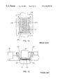
- FIG. 1 is a schematic cross-sectional view showing the pertinent portions of a first embodiment of the semiconductor device testing apparatus according to the present invention
- FIG. 2 is a schematic cross-sectional view showing a modified form of the first embodiment illustrated in FIG. 1;
- FIG. 3 is a schematic cross-sectional view showing an another modified form of the first embodiment illustrated in FIG. 1;
- FIG. 4 is a schematic cross-sectional view showing the pertinent portions of a second embodiment of the semiconductor device testing apparatus according to the present invention.
- FIG. 5 is a plan view of an embodiment of the gold pads mounted in the board of the test head of the semiconductor device testing apparatus according to the present invention.
- FIG. 6 is a schematic side view illustrating the positional relation between the constant temperature chamber of the handler and the semiconductor device testing apparatus according to the present invention with the constant temperature chamber being shown in a cross-sectional view;
- FIG. 7 is a diagrammatical illustration of the general arrangement of an example of the handler of the conventional horizontal transporting type in the form of a flow chart
- FIG. 8 is a perspective view showing an example of the conventional test tray
- FIG. 9 is a perspective view showing the test tray of FIG. 8 having device receiving carriers mounted thereto;
- FIG. 11 is a diagrammatical illustration illustrating the manner in which the semiconductor devices loaded on the test tray of FIG. 8 are tested by the use of the IC sockets shown in FIG. 10;
- FIG. 12 is a schematic cross-sectional view illustrating the electrical connection between a BGA package loaded on the device receiving carrier and an IC socket;
- FIG. 13 is a top plan view of the device receiving carrier shown in FIG. 12;
- FIG. 14 is a schematic cross-sectional view illustrating the electrical connection between a QFP package loaded on the device receiving carrier and an IC socket.
- FIG. 1 shows the pertinent portions of a first embodiment of the IC tester according to the present invention which is applicable when the IC packages placed and supported in IC pockets 101 of a device receiving carrier 100 are BGA packages. It is a schematic cross-sectional view illustrating the electrical connection between a BGA package 40 loaded on the device receiving carrier 100 and a fine conductive wire-embedded plate 110 mounted in the bottom of the device receiving carrier 100 and serving as an IC socket and the electrical connection between the fine conductive wire-embedded plate 110 and electric conductor pads 72 mounted in the board 70 of the test head.
- the ball terminals 41 of the BGA package 40 are all exposed through the undersurface of the device receiving carrier 100 , irrespective of where on the bottom of the BGA package 40 the ball terminals 41 may be disposed, and even if the ball terminals 41 are disposed all over the bottom surface of the BGA package.
- the opening 102 in the bottom of the device receiving carrier 100 is closed by the fine conductive wire-embedded plate 110 .
- the wall of the IC pocket 101 in the device receiving carrier 100 has its lower inner surface undercut to form a thin-walled, downwardly protruding, lower fine conductive wire-embedded plate retaining portion 103 .
- the fine conductive wire-embedded plate retaining portion 103 has a fine conductive wire-embedded plate holding groove formed all around the inner wall surface of the fine conductive wire-embedded plate portion 103 at its root, whereby upon being forced inwardly up through the opening 102 of the IC pocket 101 , the fine conductive wire-embedded plate 110 is caused to fit in and be firmly retained by the fine conductive wire-embedded plate holding groove as it is prevented from being moved upwardly any further by the downwardly facing overhanging surface portion of the inner wall of the IC pocket 101 .
- the fine conductive wire-embedded plate 110 is thus mounted to the bottom of the device receiving carrier 100 and closes the opening 102 .
- the fine conductive wire-embedded plate 110 is made to have the function of the conventional IC socket.
- IC sockets are provided on the device receiving carrier for carrying IC packages thereon rather than on the test head of the IC tester as is the case with the prior art IC tester described above.
- the fine conductive wire-embedded plate 110 comprises an electric insulator plate or sheet, preferably a resilient electric insulator plate or sheet 111 and a multiplicity of fine electrically conductive wires 112 embedded in the insulator plate 111 , the conductive wires extending parallel to each other and without contacting each other through the thickness of the insulator plate with the opposite ends exposed at the outer surfaces of the insulator plate.
- the fine conductive wires 112 are very thin in diameter and arranged at very close intervals on the order of 0.1 mm.
- a resilient rubber plate or sheet is used as the insulator plate 111 , and fine wires made of a metal such as copper, silver, gold or the like is used as the fine conductive wires. Therefore, in the following description the insulator plate 111 will be referred to as a rubber plate and the fine conductive wires will be referred to as fine metal wires.
- each of the ball terminals 41 of the BGA package 40 comes into contact with a minute area portion on the top surface of the fine conductive wire-embedded plate 110 . Since each of the minute area portions contains a plurality of fine metal wires 112 , each ball terminal 41 is electrically extended through the metal wires 112 out to the bottom surface of the fine conductive wire-embedded plate 110 with the ball terminals 41 being electrically insulated from each other.
- the ball terminals 41 will be electrically connected with the conductors provided at the bottom surface of the fine conductive wire-embedded plate 110 with the ball terminals being electrically insulated from each other. It is thus to be appreciated that the fine conductive wire-embedded plate 110 performs the same function as the conventional IC socket with the fine metal wires 112 contained in each of the minute area portions functioning like the socket terminals.
- FIG. 1 illustrates an embodiment in which a pad of good conductor (a gold pad 72 in this example) is provided at the minute area portion on the bottom surface of the fine conductive wire-embedded plate 110 opposing each ball terminal 41 of the BGA package 40 , these gold pads 72 being formed in the surface of the board 70 of the test head. Since the board 70 insulatively support the gold pads 72 functioning like the IC socket terminals, a plurality of gold pads 72 are arrayed in a matrix of four rows (lateral rows) ⁇ eight columns (longitudinal rows) on the test head 90 , just like the IC sockets 60 shown in FIG. 10 and as is seen from FIG. 6 . It is needless to say that the number of gold pads 72 mounted on the test head 90 depends upon the number of ICs that can be tested at a time in one IC tester.
- a pad of good conductor a gold pad 72 in this example
- each board 70 has multi-layered wiring patterns (shown in thick solid lines) formed therein.
- the gold pads 72 formed in the surface of the board 70 are electrically connected with the corresponding wiring patterns which are in turn connected through the test head 90 with the IC tester body. While the gold pad 72 is formed in the shape of small circle or small ellipse so as to conform with the shape of the ball terminal 41 of the BGA package 40 , it may of course be of any other suitable shape.
- Device receiving carriers 100 each having a fine conductive wire-embedded plate 110 mounted in the bottom thereof are attached to a test tray 14 , and then in the loader section 11 , BGA packages 40 housing ICs to be tested are placed and supported in the IC pockets 101 of the respective device receiving carriers 100 . Since the shape and size of the IC pocket 101 are determined according to the shape and size of the IC package as explained hereinbefore, the BGA packages 40 placed in the IC pockets are supported therein in a stable manner with the ball terminals 41 facing downwardly.
- each of the ball terminals 41 of the BGA package 40 is electrically connected through the fine conductive wire-embedded plate 110 with the corresponding gold pad 72 of the board 70 , as shown in FIG. 1 . That is, each ball terminal 41 is put into good electrical connection with the gold pad 72 in contact with the minute area portion on the bottom surface of the fine conductive wire-embedded plate 110 through a plurality of fine metal wires 112 embedded in the minute area portion on the top surface of the fine conductive wire-embedded plate 110 .
- a pusher 80 is mounted above the test head, the arrangement being such that the pusher 80 pushes the associated BGA package 40 in the IC pocket 101 from above down to press the fine conductive wire-embedded plate 110 through the ball terminals 41 .
- the ball terminals 41 of the BGA package 40 are electrically connected with the gold pads 72 of the board 70 through the fine metal wires 112 of the fine conductive wire-embedded plate 110 satisfactorily and with high reliability, even if the ball terminals 41 are disposed all over the bottom surface of the BGA package accompanied naturally by enhancement in the integration level and an increase in the number of lead pins. This allows for conducting the test on ICs in BGA packages consistently and with high reliability without the need for providing IC sockets in the test head as in the prior art.
- the device receiving carrier 100 it is possible to avoid reduction in the mechanical strength of the device receiving carrier 100 because the device receiving carrier is configured to carry and support a BGA package 40 on the fine conductive wire-embedded plate 110 attached to the carrier. Further, the fine conductive wire-embedded plate 110 which performs the function of the IC socket makes it possible to provide an IC tester capable of applying high frequency signals due to a substantial reduction in thickness of the IC socket.
- the device receiving carrier 100 may be replaced outside of the constant temperature chamber 20 because the device receiving carrier is mounted to the test tray 14 which is moved through the IC tester in a circulating manner. This avoids occurrence of a change in the temperature in the constant temperature chamber 20 as well as enhancing the operating simplicity, so that only a short time interruption of the test is required before the testing can be resumed.
- the wall of the IC pocket 101 in the device receiving carrier 100 is formed all around the inner surface with a fine conductive wire-embedded plate holding groove so that the fine conductive wire-embedded plate 110 may be affixed to the bottom of the device receiving carrier 100 by being fitted in the fine conductive wire-embedded plate holding groove, it will be appreciated that essentially the same functional advantages as provided by the first embodiment may be obtained by a modified arrangement in which the fine conductive wire-embedded plate 110 is secured to the undersurface of the device receiving carrier 100 by means of fasteners 63 as illustrated in FIG. 2 .
- the fine conductive wire-embedded plate 110 may easily be secured to or removed from the groove in the lower inner wall surface or the undersurface of the device receiving carrier 100 , so that when the type of the IC package to be tested has been changed, it is only required to replace the fine conductive wire-embedded plate 110 to thereby provide the advantage of further enhancing the operational efficiency.
- the fine conductive wire-embedded plate 110 is affixed to the groove in the lower inner wall surface or the undersurface of the device receiving carrier 100 , it is required to form in the board 70 a recess or through-hole 71 for receiving the lower end portion of the device receiving carrier 100 and through-holes 73 for passing the fasteners 63 in the arrangements of FIGS. 1 and 2, respectively.
- FIG. 3 illustrates another modified form of the first embodiment of FIG. 1 in which the fine conductive wire-embedded plate 110 is secured to the undersurface of the device receiving carrier 100 by means of suitable adhesive.
- suitable adhesive such as epoxy
- FIG. 4 shows the pertinent portions of a second embodiment of the IC tester according to the present invention which is applicable when the IC packages placed and supported in IC pockets 101 of a device receiving carrier 100 are QFP packages. It is a schematic cross-sectional view illustrating the electrical connection between a QFP 45 loaded on the device receiving carrier 100 and a fine conductive wire-embedded plate 110 mounted in the bottom of the device receiving carrier 100 and serving as an IC socket and the electrical connection between the fine conductive wire-embedded plate 110 and gold pads 72 formed on the board 70 of the test head.
- the construction of the device receiving carrier 100 is the same as that of the device receiving carrier shown in FIG. 1 for use with the BGA package 40 except that the shape and size of the IC pocket 101 are determined according to the shape and size of the QFP, the numerals in FIG. 4 correspond to those of FIG. 1 for the elements common to both, and those common elements will not be discussed again unless needed.
- the QFP 45 placed in the IC pocket 101 is supported therein in a stable manner with the terminal pins 46 in contact with the surface of the fine conductive wire-embedded plate 110 , since the shape and size of the IC pocket 101 are determined according to the shape and size of the IC package.
- each of the terminal pins 46 of the QFP 45 is electrically connected through the fine conductive wire-embedded plate 110 with the corresponding gold pad 72 of the board 70 , as shown in FIG. 4 . That is, each terminal pin 46 is put into good electrical connection with the gold pad 72 in contact with the minute area portion on the bottom surface of the fine conductive wire-embedded plate 110 through a plurality of fine metal wires 112 embedded in the minute area portion on the top surface of the fine conductive wire-embedded plate 110 . In this position, the pusher 82 is actuated to push the end portions of the corresponding terminal pins 46 from above down to press the fine conductive wire-embedded plate 110 through the end portions of the terminal pins 46 .
- terminal pins 46 of the QFP 45 are electrically connected with the gold pads 72 of the board 70 through the fine metal wires 112 of the fine conductive wire-embedded plate 110 satisfactorily and with high reliability, whereby the test on ICs in QFPs may be conducted consistently and with high reliability without the need for providing IC sockets on the test head as in the prior art.
- the fine conductive wire-embedded plate 110 which performs the function of the IC socket makes it possible to provide an IC tester capable of applying high frequency signals owing to a substantial reduction in thickness of the wire-embedded plate.
- the device receiving carrier 100 may be replaced outside of the constant temperature chamber 20 because the device receiving carrier is mounted to the test tray 14 which is moved through the IC tester in a circulating manner. This avoids occurrence of a change in the temperature in the constant temperature chamber 20 as well as enhancing the operating simplicity, so that only a short time interruption of the test is required before the testing can be resumed.
- FIG. 5 illustrates a pattern of gold pads 72 formed in the board 70 suitable for use in placing and supporting a TSOP on a device receiving carrier 100 .
- the TSOP is a surface mount type package comprising a thin rectangular package body having lead pins protruding horizontally and parallel to each other from its two opposed sides. While the package is rectangular or square in shape, there are a number of variations in the outer dimensions and the number of lead pins. For this reason, in forming two transversely spaced apart rows of rectangular minute gold pads in the surface of the board 70 , the length of each gold pad row (the length from one end to the other of each row) is chosen to accommodate all of the lead pins of TSOP having the maximum length of lead pin array.
- each gold pad (the length in the right-to-left direction as viewed in the drawing) of each gold pad is made as long as possible.
- the spacing (pitch) between adjacent gold pads in each row is chosen to be equal to or less than the minimum pitch of the lead pins of the TSOP.
- a TSOP 120 having standard outer dimensions will be positioned with respect to the gold pad pattern as shown in FIG. 5 ( a ), so that the lead pins will be put into contact with the individual gold pads 72 at their longitudinal middle portions except for a few gold pads located at the opposite ends of each gold pad row.
- a TSOP 121 having the maximum length of lead pin array it will be positioned with respect to the gold pad pattern as shown in FIG.
- minute circular or elliptical gold pads 72 be formed all over the surface area of the board 70 corresponding to the undersurface area of the maximum size BGA package to accommodate BGA package of all sizes. This eliminates the need to replace the board 70 whenever the type of TSOP to be tested is changed. It is apparent that the gold pads 72 in the surface the board 70 may be substituted for by pads formed of conductor other than gold or by terminal elements.
- test head 90 shown in FIG. 6 is configured to be able to change the electrical connection with respect to the board 70 by replacing the circuit board of the test head base 92 . Accordingly, even if the change of type of TSOP to be tested necessitates changing the electrical connection with respect to the board 70 , it is only required to replace the circuit board of the test head located outside of the constant temperature chamber 20 , which contributes to improving the operational efficiency.
- the device receiving carrier is provided with the fine conductive wire-embedded plate 110 which is made to have the function of the conventional IC socket, whereby the need to provide IC sockets on the test head as was required of the prior art is eliminated. Consequently, there is no need to replace IC sockets on the test head when the type of semiconductor device to be tested is changed.
- the replacement of device receiving carriers and/or fine conductive wire-embedded plates is effected by very easy operations outside of the constant temperature chamber, the interruption of the testing occasioned by the change of the type of semiconductor device to be tested is only a short time, leading to a great reduction in the testing time as well as a significant improvement on the operational easiness.
- the ability of the fine conductive wire-embedded plate to perform the function of the IC socket means that a very thin socket can be provided, which in turn makes it possible to provide an IC tester capable of applying high frequency signals.
- the present invention provides the advantage of insuring that the terminals of the semiconductor device, irrespective of the number of terminals, may be reliably connected with the conductor pads or terminals in the board of the test head, because the device receiving carrier is configured to be supported on the fine conductive wire-embedded plate such that the terminals of the semiconductor device are connected with the conductor pads or terminals in the board through the fine conductive wires embedded in the rubber sheet.
Landscapes
- Engineering & Computer Science (AREA)
- Computer Hardware Design (AREA)
- Microelectronics & Electronic Packaging (AREA)
- Physics & Mathematics (AREA)
- General Physics & Mathematics (AREA)
- Manufacturing & Machinery (AREA)
- Power Engineering (AREA)
- Testing Of Individual Semiconductor Devices (AREA)
Applications Claiming Priority (3)
| Application Number | Priority Date | Filing Date | Title |
|---|---|---|---|
| JP8-211584 | 1996-08-09 | ||
| JP21158496 | 1996-08-09 | ||
| PCT/JP1997/002788 WO1998007041A1 (fr) | 1996-08-09 | 1997-08-08 | Appareil d'essai de dispositifs a semi-conducteur |
Publications (1)
| Publication Number | Publication Date |
|---|---|
| US6320398B1 true US6320398B1 (en) | 2001-11-20 |
Family
ID=16608192
Family Applications (1)
| Application Number | Title | Priority Date | Filing Date |
|---|---|---|---|
| US09/051,419 Expired - Fee Related US6320398B1 (en) | 1996-08-09 | 1997-08-08 | Semiconductor device testing apparatus |
Country Status (7)
| Country | Link |
|---|---|
| US (1) | US6320398B1 (ko) |
| KR (1) | KR100393316B1 (ko) |
| CN (1) | CN1083985C (ko) |
| AU (1) | AU3785097A (ko) |
| MY (1) | MY120128A (ko) |
| TW (1) | TW368603B (ko) |
| WO (1) | WO1998007041A1 (ko) |
Cited By (14)
| Publication number | Priority date | Publication date | Assignee | Title |
|---|---|---|---|---|
| US20030117162A1 (en) * | 2001-12-21 | 2003-06-26 | Watts Stephen M. | Parallel integrated circuit test apparatus and test method |
| US20040174180A1 (en) * | 2002-10-31 | 2004-09-09 | Kentaro Fukushima | Connection unit, a board for mounting a device under test, a probe card and a device interfacing part |
| US20050030007A1 (en) * | 2003-08-06 | 2005-02-10 | Elpida Memory, Inc. | Pusher in an autohandler for pressing a semiconductor device |
| US6897670B2 (en) | 2001-12-21 | 2005-05-24 | Texas Instruments Incorporated | Parallel integrated circuit test apparatus and test method |
| DE102005007593A1 (de) * | 2005-02-18 | 2006-08-24 | Infineon Technologies Ag | Adapter- bzw. Sockel-Vorrichtung zum Testen von Halbleiter-Bauelementen und Verfahren zum Aufnehmen eines Halbleiter-Bauelements in einer Sockel- bzw. Adapter-Vorrichtung |
| US20070210811A1 (en) * | 2006-03-07 | 2007-09-13 | Cojocneanu Christian O | Apparatus and method for testing semiconductor devices |
| US20080012592A1 (en) * | 2006-07-13 | 2008-01-17 | Samsung Electronics Co., Ltd. | Device and method for testing semiconductor packages |
| US20090194872A1 (en) * | 2008-01-31 | 2009-08-06 | Broadcom Corporation | Depopulating integrated circuit package ball locations to enable improved edge clearance in shipping tray |
| US20100141287A1 (en) * | 2007-02-14 | 2010-06-10 | Eles Semiconductor Equipment S.P.A. | Test of electronic devices at package level using test boards without sockets |
| US20100141288A1 (en) * | 2007-02-16 | 2010-06-10 | Eles Semiconductor Equipment S.P.A. | Testing integrated circuits on a wafer using a cartridge with pneumatic locking of the wafer on a probe card |
| US20110001507A1 (en) * | 2009-07-01 | 2011-01-06 | Samsung Electronics Co., Ltd. | Semiconductor device and method of performing electrical test on same |
| FR2958756A1 (fr) * | 2010-04-09 | 2011-10-14 | Eads Europ Aeronautic Defence | Systeme de test d'un composant electronique haute frequence |
| CN102707219A (zh) * | 2012-06-21 | 2012-10-03 | 上海华岭集成电路技术股份有限公司 | 用于半导体器件测试的测试装置 |
| US8466705B1 (en) * | 2012-09-27 | 2013-06-18 | Exatron, Inc. | System and method for analyzing electronic devices having a cab for holding electronic devices |
Families Citing this family (15)
| Publication number | Priority date | Publication date | Assignee | Title |
|---|---|---|---|---|
| US6756800B2 (en) * | 2002-04-16 | 2004-06-29 | Teradyne, Inc. | Semiconductor test system with easily changed interface unit |
| WO2004011952A1 (ja) * | 2002-07-30 | 2004-02-05 | Advantest Corporation | 電子部品試験装置 |
| KR100685223B1 (ko) * | 2003-08-08 | 2007-02-22 | 브레인파워컴퍼니 | 인쇄회로기판의 검사방법 |
| US7208936B2 (en) * | 2004-04-12 | 2007-04-24 | Intel Corporation | Socket lid and test device |
| JP4912080B2 (ja) * | 2006-08-16 | 2012-04-04 | 株式会社アドバンテスト | 電子部品ハンドリング装置およびその運用方法、ならびに試験用トレイおよびプッシャ |
| KR101499574B1 (ko) * | 2010-06-15 | 2015-03-10 | (주)테크윙 | 모듈아이씨 핸들러 및 모듈아이씨 핸들러에서의 로딩방법 |
| JP5414739B2 (ja) | 2011-05-25 | 2014-02-12 | 三菱電機株式会社 | 半導体テスト治具 |
| TWM425277U (en) * | 2011-05-27 | 2012-03-21 | Tek Crown Technology Co Ltd | Testing connector for fast detaching and assembling electrical connection module |
| CN103116119A (zh) * | 2011-11-17 | 2013-05-22 | 上海航天测控通信研究所 | 基于hm276层叠式电子产品的测试台及其测试方法 |
| KR101164116B1 (ko) * | 2012-02-29 | 2012-07-12 | 주식회사 유니테스트 | 번인 테스터용 테스트보드 |
| JPWO2013168196A1 (ja) * | 2012-05-10 | 2015-12-24 | ユニテクノ株式会社 | 半導体搬送テスト治具 |
| CN104576467B (zh) * | 2015-01-05 | 2019-02-15 | 武汉新芯集成电路制造有限公司 | 一种快速装载sop芯片的模具 |
| KR101780935B1 (ko) | 2016-03-30 | 2017-09-27 | 리노공업주식회사 | 검사소켓유니트 |
| CN106483343A (zh) * | 2016-11-03 | 2017-03-08 | 苏州创瑞机电科技有限公司 | 带加热功能的手动直针测试插座 |
| CN113687111B (zh) * | 2021-08-26 | 2024-02-06 | 深圳市佳润芯电子科技有限公司 | 一种能够调节方位坐标的集成电路板测试装置 |
Citations (20)
| Publication number | Priority date | Publication date | Assignee | Title |
|---|---|---|---|---|
| US4252391A (en) * | 1979-06-19 | 1981-02-24 | Shin-Etsu Polymer Co., Ltd. | Anisotropically pressure-sensitive electroconductive composite sheets and method for the preparation thereof |
| US4766371A (en) * | 1982-07-24 | 1988-08-23 | Risho Kogyo Co., Ltd. | Test board for semiconductor packages |
| JPS63236978A (ja) | 1987-03-25 | 1988-10-03 | Nec Kyushu Ltd | 測定用ソケツト |
| US4778950A (en) * | 1985-07-22 | 1988-10-18 | Digital Equipment Corporation | Anisotropic elastomeric interconnecting system |
| US4933747A (en) * | 1989-03-27 | 1990-06-12 | Motorola Inc. | Interconnect and cooling system for a semiconductor device |
| JPH04131773A (ja) | 1990-09-21 | 1992-05-06 | Nec Corp | 電子回路パッケージ接続不良検出方式 |
| JPH04349057A (ja) | 1991-05-27 | 1992-12-03 | Fujitsu Ten Ltd | アンチスキッド制御装置 |
| US5227717A (en) * | 1991-12-03 | 1993-07-13 | Sym-Tek Systems, Inc. | Contact assembly for automatic test handler |
| JPH05288803A (ja) | 1992-04-14 | 1993-11-05 | Fujitsu Ltd | Icトレー |
| US5313156A (en) * | 1991-12-04 | 1994-05-17 | Advantest Corporation | Apparatus for automatic handling |
| US5419710A (en) * | 1994-06-10 | 1995-05-30 | Pfaff; Wayne K. | Mounting apparatus for ball grid array device |
| US5440240A (en) * | 1991-06-04 | 1995-08-08 | Micron Technology, Inc. | Z-axis interconnect for discrete die burn-in for nonpackaged die |
| US5461327A (en) * | 1992-08-31 | 1995-10-24 | Tokyo Electron Limited | Probe apparatus |
| JPH08194032A (ja) | 1995-01-18 | 1996-07-30 | Advantest Corp | Icテスタ用水平搬送型ハンドラ |
| JPH08335486A (ja) | 1995-06-08 | 1996-12-17 | Shin Etsu Polymer Co Ltd | 半導体パッケージ接続用ソケット |
| JPH0933606A (ja) | 1995-07-20 | 1997-02-07 | Shin Etsu Polymer Co Ltd | 半導体素子検査用治具 |
| JPH09102537A (ja) | 1995-10-06 | 1997-04-15 | Nec Corp | 半導体装置用包装部材及びこれを用いた半導体装置のテスト方法 |
| US5800184A (en) * | 1994-03-08 | 1998-09-01 | International Business Machines Corporation | High density electrical interconnect apparatus and method |
| US5966022A (en) * | 1996-11-08 | 1999-10-12 | W. L. Gore & Associates, Inc. | Wafer level burn-in system |
| US6244874B1 (en) * | 1997-09-16 | 2001-06-12 | Yin Leong Tan | Electrical contactor for testing integrated circuit devices |
-
1997
- 1997-08-08 TW TW086111397A patent/TW368603B/zh not_active IP Right Cessation
- 1997-08-08 WO PCT/JP1997/002788 patent/WO1998007041A1/ja active IP Right Grant
- 1997-08-08 CN CN97191059A patent/CN1083985C/zh not_active Expired - Fee Related
- 1997-08-08 US US09/051,419 patent/US6320398B1/en not_active Expired - Fee Related
- 1997-08-08 KR KR10-1998-0702582A patent/KR100393316B1/ko not_active IP Right Cessation
- 1997-08-08 AU AU37850/97A patent/AU3785097A/en not_active Abandoned
- 1997-08-09 MY MYPI97003659A patent/MY120128A/en unknown
Patent Citations (21)
| Publication number | Priority date | Publication date | Assignee | Title |
|---|---|---|---|---|
| US4252391A (en) * | 1979-06-19 | 1981-02-24 | Shin-Etsu Polymer Co., Ltd. | Anisotropically pressure-sensitive electroconductive composite sheets and method for the preparation thereof |
| US4766371A (en) * | 1982-07-24 | 1988-08-23 | Risho Kogyo Co., Ltd. | Test board for semiconductor packages |
| US4778950A (en) * | 1985-07-22 | 1988-10-18 | Digital Equipment Corporation | Anisotropic elastomeric interconnecting system |
| JPS63236978A (ja) | 1987-03-25 | 1988-10-03 | Nec Kyushu Ltd | 測定用ソケツト |
| US4933747A (en) * | 1989-03-27 | 1990-06-12 | Motorola Inc. | Interconnect and cooling system for a semiconductor device |
| JPH04131773A (ja) | 1990-09-21 | 1992-05-06 | Nec Corp | 電子回路パッケージ接続不良検出方式 |
| JPH04349057A (ja) | 1991-05-27 | 1992-12-03 | Fujitsu Ten Ltd | アンチスキッド制御装置 |
| US5440240A (en) * | 1991-06-04 | 1995-08-08 | Micron Technology, Inc. | Z-axis interconnect for discrete die burn-in for nonpackaged die |
| US5227717A (en) * | 1991-12-03 | 1993-07-13 | Sym-Tek Systems, Inc. | Contact assembly for automatic test handler |
| JPH0627192A (ja) | 1991-12-03 | 1994-02-04 | Sym Tek Syst Inc | 自動テストハンドラー用コンタクトアセンブリー |
| US5313156A (en) * | 1991-12-04 | 1994-05-17 | Advantest Corporation | Apparatus for automatic handling |
| JPH05288803A (ja) | 1992-04-14 | 1993-11-05 | Fujitsu Ltd | Icトレー |
| US5461327A (en) * | 1992-08-31 | 1995-10-24 | Tokyo Electron Limited | Probe apparatus |
| US5800184A (en) * | 1994-03-08 | 1998-09-01 | International Business Machines Corporation | High density electrical interconnect apparatus and method |
| US5419710A (en) * | 1994-06-10 | 1995-05-30 | Pfaff; Wayne K. | Mounting apparatus for ball grid array device |
| JPH08194032A (ja) | 1995-01-18 | 1996-07-30 | Advantest Corp | Icテスタ用水平搬送型ハンドラ |
| JPH08335486A (ja) | 1995-06-08 | 1996-12-17 | Shin Etsu Polymer Co Ltd | 半導体パッケージ接続用ソケット |
| JPH0933606A (ja) | 1995-07-20 | 1997-02-07 | Shin Etsu Polymer Co Ltd | 半導体素子検査用治具 |
| JPH09102537A (ja) | 1995-10-06 | 1997-04-15 | Nec Corp | 半導体装置用包装部材及びこれを用いた半導体装置のテスト方法 |
| US5966022A (en) * | 1996-11-08 | 1999-10-12 | W. L. Gore & Associates, Inc. | Wafer level burn-in system |
| US6244874B1 (en) * | 1997-09-16 | 2001-06-12 | Yin Leong Tan | Electrical contactor for testing integrated circuit devices |
Cited By (28)
| Publication number | Priority date | Publication date | Assignee | Title |
|---|---|---|---|---|
| US6897670B2 (en) | 2001-12-21 | 2005-05-24 | Texas Instruments Incorporated | Parallel integrated circuit test apparatus and test method |
| US6731127B2 (en) | 2001-12-21 | 2004-05-04 | Texas Instruments Incorporated | Parallel integrated circuit test apparatus and test method |
| US20030117162A1 (en) * | 2001-12-21 | 2003-06-26 | Watts Stephen M. | Parallel integrated circuit test apparatus and test method |
| US20070024307A1 (en) * | 2002-10-31 | 2007-02-01 | Advantest Corporation | Connection unit, a board for mounting a device under test, a probe card and a device interfacing part |
| US7098680B2 (en) * | 2002-10-31 | 2006-08-29 | Advantest Corp. | Connection unit, a board for mounting a device under test, a probe card and a device interfacing part |
| US20040174180A1 (en) * | 2002-10-31 | 2004-09-09 | Kentaro Fukushima | Connection unit, a board for mounting a device under test, a probe card and a device interfacing part |
| US7791360B2 (en) * | 2002-10-31 | 2010-09-07 | Advantest Corp. | Connection unit, a board for mounting a device under test, a probe card and a device interfacing part |
| US20090160467A1 (en) * | 2002-10-31 | 2009-06-25 | Advantest Corporation | Connection unit, a board for mounting a device under test, a probe card and a device interfacing part |
| US7518379B2 (en) * | 2002-10-31 | 2009-04-14 | Advantest Corp. | Connection unit, a board for mounting a device under test, a probe card and a device interfacing part |
| US20050030007A1 (en) * | 2003-08-06 | 2005-02-10 | Elpida Memory, Inc. | Pusher in an autohandler for pressing a semiconductor device |
| US7119531B2 (en) * | 2003-08-06 | 2006-10-10 | Elpida Memory, Inc. | Pusher in an autohandler for pressing a semiconductor device |
| DE102005007593A1 (de) * | 2005-02-18 | 2006-08-24 | Infineon Technologies Ag | Adapter- bzw. Sockel-Vorrichtung zum Testen von Halbleiter-Bauelementen und Verfahren zum Aufnehmen eines Halbleiter-Bauelements in einer Sockel- bzw. Adapter-Vorrichtung |
| US20060205256A1 (en) * | 2005-02-18 | 2006-09-14 | Holger Hoppe | Adapter or socket device for testing semiconductor devices, and method for incorporating a semiconductor device in a socket or adapter device |
| DE102005007593B4 (de) * | 2005-02-18 | 2008-05-29 | Qimonda Ag | Sockel-Vorrichtung zum Testen von Halbleiter-Bauelementen und Verfahren zum Aufnehmen eines Halbleiter-Bauelements in einer Sockel-Vorrichtung |
| US7528617B2 (en) | 2006-03-07 | 2009-05-05 | Testmetrix, Inc. | Apparatus having a member to receive a tray(s) that holds semiconductor devices for testing |
| US20070210811A1 (en) * | 2006-03-07 | 2007-09-13 | Cojocneanu Christian O | Apparatus and method for testing semiconductor devices |
| US20080012592A1 (en) * | 2006-07-13 | 2008-01-17 | Samsung Electronics Co., Ltd. | Device and method for testing semiconductor packages |
| US8330482B2 (en) * | 2007-02-14 | 2012-12-11 | Eles Semiconductor Equipment S.P.A. | Test of electronic devices at package level using test boards without sockets |
| US20100141287A1 (en) * | 2007-02-14 | 2010-06-10 | Eles Semiconductor Equipment S.P.A. | Test of electronic devices at package level using test boards without sockets |
| US20100141288A1 (en) * | 2007-02-16 | 2010-06-10 | Eles Semiconductor Equipment S.P.A. | Testing integrated circuits on a wafer using a cartridge with pneumatic locking of the wafer on a probe card |
| US8314626B2 (en) | 2007-02-16 | 2012-11-20 | Eles Semiconductor Equipment S.P.A. | Testing integrated circuits on a wafer using a cartridge with pneumatic locking of the wafer on a probe card |
| US20090194872A1 (en) * | 2008-01-31 | 2009-08-06 | Broadcom Corporation | Depopulating integrated circuit package ball locations to enable improved edge clearance in shipping tray |
| US20110001507A1 (en) * | 2009-07-01 | 2011-01-06 | Samsung Electronics Co., Ltd. | Semiconductor device and method of performing electrical test on same |
| US8624619B2 (en) * | 2009-07-01 | 2014-01-07 | Samsung Electronics Co., Ltd. | Semiconductor device and method of performing electrical test on same |
| KR101534487B1 (ko) * | 2009-07-01 | 2015-07-08 | 삼성전자주식회사 | 반도체 소자 및 반도체 소자의 프로브 핀 정렬 검사 방법. |
| FR2958756A1 (fr) * | 2010-04-09 | 2011-10-14 | Eads Europ Aeronautic Defence | Systeme de test d'un composant electronique haute frequence |
| CN102707219A (zh) * | 2012-06-21 | 2012-10-03 | 上海华岭集成电路技术股份有限公司 | 用于半导体器件测试的测试装置 |
| US8466705B1 (en) * | 2012-09-27 | 2013-06-18 | Exatron, Inc. | System and method for analyzing electronic devices having a cab for holding electronic devices |
Also Published As
| Publication number | Publication date |
|---|---|
| CN1198817A (zh) | 1998-11-11 |
| AU3785097A (en) | 1998-03-06 |
| MY120128A (en) | 2005-09-30 |
| WO1998007041A1 (fr) | 1998-02-19 |
| KR19990064101A (ko) | 1999-07-26 |
| CN1083985C (zh) | 2002-05-01 |
| TW368603B (en) | 1999-09-01 |
| KR100393316B1 (ko) | 2003-09-19 |
Similar Documents
| Publication | Publication Date | Title |
|---|---|---|
| US6320398B1 (en) | Semiconductor device testing apparatus | |
| US6476629B1 (en) | In-tray burn-in board for testing integrated circuit devices in situ on processing trays | |
| US6459259B1 (en) | Tester for semiconductor devices and test tray used for the same | |
| US4940935A (en) | Automatic SMD tester | |
| US6489790B1 (en) | Socket including pressure conductive rubber and mesh for testing of ball grid array package | |
| US5180974A (en) | Semiconductor testing and shipping system | |
| US7371078B2 (en) | Insert attachable to an insert magazine of a tray for holding an area array type electronic component to be tested | |
| US5945837A (en) | Interface structure for an integrated circuit device tester | |
| US5635832A (en) | IC carrier for use with an IC handler | |
| JP3376784B2 (ja) | Ic試験装置 | |
| JP2940858B2 (ja) | Ic試験装置 | |
| JPH1098083A (ja) | 検査ソケットおよび電気特性検査装置 | |
| KR19980071417A (ko) | 반도체 디바이스 시험장치 | |
| US4767983A (en) | Test fixture for electronic device packages | |
| GB2376353A (en) | Mounting for high frequency device packages for test and/or burn-in | |
| US7094068B2 (en) | Load board | |
| KR20000042989A (ko) | 번인 테스터용 번인보드 | |
| JPH0192669A (ja) | Ic測定用キャリア | |
| JPH039280A (ja) | Icの検査方法 | |
| TWI398638B (zh) | A method of removing the electronic component, and a control program for carrying out the method | |
| US20020144399A1 (en) | Contact column array template and method of use | |
| JPH02281165A (ja) | 半導体検査装置 | |
| JPH1123650A (ja) | バーンインボード | |
| JP2003014814A (ja) | 半導体装置の試験装置及びそれを用いた試験方法 | |
| JPH02121287A (ja) | 半導体装置用ソケット |
Legal Events
| Date | Code | Title | Description |
|---|---|---|---|
| AS | Assignment |
Owner name: ADVANTEST CORPORATION, JAPAN Free format text: ASSIGNMENT OF ASSIGNORS INTEREST;ASSIGNOR:KOBAYASHI, YOSHIHITO;REEL/FRAME:009232/0400 Effective date: 19980310 Owner name: ADVANTEST CORPORATION, JAPAN Free format text: ASSIGNMENT OF ASSIGNORS INTEREST;ASSIGNOR:ITO, AKIHIKO;REEL/FRAME:009232/0407 Effective date: 19980310 |
|
| FPAY | Fee payment |
Year of fee payment: 4 |
|
| REMI | Maintenance fee reminder mailed | ||
| LAPS | Lapse for failure to pay maintenance fees | ||
| STCH | Information on status: patent discontinuation |
Free format text: PATENT EXPIRED DUE TO NONPAYMENT OF MAINTENANCE FEES UNDER 37 CFR 1.362 |
|
| FP | Lapsed due to failure to pay maintenance fee |
Effective date: 20091120 |