US6247479B1 - Washing/drying process apparatus and washing/drying process method - Google Patents
Washing/drying process apparatus and washing/drying process method Download PDFInfo
- Publication number
- US6247479B1 US6247479B1 US09/084,319 US8431998A US6247479B1 US 6247479 B1 US6247479 B1 US 6247479B1 US 8431998 A US8431998 A US 8431998A US 6247479 B1 US6247479 B1 US 6247479B1
- Authority
- US
- United States
- Prior art keywords
- cup
- substrate
- process fluid
- nozzle
- spin chuck
- Prior art date
- Legal status (The legal status is an assumption and is not a legal conclusion. Google has not performed a legal analysis and makes no representation as to the accuracy of the status listed.)
- Expired - Lifetime
Links
Images


Classifications
-
- H—ELECTRICITY
- H01—ELECTRIC ELEMENTS
- H01L—SEMICONDUCTOR DEVICES NOT COVERED BY CLASS H10
- H01L21/00—Processes or apparatus adapted for the manufacture or treatment of semiconductor or solid state devices or of parts thereof
- H01L21/02—Manufacture or treatment of semiconductor devices or of parts thereof
- H01L21/04—Manufacture or treatment of semiconductor devices or of parts thereof the devices having at least one potential-jump barrier or surface barrier, e.g. PN junction, depletion layer or carrier concentration layer
- H01L21/18—Manufacture or treatment of semiconductor devices or of parts thereof the devices having at least one potential-jump barrier or surface barrier, e.g. PN junction, depletion layer or carrier concentration layer the devices having semiconductor bodies comprising elements of Group IV of the Periodic System or AIIIBV compounds with or without impurities, e.g. doping materials
- H01L21/30—Treatment of semiconductor bodies using processes or apparatus not provided for in groups H01L21/20 - H01L21/26
- H01L21/302—Treatment of semiconductor bodies using processes or apparatus not provided for in groups H01L21/20 - H01L21/26 to change their surface-physical characteristics or shape, e.g. etching, polishing, cutting
- H01L21/304—Mechanical treatment, e.g. grinding, polishing, cutting
-
- H—ELECTRICITY
- H01—ELECTRIC ELEMENTS
- H01L—SEMICONDUCTOR DEVICES NOT COVERED BY CLASS H10
- H01L21/00—Processes or apparatus adapted for the manufacture or treatment of semiconductor or solid state devices or of parts thereof
- H01L21/67—Apparatus specially adapted for handling semiconductor or electric solid state devices during manufacture or treatment thereof; Apparatus specially adapted for handling wafers during manufacture or treatment of semiconductor or electric solid state devices or components ; Apparatus not specifically provided for elsewhere
- H01L21/67005—Apparatus not specifically provided for elsewhere
- H01L21/67011—Apparatus for manufacture or treatment
- H01L21/67017—Apparatus for fluid treatment
- H01L21/67028—Apparatus for fluid treatment for cleaning followed by drying, rinsing, stripping, blasting or the like
-
- B—PERFORMING OPERATIONS; TRANSPORTING
- B08—CLEANING
- B08B—CLEANING IN GENERAL; PREVENTION OF FOULING IN GENERAL
- B08B3/00—Cleaning by methods involving the use or presence of liquid or steam
- B08B3/02—Cleaning by the force of jets or sprays
- B08B3/024—Cleaning by means of spray elements moving over the surface to be cleaned
-
- Y—GENERAL TAGGING OF NEW TECHNOLOGICAL DEVELOPMENTS; GENERAL TAGGING OF CROSS-SECTIONAL TECHNOLOGIES SPANNING OVER SEVERAL SECTIONS OF THE IPC; TECHNICAL SUBJECTS COVERED BY FORMER USPC CROSS-REFERENCE ART COLLECTIONS [XRACs] AND DIGESTS
- Y10—TECHNICAL SUBJECTS COVERED BY FORMER USPC
- Y10S—TECHNICAL SUBJECTS COVERED BY FORMER USPC CROSS-REFERENCE ART COLLECTIONS [XRACs] AND DIGESTS
- Y10S134/00—Cleaning and liquid contact with solids
- Y10S134/902—Semiconductor wafer
Definitions
- the present invention relates to a washing/drying process apparatus and a washing/drying method for chemical-solution-washing, rinsing and drying a surface of a substrate such as a semiconductor wafer or a glass substrate for an LCD.
- a washing/drying process apparatus is used in order to remove a contamination such as particles, organic substances or metal ions from the surface of the substrate.
- An example of the apparatus for washing and drying a semiconductor wafer is a single-wafer-type washing/drying process apparatus for processing wafers one by one within a cup.
- a wafer is rotated, while being held by a spin chuck, and a chemical solution is applied to the surface of the spinning wafer for chemical solution washing. Then, pure water is applied to the washed surface to rinse it. Finally, a dry N 2 gas is applied to dry the wafer surface.
- a chemical solution nozzle, a rinse nozzle and a dry nozzle are provided around the cup. These nozzles are moved between the home position and use position by different drive mechanisms.
- a considerable time is needed for switching from the chemical solution nozzle to the rinse nozzle and from the rinse nozzle to the dry gas nozzle. Consequently, so-called a water mark occurs when liquid drops adhering to the surface of the wafer dry naturally.
- the water mark is a compound of H 2 SiO 3 produced by reaction between oxygen and H2O in the atmosphere and silicon or by precipitation of a very small amount of SiO 2 included in rinse liquid (pure water) on the surface of the silicon wafer. Such a water mark may remain on the wafer surface even after the dry process.
- the waste liquid is recovered from the cup and it is reused after regeneration.
- a recovery/regeneration apparatus for recovering and regenerating the waste liquid is disposed as a unit separated from the chemical solution wash apparatus and at a separate location.
- the conventional apparatus occupies a large area within the clean room.
- the length of the waste liquid recovery circuit (recovery piping) and the regenerated chemical solution return circuit (return piping) increases considerably.
- the bottom surface of the wafer is not uniformly covered with the liquid, and after the process liquid has naturally dropped from the bottom surface of the wafer, the bottom surface of the wafer comes in contact with outside air in the state in which it is wet to some degree.
- a great number of gas-liquid interfaces occur on the bottom surface of the wafer and particles will easily occur at the gas-liquid interfaces. Consequently, particles adhere to the bottom surface of the wafer while the wash process is being performed, and the efficiency of the wash process considerably deteriorates.
- An object of the present invention is to provide a small-sized, simple-structured washing/drying process apparatus and a washing/drying process method capable of washing, rinsing and drying a surface of a substrate with a high through-put without producing a water mark.
- Another object of the invention is to provide a washing/drying process apparatus and a washing/drying process method capable of immediately washing away a chemical solution, etc. on an inner wall of a cup and decreasing the length of a waste liquid recovery circuit and a return circuit.
- Still another object of the invention is to provide a washing/drying process apparatus and a washing/drying process method capable of uniformly processing a lower surface of a substrate.
- a washing/drying process apparatus comprises: a spin chuck for holding a substrate such that a surface thereof to be processed faces upward and for rotating the substrate; a process fluid supply mechanism for selectively supplying one or two or more of a plurality of kinds of process fluids to the surface to be processed of the substrate rotated by the spin chuck, the process fluid supply mechanism having a first nozzle with a discharge port for discharging a process fluid which is in a liquid phase under conditions of room temperature and atmospheric pressure, and a second nozzle with a discharge port for discharging fluid which is in a gas phase under conditions of room temperature and atmospheric pressure; a driving mechanism for simultaneously moving the first and second nozzles to a location above the substrate held by the spin chuck; and a controller for controlling operations of the process liquid supply mechanism and the driving mechanism.
- the washing/drying process apparatus further comprises a nozzle assembly in which the first and second nozzles are integrated, the discharge port of the first nozzle and the discharge port of the second nozzle being adjacent to each other in the nozzle assembly. It is also preferable that the discharge port of the first nozzle and the discharge port of the second nozzle are arranged concentrical at a lower part of the nozzle assembly. It is preferable that the discharge port of the first nozzle and the discharge port of the second nozzle are arranged symmetrical at a lower part of the nozzle assembly.
- the first nozzle has a first discharge port for discharging a chemical solution for chemical washing and a second discharge port for discharging pure water for rinsing
- the second nozzle has a third discharge port for discharging isopropyl alcohol vapor for drying and a fourth discharge port for discharging a dry inert gas for drying.
- a washing/drying process apparatus comprises: a cup having at an upper part thereof an opening for loading and unloading a substrate; a spin chuck for holding and rotating the substrate within the cup; a process fluid supply mechanism having a plurality of nozzles for discharging and supplying a process fluid to the substrate held by the spin chuck; and a relative elevation mechanism for relatively and vertically moving at least one of the cup and the spin chuck, thereby varying a positional relationship between the substrate on the spin chuck and the cup.
- the cup has an over-hang portion projecting inward so as to surround the opening and receiving the process fluid dispersed from the rotating substrate.
- the rinse liquid as second process fluid is indirectly applied to the over-hang portion, and dry N 2 gas as second process fluid is indirectly applied to the over-hand portion. Therefore, the inner wall of the cup is always kept in a clean state.
- the washing/drying process apparatus further comprises: a recovery circuit communicating with a lower part of the cup; a recovery/regeneration tank communicating via the recovery circuit with the cup below the cup, for recovering and regenerating the process fluid exhausted from the cup; and a return circuit for returning the regenerated process fluid from the recovery/regeneration tank to the process fluid supply mechanism.
- the recovery circuit, recovery/regeneration tank, return circuit, cup, spin chuck, and process fluid supply mechanism are arranged within a single unit. Thereby, the length of the recovery circuit and return circuit is decreased, and a temperature variation in chemical solution is prevented.
- the spin chuck has a conical reservoir with a diameter decreasing from a periphery thereof toward a center thereof, the reservoir facing a lower surface of the held substrate, and the apparatus further comprises a third nozzle opening at a lowermost part of the reservoir, the third nozzle supplying a rinse liquid to the reservoir and applying the rinse liquid to the lower surface of the held substrate.
- a method of the invention for chemically washing, rinsing and drying a surface of a substrate in a single apparatus comprises the steps of: (a) holding the substrate and starting spin-rotation of the substrate; (b) supplying a chemical solution to the rotating substrate and subjecting the surface of the substrate to a chemical washing process; (c) supplying a rinse solution to the rotating substrate and subjecting the surface of the substrate to a rinse process; (d) supplying a first dry gas to the rotating substrate and subjecting the surface of the substrate to a dry process; (e) supplying a second dry gas to the rotating substrate and subjecting the surface of the substrate to a final dry process; and (f) stopping the spin-rotation of the substrate and releasing the holding of the substrate.
- the first dry gas along with the second dry gas is supplied to the surface of the substrate.
- the first dry gas contains vapor of isopropyl alcohol
- the second dry gas is an inert gas temperature-controlled at a point higher than a boiling point of isopropyl alcohol.
- the inert gas is, for example, nitrogen gas, argon gas, or helium gas.
- a washing/drying process method of the invention for chemical-washing, rinsing and drying a surface of a substrate in an apparatus comprising a cup having at an upper part thereof an opening for loading/unloading the substrate, a spin chuck for holding and rotating the substrate, a relative elevation means for relatively and vertically moving the spin chuck and the cup, and a process fluid supply mechanism with a nozzle for selectively discharging and supplying one or two or more of a plurality of kinds of process liquids to the substrate, comprises: (A) relatively and vertically moving the cup and the spin chuck by the relative elevation means, setting the opening of the cup at a position lower than the pin chuck, and loading the substrate on the spin chuck; (B) relatively and vertically moving the cup and the spin chuck by the relative elevation means, setting the substrate at a first relative height position relative to the cup, and discharging a liquid-phase first process fluid from the nozzle to the substrate, thereby subjecting the surface of the substrate to a chemical washing process; (C) relatively and
- the liquid-phase second process fluid is supplied to the substrate before setting the substrate at the second relative height position.
- the gas-phase second process fluid along with the gas-phase first process fluid is supplied to the substrate.
- the liquid-phase first process fluid is recovered, regenerated, returned to the process fluid supply mechanism, and resupplied to the substrate from the nozzle.
- the gas-phase first process fluid is recovered, regenerated, returned to the process fluid supply mechanism, and resupplied to the substrate from the nozzle.
- the gas-phase first process fluid contains vapor of isopropyl alcohol
- the gas-phase second dry process fluid is an inert gas temperature-controlled at a point higher than a boiling point of isopropyl alcohol.
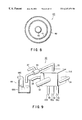
- FIG. 1 is a plan view showing a washing/drying system for washing a surface of a semiconductor wafer with a chemical solution, rising the surface and drying the surface;
- FIG. 2 is a cross-sectional block diagram showing a washing/drying process apparatus according to an embodiment of the present invention
- FIG. 3 is a plan view showing the washing/drying process apparatus according to the embodiment.
- FIG. 4 is a circuit diagram showing a circuit for supplying and recovering a washing chemical solution
- FIG. 5 is a perspective block diagram showing a collective nozzle block (nozzle assembly).
- FIG. 6 is a partially enlarged plan view showing a liquid discharge portion of the collective nozzle block (nozzle assembly);
- FIG. 7 is a partially enlarged plan view showing a modification of the liquid discharge portion of the collective nozzle block (nozzle assembly);
- FIG. 8 is a partially enlarged plan view showing a modification of the liquid discharge portion of the collective nozzle block (nozzle assembly);
- FIG. 9 is a perspective block diagram showing another collective nozzle block (nozzle assembly).
- FIG. 10 is a perspective block diagram showing another collective nozzle block (nozzle assembly).
- FIG. 11 is a partially enlarged plan view showing a liquid discharge portion of the collective nozzle block (nozzle assembly) shown in FIG. 10;
- FIG. 12 is a flow chart illustrating a washing/drying method according to an embodiment of the invention.
- FIG. 13 is a cross-sectional block diagram showing a washing/drying process apparatus according to another embodiment of the invention.
- FIG. 14 is a flow chart illustrating a washing/drying method according to another embodiment of the invention.
- FIGS. 15A to 15 D are see-through cross-sectional views showing various states of the washing/drying apparatus in order to describe the method illustrated in FIG. 14;
- FIG. 16 is a see-through cross-sectional view showing a bottom-surface process apparatus for processing a bottom surface of a substrate.
- FIG. 17 is a plan view showing the upper side of the bottom-surface process apparatus.
- a washing/drying system 1 as shown in FIG. 1, comprises a cassette mount section 2 , a sub-arm mechanism 3 , a process section 4 and a main arm mechanism 5 .
- Four cassettes C each storing 25 wafers W are arranged on the cassette mount section 2 .
- the sub-arm mechanism 3 takes out non-washed wafers W from the cassettes C and transfers them onto the main arm mechanism 5 , or receives washed wafers W from the main arm mechanism 5 and restores them into the cassettes C.
- the process section 4 is provided with a Y-axis transfer path 6 for movement of the main arm mechanism 5 .
- Process units 7 ( 7 A, 7 B), 8 and 9 are successively provided on both sides of the Y-axis transfer path 6 . Specifically, each pair of process units 7 ( 7 A, 7 B), 8 and 9 are opposed to each other, with the transfer path 6 interposed.
- the main arm mechanism 5 comprises a wafer holder, an advancing mechanism for advancing the wafer holder, a Y-axis drive mechanism for driving the wafer holder in the Y-axis direction, a Z-axis drive mechanism for driving the wafer holder in the Z-axis direction, and a ⁇ rotary drive mechanism for rotating the wafer holder about the Z-axis.
- the wafer W is washed with a chemical solution in the first process unit 7 , rinsed and dried. Then the wafer W is washed with another chemical solution in the second process unit 8 , rinsed and dried. At last the wafer W is rinsed with pure water in the third process unit 9 and dried.
- the process unit 7 , 8 , 9 will now be described. Since the process units 7 , 8 and 9 have substantially the same construction, the first process unit 7 will be described representatively.
- the process unit 7 has a casing 7 a , as shown in FIG. 2.
- a spin chuck 10 , a cup 20 and a process fluid supply mechanism 30 are provided within the casing 7 a .
- the spin chuck 10 has a motor 11 , a table 13 and a wafer holder 14 .
- the motor 11 is disposed below the casing 7 a , and its rotary drive shaft 12 is coupled to the lower surface of the table 13 .
- the wafer holder 14 is erected on a peripheral portion of the table 13 and is put in contact with an outer peripheral portion of the wafer W. The wafer W is thus held in the state in which the wafer W is floated above the table 13 .
- a part of the wafer holder 14 is cut out to permit transfer of the wafer W, as shown in FIG. 3 .
- the cup 20 comprises a cylindrical portion 20 a , a bottom portion 20 b , an inner guide portion 20 c , a discharge port 20 d , an upper opening 20 e and an over-hang portion 20 f .
- a space for downward flow of waste liquid is defined between the cylindrical portion 20 a and inner guide portion 20 c .
- a plurality of exhaust ports are formed in the bottom portion 20 b and communicate with exhaust pipes 21 .
- the over-hang portion 20 f is continuous with an upper portion of the cylindrical portion 20 a .
- the upper opening 20 e is surrounded by the over-hang portion 20 f .
- the angle ⁇ between the over-hang portion 20 f and cylindrical portion 20 a is set in a range of from 110° to 135°.
- An atmospheric gas within the cup 20 is exhausted by a vacuum pump (not shown) having a suction port communicating with the bottom of the cup 20 .
- a process liquid separated centrifugally from the wafer W is exhausted to a drain unit 61 via the exhaust pipes 21 opening to the bottom of the cup 20 .
- the drain unit 61 is provided within the single unit casing 7 a along with the spin chuck 10 , cup 20 and process liquid supply mechanism 30 .
- the drain unit 61 comprises a recovery circuit 70 , a tank 71 , a gas-liquid separator 72 , a circulation circuit 80 and a return circuit 33 .
- a chemical solution, pure water, IPA (isopropyl alcohol) vapor and N 2 gas are all exhausted from the cup 20 through the discharge pipes 21 to the drain unit 61 .
- the recovery circuit 70 communicates with the discharge pipes 21 , and the outlet of the recovery circuit 70 communicates with the tank 71 disposed below the cup 20 .
- the gas-liquid separator 72 and drain circuit 73 are arranged successively in this order from above between the recovery circuit 70 and tank 71 .
- the drain circuit 73 communicates with the recovery circuit 70 via an opening/closing valve 74 .
- the gas-liquid separator 72 separates the process fluid coming in from the discharge pipes 21 via the recovery circuit 70 into process liquids, such as chemical solution and pure water, and process gases such as IPA vapor and N 2 gas.
- the gas-liquid separator 72 also eliminates bubbles from the chemical solution.
- the process liquids such as IPA vapor and N 2 gas which are included in the process fluid coming into the gas-liquid separator 72 , are exhausted from an exhaust port 75 provided at an upper portion of the gas-liquid separator 72 , and the process liquids such as chemical solution and pure water are let to flow along an inclined table 76 set in the separator 52 . While the process liquids are flowing, gas components are exhausted from the exhaust port 75 and liquid components are supplied once again into the recovery circuit 70 from an exhaust liquid port 77 provided at a bottom portion of the gas-liquid separator 72 .
- the three-way valve 74 is operated to exhaust the pure water of process liquids separated by the gas-liquid separator, which has been used in the rinse process, to the drain circuit 73 from the recovery circuit 70 .
- the chemical solution of process liquids is received in the tank 71 . Since the tank 71 is provided below the cup 20 , the length of the recovery circuit 70 can be decreased and the used chemical solution can be quickly recovered into the tank 71 by natural drop.
- the circulation circuit 80 for conditioning the chemical solution stored in the tank 71 is connected to the tank 71 .
- the return circuit 33 is connected midway along the circulation circuit 80 via a three-way valve 81 .
- the outlet of the return circuit 33 is connected to the process liquid supply mechanism 30 .
- the chemical solution from the tank 71 which has been conditioned by the circulation circuit 80 , is returned to the nozzle of the supply mechanism 30 .
- the inlet of the circulation circuit 80 is connected to the bottom surface of the tank 71 .
- a pump 83 , a damper 84 , a heater 85 and a filter 86 are successively arranged midway along the circulation circuit 80 .
- the outlet of the circulation circuit 80 is connected to the upper part of the tank 70 .
- the three-way valve 81 may be switched to prevent the chemical solution from flowing to the return circuit 33 and to permit the chemical solution recovered from the recovery circuit 70 into the tank 71 to flow to the circulation circuit 80 .
- the chemical solution coming in the circulation circuit 80 is let to flow successively through the damper 84 , heater 85 and filter 86 by the operation of the pump 83 .
- the chemical solution is temperature-conditioned and purified and then returned to the tank 71 .
- the regenerated chemical solution in the tank 71 is let to flow to the return circuit 33 by switching the three-way valve 81 .
- the chemical solution returned to the nozzle of supply mechanism 30 through the return circuit 33 is reused for the washing process of the wafer W.
- the process fluid supply mechanism 30 comprises a nozzle assembly 31 , a chemical solution supply unit 62 , a pure water supply unit 64 , an N 2 gas supply unit 66 , an IPA vapor generator 68 , and a controller 60 .
- the nozzle assembly 31 is attached to a distal end portion of a horizontal arm 32 . As is shown in FIG. 3, the nozzle assembly 31 is swung about a vertical shaft 50 by means of a drive mechanism 51 between a home position (outside the cup 20 ) and a use position (inside the cup 20 ).
- the respective supply units 62 , 64 , 66 and 68 communicate with the nozzle assembly 31 via line tubes 33 , 34 , 35 and 37 .
- the line tubes 33 , 34 , 35 and 37 are made of fluororesin or stainless steel and are flexible. Flow rate control valves (not shown) of the supply units 62 , 64 , 66 and 68 are controlled by the controller 60 .
- the main body of the nozzle assembly 31 has a rectangular shape.
- the horizontal arm 32 is coupled to one side surface of the assembly 31 .
- the line tubes 33 and 34 are connected to other mutually opposed side surfaces of the assembly 31 .
- the line tube 35 is connected to the top surface of the assembly 31 .
- a collective nozzle member 43 is attached to the bottom surface of the assembly 31 .
- the respective line tubes 33 , 34 and 35 are connected to discharge ports 40 , 41 and 42 of the collective nozzle member 43 via internal passages (not shown).
- the first to third discharge ports 40 , 41 and 42 may be arranged symmetrical, as shown in FIGS. 6 and 7, or may be arranged concentric, as shown in FIG. 8 .
- the first discharge port 40 communicates with the line tube 33 , and the line tube 33 communicates with the chemical solution supply unit 62 .
- the second discharge port 41 communicates with the line tube 34 , and the line tube 34 communicates with the pure water supply unit 64 .
- the third discharge port 42 communicates with the line tube 35 , and the line tube 35 communicates with the IPA vapor generator 68 via a three-way valve 36 .
- the IPA vapor generator 68 comprises a tank 68 a , an N 2 gas source 68 b and a take-in pipe 68 c . If N 2 gas is introduced into IPA liquid in the tank 68 a via the take-in pipe 68 c from the N 2 gas source 68 b , IPA vapor is generated by gas bubbling. The IPA vapor (first dry gas) is discharged from the third discharge port 42 of collective nozzle member 43 through the line tube 35 . One passage of the three-way valve 36 communicates with the line tube 37 .
- Dry N 2 gas (second dry gas) is introduced from another N 2 gas source 66 via the line tube 37 , and the IPA vapor is mixed with the dry N 2 gas in the line tube 35 .
- the mixture of the IPA vapor and dry N 2 gas it is possible to use the IPA vapor alone as dry gas.
- the nozzle assembly 31 is reciprocally moved in a horizontal plane between the home position and use position by the swing mechanism 50 , 51 .
- a receiving cup (not shown) may be provided at the home position of the nozzle assembly 31 so that the discharge ports 40 , 41 and 42 of the collective nozzle member 43 in the wait position may be received in the cup and cleaned.
- FIG. 9 shows a nozzle assembly 31 A according to another embodiment of the invention.
- the nozzle assembly 31 A comprises three separate nozzles 33 a , 34 a and 35 a .
- the nozzles 33 a , 34 a and 35 a are linearly arranged on the lower surface of the nozzle assembly 31 A.
- the discharge port of the first nozzle 33 a communicates with the line tube 33
- the discharge port of the second nozzle 34 a communicates with the line tube 34
- the discharge port of the third nozzle 35 a communicates with the line tube 35 .
- FIGS. 10 and 11 show a nozzle assembly 31 B according to still another embodiment of the invention.
- a collective nozzle member 43 A of nozzle assembly 31 B has four discharge ports 40 , 41 , 42 and 44 .
- the first, second and third discharge ports 40 , 41 and 42 are substantially the same as those in the embodiment shown in FIG. 5, the fourth discharge port 44 is newly added.
- the added fourth discharge port 44 communicates with the N 2 gas supply unit 66 via the line tube 39 and discharges only dry N 2 gas.
- the cassette C is placed on the mount section 2 by means of a transfer robot (not shown).
- the cassette C contains 25 prewashed, non-processed semiconductor wafers W.
- the sub-arm mechanism 3 takes out one of the wafers W from the cassette C, and transfers this wafer W to the main arm mechanism 5 .
- the main arm mechanism 5 carries the wafer W into the first process unit 7 and places it on the table 13 of spin chuck 10 (step S 1 ).
- the spin chuck 10 , cup 20 and nozzle assembly 31 are relatively moved, and the cup 20 and nozzle assembly 31 are positioned relative to the wafer W (step S 2 ).
- the spin chuck 10 is rotated at low speed, and a chemical solution is supplied to the line tube 33 of the nozzle assembly 31 .
- the chemical solution is discharged from the discharge port 40 onto the wafer W, and applied to the upper surface of the wafer W (step S 3 ).
- a mixture solution of ammonia solution and hydrogen peroxide solution for example is used as the chemical solution, thereby eliminating contaminants such as organic substance or particles from the surface of the wafer W.
- the valve of the line tube 33 is closed, and the valve of the line tube 34 is opened. Pure water is supplied to the nozzle assembly 31 , and pure water is discharged from the discharge port 41 onto the wafer W. The chemical-washed surface of the wafer W is thus rinsed (step S 4 ).
- the valve of the line tube 34 is closed to stop the supply of pure water.
- the wafer W is then rotated at high speed, and water is separated and removed from the wafer W by centrifugal force.
- the three-way valve 36 of line tubes 35 and 37 is opened, and a mixture gas (first dry gas) of IPA vapor and N 2 gas is supplied to the nozzle assembly 31 .
- the firs dry gas is applied from the discharge port 42 to the wafer W, thus drying the wafer W (step S 5 ).
- the drying step for the wafer W may be finished in this step S 5 alone. It is preferable, however, to apply dry N 2 gas (second dry gas) to the wafer W in the next step S 6 . Since IPA vapor contains particles of carbon, etc., the particles remaining on the surface of the wafer W are removed by the additional drying step using only N 2 gas, following the drying step using the mixture gas of IPA vapor and N 2 gas.
- the N 2 gas is preheated, even if IPA component remains on the surface of the wafer W, the remaining IPA component can be evaporated and removed by the heat of the N 2 gas. It is preferable that the N 2 gas in this case be preheated at a temperature higher than the boiling point of IPA vapor.
- the surface of the wafer W can be completely dried.
- the nozzle assembly 31 stays at a fixed position above the wafer W.
- the main arm mechanism 5 carries out the wafer W from the first process unit 7 (step S 7 ) and then carries it into the second process unit 8 (step S 8 ).
- the nozzle assembly 31 , spin chuck 10 , and cup 20 are relatively moved, and the nozzle assembly 31 is positioned relative to the wafer W on the table 13 (step S 9 ).
- the spin chuck 10 is rotated at a predetermined speed, and a chemical solution is supplied to the line tube 33 of the nozzle assembly 31 .
- the chemical solution is discharged from the discharge port 40 onto the wafer W, and applied to the upper surface of the wafer W (step S 10 ).
- hydrofluoric acid solution is used as the chemical solution.
- Pure water is supplied to the line tube 34 of nozzle assembly 31 , and pure water is discharged from the discharge port 41 .
- the chemical-washed surface of the wafer W is thus rinsed (step S 11 ).
- the wafer W is rotated at high speed, and liquid is separated and removed from the wafer W by centrifugal force.
- the three-way valve 36 of line tubes 35 and 37 is opened, and a mixture gas (first dry gas) of IPA vapor and N 2 gas is supplied to the nozzle assembly 31 .
- the firs dry gas is applied from the discharge port 42 to the wafer W, thus drying the wafer W (step S 12 ).
- the drying step for the wafer W may be finished in this step S 5 alone. It is preferable, however, to apply dry N 2 gas to the wafer W in the next step S 6 .
- N 2 gas is supplied to the line tube 39 of nozzle assembly 31 , and the N 2 gas is applied from the discharge port 44 to the washed surface of the wafer W, thereby finally drying the washed surface (step S 13 ). If the primary drying step using IPA vapor and the secondary drying step using dry N 2 gas (final drying) are combined, the surface of the wafer W can be completely dried. Thus, impure substances such as organic contaminants and particles on the surface of the wafer W can be removed.
- the main arm mechanism 5 carries out the wafer W from the second process unit 8 (step S 14 ) and then stores the processed wafer W in the cassette C of cassette station 2 (step S 15 ). If the cassette C is filled with processed wafers W, the cassette C along with wafers W is carried to the outside. It is possible to finally wash the wafer W in the process unit 9 using a third chemical solution and then dry it.
- the three processes of chemical solution washing, rinsing and drying can carried out by the single nozzle assembly.
- the step of chemical solution washing and rinsing can be quickly switched to the drying step, and occurrence of so-called water marks (stains due to local oxidation reaction between liquid drops and atmosphere on the wafer surface) can be prevented, and the through-put increased.
- the chemical solution/rinsing process through the drying process can be successively performed, and no water mark is produced.
- much time is needed for the switching from the nozzle for chemical solution/rinsing process to the drying process.
- the operation for switching of the nozzle is not required, and the through-put is greatly increased.
- FIGS. 13, 14 and 15 A to 15 D A description of the parts common to those of the first embodiment is omitted.
- the washing/drying process apparatus of the second embodiment is provided as process unit 7 A in the washing process system 1 shown in FIG. 1 .
- the washing/drying process apparatus 7 A comprises various process fluid supply mechanisms 130 and 131 and drive mechanisms 23 , 148 and 149 .
- the process apparatus 7 A is surrounded by housing panels and formed as unit 7 a .
- a casing 7 b is provided within the unit 7 a
- a spin chuck 10 and a cup 20 are provided within the casing 7 b .
- the spin chuck 10 and cup 20 are the same as described above.
- the first process fluid supply mechanism 130 functions to supply a chemical solution as a first process fluid and pure water as a second process fluid to the wafer W.
- the supply mechanism 130 comprises a first nozzle 128 , a nozzle support member 132 , a chemical solution supply source 102 , pure water supply source 104 , a horizontal arm 138 , a swing mechanism (not shown), and an elevation mechanism 148 .
- the swing mechanism (not shown) functions to swing the horizontal arm 138 in a horizontal plane.
- the swing mechanism 138 is substantially the same as the mechanism 50 , 51 shown in FIG. 2 .
- the elevation mechanism 148 comprises an air cylinder whose air supply source (not shown) is controlled by a controller 160 .
- the elevation mechanism 148 elevates the horizontal arm 138 .
- the nozzle support member 132 is provided at a free end portion of the horizontal arm 138 .
- the first nozzle 128 is attached to a lower part of the nozzle support portion 132 .
- the chemical solution supply source 102 communicates with a line tube 135 via a valve 134 and comprises a plurality of tanks, a mass flow meter, a mixer, and a temperature control mechanism (all not shown).
- the chemical solution supply source 102 supplies a chemical solution as a first process fluid.
- the chemical solution supply source 102 mixes, for example, ammonia solution and hydrogen peroxide solution at a predetermined ratio, controls the temperature of the mixture solution of ammonia and hydrogen peroxide, and supplies the mixture solution to the first nozzle 128 .
- the first process fluid may be, for example, hydrofluoric acid solution.
- the rinse liquid supply source 104 communicates with a line tube 137 via a valve 136 , and comprises a tank, a mass flow meter and a temperature control mechanism (all not shown).
- the rinse liquid supply source 104 supplies a rinse liquid as a second process fluid.
- the supply source 104 controls the temperature of, for example, pure water and supplies it to the first nozzle 128 .
- the line tubes 135 and 137 communicate with a common line tube 33 .
- the common line tube 33 communicates with the first nozzle 128 via an internal passage in the nozzle support member 132 .
- the common line tube 33 communicates with the circulation circuit 80 .
- a chemical solution regenerated by the circulation circuit 80 and recovery tank 71 is fed to the common pipe 33 .
- the second process fluid supply mechanism 131 functions to supply IPA vapor as a first process fluid and dry nitride gas as a second process fluid to the wafer W.
- the supply mechanism 131 comprises a second nozzle 129 , a nozzle support member 140 , an IPA vapor supply source 106 , a dry nitride gas supply source 108 , a horizontal arm 145 , a swing mechanism (not shown), and an elevation mechanism 149 .
- the swing mechanism (not shown) functions to swing the horizontal arm 145 in a horizontal plane and is substantially the same as the mechanism 50 , 51 shown in FIG. 2 .
- the elevation mechanism 149 comprises an air cylinder whose air supply source (not shown) is controlled by the controller 160 .
- the elevation mechanism 149 elevates the horizontal arm 145 .
- the nozzle support member 140 is provided at a free end portion of the horizontal arm 145 .
- the second nozzle 129 is attached to a lower part of the nozzle support portion 140 .
- the IPA vapor supply source 106 communicates with a line tube 142 via a valve 141 , and comprises a plurality of tanks, a mass flow meter, a mixer, and a temperature control mechanism (all not shown).
- the IPA vapor supply source 106 mixes, for example, IPA vapor and dry nitrogen gas at a predetermined ratio, controls the temperature and humidity of the mixture gas, and supplies the mixture gas to the second nozzle 129 . It should be noted that IPA vapor alone may be supplied to the second nozzle 129 .
- the dry nitrogen gas supply source 108 communicates with a line tube 144 via a valve 143 and comprises a tank, a mass flow meter and a temperature/humidity control mechanism (all not shown).
- the dry nitrogen gas supply source 108 controls the temperature and humidity of dry nitrogen gas and supplies it to the second nozzle 129 .
- the opening/closing drive units of the valves 134 , 136 , 141 and 143 are controlled by the controller 160 .
- the elevation mechanism 23 for elevating the cup 20 will now be described.
- the elevation mechanism 23 is provided below the cup 20 .
- the elevation mechanism 23 comprises a motor 24 , a driving pulley 24 a , a timing belt 25 , a driven pulley 26 a , ball nut 26 b and a ball screw 26 c .
- An upper end portion of the ball screw 26 c is rotatably coupled to the lower part of the cup 20 , and a lower end portion of the ball screw 26 c is rotatably coupled to a stationary frame (not shown).
- the ball nut 26 b is engaged the ball screw 26 c and coupled to the driven pulley 26 a .
- the timing belt 25 is passed between the pulleys 24 a and 26 a .
- the operation of the motor 24 is controlled by the controller 160 .
- the elevation mechanism 23 vertically moves the cup 20 such that the level of the opening 20 e varies in a range between an upper position P 1 and a lower position P 2 .
- the cup opening 20 e is located at position P 0 when the cup 20 H indicated by a solid line in FIG. 13 is in the home position.
- the opening 20 e is located at position P 1 when the cup 20 U indicated by an imaginary line in FIG. 13 is in its upper position, and at position P 2 when the cup 20 L indicated by an imaginary line in FIG. 13 is in its lower position.
- first relative height position the position of the wafer W relative to the cup 20 when the cup opening 20 e is at the upper position P 1
- second relative height position the position of the wafer W relative to the cup 20 when the opening 20 e is at the home position P 0 or lower position P 2
- the wafer W is taken out of the cassette C by the sub-arm mechanism 3 , and the wafer W is transferred from the sub-arm mechanism 3 to the main arm mechanism 5 .
- the main arm mechanism 5 carries it to the washing/drying process apparatus 7 .
- the cup 20 is lowered and the cup opening 20 e is located at the lower position P 2 , as shown in FIG. 15A (step S 21 ).
- the shutter (not shown) is opened and the wafer holder of the main arm mechanism 5 is introduced into the casing 7 b .
- the wafer W is placed on the spin chuck 10 (step S 22 ).
- the wafer W is located higher than the cup opening 20 e .
- the wafer holder of the main arm mechanism 5 is retreated from the casing 7 b and the shutter (not shown) is closed.
- the cup 20 is raised and the cup opening 20 e is located at the higher position P 1 , as shown in FIG. 15B (step S 23 ).
- the wafer W is in the “first relative height position” relative to the cup 20 .
- the wafer W is located sufficiently below the cup opening 20 e , and the wafer W is completely surrounded by the cup 20 .
- the nozzle support member 132 is moved so that the nozzle 128 is located above the center of rotation of the wafer W.
- the distance L 1 between the discharge port of first nozzle 128 and the upper surface of the wafer W is set at 10 mm to 15 mm.
- the rotation of the spin chuck 10 is started (step S 24 ), and the discharge of the chemical solution as first process fluid from the first nozzle 128 is started (step S 25 ).
- the chemical solution is spread over the entire upper surface of the wafer W by centrifugal force, and the upper surface of wafer W is uniformly chemically washed.
- the chemical solution is centrifugally separated from the wafer W and applied to the inner wall of the cup 20 .
- the applied chemical solution flows down along the inner wall of the cup 20 .
- the waste liquid (chemical solution) flows from the cup 20 through the exhaust pipe 21 to the recovery circuit 70 shown in FIG. 4.
- a gas component is separated and removed from the waste liquid by the gas-liquid separator 72 .
- the waste liquid is then stored in the tank 72 .
- the waste liquid is circulated from the tank 71 to the circulation circuit 80 by the pump 83 and heated by the heater 85 . Impurities in the waste liquid is then removed by the filter 86 and returned to the tank 71 . Through this circulation, the waste liquid in the tank 71 is purified. The thus regenerated liquid is supplied for reuse to the first nozzle 128 through the return circuit 33 .
- valve 134 is closed and the discharge of chemical solution from the first nozzle 128 is stopped (step S 26 ).
- the rotational speed of the spin chuck 10 is switched from low level to high level and the liquid on the wafer W is centrifugally separated and removed.
- the cup 20 is lowered and the cup opening 20 e is set at the home position P 0 , as shown in FIG. 15C (step S 27 ). At this time, the wafer W is located slightly below the cup opening 20 e (“second relative height position).
- the valve 136 is opened and the discharge of pure water as second process fluid from the first nozzle 128 is started (step S 28 ).
- the pure water is spread over the entire upper surface of the rotating wafer W due to centrifugal force, and the upper surface of the wafer W is uniformly rinsed.
- the pure water centrifugally separated from the wafer W is applied to the over-hang portion 20 f of the cup and flows down from the over-hang portion 20 f .
- the chemical solution on the entire inner wall of the cup 20 is removed. Specifically, the upper surface of the wafer W and the inner wall of the cup 20 are simultaneously rinsed.
- step S 29 the discharge of pure water from the first nozzle 128 is stopped and the first nozzle 128 is retreated from the position above the wafer W (step S 29 ).
- the rotational speed of the spin chuck 10 is switched from the low level to high level and the liquid on the wafer W is centrifugally separated and removed.
- step S 30 the cup 20 is raised and the cup opening 20 e is located at the upper position P 1 , as shown in FIG. 15B (step S 30 ).
- the wafer W is set at the “first relative height position” relative to the cup 20 . Specifically, the wafer W is located sufficiently below the cup opening 20 e and the wafer W is completely surrounded by the cup 20 .
- the nozzle support portion 140 is moved and the second nozzle 129 is located at a point above the center of rotation of the wafer W.
- the second nozzle 129 is approached to the wafer W and the distance L 2 between the discharge port of second nozzle 129 and the upper surface of wafer W is set at 2 mm to 8 mm.
- the discharge of IPA vapor as first process fluid from the second nozzle 129 is started (step S 31 ).
- a predetermined amount of N 2 gas is mixed in the IPA vapor.
- the IPA vapor is spread over the entire upper surface of the wafer W, and water on the upper surface of the wafer W is removed.
- Part of the IPA vapor is liquefied and the liquefied IPA flows down along the inner wall of the cup as waste liquid.
- the waste liquid (IPA liquid) flows through the discharge pipe 21 from the cup 20 to another recovery circuit (not shown).
- a gas component is separated and removed from this waste liquid by another gas-liquid separator (not shown) and stored in another tank (not shown).
- waste liquid IPA liquid
- another circulation circuit not shown
- another pump not shown
- heated by a heater not shown
- passed through a filter not shown
- the waste liquid in the tank is purified through the circulation circuit.
- the thus regenerated liquid is returned to the supply source 106 through another return circuit (not shown) for reuse.
- valve 141 is closed and the discharge of IPA vapor from the second nozzle 128 is stopped (step S 32 ).
- the cup 20 is lowered and the cup opening 20 e is set at the home position P 0 , as shown in FIG. 15C (step S 33 ).
- the wafer W is located slightly lower than the cup opening 20 e (“second relative height position”).
- the valve 143 is opened and the discharge of dry N 2 as second process liquid from the second nozzle 129 is started (step S 34 ).
- the dry N 2 gas is spread over the entire upper surface of the rotating wafer W and thus the upper surface of wafer W is finally dried.
- the dry N 2 gas bounces off the wafer W, hits the over-hang portion 20 f of the cup 20 , and flows down along the inner wall of the cup 20 from the over-hang portion 20 f .
- the entire inner wall of the cup 20 is dried. Specifically, the upper surface of the wafer W and the inner wall of the cup 20 are simultaneously finally dried.
- valve 143 is closed and the discharge of dry N 2 gas from the second nozzle 129 is stopped (step S 35 ). Then, the second nozzle 129 is retreated from the position above the wafer W and the rotation of the wafer W is stopped (step S 36 ).
- step S 37 the cup 20 is lowered and the cup opening 20 e is set at the lower position P 2 , as shown in FIG. 15D (step S 37 ).
- the wafer W is located slightly above the cup opening 20 e .
- the shutter (not shown) is opened and the wafer holder of main arm mechanism 5 is introduced into the casing 7 b .
- the wafer W is taken up from the spin chuck 10 and carried out of the apparatus 7 (step S 38 ).
- the shutter (not shown) is closed, the cup 20 is raised, and the cup opening 20 e is set at the home position P 0 (step S 39 ).
- the wafer W carried out of the process apparatus 7 A is transferred to the next process apparatus 8 .
- a similar washing/drying process is performed.
- the wafer W is finally washed with pure water and dried in the process apparatus 9 .
- the processed wafer W is restored to the cassette C and the wafer W along with the cassette C is carried out of the wash process system 1 .
- the inner wall of the cup 20 including the over-hang portion 20 f is rinsed in real time and dried in real time with the second process fluid (pure water, N 2 gas). Accordingly, the inner wall of the cup 20 is always kept in a clean state. Thus, contamination with particles on the wafer W is effectively prevented.
- the second process fluid pure water, N 2 gas
- the amount of consumed first process fluid (chemical solution, IPA) can be greatly reduced.
- the spin chuck 10 , cup 20 , process fluid supply mechanism 130 , 131 , recovery circuit 50 , tank 51 and return circuit 33 are arranged within single unit 7 a , the length of the recovery circuit 50 and return circuit 33 is decreased and the chemical solution, etc. can be recovered and reused with the area occupied by the single apparatus. Accordingly, the area occupied by the wash process system 1 decreases, the manufacture of semiconductor devices can be facilitated, and the productivity of semiconductor devices is enhanced.
- the system for washing and drying the semiconductor wafer W has been described by way of example.
- the present invention is not limited to this embodiment and is applicable to a washing/drying process system for other substrates such as LCD glass substrates.
- the system for washing/drying the upper surface (circuit pattern formation surface) alone of the semiconductor wafer W has been described by way of example.
- This system may be combined with a bottom-surface process apparatus for washing/drying a bottom surface of the wafer W.
- FIGS. 16 and 17 A description of the parts common to those in the first and second embodiments is omitted.
- the washing/drying process apparatus of the third embodiment is provided as process apparatus 7 B in the wash process system 1 shown in FIG. 1 .
- the washing/drying process apparatus 7 B comprises a cup 20 , a spin chuck 220 , a surface (upper surface) process nozzle 230 and a bottom-surface process nozzle 231 .
- the spin chuck 220 has a table 221 for supporting a peripheral portion of a bottom surface of wafer W.
- An upper surface of the table 221 has a conical shape with a diameter increasing from its center toward its periphery.
- a pool 240 is formed on the upper surface 222 .
- a plurality of pins 23 for guiding and aligning the wafer W are erected on the peripheral portion of the table 221 .
- three sets of aligning pins 223 are disposed at three locations (the total number of pins being nine).
- three notches 224 are formed at peripheral portions of the table 221 for transfer of the wafer W.
- a rotary shaft 225 is attached to the lower surface of the table 221 of spin chuck 220 .
- a pulley 226 is attached to the rotary shaft 225 .
- a torque of a motor 227 is transmitted to the pulley 226 through another pulley 228 and a belt 229 .
- a top-surface process nozzle 230 for applying a chemical solution and a rinsing solution to the upper surface of wafer W is movably provided above the spin chuck 220 .
- the nozzle in the first embodiment or second embodiment may be used for the top-surface process nozzle 230 .
- a bottom-surface process nozzle 231 communicates with an internal passage 232 in the rotary shaft 225 and opens to a lowermost portion of the pool 240 .
- the internal passage 232 communicates with a pure water supply source (not shown). Pure water is supplied to the nozzle 231 through the internal passage 232 and discharged from the nozzle 231 to the pool 240 .
- the discharge port of the nozzle 231 faces a central area of the bottom surface of the wafer W on the table 221 .
- the atmosphere in the cup 20 is exhausted from the bottom of the cup 20 by a vacuum pump (not shown) provided outside.
- the wafer W is placed on the table 221 of spin chuck 220 .
- the spin chuck 220 is rotated at a speed of, e.g. 20 rpm.
- a chemical solution is discharged from the nozzle 230 to the upper surface of wafer W, and pure water is discharged from the nozzle 231 to the lower surface of wafer W.
- the upper surface and lower surface of wafer W are simultaneously processed.
- pure water is supplied from the nozzle 230 to rinse the upper surface of wafer W.
- pure water is jetted from the nozzle 231 to a central area of the lower surface of the rotating wafer W.
- the pure water is uniformly spread by centrifugal force from the center of the lower surface of the wafer toward the periphery thereof.
- the pure water in the pool 240 flows from the center of the pool 240 toward the periphery there of by centrifugal force, and overflows through a gap between the wafer W and table 221 .
- the pure water spattered to the surrounding of the wafer W by centrifugal force flows down along the inner wall of cup 20 and exhausted through discharge pipes 21 . Since pure water is constantly supplied from the nozzle 231 , as described above, fresh pure water is always fed from the center toward the periphery of upper surface 222 of spin chuck 220 .
- the supply of pure water from the nozzle 231 is stopped and the washing process for the lower surface of wafer W is finished. Subsequently, the spin chuck is rotated at higher speed, pure water is removed from the lower surface of wafer W, and the lower surface of wafer W is subjected to a drying process. Not only pure water but also a chemical solution for chemical washing may be applied to the lower surface of wafer W.
Applications Claiming Priority (6)
| Application Number | Priority Date | Filing Date | Title |
|---|---|---|---|
| JP15443597A JPH10335298A (ja) | 1997-05-27 | 1997-05-27 | 処理装置及び処理方法 |
| JP9-154435 | 1997-05-27 | ||
| JP16796797A JP3540550B2 (ja) | 1997-06-09 | 1997-06-09 | 処理装置及び処理方法 |
| JP9-167967 | 1997-06-09 | ||
| JP17778097A JPH1116872A (ja) | 1997-06-19 | 1997-06-19 | 処理装置及び処理方法 |
| JP9-177780 | 1997-06-19 |
Publications (1)
| Publication Number | Publication Date |
|---|---|
| US6247479B1 true US6247479B1 (en) | 2001-06-19 |
Family
ID=27320659
Family Applications (1)
| Application Number | Title | Priority Date | Filing Date |
|---|---|---|---|
| US09/084,319 Expired - Lifetime US6247479B1 (en) | 1997-05-27 | 1998-05-26 | Washing/drying process apparatus and washing/drying process method |
Country Status (3)
| Country | Link |
|---|---|
| US (1) | US6247479B1 (ko) |
| KR (1) | KR100626959B1 (ko) |
| TW (1) | TW402737B (ko) |
Cited By (75)
| Publication number | Priority date | Publication date | Assignee | Title |
|---|---|---|---|---|
| US20010037858A1 (en) * | 2000-05-08 | 2001-11-08 | Hiroki Taniyama | Processing apparatus, processing system and processing method |
| US20020043275A1 (en) * | 2000-10-13 | 2002-04-18 | Seiichiro Okuda | Substrate processing apparatus |
| US20020062840A1 (en) * | 2000-06-26 | 2002-05-30 | Steven Verhaverbeke | Assisted rinsing in a single wafer cleaning process |
| US20030010361A1 (en) * | 2001-07-13 | 2003-01-16 | Boyd John M. | Apparatus and method for controlling galvanic corrosion effects on a single-wafer cleaning system |
| US20030047192A1 (en) * | 2000-12-05 | 2003-03-13 | S.E.S. Company Limited | Single wafer type substrate cleaning method and apparatus |
| US6536454B2 (en) * | 2000-07-07 | 2003-03-25 | Sez Ag | Device for treating a disc-shaped object |
| US20030079764A1 (en) * | 2001-11-01 | 2003-05-01 | Keizo Hirose | Substrate processing apparatus and substrate processing method |
| US6589338B1 (en) * | 1999-12-02 | 2003-07-08 | Tokyo Electron Limited | Device for processing substrate |
| US20030176029A1 (en) * | 2002-03-12 | 2003-09-18 | Dainippon Screen Mfg. Co., Ltd. | Substrate treating apparatus and substrate treating method |
| US20030205253A1 (en) * | 2001-06-22 | 2003-11-06 | S.E.S. Company Limited | Single wafer type substrate cleaning method and apparatus |
| US6669809B2 (en) * | 2000-02-25 | 2003-12-30 | Nec Lcd Technologies, Ltd. | Apparatus for removing a coating film |
| US20040031168A1 (en) * | 2002-05-15 | 2004-02-19 | Takazo Sotojima | Method and apparatus for drying substrate |
| US20040040584A1 (en) * | 2002-08-29 | 2004-03-04 | Dainippon Screen Mfg. Co. Ltd. | Substrate processing apparatus and substrate processing method drying substrate |
| US20040089328A1 (en) * | 2000-11-20 | 2004-05-13 | Dainippon Screen Mfg. Co., Ltd. | Substrate cleaning apparatus |
| US20040115957A1 (en) * | 2002-12-17 | 2004-06-17 | Taiwan Semiconductor Manufacturing Co., Ltd. | Apparatus and method for enhancing wet stripping of photoresist |
| US6752877B2 (en) * | 2001-05-30 | 2004-06-22 | S.E.S. Company Limited | Single wafer type cleaning method and apparatus |
| US20040159344A1 (en) * | 2002-11-11 | 2004-08-19 | Hiatt William M. | Cleaning components for use with programmable material consolidation apparatus and systems |
| US20040179173A1 (en) * | 2003-02-20 | 2004-09-16 | Tokyo Ohka Kogyo Co., Ltd. | Multi-stage type processing apparatus |
| US20040231188A1 (en) * | 2001-06-12 | 2004-11-25 | Lauerhaas Jeffrey M. | Megasonic cleaner and dryer |
| US6832616B2 (en) * | 1999-01-04 | 2004-12-21 | Kabushiki Kaisha Toshiba | Substrate treating apparatus |
| US20050026455A1 (en) * | 2003-05-30 | 2005-02-03 | Satomi Hamada | Substrate processing apparatus and substrate processing method |
| US20050115596A1 (en) * | 2001-11-02 | 2005-06-02 | Dainippon Screen Mfg. Co., Ltd. | Substrate cleaning apparatus and substrate cleaning method |
| US20050124518A1 (en) * | 2001-12-07 | 2005-06-09 | Dainippon Screen Mfg. Co., Ltd. | Substrate treating apparatus |
| US20050145268A1 (en) * | 2002-09-30 | 2005-07-07 | Lam Research Corp. | Substrate meniscus interface and methods for operation |
| US20050199503A1 (en) * | 2004-03-12 | 2005-09-15 | Woodruff Daniel J. | Single workpiece processing chamber |
| US20060046413A1 (en) * | 2004-08-30 | 2006-03-02 | Dainippon Screen Mfg. Co., Ltd. | Substrate processing apparatus and substrate processing method |
| US20060070638A1 (en) * | 1999-01-22 | 2006-04-06 | Aegerter Brian K | Methods and apparatus for rinsing and drying |
| US20060086373A1 (en) * | 2004-10-27 | 2006-04-27 | Park Sang-Oh | Apparatus and method for drying substrates used to manufacture semiconductor devices |
| US20070022948A1 (en) * | 2005-04-01 | 2007-02-01 | Rose Alan D | Compact duct system incorporating moveable and nestable baffles for use in tools used to process microelectronic workpieces with one or more treatment fluids |
| CN1301804C (zh) * | 2003-09-19 | 2007-02-28 | 旺宏电子股份有限公司 | 清洗保养旋转蚀刻机的方法 |
| US20070051389A1 (en) * | 2005-09-02 | 2007-03-08 | Jalal Ashjaee | Method and apparatus for substrate rinsing |
| US20070223342A1 (en) * | 2004-10-12 | 2007-09-27 | Takehiko Orii | Substrate Processing Method and Substrate Processing Apparatus |
| US20070240743A1 (en) * | 2006-02-07 | 2007-10-18 | Toshio Hiroe | Substrate processing apparatus |
| US20070240737A1 (en) * | 2002-09-30 | 2007-10-18 | Lam Research Corporation | Post etch wafer surface cleaning with liquid meniscus |
| WO2007124166A2 (en) * | 2006-04-22 | 2007-11-01 | Gens Timothy H | Devices and methods for drying objects using aerosols |
| US20080008834A1 (en) * | 2006-07-07 | 2008-01-10 | Collins Jimmy D | Barrier structure and nozzle device for use in tools used to process microelectronic workpieces with one or more treatment fluids |
| US20080053489A1 (en) * | 2006-09-06 | 2008-03-06 | Tokyo Electron Limited | Substrate cleaning method |
| US20080070418A1 (en) * | 2006-09-15 | 2008-03-20 | Masahiro Miyagi | Substrate processing apparatus and substrate processing method |
| WO2008041211A2 (en) * | 2006-10-02 | 2008-04-10 | Sez Ag | Device and method for removing liquid from a surface of a disc-like article |
| US20080093340A1 (en) * | 2006-10-06 | 2008-04-24 | Mitsunori Nakamori | Substrate processing method, substrate processing apparatus, and storage medium |
| US20080092813A1 (en) * | 2006-10-23 | 2008-04-24 | Tokyo Electron Limited | Liquid treatment apparatus, mounting and dismounting method of a cup body, and storage medium |
| US7377053B1 (en) * | 2000-01-17 | 2008-05-27 | Daikin Industries, Ltd. | Method and device for drying substrate |
| US20080251148A1 (en) * | 2007-04-16 | 2008-10-16 | Lam Research Corporation | Fluid Handling System for Wafer Electroless Plating and Associated Methods |
| US20080254621A1 (en) * | 2007-04-16 | 2008-10-16 | Lam Research Corporation | Wafer Electroless Plating System and Associated Methods |
| US20080308131A1 (en) * | 2003-10-10 | 2008-12-18 | Semes Co., Ltd. | Method and apparatus for cleaning and driving wafers |
| US20080314870A1 (en) * | 2005-02-07 | 2008-12-25 | Yuki Inoue | Substrate Processing Method, Substrate Processing Apparatus, and Control Program |
| CN100452307C (zh) * | 2005-03-21 | 2009-01-14 | 细美事有限公司 | 清洗和干燥晶片的方法 |
| US20090033898A1 (en) * | 2007-07-30 | 2009-02-05 | Tokyo Electron Limited | Developing apparatus, developing method and storage medium |
| US20090038647A1 (en) * | 2007-08-07 | 2009-02-12 | Dekraker David | Rinsing methodologies for barrier plate and venturi containment systems in tools used to process microelectronic workpieces with one or more treatment fluids, and related apparatuses |
| US20090114248A1 (en) * | 2007-11-05 | 2009-05-07 | Seong-Soo Kim | Substrate treating apparatus and method for treating substrate using the substrate treating apparatus |
| US20090130614A1 (en) * | 2003-12-26 | 2009-05-21 | Tokyo Electron Limited | Development device and development method |
| US20090180089A1 (en) * | 2002-12-10 | 2009-07-16 | Nikon Corporation | Exposure apparatus and method for producing device |
| US20090241995A1 (en) * | 2008-03-31 | 2009-10-01 | Tokyo Electron Limited | Substrate cleaning method and apparatus |
| US20090280235A1 (en) * | 2008-05-09 | 2009-11-12 | Lauerhaas Jeffrey M | Tools and methods for processing microelectronic workpieces using process chamber designs that easily transition between open and closed modes of operation |
| US20100051068A1 (en) * | 2006-11-30 | 2010-03-04 | Atsushi Miyanari | Processing apparatus fluid-processing a process target body |
| US7806989B2 (en) | 2005-06-23 | 2010-10-05 | Tokyo Electron Limited | Substrate processing method and substrate processing apparatus |
| US20120186607A1 (en) * | 2011-01-25 | 2012-07-26 | Tokyo Electron Limited | Liquid treatment apparatus and method |
| US20130174873A1 (en) * | 2012-01-05 | 2013-07-11 | Tokyo Electron Limited | Substrate cleaning method, substrate cleaning apparatus and storage medium for cleaning substrate |
| US20140360540A1 (en) * | 2011-04-18 | 2014-12-11 | Tokyo Electron Limited | Liquid processing apparatus, liquid processing method, and computer-readable recording medium having program stored therein |
| US20150140818A1 (en) * | 2013-11-15 | 2015-05-21 | Taiwan Semiconductor Manufacturing Company, Ltd. | Methods and systems for chemical mechanical polish cleaning |
| US9287110B2 (en) | 2004-06-30 | 2016-03-15 | Lam Research Corporation | Method and apparatus for wafer electroless plating |
| US20160300736A1 (en) * | 2015-04-10 | 2016-10-13 | Kabushiki Kaisha Toshiba | Processing apparatus |
| WO2017004502A1 (en) * | 2015-07-02 | 2017-01-05 | Centrillion Technology Holdings Corporation | Systems and methods to dispense and mix reagents |
| US9673068B2 (en) | 2014-01-15 | 2017-06-06 | SCREEN Holdings Co., Ltd | Apparatus and method for processing substrate with film having porous structure (porous film) formed on surface layer thereof |
| US20180061675A1 (en) * | 2016-08-25 | 2018-03-01 | Semes Co., Ltd. | Substrate treating apparatus and substrate treating method |
| US9947571B2 (en) | 2014-11-14 | 2018-04-17 | Kabushiki Kaisha Toshiba | Processing apparatus, nozzle, and dicing apparatus |
| US10155252B2 (en) * | 2015-04-30 | 2018-12-18 | Taiwan Semiconductor Manufacturing Co., Ltd. | Semiconductor apparatus and washing method |
| US10376888B2 (en) | 2014-07-03 | 2019-08-13 | Centrillion Technology Holdings Corporation | Device for storage and dispensing of reagents |
| CN110230066A (zh) * | 2019-06-06 | 2019-09-13 | 江苏沙钢集团有限公司 | 一种自动酸洗槽及使用方法 |
| US10691020B2 (en) * | 2018-10-25 | 2020-06-23 | Taiwan Semiconductor Manufacturing Company Ltd. | Apparatus for dispensing liquid material and method for fabricating semiconductor device |
| US10864533B2 (en) * | 2017-06-27 | 2020-12-15 | Taiwan Semiconductor Manufacturing Company, Ltd. | Integrated circuit, system for and method of forming an integrated circuit |
| US20210335596A1 (en) * | 2020-04-24 | 2021-10-28 | Semes Co., Ltd. | Substrate treating apparatus and liquid supplying method |
| CN115475794A (zh) * | 2022-10-10 | 2022-12-16 | 安徽光智科技有限公司 | 镜头的清洗方法 |
| US11537047B2 (en) * | 2019-05-21 | 2022-12-27 | Samsung Electronics Co., Ltd. | Spin coater and semiconductor fabrication method for reducing regeneration of photoresist |
| US20230067737A1 (en) * | 2021-08-24 | 2023-03-02 | Deviceeng Co., Ltd | Substrate treatment apparatus having back nozzle assembly |
Families Citing this family (12)
| Publication number | Priority date | Publication date | Assignee | Title |
|---|---|---|---|---|
| TWI467640B (zh) * | 2006-01-18 | 2015-01-01 | Akrion Technologies Inc | 乾燥旋轉基板之系統及方法 |
| US7644512B1 (en) | 2006-01-18 | 2010-01-12 | Akrion, Inc. | Systems and methods for drying a rotating substrate |
| KR100847590B1 (ko) * | 2006-06-19 | 2008-07-21 | 조현찬 | 반도체 장비용 약액 공급 장치, 이를 위한 모니터링 제어장치 및 모니터링이 가능한 반도체 장비용 약액 공급 장치 |
| KR100776282B1 (ko) * | 2006-06-22 | 2007-11-13 | 세메스 주식회사 | 매엽식 기판 처리 장치 및 방법 |
| KR100794588B1 (ko) * | 2006-08-10 | 2008-01-17 | 세메스 주식회사 | 매엽식 기판 처리 장치 및 방법 |
| KR100809591B1 (ko) * | 2006-09-11 | 2008-03-04 | 세메스 주식회사 | 매엽식 기판 세정 방법 |
| KR100864947B1 (ko) * | 2007-04-19 | 2008-10-23 | 세메스 주식회사 | 약액과 가스의 분리가 가능한 기판 처리 장치 |
| KR100892754B1 (ko) * | 2007-11-02 | 2009-04-15 | 세메스 주식회사 | 기판 처리 장치 및 방법 |
| KR100914534B1 (ko) * | 2007-12-26 | 2009-09-02 | 세메스 주식회사 | 기판 처리 장치 및 이의 세정 방법 |
| JP5148465B2 (ja) * | 2008-12-08 | 2013-02-20 | 東京エレクトロン株式会社 | 液処理方法、液処理装置および記憶媒体 |
| KR101381635B1 (ko) * | 2012-09-21 | 2014-04-04 | 청진테크 주식회사 | 세정 장치 |
| CN103811376A (zh) * | 2012-11-09 | 2014-05-21 | 沈阳芯源微电子设备有限公司 | 一种液体喷洒装置 |
Citations (15)
| Publication number | Priority date | Publication date | Assignee | Title |
|---|---|---|---|---|
| US5190065A (en) * | 1991-11-29 | 1993-03-02 | International Business Machines Corporation | Self-contained washing unit for printed circuit boards |
| US5351360A (en) * | 1991-06-06 | 1994-10-04 | Enya Systems, Limited | Cleaning device for a wafer mount plate |
| US5375291A (en) * | 1992-05-18 | 1994-12-27 | Tokyo Electron Limited | Device having brush for scrubbing substrate |
| US5415691A (en) * | 1991-12-20 | 1995-05-16 | Tokyo Ohka Kogyo Co., Ltd. | Solution coating apparatus |
| US5529626A (en) * | 1994-10-24 | 1996-06-25 | Nec Electronics, Inc. | Spincup with a wafer backside deposition reduction apparatus |
| US5591262A (en) * | 1994-03-24 | 1997-01-07 | Tazmo Co., Ltd. | Rotary chemical treater having stationary cleaning fluid nozzle |
| US5688322A (en) * | 1995-05-24 | 1997-11-18 | Tokyo Electron Limited | Apparatus for coating resist on substrate |
| US5695817A (en) * | 1994-08-08 | 1997-12-09 | Tokyo Electron Limited | Method of forming a coating film |
| US5772764A (en) * | 1995-10-13 | 1998-06-30 | Tokyo Electron Limited | Coating apparatus |
| US5826129A (en) * | 1994-06-30 | 1998-10-20 | Tokyo Electron Limited | Substrate processing system |
| US5853961A (en) * | 1995-04-19 | 1998-12-29 | Tokyo Electron Limited | Method of processing substrate and apparatus for processing substrate |
| US5871584A (en) * | 1994-08-03 | 1999-02-16 | Tokyo Electron Limited | Processing apparatus and processing method |
| US5923915A (en) * | 1996-11-11 | 1999-07-13 | Tokyo Electron Limited | Method and apparatus for processing resist |
| US5937223A (en) * | 1996-11-08 | 1999-08-10 | Tokyo Electron Limited | Processing apparatus |
| US5997653A (en) * | 1996-10-07 | 1999-12-07 | Tokyo Electron Limited | Method for washing and drying substrates |
-
1998
- 1998-05-26 TW TW087108185A patent/TW402737B/zh not_active IP Right Cessation
- 1998-05-26 US US09/084,319 patent/US6247479B1/en not_active Expired - Lifetime
- 1998-05-27 KR KR1019980019186A patent/KR100626959B1/ko not_active IP Right Cessation
Patent Citations (16)
| Publication number | Priority date | Publication date | Assignee | Title |
|---|---|---|---|---|
| US5351360A (en) * | 1991-06-06 | 1994-10-04 | Enya Systems, Limited | Cleaning device for a wafer mount plate |
| US5190065A (en) * | 1991-11-29 | 1993-03-02 | International Business Machines Corporation | Self-contained washing unit for printed circuit boards |
| US5415691A (en) * | 1991-12-20 | 1995-05-16 | Tokyo Ohka Kogyo Co., Ltd. | Solution coating apparatus |
| US5375291A (en) * | 1992-05-18 | 1994-12-27 | Tokyo Electron Limited | Device having brush for scrubbing substrate |
| US5591262A (en) * | 1994-03-24 | 1997-01-07 | Tazmo Co., Ltd. | Rotary chemical treater having stationary cleaning fluid nozzle |
| US5826129A (en) * | 1994-06-30 | 1998-10-20 | Tokyo Electron Limited | Substrate processing system |
| US5871584A (en) * | 1994-08-03 | 1999-02-16 | Tokyo Electron Limited | Processing apparatus and processing method |
| US5803970A (en) * | 1994-08-08 | 1998-09-08 | Tokyo Electron Limited | Method of forming a coating film and coating apparatus |
| US5695817A (en) * | 1994-08-08 | 1997-12-09 | Tokyo Electron Limited | Method of forming a coating film |
| US5529626A (en) * | 1994-10-24 | 1996-06-25 | Nec Electronics, Inc. | Spincup with a wafer backside deposition reduction apparatus |
| US5853961A (en) * | 1995-04-19 | 1998-12-29 | Tokyo Electron Limited | Method of processing substrate and apparatus for processing substrate |
| US5688322A (en) * | 1995-05-24 | 1997-11-18 | Tokyo Electron Limited | Apparatus for coating resist on substrate |
| US5772764A (en) * | 1995-10-13 | 1998-06-30 | Tokyo Electron Limited | Coating apparatus |
| US5997653A (en) * | 1996-10-07 | 1999-12-07 | Tokyo Electron Limited | Method for washing and drying substrates |
| US5937223A (en) * | 1996-11-08 | 1999-08-10 | Tokyo Electron Limited | Processing apparatus |
| US5923915A (en) * | 1996-11-11 | 1999-07-13 | Tokyo Electron Limited | Method and apparatus for processing resist |
Cited By (163)
| Publication number | Priority date | Publication date | Assignee | Title |
|---|---|---|---|---|
| US6832616B2 (en) * | 1999-01-04 | 2004-12-21 | Kabushiki Kaisha Toshiba | Substrate treating apparatus |
| US7429537B2 (en) * | 1999-01-22 | 2008-09-30 | Semitool, Inc. | Methods and apparatus for rinsing and drying |
| US20060070638A1 (en) * | 1999-01-22 | 2006-04-06 | Aegerter Brian K | Methods and apparatus for rinsing and drying |
| US6589338B1 (en) * | 1999-12-02 | 2003-07-08 | Tokyo Electron Limited | Device for processing substrate |
| DE10059637B4 (de) * | 1999-12-02 | 2006-07-13 | Tokyo Electron Ltd. | Gerät und Verfahren zur Substratbearbeitung |
| US7377053B1 (en) * | 2000-01-17 | 2008-05-27 | Daikin Industries, Ltd. | Method and device for drying substrate |
| US6669809B2 (en) * | 2000-02-25 | 2003-12-30 | Nec Lcd Technologies, Ltd. | Apparatus for removing a coating film |
| US6827814B2 (en) * | 2000-05-08 | 2004-12-07 | Tokyo Electron Limited | Processing apparatus, processing system and processing method |
| US20010037858A1 (en) * | 2000-05-08 | 2001-11-08 | Hiroki Taniyama | Processing apparatus, processing system and processing method |
| US7021319B2 (en) * | 2000-06-26 | 2006-04-04 | Applied Materials Inc. | Assisted rinsing in a single wafer cleaning process |
| US20020062840A1 (en) * | 2000-06-26 | 2002-05-30 | Steven Verhaverbeke | Assisted rinsing in a single wafer cleaning process |
| US6536454B2 (en) * | 2000-07-07 | 2003-03-25 | Sez Ag | Device for treating a disc-shaped object |
| US6805769B2 (en) * | 2000-10-13 | 2004-10-19 | Dainippon Screen Mfg. Co., Ltd. | Substrate processing apparatus |
| US20020043275A1 (en) * | 2000-10-13 | 2002-04-18 | Seiichiro Okuda | Substrate processing apparatus |
| US6901938B2 (en) * | 2000-11-20 | 2005-06-07 | Dainippon Screen Mfg. Co., Ltd. | Substrate cleaning apparatus |
| US20040089328A1 (en) * | 2000-11-20 | 2004-05-13 | Dainippon Screen Mfg. Co., Ltd. | Substrate cleaning apparatus |
| SG101461A1 (en) * | 2000-12-05 | 2004-01-30 | S E S Company Ltd | Single wafer type substrate cleaning method and apparatus |
| US20030047192A1 (en) * | 2000-12-05 | 2003-03-13 | S.E.S. Company Limited | Single wafer type substrate cleaning method and apparatus |
| US6807974B2 (en) * | 2000-12-05 | 2004-10-26 | S.E.S. Company Limited | Single wafer type substrate cleaning method and apparatus |
| US6792959B2 (en) | 2001-05-30 | 2004-09-21 | S.E.S. Company Limited | Single wafer type cleaning method and apparatus |
| US6752877B2 (en) * | 2001-05-30 | 2004-06-22 | S.E.S. Company Limited | Single wafer type cleaning method and apparatus |
| US20040231188A1 (en) * | 2001-06-12 | 2004-11-25 | Lauerhaas Jeffrey M. | Megasonic cleaner and dryer |
| US20030205253A1 (en) * | 2001-06-22 | 2003-11-06 | S.E.S. Company Limited | Single wafer type substrate cleaning method and apparatus |
| US6824621B2 (en) * | 2001-06-22 | 2004-11-30 | S.E.S. Company Limited | Single wafer type substrate cleaning method and apparatus |
| US6915809B2 (en) | 2001-06-22 | 2005-07-12 | S.E.S. Company Limited | Single wafer type substrate cleaning method and apparatus |
| WO2003007348A2 (en) * | 2001-07-13 | 2003-01-23 | Lam Research Corporation | Apparatus and method for controlling galvanic corrosion effects on a single-wafer cleaning system |
| US20030010361A1 (en) * | 2001-07-13 | 2003-01-16 | Boyd John M. | Apparatus and method for controlling galvanic corrosion effects on a single-wafer cleaning system |
| CN1306565C (zh) * | 2001-07-13 | 2007-03-21 | 拉姆研究公司 | 控制单晶片清洗系统的电化腐蚀效应的设备和方法 |
| US6858091B2 (en) | 2001-07-13 | 2005-02-22 | Lam Research Corporation | Method for controlling galvanic corrosion effects on a single-wafer cleaning system |
| US20050121059A1 (en) * | 2001-07-13 | 2005-06-09 | Lam Research Corporation | Apparatus for controlling galvanic corrosion effects on a single-wafer cleaning system |
| WO2003007348A3 (en) * | 2001-07-13 | 2003-08-21 | Lam Res Corp | Apparatus and method for controlling galvanic corrosion effects on a single-wafer cleaning system |
| US7364626B2 (en) * | 2001-11-01 | 2008-04-29 | Tokyo Electron Limited | Substrate processing apparatus and substrate processing method |
| US20030079764A1 (en) * | 2001-11-01 | 2003-05-01 | Keizo Hirose | Substrate processing apparatus and substrate processing method |
| US7314529B2 (en) * | 2001-11-02 | 2008-01-01 | Dainippon Screen Mfg. Co., Ltd. | Substrate cleaning apparatus and substrate cleaning method |
| US20050115596A1 (en) * | 2001-11-02 | 2005-06-02 | Dainippon Screen Mfg. Co., Ltd. | Substrate cleaning apparatus and substrate cleaning method |
| US20050124518A1 (en) * | 2001-12-07 | 2005-06-09 | Dainippon Screen Mfg. Co., Ltd. | Substrate treating apparatus |
| US20060283485A1 (en) * | 2002-03-12 | 2006-12-21 | Dainippon Screen Mfg. Co., Ltd. | Substrate treating apparatus and substrate treating method |
| US7299810B2 (en) * | 2002-03-12 | 2007-11-27 | Dainippon Screen Mfg. Co., Ltd. | Substrate treating apparatus with circulating and heating mechanism for removal liquid |
| US20030176029A1 (en) * | 2002-03-12 | 2003-09-18 | Dainippon Screen Mfg. Co., Ltd. | Substrate treating apparatus and substrate treating method |
| US20040031168A1 (en) * | 2002-05-15 | 2004-02-19 | Takazo Sotojima | Method and apparatus for drying substrate |
| US6904702B2 (en) * | 2002-05-15 | 2005-06-14 | Toho Kasei, Ltd | Method and apparatus for drying substrate |
| US7811412B2 (en) * | 2002-08-29 | 2010-10-12 | Dainippon Screen Mfg. Co., Ltd. | Substrate processing apparatus and substrate processing method drying substrate |
| US20040040584A1 (en) * | 2002-08-29 | 2004-03-04 | Dainippon Screen Mfg. Co. Ltd. | Substrate processing apparatus and substrate processing method drying substrate |
| US20050145268A1 (en) * | 2002-09-30 | 2005-07-07 | Lam Research Corp. | Substrate meniscus interface and methods for operation |
| US20070240737A1 (en) * | 2002-09-30 | 2007-10-18 | Lam Research Corporation | Post etch wafer surface cleaning with liquid meniscus |
| US7513262B2 (en) * | 2002-09-30 | 2009-04-07 | Lam Research Corporation | Substrate meniscus interface and methods for operation |
| US7597765B2 (en) * | 2002-09-30 | 2009-10-06 | Lam Research Corporation | Post etch wafer surface cleaning with liquid meniscus |
| US20040159344A1 (en) * | 2002-11-11 | 2004-08-19 | Hiatt William M. | Cleaning components for use with programmable material consolidation apparatus and systems |
| US20070157952A1 (en) * | 2002-11-11 | 2007-07-12 | Hiatt William M | Methods for removing and reclaiming unconsolidated material from substrates following fabrication of objects thereon by programmed material consolidation techniques |
| US20040159340A1 (en) * | 2002-11-11 | 2004-08-19 | Hiatt William M. | Methods for removing and reclaiming unconsolidated material from substrates following fabrication of objects thereon by programmed material consolidation techniques |
| US20090180089A1 (en) * | 2002-12-10 | 2009-07-16 | Nikon Corporation | Exposure apparatus and method for producing device |
| US8089611B2 (en) * | 2002-12-10 | 2012-01-03 | Nikon Corporation | Exposure apparatus and method for producing device |
| US20040115957A1 (en) * | 2002-12-17 | 2004-06-17 | Taiwan Semiconductor Manufacturing Co., Ltd. | Apparatus and method for enhancing wet stripping of photoresist |
| US7166184B2 (en) * | 2003-02-20 | 2007-01-23 | Tokyo Ohka Kogyo Co., Ltd. | Multi-stage type processing apparatus |
| US20040179173A1 (en) * | 2003-02-20 | 2004-09-16 | Tokyo Ohka Kogyo Co., Ltd. | Multi-stage type processing apparatus |
| US20100043839A1 (en) * | 2003-05-30 | 2010-02-25 | Satomi Hamada | Substrate processing method |
| US20050026455A1 (en) * | 2003-05-30 | 2005-02-03 | Satomi Hamada | Substrate processing apparatus and substrate processing method |
| CN1301804C (zh) * | 2003-09-19 | 2007-02-28 | 旺宏电子股份有限公司 | 清洗保养旋转蚀刻机的方法 |
| US20080308131A1 (en) * | 2003-10-10 | 2008-12-18 | Semes Co., Ltd. | Method and apparatus for cleaning and driving wafers |
| US20090130614A1 (en) * | 2003-12-26 | 2009-05-21 | Tokyo Electron Limited | Development device and development method |
| US8026048B2 (en) | 2003-12-26 | 2011-09-27 | Tokyo Electron Limited | Developing apparatus and developing method |
| US20100330508A1 (en) * | 2003-12-26 | 2010-12-30 | Tokyo Electron Limited | Developing apparatus and developing method |
| US7823534B2 (en) | 2003-12-26 | 2010-11-02 | Tokyo Electron Limited | Development device and development method |
| US8562752B2 (en) * | 2004-03-12 | 2013-10-22 | Applied Materials, Inc. | Single workpiece processing chamber |
| US20120060869A1 (en) * | 2004-03-12 | 2012-03-15 | Woodruff Daniel J | Single workpiece processing chamber |
| US8118044B2 (en) * | 2004-03-12 | 2012-02-21 | Applied Materials, Inc. | Single workpiece processing chamber with tilting load/unload upper rim |
| US20050199503A1 (en) * | 2004-03-12 | 2005-09-15 | Woodruff Daniel J. | Single workpiece processing chamber |
| CN1722373B (zh) * | 2004-04-01 | 2011-09-28 | 兰姆研究有限公司 | 衬底弯月面界面及用于操作的方法 |
| US9287110B2 (en) | 2004-06-30 | 2016-03-15 | Lam Research Corporation | Method and apparatus for wafer electroless plating |
| US20060046413A1 (en) * | 2004-08-30 | 2006-03-02 | Dainippon Screen Mfg. Co., Ltd. | Substrate processing apparatus and substrate processing method |
| US7789972B2 (en) * | 2004-08-30 | 2010-09-07 | Dainippon Screen Mfg. Co., Ltd. | Substrate processing apparatus and substrate processing method |
| US20090090391A1 (en) * | 2004-08-30 | 2009-04-09 | Dainippon Screen Mfg. Co., Ltd. | Substrate processing apparatus and substrate processing method |
| US8337659B2 (en) * | 2004-10-12 | 2012-12-25 | Tokyo Electron Limited | Substrate processing method and substrate processing apparatus |
| US8794250B2 (en) | 2004-10-12 | 2014-08-05 | Tokyo Electron Limited | Substrate processing method and substrate processing apparatus |
| US20070223342A1 (en) * | 2004-10-12 | 2007-09-27 | Takehiko Orii | Substrate Processing Method and Substrate Processing Apparatus |
| US20060086373A1 (en) * | 2004-10-27 | 2006-04-27 | Park Sang-Oh | Apparatus and method for drying substrates used to manufacture semiconductor devices |
| US20080314870A1 (en) * | 2005-02-07 | 2008-12-25 | Yuki Inoue | Substrate Processing Method, Substrate Processing Apparatus, and Control Program |
| US8211242B2 (en) * | 2005-02-07 | 2012-07-03 | Ebara Corporation | Substrate processing method, substrate processing apparatus, and control program |
| CN100452307C (zh) * | 2005-03-21 | 2009-01-14 | 细美事有限公司 | 清洗和干燥晶片的方法 |
| US8544483B2 (en) | 2005-04-01 | 2013-10-01 | Tel Fsi, Inc. | Barrier structure and nozzle device for use in tools used to process microelectronic workpieces with one or more treatment fluids |
| US8899248B2 (en) | 2005-04-01 | 2014-12-02 | Tel Fsi, Inc. | Barrier structure and nozzle device for use in tools used to process microelectronic workpieces with one or more treatment fluids |
| US20070022948A1 (en) * | 2005-04-01 | 2007-02-01 | Rose Alan D | Compact duct system incorporating moveable and nestable baffles for use in tools used to process microelectronic workpieces with one or more treatment fluids |
| US20070245954A1 (en) * | 2005-04-01 | 2007-10-25 | Collins Jimmy D | Barrier structure and nozzle device for use in tools used to process microelectronic workpieces with one or more treatment fluids |
| US8656936B2 (en) | 2005-04-01 | 2014-02-25 | Tel Fsi, Inc. | Barrier structure and nozzle device for use in tools used to process microelectronic workpieces with one or more treatment fluids |
| US7681581B2 (en) | 2005-04-01 | 2010-03-23 | Fsi International, Inc. | Compact duct system incorporating moveable and nestable baffles for use in tools used to process microelectronic workpieces with one or more treatment fluids |
| US8137478B2 (en) | 2005-06-23 | 2012-03-20 | Tokyo Electron Limited | Substrate processing method and substrate processing apparatus |
| US20100307543A1 (en) * | 2005-06-23 | 2010-12-09 | Tokyo Electron Limited | Substrate processing method and substrate processing apparatus |
| US7806989B2 (en) | 2005-06-23 | 2010-10-05 | Tokyo Electron Limited | Substrate processing method and substrate processing apparatus |
| US20070051389A1 (en) * | 2005-09-02 | 2007-03-08 | Jalal Ashjaee | Method and apparatus for substrate rinsing |
| US20070240743A1 (en) * | 2006-02-07 | 2007-10-18 | Toshio Hiroe | Substrate processing apparatus |
| US7938129B2 (en) * | 2006-02-07 | 2011-05-10 | Dainippon Screen Mfg. Co., Ltd. | Substrate processing apparatus |
| WO2007124166A2 (en) * | 2006-04-22 | 2007-11-01 | Gens Timothy H | Devices and methods for drying objects using aerosols |
| WO2007124166A3 (en) * | 2006-04-22 | 2008-01-17 | Timothy H Gens | Devices and methods for drying objects using aerosols |
| US8668778B2 (en) | 2006-07-07 | 2014-03-11 | Tel Fsi, Inc. | Method of removing liquid from a barrier structure |
| US20080008834A1 (en) * | 2006-07-07 | 2008-01-10 | Collins Jimmy D | Barrier structure and nozzle device for use in tools used to process microelectronic workpieces with one or more treatment fluids |
| US8978675B2 (en) | 2006-07-07 | 2015-03-17 | Tel Fsi, Inc. | Method and apparatus for treating a workpiece with arrays of nozzles |
| US8387635B2 (en) | 2006-07-07 | 2013-03-05 | Tel Fsi, Inc. | Barrier structure and nozzle device for use in tools used to process microelectronic workpieces with one or more treatment fluids |
| US8967167B2 (en) | 2006-07-07 | 2015-03-03 | Tel Fsi, Inc. | Barrier structure and nozzle device for use in tools used to process microelectronic workpieces with one or more treatment fluids |
| US9666456B2 (en) | 2006-07-07 | 2017-05-30 | Tel Fsi, Inc. | Method and apparatus for treating a workpiece with arrays of nozzles |
| US7678199B2 (en) | 2006-09-06 | 2010-03-16 | Tokyo Electron Limited | Substrate cleaning method |
| WO2008030713A1 (en) * | 2006-09-06 | 2008-03-13 | Tokyo Electron Limited | Substrate cleaning method |
| US20080053489A1 (en) * | 2006-09-06 | 2008-03-06 | Tokyo Electron Limited | Substrate cleaning method |
| US10468273B2 (en) | 2006-09-15 | 2019-11-05 | SCREEN Holdings Co., Ltd. | Substrate processing method |
| US9852931B2 (en) | 2006-09-15 | 2017-12-26 | SCREEN Holdings Co., Ltd. | Substrate processing apparatus |
| US8815048B2 (en) * | 2006-09-15 | 2014-08-26 | Dainippon Screen Mfg. Co., Ltd. | Substrate processing apparatus and substrate processing method |
| US10629459B2 (en) | 2006-09-15 | 2020-04-21 | SCREEN Holdings Co., Ltd. | Substrate processing apparatus |
| US20080070418A1 (en) * | 2006-09-15 | 2008-03-20 | Masahiro Miyagi | Substrate processing apparatus and substrate processing method |
| US20110168213A1 (en) * | 2006-10-02 | 2011-07-14 | Sez Ag | Device and method for removing liquid from a surface of a disc-like article |
| WO2008041211A3 (en) * | 2006-10-02 | 2008-08-21 | Sez Ag | Device and method for removing liquid from a surface of a disc-like article |
| WO2008041211A2 (en) * | 2006-10-02 | 2008-04-10 | Sez Ag | Device and method for removing liquid from a surface of a disc-like article |
| US8911561B2 (en) | 2006-10-02 | 2014-12-16 | Lam Research Ag | Device and method for removing liquid from a surface of a disc-like article |
| US20100206338A1 (en) * | 2006-10-02 | 2010-08-19 | Sez Ag | Device and method for removing liquid from a surface of a disc-like article |
| US20080093340A1 (en) * | 2006-10-06 | 2008-04-24 | Mitsunori Nakamori | Substrate processing method, substrate processing apparatus, and storage medium |
| US8043469B2 (en) | 2006-10-06 | 2011-10-25 | Tokyo Electron Limited | Substrate processing method, substrate processing apparatus, and storage medium |
| US7984690B2 (en) * | 2006-10-23 | 2011-07-26 | Tokyo Electron Limited | Liquid treatment apparatus, mounting and dismounting method of a cup body, and storage medium |
| US8354141B2 (en) | 2006-10-23 | 2013-01-15 | Tokyo Electron Limited | Liquid treatment apparatus, mounting and dismounting method of a cup body, and storage medium |
| US20080092813A1 (en) * | 2006-10-23 | 2008-04-24 | Tokyo Electron Limited | Liquid treatment apparatus, mounting and dismounting method of a cup body, and storage medium |
| US20110220216A1 (en) * | 2006-10-23 | 2011-09-15 | Tokyo Electron Limited | Liquid treatment apparatus, mounting and dismounting method of a cup body, and storage medium |
| US20100051068A1 (en) * | 2006-11-30 | 2010-03-04 | Atsushi Miyanari | Processing apparatus fluid-processing a process target body |
| US8720456B2 (en) * | 2006-11-30 | 2014-05-13 | Tokyo Ohka Kogyo Co., Ltd. | Processing apparatus fluid-processing a process target body |
| US8069813B2 (en) | 2007-04-16 | 2011-12-06 | Lam Research Corporation | Wafer electroless plating system and associated methods |
| US8844461B2 (en) * | 2007-04-16 | 2014-09-30 | Lam Research Corporation | Fluid handling system for wafer electroless plating and associated methods |
| US20080254621A1 (en) * | 2007-04-16 | 2008-10-16 | Lam Research Corporation | Wafer Electroless Plating System and Associated Methods |
| US20080251148A1 (en) * | 2007-04-16 | 2008-10-16 | Lam Research Corporation | Fluid Handling System for Wafer Electroless Plating and Associated Methods |
| US7665918B2 (en) * | 2007-07-30 | 2010-02-23 | Tokyo Electron Limited | Developing apparatus, developing method and storage medium |
| US20090033898A1 (en) * | 2007-07-30 | 2009-02-05 | Tokyo Electron Limited | Developing apparatus, developing method and storage medium |
| US20090038647A1 (en) * | 2007-08-07 | 2009-02-12 | Dekraker David | Rinsing methodologies for barrier plate and venturi containment systems in tools used to process microelectronic workpieces with one or more treatment fluids, and related apparatuses |
| US7913706B2 (en) | 2007-08-07 | 2011-03-29 | Fsi International, Inc. | Rinsing methodologies for barrier plate and venturi containment systems in tools used to process microelectronic workpieces with one or more treatment fluids, and related apparatuses |
| US20090114248A1 (en) * | 2007-11-05 | 2009-05-07 | Seong-Soo Kim | Substrate treating apparatus and method for treating substrate using the substrate treating apparatus |
| US20090241995A1 (en) * | 2008-03-31 | 2009-10-01 | Tokyo Electron Limited | Substrate cleaning method and apparatus |
| US20090280235A1 (en) * | 2008-05-09 | 2009-11-12 | Lauerhaas Jeffrey M | Tools and methods for processing microelectronic workpieces using process chamber designs that easily transition between open and closed modes of operation |
| US8684015B2 (en) | 2008-05-09 | 2014-04-01 | Tel Fsi, Inc. | Tools and methods for processing microelectronic workpieces using process chamber designs that easily transition between open and closed modes of operation |
| US8235062B2 (en) | 2008-05-09 | 2012-08-07 | Fsi International, Inc. | Tools and methods for processing microelectronic workpieces using process chamber designs that easily transition between open and closed modes of operation |
| US9039840B2 (en) | 2008-05-09 | 2015-05-26 | Tel Fsi, Inc. | Tools and methods for processing microelectronic workpieces using process chamber designs that easily transition between open and closed modes of operation |
| US20120186607A1 (en) * | 2011-01-25 | 2012-07-26 | Tokyo Electron Limited | Liquid treatment apparatus and method |
| US8607807B2 (en) * | 2011-01-25 | 2013-12-17 | Tokyo Electron Limited | Liquid treatment apparatus and method |
| US9108231B2 (en) * | 2011-04-18 | 2015-08-18 | Tokyo Electron Limited | Liquid processing apparatus, liquid processing method, and computer-readable recording medium having program stored therein |
| US20140360540A1 (en) * | 2011-04-18 | 2014-12-11 | Tokyo Electron Limited | Liquid processing apparatus, liquid processing method, and computer-readable recording medium having program stored therein |
| US9307653B2 (en) * | 2012-01-05 | 2016-04-05 | Tokyo Electron Limited | Substrate cleaning method, substrate cleaning apparatus and storage medium for cleaning substrate |
| US20130174873A1 (en) * | 2012-01-05 | 2013-07-11 | Tokyo Electron Limited | Substrate cleaning method, substrate cleaning apparatus and storage medium for cleaning substrate |
| US11264232B2 (en) | 2013-11-15 | 2022-03-01 | Taiwan Semiconductor Manufacturing Company, Ltd | Methods and systems for chemical mechanical polish cleaning |
| US20150140818A1 (en) * | 2013-11-15 | 2015-05-21 | Taiwan Semiconductor Manufacturing Company, Ltd. | Methods and systems for chemical mechanical polish cleaning |
| US9966281B2 (en) * | 2013-11-15 | 2018-05-08 | Taiwan Semiconductor Manufacturing Company, Ltd. | Methods and systems for chemical mechanical polish cleaning |
| US9673068B2 (en) | 2014-01-15 | 2017-06-06 | SCREEN Holdings Co., Ltd | Apparatus and method for processing substrate with film having porous structure (porous film) formed on surface layer thereof |
| US10376888B2 (en) | 2014-07-03 | 2019-08-13 | Centrillion Technology Holdings Corporation | Device for storage and dispensing of reagents |
| US9947571B2 (en) | 2014-11-14 | 2018-04-17 | Kabushiki Kaisha Toshiba | Processing apparatus, nozzle, and dicing apparatus |
| US10332759B2 (en) * | 2015-04-10 | 2019-06-25 | Kabushiki Kaisha Toshiba | Processing apparatus |
| US20160300736A1 (en) * | 2015-04-10 | 2016-10-13 | Kabushiki Kaisha Toshiba | Processing apparatus |
| US10155252B2 (en) * | 2015-04-30 | 2018-12-18 | Taiwan Semiconductor Manufacturing Co., Ltd. | Semiconductor apparatus and washing method |
| WO2017004502A1 (en) * | 2015-07-02 | 2017-01-05 | Centrillion Technology Holdings Corporation | Systems and methods to dispense and mix reagents |
| US10307724B2 (en) | 2015-07-02 | 2019-06-04 | Centrillion Technology Holdings Corporation | Systems and methods to dispense and mix reagents |
| US10707101B2 (en) * | 2016-08-25 | 2020-07-07 | Semes Co., Ltd. | Substrate treating apparatus and substrate treating method |
| US20180061675A1 (en) * | 2016-08-25 | 2018-03-01 | Semes Co., Ltd. | Substrate treating apparatus and substrate treating method |
| US10864533B2 (en) * | 2017-06-27 | 2020-12-15 | Taiwan Semiconductor Manufacturing Company, Ltd. | Integrated circuit, system for and method of forming an integrated circuit |
| US11642682B2 (en) | 2017-06-27 | 2023-05-09 | Taiwan Semiconductor Manufacturing Company, Ltd. | Pipe design for prevent drip |
| US10691020B2 (en) * | 2018-10-25 | 2020-06-23 | Taiwan Semiconductor Manufacturing Company Ltd. | Apparatus for dispensing liquid material and method for fabricating semiconductor device |
| US11537047B2 (en) * | 2019-05-21 | 2022-12-27 | Samsung Electronics Co., Ltd. | Spin coater and semiconductor fabrication method for reducing regeneration of photoresist |
| CN110230066A (zh) * | 2019-06-06 | 2019-09-13 | 江苏沙钢集团有限公司 | 一种自动酸洗槽及使用方法 |
| CN110230066B (zh) * | 2019-06-06 | 2023-09-15 | 江苏沙钢集团有限公司 | 一种自动酸洗槽及使用方法 |
| US20210335596A1 (en) * | 2020-04-24 | 2021-10-28 | Semes Co., Ltd. | Substrate treating apparatus and liquid supplying method |
| US11664212B2 (en) * | 2020-04-24 | 2023-05-30 | Semes Co., Ltd. | Substrate treating apparatus and liquid supplying method |
| US20230067737A1 (en) * | 2021-08-24 | 2023-03-02 | Deviceeng Co., Ltd | Substrate treatment apparatus having back nozzle assembly |
| CN115475794A (zh) * | 2022-10-10 | 2022-12-16 | 安徽光智科技有限公司 | 镜头的清洗方法 |
Also Published As
| Publication number | Publication date |
|---|---|
| TW402737B (en) | 2000-08-21 |
| KR100626959B1 (ko) | 2007-04-25 |
| KR19980087401A (ko) | 1998-12-05 |
Similar Documents
| Publication | Publication Date | Title |
|---|---|---|
| US6247479B1 (en) | Washing/drying process apparatus and washing/drying process method | |
| TWI709169B (zh) | 基板處理方法及基板處理裝置 | |
| KR100309029B1 (ko) | 세정처리장치 및 세정처리방법 | |
| US6068002A (en) | Cleaning and drying apparatus, wafer processing system and wafer processing method | |
| KR100987537B1 (ko) | 기판처리장치 | |
| US7171973B2 (en) | Substrate processing apparatus | |
| KR20020062703A (ko) | 기판처리장치 및 기판처리방법 | |
| US20030127117A1 (en) | Processing apparatus and processing method | |
| EP1758689A2 (en) | System and method for carrying out liquid and subsequent drying treatments on one or more wafers | |
| KR20190112639A (ko) | 기판 처리 방법 및 기판 처리 장치 | |
| US6668844B2 (en) | Systems and methods for processing workpieces | |
| JP3171822B2 (ja) | 洗浄装置及び洗浄方法 | |
| KR20200083790A (ko) | 기판 처리 장치 및 방법 | |
| JPH10335298A (ja) | 処理装置及び処理方法 | |
| JP4849958B2 (ja) | 基板処理ユニットおよび基板処理方法 | |
| KR20100066366A (ko) | 액처리 방법, 액처리 장치 및 기억 매체 | |
| JPH11145099A (ja) | 基板処理装置 | |
| US20020174882A1 (en) | Substrate processing apparatus and substrate processing method | |
| JPH11330041A (ja) | エッチング液による基板処理装置 | |
| KR20080009838A (ko) | 기판 처리 장치 및 방법 | |
| JP3540550B2 (ja) | 処理装置及び処理方法 | |
| KR100749549B1 (ko) | 기판 처리 장치 및 방법 | |
| TWI839024B (zh) | 基板處理裝置 | |
| US20240118216A1 (en) | Chemical test apparatus and substrate processing apparatus | |
| KR102240493B1 (ko) | 기판 처리 방법 및 기판 처리 장치 |
Legal Events
| Date | Code | Title | Description |
|---|---|---|---|
| AS | Assignment |
Owner name: TOKYO ELECTRON LIMITED, JAPAN Free format text: ASSIGNMENT OF ASSIGNORS INTEREST;ASSIGNORS:TANIYAMA, HIROKI;KAMIKAWA, YUJI;TSURUSAKI, KOTARO;REEL/FRAME:009190/0809 Effective date: 19980513 |
|
| STCF | Information on status: patent grant |
Free format text: PATENTED CASE |
|
| FEPP | Fee payment procedure |
Free format text: PAYOR NUMBER ASSIGNED (ORIGINAL EVENT CODE: ASPN); ENTITY STATUS OF PATENT OWNER: LARGE ENTITY |
|
| FPAY | Fee payment |
Year of fee payment: 4 |
|
| FPAY | Fee payment |
Year of fee payment: 8 |
|
| FPAY | Fee payment |
Year of fee payment: 12 |