US6149047A - Die-bonding machine - Google Patents
Die-bonding machine Download PDFInfo
- Publication number
- US6149047A US6149047A US09/339,029 US33902999A US6149047A US 6149047 A US6149047 A US 6149047A US 33902999 A US33902999 A US 33902999A US 6149047 A US6149047 A US 6149047A
- Authority
- US
- United States
- Prior art keywords
- pellet
- die
- pick
- supporting
- semiconductor
- Prior art date
- Legal status (The legal status is an assumption and is not a legal conclusion. Google has not performed a legal analysis and makes no representation as to the accuracy of the status listed.)
- Expired - Fee Related
Links
Images

Classifications
-
- H—ELECTRICITY
- H01—ELECTRIC ELEMENTS
- H01L—SEMICONDUCTOR DEVICES NOT COVERED BY CLASS H10
- H01L21/00—Processes or apparatus adapted for the manufacture or treatment of semiconductor or solid state devices or of parts thereof
- H01L21/02—Manufacture or treatment of semiconductor devices or of parts thereof
- H01L21/04—Manufacture or treatment of semiconductor devices or of parts thereof the devices having at least one potential-jump barrier or surface barrier, e.g. PN junction, depletion layer or carrier concentration layer
- H01L21/50—Assembly of semiconductor devices using processes or apparatus not provided for in a single one of the subgroups H01L21/06 - H01L21/326, e.g. sealing of a cap to a base of a container
- H01L21/52—Mounting semiconductor bodies in containers
-
- H—ELECTRICITY
- H01—ELECTRIC ELEMENTS
- H01L—SEMICONDUCTOR DEVICES NOT COVERED BY CLASS H10
- H01L21/00—Processes or apparatus adapted for the manufacture or treatment of semiconductor or solid state devices or of parts thereof
- H01L21/67—Apparatus specially adapted for handling semiconductor or electric solid state devices during manufacture or treatment thereof; Apparatus specially adapted for handling wafers during manufacture or treatment of semiconductor or electric solid state devices or components ; Apparatus not specifically provided for elsewhere
- H01L21/67005—Apparatus not specifically provided for elsewhere
- H01L21/67011—Apparatus for manufacture or treatment
- H01L21/67144—Apparatus for mounting on conductive members, e.g. leadframes or conductors on insulating substrates
-
- H—ELECTRICITY
- H01—ELECTRIC ELEMENTS
- H01L—SEMICONDUCTOR DEVICES NOT COVERED BY CLASS H10
- H01L21/00—Processes or apparatus adapted for the manufacture or treatment of semiconductor or solid state devices or of parts thereof
- H01L21/67—Apparatus specially adapted for handling semiconductor or electric solid state devices during manufacture or treatment thereof; Apparatus specially adapted for handling wafers during manufacture or treatment of semiconductor or electric solid state devices or components ; Apparatus not specifically provided for elsewhere
- H01L21/68—Apparatus specially adapted for handling semiconductor or electric solid state devices during manufacture or treatment thereof; Apparatus specially adapted for handling wafers during manufacture or treatment of semiconductor or electric solid state devices or components ; Apparatus not specifically provided for elsewhere for positioning, orientation or alignment
- H01L21/681—Apparatus specially adapted for handling semiconductor or electric solid state devices during manufacture or treatment thereof; Apparatus specially adapted for handling wafers during manufacture or treatment of semiconductor or electric solid state devices or components ; Apparatus not specifically provided for elsewhere for positioning, orientation or alignment using optical controlling means
Definitions
- the present invention relates to a die-bonding machine used in fabricating a semiconductor device.
- a semiconductor device is fabricated by sequentially assembling a semiconductor pellet (simply called a "pellet” hereinafter) on a pellet mounting section (called a “land” hereinafter) of a supporting member such as a lead frame or a BGA (ball grid array) board, by means of a die-bonding machine.
- a semiconductor pellet simply called a "pellet” hereinafter
- a pellet mounting section called a “land” hereinafter
- BGA ball grid array
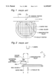
- FIG. 1 is a diagrammatic partial plan view illustrating the relation between a semiconductor wafer and a mechanism for feeding a supporting member such as a lead frame
- FIG. 2 is a diagrammatic side sectional view of the mechanism shown in FIG. 1.
- the supporting member 1 such as the lead frame, having a land on which the pellet is to be mounted and on which a bonding agent such as a solder or a silver (Ag) paste was placed in a preceding step, is loaded on a rail 2, and intermittently fed and then stopped in a left-to-right direction in FIG. 1 (namely, in an X direction) by a feeding mechanism (not shown) so that the land is placed at a predetermined bonding position BP.
- a bonding agent such as a solder or a silver (Ag) paste
- a number of pellets 3 obtained by dicing a wafer are adhered on a sheet (not shown) to maintain a geometrical arrangement before the wafer is divided into the pellets, and the sheet is fixed to a wafer ring 5.
- the wafer ring 5 is fitted into and held by a ring holder 6, which is supported by a supporting and displacing mechanism (not shown).
- This supporting and displacing mechanism can freely displace the ring holder 6 (and hence the pellets 3 adhered on the sheet) in the X direction and in a Y direction perpendicular to the X direction, and also can freely rotate the ring holder 6 (namely, it can displace in an angular direction (a ⁇ direction)), so that a designated pellet is sequentially placed in a fixed pick-up position PP one by one.
- This fixed pick-up position PP is determined to be as near to the bonding position BP as possible, in the Y direction from the bonding position BP.
- a camera 7 is located and fixed directly above the fixed pick-up position PP, and an image of the pellet located on the fixed pick-up position PP, is photographed by the camera 7 and processed by a processing system (not shown) to ascertain whether or not a bad mark exists, and whether or not an appearance abnormality such as a crack or a chipping exists, and also to confirm that the pellet is positioned in place on the fixed pick-up position PP. If the pellet photographed by the camera 7 was defective, the ring holder 6 is displaced by the supporting and displacing mechanism so that a next pellet is moved to the fixed pick-up position PP.
- the ring holder 6 is finely displaced by the supporting and displacing mechanism so that the next pellet is positioned precisely on the fixed pick-up position PP.
- a push-up pin 8 is provided under the ring holder 6, in substantial alignment with the camera 7 in a vertical line.
- the die-bonding machine also includes a pick-up collet having a vacuum nozzle 4 provided at a lower tip end.
- the pick-up collet can be moved so that the vacuum nozzle 4 can be displaced in a vertical direction (namely, in a Z direction) and also in the Y direction, shown by a dotted line in FIG. 2.
- the ring holder 6 is finely displaced by the supporting and displacing mechanism so that the pellet is positioned precisely on the fixed pick-up position PP.
- the vacuum nozzle 4 is displaced to suction up the pellet, and on the other hand, the push-up pin 8 is elevated to push up the pellet and to peel off the pellet from the adhering sheet fixed by the wafer ring 5.
- the vacuum nozzle 4 is lifted up, and moved in the Y direction to a position directly above the bonding position BP, and then, is lowered so that the pellet sucked and held by the vacuum nozzle 4 is placed on the land of the supporting member 1. Thereafter, the vacuum nozzle 4 is released and then lifted up.
- the non-defective pellet is placed on the land of the supporting member 1.
- the bonding position BP and the fixed pick-up position PP are located as near to each other as possible, so that the time for carrying the pellet 3 is shortened, with the result that a high speed die-bonding operation can be realized.
- a moving range of the ring holder 6 becomes a double of the diameter of the wafer, so that the machine becomes large in size.
- the wafer diameter has become 8 inches or 12 inches, this problem has become even worse.
- JP-A-01-152634 (an English abstract of which is available and the content of the English abstract is incorporated by reference in its entirety into this application) proposes a die-bonding machine, which is so configured to imaginarily divide a number of pellets held by the ring holder into four quadrants by two orthogonal straight lines, and to limit the moving range of the ring holder in the X and Y directions to the degree that the pellets included in only one quadrant can be placed on the fixed pick-up position, and on the other hand to rotate the ring holder by 90 degrees at each time the pick-up operation for one quadrant is completed, so that the pick-up operation is carried out quadrant by quadrant.
- the moving range of the ring holder in the X and Y directions can be reduced to one and a half times the diameter of the wafer. Therefore, even the time for rotating the ring holder becomes wasteful, since all the other operations can be sped up, the die-bonding operation can be sped up in total.
- the vacuum suction nozzle of the pellet picking-up and carrying mechanism is constructed to be rotatable so as to adjust the direction of the picked-up pellet in the course of carrying the picked-up pellet, or alternatively, a rotatable relay stage is provided and the pellet picking-up and carrying mechanism is controlled to carry the picked-up pellet to the rotatable relay stage so that the pellet put on the rotatable relay stage is rotated together with the rotatable relay stage to adjust the direction of the pellet and the direction-adjusted pellet is picked up by another vacuum nozzle and carried and located on the land of the supporting member by the second vacuum nozzle.
- Japanese Patent Application Pre-examination Publication No. JP-A-04-111330 proposes another die-bonding machine which does not have the fixed pick-up position.
- the ring holder is rotatable about its center axis (namely, displaceable in the ⁇ direction), but the position of the center axis is fixed both in the X direction and in the Y direction.
- the rotating operation of the ring holder is only for aligning the direction of each pellet, but when each pellet is picked up, the ring holder is not rotated.
- the camera is displaceable both in the X direction and in the Y direction, as to sequentially ascertain the defective/non-defective of the pellet and the position of the pellet.
- the vacuum suction nozzle of the pellet picking-up and carrying mechanism is movable all in the X direction, in the Y direction and in the Z direction to move to the pellet which was ascertained by the camera, to pick up the same pellet, to move in the X direction and in the Y direction so as to locate the picked-up pellet on a predetermined location.
- This Japanese patent publication has no description concerning the push-up pin, but if the push-up pin is provided, the push-up pin is required to move both in the X direction and in the Y direction to follow the displacement of the camera.
- the second prior art die-bonding machine since the ring holder is fixed in the X direction and in the Y direction, and the moving range of the pellet suction nozzle of the pellet picking-up and carrying mechanism is substantially within the ring holder, the machine becomes smaller in size. However, since the pellet picking-up and carrying mechanism has to go to a remote position for picking up the pellet, the die-bonding operation becomes slow. Therefore, it is supposed that the second prior art die-bonding machine can be applied in only the case that a high speed die-bonding operation is not required because a step before the die-bonding step and a step after the die-bonding step in an in-line production line need a substantial time.
- the second prior art die-bonding machine can be applied.
- the die-bonding is carried out at a speed comparable to that of the wiring bonding, the second prior art die-bonding machine can be applied.
- the second prior art die-bonding machine remarkably lowers the die-bonding speed, the second prior art die-bonding machine cannot be applied generally.
- Another object of the present invention is to provide a die-bonding machine having a relatively small size and a satisfactory die-bonding speed, by limiting the moving range of the ring holder to some degree and by fixing the pellet picking-up direction so that the pellet can be picked up by repeating the same movement and therefore control software becomes simple.
- a die-bonding machine for picking up a number of semiconductor pellets arranged in the form of a pellet array, one by one, to place a picked-up semiconductor pellet on a predetermined position, the die-bonding machine comprising:
- a pellet supporting and displacing mechanism for supporting the number of semiconductor pellets arranged in the form of the pellet array, and for displacing the number of semiconductor pellets arranged in the form of the pellet array, in an X direction and in a Y direction;
- a pellet picking-up and carrying mechanism having a pellet sucking means which can be displaced in the X direction, in the Y direction and in a X direction, for picking up one semiconductor pellet positioned on a pick-up position, from the number of semiconductor pellets supported by the pellet supporting and displacing mechanism, and for placing the picked-up semiconductor pellet on the predetermined position, the pick-up position being movable only in the X direction,
- an estimated X-direction coordinate position of the semiconductor pellet to be picked up in relation to the pellet supporting and displacing mechanism is assumed as being "x"
- the pellet supporting and displacing mechanism and the pellet picking-up and carrying mechanism are displaced so that an X-direction coordinate position PX of the pick-up position takes a position expressed by the following equation (1) and an X-direction coordinate position CX of the center point of the pellet supporting and displacing mechanism takes a position expressed by the following equation (2):
- a die-bonding machine for picking up a number of semiconductor pellets arranged in the form of a pellet array, one by one, to place a picked-up semiconductor pellet on a predetermined position, the die-bonding machine comprising:
- a pellet supporting and displacing mechanism for supporting the number of semiconductor pellets arranged in the form of the pellet array, and for displacing the number of semiconductor pellets arranged in the form of the pellet array, in an X direction and in a Y direction;
- a pellet picking-up and carrying mechanism having a pellet sucking means which can be displaced in the X direction, in the Y direction and in a X direction, for picking up one semiconductor pellet positioned on a pick-up position, from the number of semiconductor pellets supported by the pellet supporting and displacing mechanism, and for placing the picked-up semiconductor pellet on the predetermined position, the pick-up position being movable in the X direction and in the Y direction,
- an estimated X-direction coordinate position and an estimated Y-direction coordinate position of the semiconductor pellet to be picked up in relation to the pellet supporting and displacing mechanism are assumed as being "x" and "y", respectively, and considering a center position of an X-direction and Y-direction moving range of the pellet supporting and displacing mechanism as the origin of the coordinates, the pellet supporting and displacing mechanism and the pellet picking-up and carrying mechanism are displaced so that an X-direction coordinate position PX and a Y-direction coordinate position PY of the pick-up position take a position expressed by the following equations (1) and (1A) and an X-direction coordinate position CX and a Y-direction coordinate position CY of the center point of the pellet supporting and displacing mechanism take a position expressed by the following equations (2) and (2A):
- the moving range of the pellet supporting and displacing mechanism can be reduced both in the X direction and in the Y direction.
- the predetermined position on which the picked-up semiconductor pellet is placed is a die bonding position where a land of a supporting member such as a lead frame is positioned, or alternatively, a relay place where the picked-up semiconductor pellet is placed once for a precise positioning.
- the semiconductor pellets can be supplied by arranging only non-defective pellets on a chip tray in the form of an array, but in many cases, in a condition in which the semiconductor pellets are adhered on an adhering sheet to maintain a geometrical arrangement before the wafer is divided into the pellets. In this case, the semiconductor pellets adhered on the adhering sheet include non-rectangle pellets and defective pellets applied with a bad mark.
- the number of semiconductor pellets arranged in the form of the pellet array are loaded on the pellet supporting and displacing mechanism, which can displace the number of semiconductor pellets arranged in the form of the pellet array, in the X direction and in the Y direction, so as to position one pellet on the pick-up position.
- the pellet supporting and displacing mechanism may include only an XY table.
- the pellets adhered on the adhering sheet are supplied, the sheet is fixed to a wafer ring, which is then fitted into and held by a ring holder.
- the ring holder is loaded on the pellet supporting and displacing mechanism.
- the pellet supporting and displacing mechanism is preferred to comprise not only the XY table but also a rotating mechanism for adjusting the direction of the pellets by rotating the ring holder.
- the pick-up position can reciprocate at least in the X direction, but may reciprocate both in the X direction and in the Y direction.
- the pick-up position is such that the pellet placed on the pick-up position is picked up.
- the pellets are supplied with the chip tray, namely when the positional precision of the pellets is high, and furthermore, when the picked-up pellets are carried to a relay place for positioning, it is not necessary to ascertain whether or not the pellet is non-defective, and to ascertain the position of the pellet.
- a position ascertaining means becomes necessary.
- a means for discriminating whether or not the pellet is non-defective is necessary.
- a camera can be located above the pick-up position, and an image photographed by the camera is image-processed.
- a push-up pin can be located under the pick-up position for pushing up the pellet to peel off the pellet from the adhering sheet when the pellet is picked up.
- the camera and the push-up pin are movable in at least the X direction, or alternatively both in the X direction and in the Y direction.
- the pick-up position is sequentially displaced by a pitch of "A1X”, and interlocking with the displacement of the pick-up position, the pellet is displaced by a pitch of "-(1-A)1X” by means of the pellet supporting and displacing mechanism so that the pellet is positioned to a new pick-up position.
- FIG. 1 is a diagrammatic partial plan view for illustrating the relation between a semiconductor wafer and a mechanism for feeding a supporting member such as a lead frame;
- FIG. 2 is a diagrammatic side sectional view of the mechanism shown in FIG. 1;
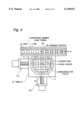
- FIG. 3 is a diagrammatic plan view of a first embodiment of the die-bonding machine in accordance with the present invention.
- FIG. 4 is a diagrammatic side sectional view of the mechanism shown in FIG. 3;
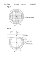
- FIG. 5 diagrammatically illustrate the array of pellets held by a ring holder
- FIG. 6 is a diagrammatic partial plan view of a second embodiment of the die-bonding machine in accordance with the present invention.
- FIG. 3 there is shown a diagrammatic plan view of a first embodiment of the die-bonding machine in accordance with the present invention.
- FIG. 4 is a diagrammatic side sectional view of the mechanism shown in FIG. 3.
- the die-bonding machine includes a rail 2 extending in a horizontal direction in FIG. 3, and a supporting member 1 such as a lead frame having a series of lands 1a (on which a bonding agent such as a solder or a silver (Ag) paste was placed in a preceding step), is placed on the rail 2, and is intermittently fed by a land interval in a left-to-right direction in FIG. 3 (namely, in an X direction) and then slopped by a not-shown feeding mechanism so that the land is placed at a predetermined bonding position BP.
- a supporting member 1 such as a lead frame having a series of lands 1a (on which a bonding agent such as a solder or a silver (Ag) paste was placed in a preceding step)
- a bonding agent such as a solder or a silver (Ag) paste was placed in a preceding step
- a number of pellets 3 obtained by dicing a wafer are adhered on a sheet (not shown) to maintain a geometrical arrangement before the wafer is divided into the pellets, and the sheet is fixed to a wafer ring 5.
- the wafer ring 5 is fitted into and held by a ring holder 16, which is supported by a supporting and displacing mechanism 10, as shown in FIG. 4.
- This supporting and displacing mechanism 10 includes an XY table 11 and a rotating mechanism 12 fixed on the XY table 11 and having a rotating shift 13 supporting the ring holder 16 secured to its top end. Therefore, the ring holder 16 can be rotated about a center axis of the rotating shaft 13 by means of the rotating mechanism 12.
- the XY table 11 is coupled to an X-direction driving mechanism 11A for displacing the ring holder 16 in the X direction in parallel to the feeding direction of the supporting member 1.
- the XY table 11 is also coupled to a Y-direction driving mechanism 11B for displacing the ring holder 16 in a Y direction perpendicular to the X direction.
- the center axis of the rotating shaft 13 is perpendicular to the X direction and the Y direction.
- the supporting and displacing mechanism 10 can freely displace the ring holder 6 in the X direction, in the Y direction perpendicular, and in an angular direction (a ⁇ direction), so that a designated pellet is sequentially placed in a pick-up position PX one by one.
- This pick-up position PX is determined to be as near to the bonding position BP as possible in the Y direction.
- the above construction is similar to the prior art die-bonding machine shown in FIGS. 1 and 2.
- the moving range of the ring holder 16 in the X direction is made smaller than that of the prior art die-bonding machine shown in FIGS. 1 and 2.
- the moving range of a center point C of the ring holder 16 is the same at opposite sides of a reference line S which is a Y axis line passing through the die-bonding position BP on the rail 2.
- a moving line L of the pick-up position PX extending in the X direction is set to be as near to the die-bonding position BP as possible.
- a minimum distance is required between the die-bonding position BP and the pick-up position PX, by considering the size of the pellet to be picked up, a locating space for a sensor for confirming that the pellet is sucked to a vacuum nozzle in the pellet picking-up and carrying process, etc.
- a camera 17 is located directly above the pick-up position PX, and an image of the pellet located on the pick-up position PX, is photographed by the camera 17 and processed by a processing and controlling system 20 to ascertain whether or not a bad mark exists in a target pellet, and whether or not an appearance abnormality such as a crack or a chipping exists in the target pellet, and also to confirm that the target pellet is positioned in place on the pick-up position PX.
- a push-up pin 18 is provided under the ring holder 6, in a substantial alignment with the camera 17 in a vertical line. When the pellet is picked up, the push-up pin 18 is elevated to push up the pellet positioned on the pick-up position PX, so as to peel off the pellet from the adhering sheet. Therefore, the camera 17 and the push-up pin 18 are fixed in the Y direction, but are movable in the X direction to displace the pick-up position PX in accordance with a rule which will be explained hereinafter.
- the camera 17 is coupled to a driving mechanism 21 to be displaced along the moving line L of the pick-up position PX
- the push-up pin 18 is coupled to a driving mechanism 22 to be displaced along the moving line L of the pick-up position PX, in synchronism with the displacement of the camera, and to be moved vertically, namely, in the Z direction, for pushing up the pellet positioned on the pick-up position PX.
- the die-bonding machine also includes a pellet picking-up and carrying mechanism having a vacuum nozzle 14.
- the vacuum nozzle 14 is fixed to a tip end of an arm 23 having a base end coupled to a driving mechanism 24.
- the driving mechanism 24 By this driving mechanism 24, the vacuum nozzle 14 can be displaced in the Z direction (vertical direction) and in the Y direction, shown in a dotted line in FIG. 4 and also in the X direction in FIG. 3.
- the supporting and displacing mechanism 10 and the drive mechanisms 21, 22 and 24 are controlled by the processing and controlling system 20
- Pellet arrangement pitches 1X and 1Y are given in the X direction and in the Y direction in the array of pellets 3, respectively.
- the ring holder 16 is displaced in the X direction and in the Y direction in order to locate any pellet, a pellet to be first picked up, at a reference position (for example, a center point) within a viewing field of the camera 17.
- a reference position for example, a center point
- the camera 17 is not displaced in the Y direction, but when the ring holder 16 is displaced in the X direction, the camera 17 is displaced in a -X direction, so as to approach the target pellet to be picked up.
- the ring holder 16 and the camera 17 are displaced while maintaining such a relation that the X-direction coordinate position PX of the camera 17 and the X-direction coordinates CX of the center point C of the ring holder 16 fulfills the following equation:
- the push-up pin 18 is displaced to the same position in the XY coordinates.
- the position of the first pellet 3 in relation to the ring holder 16 can be known from the displacements of the ring holder 16 and the camera 17.
- the arrangement of the array of pellets can be supposed from the pitches 1X and 1Y.
- the pick-up position PX (the position of the camera 17 and the push-up pin 18) is displaced by "1X/2". Interlocking with this displacement of the pick-up position PX, the ring holder 16 is displaced by "-1X/2". As a result, a pellet "b" is located within the viewing field of the camera 17. However, since the pellet "b” shown in FIG. 5 is not a rectangle (because one corner is chipped), the pellet "b” is not picked up, and the pick-up position PX is further displaced by "-1X/2", and the ring holder 16 is further displaced by "-1X/2” interlocking with this further displacement of the pick-up position PX. However, the pellet adjacent to the pellet "b” in the X direction is also not a rectangle, and therefore, the pellet is not picked up, aid the pick-up position PX is further displaced.
- a row is changed. Namely, the ring holder 16 is displaced by "1Y" in the Y direction while maintaining the X-direction pick-up position PX as it is. In this condition, if no pellet is detected on the pick-up position PX, the pick-up position PX is displaced by "-1X/2" and the ring holder 16 is displaced by "1X/2", interlocking with this further displacement of the pick-up position PX.
- the pellet on the new pick-up position is not a rectangle, the pellet is not picked up, and the pick-up position PX is further displaced by "-1X/2" and the ring holder 16 is further displaced by "1X/2", interlocking with this further displacement of the pick-up position PX, so that a pellet "c" is located within the viewing field of the camera 17.
- the machine since the Y direction distance between the die-bonding position BP and the moving line L of a pick-up position PX is made as short as possible, the time for carrying the pellet in the Y direction is shortened. On the other hand, the X-direction pellet carrying distance is generated, which however becomes one fourth of the diameter of the wafer (the diameter of the array of pellets) at maximum. Therefore, the die-bonding operation is somewhat lowered in comparison with the prior art die-bonding machine shown in FIGS. 1 and 2. Furthermore, the moving range of the ring holder 16 in the Y direction becomes a double of the diameter of the wafer, similarly to the prior art die-bonding machine shown in FIGS. 1 and 2, but the moving range of the ring holder 16 in the X direction becomes one and a half times the diameter of the wafer. Correspondingly, the machine can be reduced in size
- the moving range of the ring holder 16 in the X direction is made smaller than that in the prior art die-bonding machine.
- a second embodiment which will be described hereinafter, is so configured that, by displacing a pick-up position PXY in the X direction and in the Y direction, the moving range of the ring holder 16 is made smaller than that in the prior art die-bonding machine not only in the X direction but also in the Y direction.
- FIG. 6 there is shown a diagrammatic partial plan view of the second embodiment of the die-bonding machine in accordance with the present invention.
- This second embodiment is similar to the first embodiment in that the moving range of a center point C of a ring holder 26 is the same at opposite sides of a reference line S which is a Y-axis line passing through a die-bonding position BP on the rail 2.
- the second embodiment has the moving range of the same magnitude at opposite sides of a reference line R extending in the X direction.
- This reference line R is determined in such a manner that when an intersection of the reference line S and the reference line R is positioned on a center point of the ring holder 26, a 1/2-radius position of the wafer (the array of pellets) held by the ring holder 26 is as near to the die-bonding position BP as possible on the reference line S and is at a position which slightly apart from a point PYM which can become a pick-up position, toward the intersection of the reference line S and the reference line R.
- the second embodiment can be realized by slightly modifying the die-bonding machine shown in FIGS. 3 and 4, and by controlling the machine in a different manner.
- the pick-up position PXY is movable both in the X direction and in the Y direction, and therefore, the camera 17 and the push-up pin 18 are also movable both in the X direction and in the Y direction.
- the vacuum nozzle 14 provided at a tip end of the pellet picking-up and carrying mechanism can be displaced in the X, Y and Z directions, so that the pellet is picked up at the pick-up position PXY, and carried to the die-bonding position BP, and then, placed on the land of the supporting member in the pick-up position PXY, for a die-bonding.
- the ring holder 26 is rotated to make the array of pellets 3 in parallel to the X direction and the Y direction.
- pellet arrangement pitches 1X and 1Y are provided in the X direction and in the Y direction in the array of pellets 3, respectively.
- the ring holder 26 is displaced in the X direction and in the Y direction in order to locate any pellet, a pellet to be first picked up, at a reference position (for example, a center point) within a viewing field of the camera 17. The operation until this point is similar to that of the first embodiment.
- the push-up pin 18 is displaced to the same position in the XY coordinates.
- the position of the first pellet 3 in relation to the ring holder 26 can be known from the displacements of the ring holder 26 and the camera 17.
- the arrangement of the array of pellets can be supposed from the pitches 1X and 1Y.
- the pick-up position PXY (the position of the camera 17 and the push-up pin 18) is displaced by "1X/2" in the X coordinates, without changing the pick-up position PXY in the Y coordinates.
- the ring holder 26 is displaced by "-1X/2" in the X coordinates, without changing the center position CXY of the ring holder 26 in the Y coordinates.
- a pellet "b" is located within the viewing field of the camera 17. However, since the pellet "b" shown in FIG.
- the pellet on the new pick-up position is not a rectangle, the pellet is not picked up, and the pick-up position PXY is further displaced by "-1X/2" without being displaced in the Y direction, and the ring holder 26 is further displaced by "1X/2" without being displaced in the Y direction, interlocking with the displacement of the pick-up position PXY, so that a pellet "c" is located within the viewing field of the camera 17.
- the machine can be reduced in size
- the die-bonding machine in accordance with the present invention can make the moving range of the pellet supporting and displacing mechanism as small as possible without seriously lowering the speed of the die-bonding operation, the size of the die-bonding machine can be reduced.
- the control software can be simplified.
Applications Claiming Priority (2)
| Application Number | Priority Date | Filing Date | Title |
|---|---|---|---|
| JP10-176014 | 1998-06-23 | ||
| JP17601498A JP3971848B2 (ja) | 1998-06-23 | 1998-06-23 | ダイボンダ |
Publications (1)
| Publication Number | Publication Date |
|---|---|
| US6149047A true US6149047A (en) | 2000-11-21 |
Family
ID=16006222
Family Applications (1)
| Application Number | Title | Priority Date | Filing Date |
|---|---|---|---|
| US09/339,029 Expired - Fee Related US6149047A (en) | 1998-06-23 | 1999-06-23 | Die-bonding machine |
Country Status (4)
| Country | Link |
|---|---|
| US (1) | US6149047A (ja) |
| JP (1) | JP3971848B2 (ja) |
| KR (1) | KR100303960B1 (ja) |
| TW (1) | TW419757B (ja) |
Cited By (17)
| Publication number | Priority date | Publication date | Assignee | Title |
|---|---|---|---|---|
| US20010051394A1 (en) * | 1998-09-30 | 2001-12-13 | Sang-Geun Kim | Die bonding equipment |
| US20020000294A1 (en) * | 2000-07-03 | 2002-01-03 | Esec Trading Sa | Method and apparatus for mounting semiconductor chips onto a flexible substrate |
| EP1209723A1 (en) * | 2000-11-27 | 2002-05-29 | ASM Assembly Automation Limited | A wafer table for die bonding apparatus |
| WO2003015489A2 (en) * | 2001-08-08 | 2003-02-20 | Matsushita Electric Industrial Co., Ltd. | Apparatus and method for mounting electronic parts |
| US6575351B1 (en) * | 1999-06-18 | 2003-06-10 | Shibuya Kogyo Co., Ltd. | Work/head positioning apparatus for ball mount apparatus |
| US20040254669A1 (en) * | 2003-05-28 | 2004-12-16 | Badar Omar Mohd | Automatic recognition of locator die in partial wafermap process |
| EP1581040A2 (en) * | 2004-03-26 | 2005-09-28 | Matsushita Electric Industrial Co., Ltd. | Electronic component mounting apparatus and electronic component mounting method |
| US20050284578A1 (en) * | 2004-06-24 | 2005-12-29 | Sharp Kabushiki Kaisha | Bonding apparatus, bonding method, and method for manufacturing semiconductor device |
| EP1612843A1 (de) * | 2004-07-02 | 2006-01-04 | Unaxis International Trading Ltd | Verfahren und Einrichtung fuer die Montage von Halbleiterchips |
| KR100559725B1 (ko) * | 2000-11-27 | 2006-03-10 | 에이에스엠 어쌤블리 오토메이션 리미티드 | 다이본딩장치 |
| CN101364530B (zh) * | 2007-08-10 | 2011-12-28 | Juki株式会社 | 电子部件安装方法及装置 |
| CN103159167A (zh) * | 2013-03-22 | 2013-06-19 | 常熟艾科瑞思封装自动化设备有限公司 | 传感器封装设备 |
| CN103177976A (zh) * | 2013-03-22 | 2013-06-26 | 常熟艾科瑞思封装自动化设备有限公司 | 二极管封装方法 |
| CN103946966A (zh) * | 2011-11-18 | 2014-07-23 | 富士机械制造株式会社 | 晶圆关联数据管理方法及晶圆关联数据生成装置 |
| US20150170944A1 (en) * | 2012-07-20 | 2015-06-18 | Rokko Systems Pte Ltd. | Method and apparatus for the engagement of ic units |
| EP2938176A4 (en) * | 2012-12-20 | 2015-12-02 | Fuji Machine Mfg | DEVICE FOR SUPPLYING CHIPS |
| CN110024098A (zh) * | 2016-12-06 | 2019-07-16 | 株式会社富士 | 裸片元件供给装置 |
Families Citing this family (5)
| Publication number | Priority date | Publication date | Assignee | Title |
|---|---|---|---|---|
| JP4530504B2 (ja) * | 1999-08-27 | 2010-08-25 | パナソニック株式会社 | 整列部品の取扱装置 |
| JP2002270622A (ja) * | 2001-03-09 | 2002-09-20 | Ueno Seiki Kk | 電子部品自動ハンドリング装置用電子部品保持機構及び電子部品保持方法 |
| DE10159976A1 (de) * | 2001-12-06 | 2003-08-14 | Michael Geringer | Vorrichtung zum Handhaben von Bauelementen mit kleinen Abmessungen |
| JP4409136B2 (ja) * | 2001-12-18 | 2010-02-03 | パナソニック株式会社 | 電子部品搭載装置および電子部品搭載方法 |
| JP4909249B2 (ja) * | 2007-12-03 | 2012-04-04 | アクテス株式会社 | 移載装置 |
Citations (2)
| Publication number | Priority date | Publication date | Assignee | Title |
|---|---|---|---|---|
| JPH01152634A (ja) * | 1987-12-09 | 1989-06-15 | Rohm Co Ltd | 半導体ペレットの組立装置 |
| JPH04111330A (ja) * | 1990-08-31 | 1992-04-13 | Toshiba Corp | 半導体製造装置 |
-
1998
- 1998-06-23 JP JP17601498A patent/JP3971848B2/ja not_active Expired - Fee Related
-
1999
- 1999-06-22 TW TW088110443A patent/TW419757B/zh not_active IP Right Cessation
- 1999-06-23 KR KR1019990023652A patent/KR100303960B1/ko not_active IP Right Cessation
- 1999-06-23 US US09/339,029 patent/US6149047A/en not_active Expired - Fee Related
Patent Citations (2)
| Publication number | Priority date | Publication date | Assignee | Title |
|---|---|---|---|---|
| JPH01152634A (ja) * | 1987-12-09 | 1989-06-15 | Rohm Co Ltd | 半導体ペレットの組立装置 |
| JPH04111330A (ja) * | 1990-08-31 | 1992-04-13 | Toshiba Corp | 半導体製造装置 |
Cited By (40)
| Publication number | Priority date | Publication date | Assignee | Title |
|---|---|---|---|---|
| US20010051394A1 (en) * | 1998-09-30 | 2001-12-13 | Sang-Geun Kim | Die bonding equipment |
| US6820792B2 (en) * | 1998-09-30 | 2004-11-23 | Samsung Electronics Co., Ltd. | Die bonding equipment |
| KR100598198B1 (ko) * | 1999-06-18 | 2006-07-07 | 시부야 코교 가부시키가이샤 | 피가공물과 헤드의 위치결정장치 및 위치결정방법 |
| US6575351B1 (en) * | 1999-06-18 | 2003-06-10 | Shibuya Kogyo Co., Ltd. | Work/head positioning apparatus for ball mount apparatus |
| US6821375B2 (en) * | 2000-07-03 | 2004-11-23 | Esec Trading Sa | Method and apparatus for mounting semiconductor chips onto a flexible substrate |
| US20020000294A1 (en) * | 2000-07-03 | 2002-01-03 | Esec Trading Sa | Method and apparatus for mounting semiconductor chips onto a flexible substrate |
| EP1209723A1 (en) * | 2000-11-27 | 2002-05-29 | ASM Assembly Automation Limited | A wafer table for die bonding apparatus |
| US6543513B1 (en) | 2000-11-27 | 2003-04-08 | Asm Assembly Automation Ltd. | Wafer table for die bonding apparatus |
| KR100559725B1 (ko) * | 2000-11-27 | 2006-03-10 | 에이에스엠 어쌤블리 오토메이션 리미티드 | 다이본딩장치 |
| US6792676B2 (en) | 2001-08-08 | 2004-09-21 | Matsushita Electric Industrial Co., Ltd. | Apparatus and method for mounting electronic parts |
| US20040148769A1 (en) * | 2001-08-08 | 2004-08-05 | Matsushita Electric Industrial Co., Ltd. | Apparatus and method for mounting electronic parts |
| WO2003015489A3 (en) * | 2001-08-08 | 2003-10-30 | Matsushita Electric Ind Co Ltd | Apparatus and method for mounting electronic parts |
| US7137195B2 (en) | 2001-08-08 | 2006-11-21 | Matsushita Electric Industrial Co., Ltd. | Method for mounting electronic parts onto a board |
| WO2003015489A2 (en) * | 2001-08-08 | 2003-02-20 | Matsushita Electric Industrial Co., Ltd. | Apparatus and method for mounting electronic parts |
| US20040254669A1 (en) * | 2003-05-28 | 2004-12-16 | Badar Omar Mohd | Automatic recognition of locator die in partial wafermap process |
| US6937916B2 (en) * | 2003-05-28 | 2005-08-30 | Texas Instruments Incorporated | Automatic recognition of locator die in partial wafermap process |
| EP1581040A3 (en) * | 2004-03-26 | 2007-10-24 | Matsushita Electric Industrial Co., Ltd. | Electronic component mounting apparatus and electronic component mounting method |
| EP1581040A2 (en) * | 2004-03-26 | 2005-09-28 | Matsushita Electric Industrial Co., Ltd. | Electronic component mounting apparatus and electronic component mounting method |
| KR101108136B1 (ko) | 2004-03-26 | 2012-01-31 | 파나소닉 주식회사 | 전자부품 탑재장치 및 전자부품 탑재방법 |
| US20050284578A1 (en) * | 2004-06-24 | 2005-12-29 | Sharp Kabushiki Kaisha | Bonding apparatus, bonding method, and method for manufacturing semiconductor device |
| DE102005029136B4 (de) * | 2004-07-02 | 2008-03-27 | Unaxis International Trading Ltd. | Verfahren und Einrichtung für die Montage von Halbleiterchips |
| US7415759B2 (en) | 2004-07-02 | 2008-08-26 | Unaxis International Trading Ltd. | Method and apparatus for mounting semiconductor chips |
| US20080301931A1 (en) * | 2004-07-02 | 2008-12-11 | Unaxis International Trading Ltd. | Method And Apparatus For Mounting Semiconductor Chips |
| EP1612843A1 (de) * | 2004-07-02 | 2006-01-04 | Unaxis International Trading Ltd | Verfahren und Einrichtung fuer die Montage von Halbleiterchips |
| US20060000082A1 (en) * | 2004-07-02 | 2006-01-05 | Unaxis International Trading Ltd | Method and apparatus for mounting semiconductor chips |
| CN101364530B (zh) * | 2007-08-10 | 2011-12-28 | Juki株式会社 | 电子部件安装方法及装置 |
| US9378993B2 (en) | 2011-11-18 | 2016-06-28 | Fuji Machine Mfg. Co., Ltd. | Wafer-related data management method and wafer-related data creation device |
| CN103946966A (zh) * | 2011-11-18 | 2014-07-23 | 富士机械制造株式会社 | 晶圆关联数据管理方法及晶圆关联数据生成装置 |
| EP2782125A1 (en) * | 2011-11-18 | 2014-09-24 | Fuji Machine Mfg. Co., Ltd. | Wafer-related data management method and wafer-related data creation device |
| EP2782125A4 (en) * | 2011-11-18 | 2015-04-29 | Fuji Machine Mfg | METHOD OF MANAGING DATA ASSOCIATED WITH A WAFER AND DEVICE FOR CREATING DATA ASSOCIATED WITH A WAFER |
| CN103946966B (zh) * | 2011-11-18 | 2016-06-08 | 富士机械制造株式会社 | 晶圆关联数据管理方法及晶圆关联数据生成装置 |
| US20150170944A1 (en) * | 2012-07-20 | 2015-06-18 | Rokko Systems Pte Ltd. | Method and apparatus for the engagement of ic units |
| EP2938176A4 (en) * | 2012-12-20 | 2015-12-02 | Fuji Machine Mfg | DEVICE FOR SUPPLYING CHIPS |
| CN103177976A (zh) * | 2013-03-22 | 2013-06-26 | 常熟艾科瑞思封装自动化设备有限公司 | 二极管封装方法 |
| CN103159167B (zh) * | 2013-03-22 | 2015-09-30 | 江苏艾科瑞思封装自动化设备有限公司 | 传感器封装设备 |
| CN103177976B (zh) * | 2013-03-22 | 2015-07-01 | 江苏艾科瑞思封装自动化设备有限公司 | 二极管封装方法 |
| CN103159167A (zh) * | 2013-03-22 | 2013-06-19 | 常熟艾科瑞思封装自动化设备有限公司 | 传感器封装设备 |
| CN110024098A (zh) * | 2016-12-06 | 2019-07-16 | 株式会社富士 | 裸片元件供给装置 |
| EP3553813A4 (en) * | 2016-12-06 | 2020-01-01 | Fuji Corporation | DEVICE FOR PROVIDING MATRIX ELEMENTS |
| US10879096B2 (en) | 2016-12-06 | 2020-12-29 | Fuji Corporation | Die component supply device |
Also Published As
| Publication number | Publication date |
|---|---|
| TW419757B (en) | 2001-01-21 |
| KR100303960B1 (ko) | 2001-11-01 |
| JP2000012568A (ja) | 2000-01-14 |
| KR20000006373A (ko) | 2000-01-25 |
| JP3971848B2 (ja) | 2007-09-05 |
Similar Documents
| Publication | Publication Date | Title |
|---|---|---|
| US6149047A (en) | Die-bonding machine | |
| US7727800B2 (en) | High precision die bonding apparatus | |
| KR102196105B1 (ko) | 전자 부품의 실장 장치와 실장 방법, 및 패키지 부품의 제조 방법 | |
| JP2003526935A (ja) | 改善された画像システムを備えた選出配置装置 | |
| KR20170110651A (ko) | 절단 장치 및 절단 방법 | |
| US20060000082A1 (en) | Method and apparatus for mounting semiconductor chips | |
| JP6522797B2 (ja) | ダイピックアップ装置 | |
| KR20160110110A (ko) | 본딩 장치 및 본딩 방법 | |
| KR100881894B1 (ko) | 전자 부품 탑재 장치 및 전자 부품 탑재 방법 | |
| KR102132094B1 (ko) | 전자 부품 실장 장치 및 전자 부품 실장 방법 | |
| EP2059112B1 (en) | Electronic component taking out apparatus, surface mounting apparatus and method for taking out electronic component | |
| JP2000150970A (ja) | 発光素子のボンディング方法および装置 | |
| JP2000114281A (ja) | ダイボンディング方法およびダイボンディング設備 | |
| JPH11102936A (ja) | 部品供給装置及び方法 | |
| US20020162217A1 (en) | Apparatus for placing a semiconductor chip as a flipchip on a substrate | |
| JP2003318599A (ja) | 部品実装方法及び部品実装装置 | |
| WO2019097675A1 (ja) | 部品実装機、部品検査方法、部品検査プログラム、記録媒体 | |
| US20110182701A1 (en) | Method and apparatus for transferring die from a wafer | |
| US6315185B2 (en) | Ball mount apparatus | |
| JPH06268050A (ja) | ダイスボンディング装置 | |
| JP4761672B2 (ja) | ボンディング方法及びボンディング装置 | |
| JP3272312B2 (ja) | 位置認識手段の移動装置 | |
| JPH09232407A (ja) | ワーク搬送装置およびそれを用いた半導体製造装置 | |
| US8633089B2 (en) | Die bonding method utilizing rotary wafer table | |
| JPH0213934B2 (ja) |
Legal Events
| Date | Code | Title | Description |
|---|---|---|---|
| AS | Assignment |
Owner name: NEC CORPORATION, JAPAN Free format text: ASSIGNMENT OF ASSIGNORS INTEREST;ASSIGNOR:ODA, NORIO;REEL/FRAME:010142/0652 Effective date: 19990623 |
|
| AS | Assignment |
Owner name: NEC MACHINERY CORPORATION, JAPAN Free format text: ASSIGNMENT OF ASSIGNORS INTEREST;ASSIGNOR:NEC CORPORATION;REEL/FRAME:011516/0902 Effective date: 20001226 |
|
| REMI | Maintenance fee reminder mailed | ||
| LAPS | Lapse for failure to pay maintenance fees | ||
| STCH | Information on status: patent discontinuation |
Free format text: PATENT EXPIRED DUE TO NONPAYMENT OF MAINTENANCE FEES UNDER 37 CFR 1.362 |
|
| FP | Lapsed due to failure to pay maintenance fee |
Effective date: 20041121 |