US5609967A - Decorative plate - Google Patents
Decorative plate Download PDFInfo
- Publication number
- US5609967A US5609967A US08/369,404 US36940495A US5609967A US 5609967 A US5609967 A US 5609967A US 36940495 A US36940495 A US 36940495A US 5609967 A US5609967 A US 5609967A
- Authority
- US
- United States
- Prior art keywords
- decorative plate
- lines
- layer
- plating
- substrate
- Prior art date
- Legal status (The legal status is an assumption and is not a legal conclusion. Google has not performed a legal analysis and makes no representation as to the accuracy of the status listed.)
- Expired - Lifetime
Links
Images


Classifications
-
- B—PERFORMING OPERATIONS; TRANSPORTING
- B44—DECORATIVE ARTS
- B44C—PRODUCING DECORATIVE EFFECTS; MOSAICS; TARSIA WORK; PAPERHANGING
- B44C1/00—Processes, not specifically provided for elsewhere, for producing decorative surface effects
- B44C1/22—Removing surface-material, e.g. by engraving, by etching
-
- B—PERFORMING OPERATIONS; TRANSPORTING
- B41—PRINTING; LINING MACHINES; TYPEWRITERS; STAMPS
- B41M—PRINTING, DUPLICATING, MARKING, OR COPYING PROCESSES; COLOUR PRINTING
- B41M1/00—Inking and printing with a printer's forme
- B41M1/12—Stencil printing; Silk-screen printing
-
- G—PHYSICS
- G03—PHOTOGRAPHY; CINEMATOGRAPHY; ANALOGOUS TECHNIQUES USING WAVES OTHER THAN OPTICAL WAVES; ELECTROGRAPHY; HOLOGRAPHY
- G03F—PHOTOMECHANICAL PRODUCTION OF TEXTURED OR PATTERNED SURFACES, e.g. FOR PRINTING, FOR PROCESSING OF SEMICONDUCTOR DEVICES; MATERIALS THEREFOR; ORIGINALS THEREFOR; APPARATUS SPECIALLY ADAPTED THEREFOR
- G03F7/00—Photomechanical, e.g. photolithographic, production of textured or patterned surfaces, e.g. printing surfaces; Materials therefor, e.g. comprising photoresists; Apparatus specially adapted therefor
- G03F7/12—Production of screen printing forms or similar printing forms, e.g. stencils
-
- Y—GENERAL TAGGING OF NEW TECHNOLOGICAL DEVELOPMENTS; GENERAL TAGGING OF CROSS-SECTIONAL TECHNOLOGIES SPANNING OVER SEVERAL SECTIONS OF THE IPC; TECHNICAL SUBJECTS COVERED BY FORMER USPC CROSS-REFERENCE ART COLLECTIONS [XRACs] AND DIGESTS
- Y10—TECHNICAL SUBJECTS COVERED BY FORMER USPC
- Y10T—TECHNICAL SUBJECTS COVERED BY FORMER US CLASSIFICATION
- Y10T428/00—Stock material or miscellaneous articles
- Y10T428/12—All metal or with adjacent metals
- Y10T428/12389—All metal or with adjacent metals having variation in thickness
- Y10T428/12396—Discontinuous surface component
-
- Y—GENERAL TAGGING OF NEW TECHNOLOGICAL DEVELOPMENTS; GENERAL TAGGING OF CROSS-SECTIONAL TECHNOLOGIES SPANNING OVER SEVERAL SECTIONS OF THE IPC; TECHNICAL SUBJECTS COVERED BY FORMER USPC CROSS-REFERENCE ART COLLECTIONS [XRACs] AND DIGESTS
- Y10—TECHNICAL SUBJECTS COVERED BY FORMER USPC
- Y10T—TECHNICAL SUBJECTS COVERED BY FORMER US CLASSIFICATION
- Y10T428/00—Stock material or miscellaneous articles
- Y10T428/12—All metal or with adjacent metals
- Y10T428/12486—Laterally noncoextensive components [e.g., embedded, etc.]
Definitions
- This invention relates to a decorative plate prepared by using a negative or a positive photographic film and a process for preparing the same, and particularly to a decorative plate in which a pattern is formed on a metal plate by plating and a process for preparing the same.
- the appearance of an image or a pattern formed on a metallic decorative plate or card is particularly good when the plate or card is formed having a substrate with a stainless steel surface.
- the quality of the appearance is due in part to the metallic color of a plating layer formed on the stainless steel surface, and in part to the degree which the plating layer adheres to the stainless steel. Images or patterns formed on these types of decorative plates are used for name plates, trading cards or the like.
- This kind of a decorative plate and a process by which the plate is prepared were previously proposed by the present inventors (Japanese Unexamined Patent Publication No. 1-306592).
- the steps involved in the preparation process include forming an ink layer as a masking layer on a stainless steel surface of the substrate, removing an oxidized film on that portion of the substrate's surface not covered by an ink layer and carrying out plating treatment so that a pattern is formed on a portion of the substrate's surface where the coating film has been removed.
- a decorative plate having a plating layer portion on a metal substrate comprising:
- a plurality of lines representing a degree of a shade of a pattern said lines being formed on one selected from a group consisting of the layer portion and portions other than the layer portion in the plate.
- FIG. 1 is a perspective view illustrating a decorative plate of a first embodiment of the present invention
- FIG. 2 is a perspective view illustrating a screen having predetermined meshes
- FIG. 3 is a perspective view illustrating a negative film
- FIG. 4 is a partial enlarged view illustrating the negative film
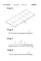
- FIG. 5 is a perspective view illustrating a stainless steel plate
- FIG. 6 is a sectional view of the decorative plate illustrating the formation of a resin layer on a screen
- FIG. 7 is a sectional view of the decorative plate illustrating the process of irradiating light through a negative film placed above the screen;
- FIG. 8 is a sectional view of the decorative plate illustrating a pattern of cured resin on the screen after the removal of uncured resin
- FIG. 9 is a sectional view of the decorative plate illustrating the formation of the screen absent the uncured resin removed on a stainless steel plate
- FIG. 10 is a sectional view of the decorative plate illustrating the formation of an ink layer on the stainless steel plate by printing
- FIG. 11 is a sectional view of the decorative plate illustrating the formation of a primary plating layer on the stainless steel plate
- FIG. 12 is a sectional view of the decorative plate illustrating the formation of a copper plating layer on the primary plating layer
- FIG. 13 is a sectional view of the decorative plate illustrating the formation of a nickel plating layer on the copper plating layer;
- FIG. 14 is a sectional view of the decorative plate illustrating the formation of a gold plating layer on the nickel plating layer;
- FIG. 15 is a sectional view of the decorative plate illustrating the formation of the ink layer is removed from the surface of the substrate;
- FIG. 16 is an enlarged sectional view of the decorative plate illustrating various patterns of light reflection off of the plating layer
- FIG. 17 is a sectional view of the decorative plate illustrating the formation of a light-sensitive resin layer on a color stainless steel plate of a second embodiment
- FIG. 18 is a sectional view of the decorative plate illustrating the process of irradiating UV rays through a negative film to the plate of FIG. 17;
- FIG. 19 is a sectional view of the decorative plate illustrating the formation of a cured resin layer on the plate of FIG. 18;
- FIG. 20 is a sectional view of the decorative plate illustrating the formation of concave portions produced by etching the surface of the stainless steel plate of FIG. 19;
- FIG. 21 is a sectional view of the decorative plate illustrating the formation of a gold plating layer on concave portions of the present invention as shown in FIG. 20;
- FIG. 22 is a sectional view showing the plate of FIG. 21 with the cured resin layer removed.
- FIGS. 1 through 16 A first embodiment of the present invention is described below with reference to FIGS. 1 through 16.
- a decorative plate bearing an image or decorative pattern on a substrate is described along with the process for making the same using photographic film or the like.
- the thicknesses of the respective layers such as plating layers are enlarged to more clearly illustrate the features of the invention.
- a decorative plate 1 is a metal card in which the likeness of a person or other object is formed using a gold plating layer 3 on a substrate 2 made of stainless steel.
- the size of the substrate 2 can be, for example, a length of about 9 cm, a width of about 7 cm and a thickness of about 1.5 mm.
- the plating is formed on the substrate 2 using the photograph of the person.
- the gold plating layer 3 on the decorative plate 1 is formed on a portion other than a large number of lines 4 made at predetermined intervals.
- the lines 4 include oblique lines 40 portraying the likeness of the person and horizontal lines 41 that serve as a background to the oblique lines 40.
- photographic negative film 7 containing the image or likeness of a person as shown in FIG. 3 and a substrate 20 as shown in FIG. 5 are prepared.
- the substrate 20 contains multiple pieces, here the substrate 20 is shown having twelve decorative plates.
- the image on the negative film 7 comprises a large number of lines 5.
- the portraits comprise lines 50 made in the oblique direction, and the background comprises lines 51 made in the horizontal direction.
- the shadow and gradation of the images are expressed by varying the thicknesses of the lines 5.
- the negative film 7 described above is prepared as shown in FIGS. 3 and 4.
- a large number of the lines 5 of the negative film 7 are made at predetermined intervals.
- the density of the lines 5 is preferably 50 to 80 lines/inch for the following reasons.
- the plating width i.e., the distance separating the lines increases to a point making it appear that the plating layers are continuously formed across the substrate 20. This makes it difficult to discern any gradations that may be formed in the pattern.
- the line density is greater than the above range, the lines 5 adjacent to each other, appear to contact each other making it difficult to form a pattern.
- a mesh screen 8 shown in FIG. 2 is made of polyester type fiber, and is coated with a light-sensitive resin solution.
- the mesh size of the screen 8 is 200 to 300 mesh.
- a resin layer 9 having a thickness of 10 to 20 ⁇ m is formed.
- the resin layer 9 is formed thin over the entire surface of the screen 8 ensuring the precise formation of the complicated pattern.
- the resin layer 9 is formed thick because the patterns can be easily formed.
- a photocurable acrylic resin or the like can be used as the light-sensitive resin.
- the negative film 7 is placed above the screen 8 on which the above resin layer 9 is formed, and UV rays are irradiated from the upper direction. Irradiation of UV rays cures the light-sensitive resin under the transparent portions of the film 7, i.e., at portions other than at the lines 5 and thick line portions 6. This forms a cured resin layer 10.
- uncured resin portions other than the cured resin layer 10 on the screen 8 are removed from the screen 8 by flowing water on the screen 8. Then, only the cured resin layer 10 remains on the screen 8. Portions of the screen 8, not covered by the cured resin layer 10, comprise lines made at predetermined intervals corresponding to the above negative film 7. For this reason, the screen 8 is often called a line screen.
- the screen 8 on which the cured resin layer 10 is formed is mounted on the substrate 20 which is subjected to mirror polishing.
- Silk screen printing is then performed on the screen 8 to form an ink layer 12 on the substrate 20 as a masking layer corresponding to the portions other than the cured resin layer 10.
- the ink used in this process may be, for example, a type produced under the trade name by YOSHIKAWA CHEMICAL CO. [containing a resin (a hydrocarbon derivative), a solvent (aromatic hydrocarbon) and a pigment (talc) as main components].
- a resin a hydrocarbon derivative
- a solvent aromatic hydrocarbon
- talc a pigment
- Another example of a suitable ink is produced under the trade name M85K by TAIYO INK MFG. CO., LTD.
- Other acceptable inks may take the form of a plating resist or an etching resist used when a printed substrate is prepared.
- the masking step comprises the steps of coating the light-sensitive resin, curing the resin, removing the uncured resin and forming the ink layer as described above.
- anodic electrolysis is performed to reduce an oxidized layer coating on the surface of the substrate 20.
- the oxygen in the atmosphere oxidizes the surface of the stainless steel.
- the steel thus in a passive state, oxidizes simply by being exposed to the atmosphere.
- the electrolysis is performed by using a 50% aqueous sulfuric acid solution.
- the anodic electrolysis is carried out by dipping the substrate 20 as an anode in an electrolyte and applying an electric current to the electrolyte at a current density of 1 to 6 A/dm 2 for 10 to 60 seconds. This effectively removes the oxidized coating from those portions of the substrate 20 not covered by the ink layer 12.
- the substrate 20 next undergoes electrolytic plating at portions other than where the ink layer 12 is formed on the substrate 20.
- This process forms plating layer 13.
- the ink layer 12 effectively acts as an insulator, so that the plating layer 13 is not formed on the surface of the ink layer 12.
- the plating layer 13 is a layer obtained by laminating plural plating layers which will be described later.
- the plating layer 13 is formed according to the following steps (i) to (iv).
- Nickel plating is effected by dipping the substrate 20 in an electrolyte comprising 100 g/l of hydrochloric acid (HCl) and 250 g/l of nickel chloride (NiCl 2 ).
- the nickel plating is carried out by applying an electric current to the electrolyte at ordinary temperature at a current density of 3 to 5 A/dm 2 for 30 seconds to 2 minutes.
- the primary plating treatment forms a primary plating layer 14 on portions other than where the ink layer 12 has been applied to the substrate 20.
- the thickness of the primary plating layer 14 is about 0.1 to 0.2 ⁇ m.
- Copper plating is performed by dipping the primary plated substrate 20 in an electrolyte comprising 170 g/l of copper sulfate (CuSO 4 ), 50 g/l of sulfuric acid and 45 ml of a gloss agent (Such as in the product produced under the trade name cupracid 210 by OKUNO CHEMICAL IND. CO., LTD). As shown in FIG. 12, a copper plating layer 15 is formed on the primary plating layer 14.
- the gloss agent is added for the purposes of obtaining gloss of the surface of the resulting plating layer and also for smoothing the surface of the plating layer, i.e., improving the leveling property of the plating layer.
- the copper plating is carried out by applying an electric current to the electrolyte at ordinary temperature at a current density of 2 to 5 A/dm 2 for 60 to 120 minutes.
- the relatively thick copper plating layer 15, thus firmed is about 40 to 80 ⁇ m.
- Nickel plating is performed by dipping the copper plated substrate 20 in an electrolyte comprising 45 g/l of nickel chloride (NiCl 2 ) and small amounts of nickel sulfate (NiSO 4 ), boric acid (H 3 BO 3 ) and a gloss agent (such as in the product produced under the trade name Topreona NL-1 by OKUNO CHEMICAL IND. CO., LTD).
- the nickel plating is carried out by applying an electric current to the electrolyte at ordinary temperature at a current density of 3 to 5 A/dm for 30 seconds to 2 minutes.
- a nickel plating layer 16 is formed on the copper plating layer 15.
- the thickness of the nickel plating layer 16 is about 2 to 3 ⁇ m.
- the nickel plated substrate 20 is subject to a gold plating electrolysis process using an aqueous solution comprising 3 g/l of a product produced under the trade name Auro Glo JR 75 by Meltex Co.
- Auro Glo JR 75 is essentially a potassium cyanoaurate (K(Au(CN) 4 )) product.
- a 750 ml/l of a vat solution containing cobalt and 10 ml/l of a replenishing solution also containing cobalt is used as an electrolyte.
- Gold plating is carried out by applying an electric current to the electrolyte at 40° to 50° C. at a current density of 0.2 to 0.5 A/dm 2 for 1.5 to 2.5 minutes.
- a gold plating layer 17 is formed on the nickel plating layer 16.
- the thickness of the gold plating layer 17 formed by the plating is about 0.1 ⁇ m.
- the substrate 20 after completion of the plating treatments is dipped in a hydrocarbon based organic solvent.
- a hydrocarbon based organic solvent By applying ultrasonic vibration to the organic solvent, the ink layer 12 on the surface of the substrate 20 is removed by dissolution. Finally, the surface of the substrate 20 is washed with water. At this time, if the substrate 20 is a color substrate, color tones are formed at the portions from which the ink layer 12 is removed.
- the substrate 20 is punched by a pressing machine and divided into plural substrates (12 substrates in this embodiment) to produce the desired decorative plate 1.
- This decorative plate 1 can be used as a metal card, such as a so-called trading card.
- the shadow of the pattern portion can be expressed clearly by a difference in thickness of the lines. Further, the amount of reflected light varies depending on the angle at which the decorative plate is seen, so that the card's color tone also varies. For example, facial expression of the portrait of the pattern can be various displayed. Therefore, the pattern of the decorative plate 1 looks like a photograph and has excellent decorative property, due to the following reason.
- the pattern and background of the negative film 7 are based on large numbers of the lines 5 set apart from each other at predetermined intervals, the gold plating layer 3, expressing the pattern and background captured on the negative film 7 is based on the lines 4, and reflection of light occurs at the respective lines 4.
- the multilayered plating layer 13 includes a corner portion 18, at the top of the plating layer 13, which is formed in a circular arc shape. This construction causes light incident at the corner portion 18 to be reflected at various angles. Pattern distinctiveness is enhanced by the contrast between the portion corresponding to the portrait of the pattern is formed of the oblique lines 40 and the background portion is formed of the horizontal lines 41.
- the plating layer 13 is formed only after removal of the oxidized coating on the surface of substrate 20 is removed. This ensures a high degree of adhesiveness of the plating layer 13 to the substrate 20. In the event that flexural stress deforms the decorative pattern portion of the decorative plate 1 or that an impact force is applied to the decorative plate 1 by dropping it, or that the decorative plate 1 is exposed to corrosion, the plating layer 13 at the pattern portion will not peel off of the substrate 20. Thus, the decorative plate 1 has excellent durability.
- the substrate 20 is made of stainless steel and its surface has gloss of a silver color or a desired color and weighty appearance, whereby it is suitable as a decorative plate.
- a second embodiment of the present invention will now be described with reference to FIGS. 17 to 22.
- a light-sensitive resin is directly coated on a colored stainless steel plate.
- gold plating is performed. The following steps describe the process of forming a decorative plate according to the second embodiment.
- a stainless steel plate having a predetermined color As a metal plate, a stainless steel plate having a predetermined color is used. As shown in FIG. 17, a resin layer 9 is formed on the surface of the color stainless steel plate 2 by silk screen printing of an acrylic light-sensitive resin peeled using an alkali product produced under the trade name Photomal ET by Okuno Seiyaku Kogyo Co. The resin layer 9 is uniformly coated on the surface of the color stainless steel plate 2. In this case, the light-sensitive resin may be also coated by a roll coater or the like.
- a negative film 7 on which the same images as in the first embodiment are formed is prepared. Portions of the negative film 7 corresponding to the gold plated portion of the substrate 20, are developed black in order to block the transmission of light through the film at those portions.
- the negative film 7 is placed above the color stainless steel plate 2 formed with the resin layer 9, as shown in FIG. 18.
- UV rays are irradiated through the negative film 7 by a UV ray irradiator to carry out printing of the light-sensitive resin.
- the UV irradiation can take place at a distance of 30 cm from the color stainless steel plate 2 for 1 minute by a mercury lamp with an output of 3 KW.
- an uncured light-sensitive resin on the color stainless steel plate 2 is removed by washing with a 1 to 3% aqueous sodium carbonate solution.
- a cured resin layer 10 as a masking layer is formed on the color stainless steel plate 2 in this step.
- surface potions of the color stainless steel plate 2 not having the cured resin layer 10 are etched with a 50% aqueous sulfuric acid solution.
- the anode is made of the color stainless steel plate 2.
- Color portions of the color stainless steel plate 2 are removed by applying an electric current to the color stainless steel plate 2 at a current density of 1 to 6 A/dm 2 for several seconds. As shown in FIG. 20, concave portions 20 on the color stainless steel plate 2 are formed by the etching process.
- the color stainless steel plate next undergoes an anodic oxidation process by being dipped in a 50% aqueous hydrochloric acid solution, which etches the surface of the colored stainless steel.
- the gold plating process is next carried out using an aqueous electrolytic solution comprising 3 g/l of potassium cyanoaurate (K(Au(CN) 4 )), 750 ml/l of a vat solution containing cobalt and 10 ml/l of a replenishing solution containing cobalt.
- the cyanoaurate product produced under the trade name Auro Glo JR 75 by Meltex Co. is used.
- Gold plating is carried out by applying an electric current to the electrolyte at 40° to 50° C. at a current density of 0.2 to 0.5 A/dm 2 for 1.5 to 2.5 minutes.
- a gold plating layer 17a is formed in the concave portions 21.
- the thickness of the gold plating layer 17a is about 0.1 ⁇ m.
- the gold plating layer 17a is thin, so that the surface of the gold plating layer 17a and the surface of the stainless steel plate 2 are substantially the same level.
- the surface of the stainless steel plate 2 is washed with a 5% aqueous sodium hydroxide solution. As a result, the cured resin layer 10 on the stainless steel plate 2 is removed.
- the decorative plate 1 is formed having a predetermined pattern drawn on the color stainless steel plate 2.
- the gold plating layer 17a is formed on the color stainless steel plate 2. This permits the thin lines of the image contained on the film 7 are to be more accurately reproduced, enhancing the sharpness and faithful reproduction of the original pattern. Further, a portion of the cured resin layer 10 of the color stainless steel plate 2 is removed. This allows the color of the stainless steel plate 2 to be seen. This further improves the decorative property of the reproduced pattern.
- only the thin gold plating layer 17a is formed in the concave portions 21. The reproduced pattern, consequently is formed substantially flat with respect to the surface of the substrate 20.
- a positive film may be used.
- a cured resin layer is formed by coating a light-sensitive resin directly on a substrate 20 to form a resin layer 9, placing a negative film 7 or a positive film thereabove and irradiating uv rays through the film. Thereafter, plating treatments are carried out. It should be noted that screen printing can be omitted. If it is, the a corner portion 18 of the resulting plating layer 13 will have more of an angular surface than a round surface. Therefore, the pattern of a decorative plate 1 will appear sharper with less of a shadow.
- the masking step as described above can be carried out by an offset printing method. More specifically, a negative film 7 or a positive film can be placed above an aluminum plate on which a light-sensitive resin solution is coated. UV rays then can be irradiated to the light-sensitive resin solution through the film to form a cured resin layer. The cured resin layer is transferred to the surface of a roller having a rubber layer, and printed to a substrate using the roller to form an ink layer.
- the ink layer is thinner in comparison with the ink layers obtained by the silk screen printing method as described in the first two embodiments. According to this method the corner portion of a plating layer will have less of a round surface, thus imparting a sharper image with less of a shadow to the pattern of a decorative plate 1.
- the masking step can be carried out by a letterpress printing method. More specifically, a light-sensitive resin layer can be formed on a resin plate via a base resin layer. A positive or negative film 7 would be placed on the resin plate, and UV rays irradiated through the film to form a cured resin layer. Next, ink would be coated on the cured resin layer and printed on a substrate to form an ink layer. This method results in a pattern on the decorative plate becoming sharper with less of a shadow as in the case when offset printing method is used.
- the masking step is carried out by a gravure printing method. More specifically, a negative film 7 or a positive film is placed on a metal plate on which a light-sensitive resin solution is coated, and UV rays are irradiated to form a cured resin layer. Any uncured resin is then removed by being dissolved with an etching solution. Ink is coated on concave portions of the metal plate and printed on a substrate to form an ink layer. In this case, in the resulting decorative plate, shadow of a pattern is reduced similarly in a way similar to the shadow reduction achieved by using the letterpress printing method.
- a conductive metal such as copper, brass, iron and silver may be used for the metal plate.
- Using such types of metals simplifies the preplating procedures, in that these metals reduce the incidence of having an oxidized layer form on the substrate 20. Removal of the oxidized layer, as described above, is unnecessary. Further, a plating layer 13 is easily formed on copper or brass, reducing the time required for plating.
- plating treatments are completed in three steps, a step of primary plating, a step of copper plating and a step of nickel plating.
- a decorative plate having a pattern of a silver-gray color due to nickel can be used.
- plating treatments can be carried out by using a combination of a primary plating step and a copper plating step.
- a decorative plate having a pattern of a reddish brown color due to copper plating can be obtained.
- a pattern portion with a flat appearance by making the thickness of a copper plating layer 15 thinner during the copper plating step or by even omitting the step of copper plating.
- the gradation or height of the image may be reduced in comparison with the first embodiment. This allows the appearance of the reproduced image to more closely approximate that of the photograph.
- a thick portion and a thin portion of a plating layer 13 can be provided in one decorative plate 1.
- the plating layer 13 at a portrait portion can be made thick while the plating layer 13 at a background portion can be made thin.
- the angles of the lines 5 may be combined at different angles to produce varying degrees of contrast.
- plural oblique lines having different angles may be combined, oblique lines and vertical lines may be combined, oblique lines, vertical lines and horizontal lines may be combined, or spiral lines or concentric lines may be combined. This allows added, contrast to the pattern of a decorative plate, further improving its appearance.
- a transparent resin film may be used on which a large number of lines are drawn at predetermined intervals.
- the decorative plate 1 of the present invention may be used as a name plate, a trading card or the like.
- the decorative plate 1 of the present invention may be used by coating an adhesive on a back surface thereof, sticking a removable paper to the back surface, removing the paper when the decorative plate 1 is used and sticking the decorative plate 1 to a predetermined place.
- copper plating or nickel plating may be used in place of gold plating to change decorative property.
- a common stainless steel plate which is not colored may be used as a stainless steel plate.
Landscapes
- Physics & Mathematics (AREA)
- General Physics & Mathematics (AREA)
- Electroplating Methods And Accessories (AREA)
Applications Claiming Priority (4)
| Application Number | Priority Date | Filing Date | Title |
|---|---|---|---|
| JP6-001754 | 1994-01-12 | ||
| JP175494 | 1994-01-12 | ||
| JP6205375A JP2744411B2 (ja) | 1994-01-12 | 1994-08-30 | 装飾板及びその製造方法 |
| JP6-205375 | 1994-08-30 |
Publications (1)
| Publication Number | Publication Date |
|---|---|
| US5609967A true US5609967A (en) | 1997-03-11 |
Family
ID=26335031
Family Applications (1)
| Application Number | Title | Priority Date | Filing Date |
|---|---|---|---|
| US08/369,404 Expired - Lifetime US5609967A (en) | 1994-01-12 | 1995-01-05 | Decorative plate |
Country Status (2)
| Country | Link |
|---|---|
| US (1) | US5609967A (ja) |
| JP (1) | JP2744411B2 (ja) |
Cited By (8)
| Publication number | Priority date | Publication date | Assignee | Title |
|---|---|---|---|---|
| WO2001039988A1 (en) * | 1999-11-30 | 2001-06-07 | Celtic Illuminations Limited | Printed products |
| US6629292B1 (en) | 2000-10-06 | 2003-09-30 | International Business Machines Corporation | Method for forming graphical images in semiconductor devices |
| EP1474294A1 (en) * | 2002-01-11 | 2004-11-10 | Yong-Seok Choi | Method of silk screen printing |
| US20050173054A1 (en) * | 2003-10-21 | 2005-08-11 | Atitania Ltd. | System and method for manufacturing coins, storyboards, memory money, collectors items, and trophies |
| US20060048371A1 (en) * | 2004-09-07 | 2006-03-09 | Chung-He Li | Method for manufacturing of a stainless steel product having patterns and drawings thereon |
| US20110050055A1 (en) * | 2009-08-28 | 2011-03-03 | Shenzhen Futaihong Precision Industry Co., Ltd. | Method for making device housing and device housing thereof |
| US20150178616A1 (en) * | 2013-12-19 | 2015-06-25 | Black Card Llc | Transaction cards and associated methods |
| AT517562B1 (de) * | 2015-07-29 | 2017-07-15 | Claudia Lauritz | Verfahren zur Herstellung eines Schmuckstückes |
Families Citing this family (1)
| Publication number | Priority date | Publication date | Assignee | Title |
|---|---|---|---|---|
| JP5041988B2 (ja) * | 2007-11-28 | 2012-10-03 | 株式会社秀峰 | 金属模様または金属文字を有する曲面または平面体の製造方法 |
Citations (9)
| Publication number | Priority date | Publication date | Assignee | Title |
|---|---|---|---|---|
| US1586927A (en) * | 1924-09-13 | 1926-06-01 | Wilkinson William | Ornamental sheet metal and manufacture of same |
| US1811734A (en) * | 1926-05-18 | 1931-06-23 | William Y Dear | Planographic printing plate having mercurialized ink refusing areas for photomechanical printing |
| US2083249A (en) * | 1935-12-20 | 1937-06-08 | Joseph B Thomson | Photographic method and product resulting therefrom |
| US2291854A (en) * | 1940-02-28 | 1942-08-04 | Interchem Corp | Lithographic plate and method of producing it |
| US3503815A (en) * | 1968-05-27 | 1970-03-31 | Robert M Johnson | Method of producing a multi-colored metal design on an arcuate metal base |
| JPS5534660A (en) * | 1978-09-01 | 1980-03-11 | Toppan Printing Co Ltd | Manufacture of decorative metal plate |
| JPS5761836A (en) * | 1980-09-26 | 1982-04-14 | Britax Excelsior | Energy buffer |
| US4557596A (en) * | 1981-07-30 | 1985-12-10 | Gao Gesellschaft Fur Automation Und Organisation Mbh | Method of screening half-tone picture themes |
| JPH01306592A (ja) * | 1988-06-01 | 1989-12-11 | Kayou Giken Kogyo Kk | 装飾板とその製造方法 |
-
1994
- 1994-08-30 JP JP6205375A patent/JP2744411B2/ja not_active Expired - Lifetime
-
1995
- 1995-01-05 US US08/369,404 patent/US5609967A/en not_active Expired - Lifetime
Patent Citations (9)
| Publication number | Priority date | Publication date | Assignee | Title |
|---|---|---|---|---|
| US1586927A (en) * | 1924-09-13 | 1926-06-01 | Wilkinson William | Ornamental sheet metal and manufacture of same |
| US1811734A (en) * | 1926-05-18 | 1931-06-23 | William Y Dear | Planographic printing plate having mercurialized ink refusing areas for photomechanical printing |
| US2083249A (en) * | 1935-12-20 | 1937-06-08 | Joseph B Thomson | Photographic method and product resulting therefrom |
| US2291854A (en) * | 1940-02-28 | 1942-08-04 | Interchem Corp | Lithographic plate and method of producing it |
| US3503815A (en) * | 1968-05-27 | 1970-03-31 | Robert M Johnson | Method of producing a multi-colored metal design on an arcuate metal base |
| JPS5534660A (en) * | 1978-09-01 | 1980-03-11 | Toppan Printing Co Ltd | Manufacture of decorative metal plate |
| JPS5761836A (en) * | 1980-09-26 | 1982-04-14 | Britax Excelsior | Energy buffer |
| US4557596A (en) * | 1981-07-30 | 1985-12-10 | Gao Gesellschaft Fur Automation Und Organisation Mbh | Method of screening half-tone picture themes |
| JPH01306592A (ja) * | 1988-06-01 | 1989-12-11 | Kayou Giken Kogyo Kk | 装飾板とその製造方法 |
Cited By (14)
| Publication number | Priority date | Publication date | Assignee | Title |
|---|---|---|---|---|
| WO2001039988A1 (en) * | 1999-11-30 | 2001-06-07 | Celtic Illuminations Limited | Printed products |
| US6629292B1 (en) | 2000-10-06 | 2003-09-30 | International Business Machines Corporation | Method for forming graphical images in semiconductor devices |
| EP1474294A4 (en) * | 2002-01-11 | 2005-11-02 | Yong-Seok Choi | SCREEN PRINTING METHOD |
| EP1474294A1 (en) * | 2002-01-11 | 2004-11-10 | Yong-Seok Choi | Method of silk screen printing |
| US7563340B2 (en) * | 2003-10-21 | 2009-07-21 | !Bujubojb!Me | System and method for manufacturing coins, storyboards, memory money, collectors items, and trophies |
| US20050173054A1 (en) * | 2003-10-21 | 2005-08-11 | Atitania Ltd. | System and method for manufacturing coins, storyboards, memory money, collectors items, and trophies |
| US20060048371A1 (en) * | 2004-09-07 | 2006-03-09 | Chung-He Li | Method for manufacturing of a stainless steel product having patterns and drawings thereon |
| US20110050055A1 (en) * | 2009-08-28 | 2011-03-03 | Shenzhen Futaihong Precision Industry Co., Ltd. | Method for making device housing and device housing thereof |
| US20150178616A1 (en) * | 2013-12-19 | 2015-06-25 | Black Card Llc | Transaction cards and associated methods |
| CN105764703A (zh) * | 2013-12-19 | 2016-07-13 | 黑卡有限公司 | 交易卡及相关联的方法 |
| US9466019B2 (en) * | 2013-12-19 | 2016-10-11 | Black Card Llc | Transaction cards and associated methods |
| EP3083264A4 (en) * | 2013-12-19 | 2017-08-23 | Black Card LLC | Transaction cards and associated methods |
| CN111645442A (zh) * | 2013-12-19 | 2020-09-11 | 黑卡有限公司 | 交易卡及相关联的方法 |
| AT517562B1 (de) * | 2015-07-29 | 2017-07-15 | Claudia Lauritz | Verfahren zur Herstellung eines Schmuckstückes |
Also Published As
| Publication number | Publication date |
|---|---|
| JPH07243086A (ja) | 1995-09-19 |
| JP2744411B2 (ja) | 1998-04-28 |
Similar Documents
| Publication | Publication Date | Title |
|---|---|---|
| US5609967A (en) | Decorative plate | |
| JP3100633B2 (ja) | 着色パターンを示すアノード膜を製造するための方法及びその膜を組み入れた構造 | |
| US4405709A (en) | Process for fabricating gravure printing plate blank | |
| JPH08183151A (ja) | メッシュ一体型メタルマスクの製造方法 | |
| GB1574910A (en) | Fabrication of diffractive subtractive filter embossing master | |
| US20040075528A1 (en) | Printed circuit heaters with ultrathin low resistivity materials | |
| JPH1079594A (ja) | 透光性電磁波シールド材料とその製造方法 | |
| JP2578167B2 (ja) | 装飾板とその製造方法 | |
| JP4863244B2 (ja) | 印刷用メタルマスク | |
| JP2800476B2 (ja) | 凹版の製造方法 | |
| JPH06234202A (ja) | スクリーン印刷用マスクの製造方法 | |
| JPH01139791A (ja) | メタルステッカーの製造方法 | |
| EP1399935A1 (en) | Improved method for forming magnetic layers in printed circuit boards | |
| JPH0866961A (ja) | エンボス賦型フィルム製造用原版およびその製造方法 | |
| KR100590196B1 (ko) | 전도성 물질로 동박 매쉬의 전면 및 측면을 처리하는 방법 | |
| JP2005005453A (ja) | プリント配線板およびその製造方法 | |
| JP3411226B2 (ja) | 装飾体及び装飾体の製造方法 | |
| JP3407511B2 (ja) | 装飾体の製造方法 | |
| JPH06130676A (ja) | スクリーン印刷用マスクの製造方法 | |
| JPH07331479A (ja) | 電着画像の形成方法 | |
| JP3381977B2 (ja) | 微細パターン形成用原版 | |
| JPS58119885A (ja) | 感圧性粘着シ−ト | |
| JP3427332B2 (ja) | 精密微細パターンを有する電鋳製品の製造方法 | |
| CN1217393A (zh) | 在金属板上形成有图案的装饰板及其制造方法 | |
| JP4252688B2 (ja) | プリント配線板の製造方法 |
Legal Events
| Date | Code | Title | Description |
|---|---|---|---|
| AS | Assignment |
Owner name: KAYOH TECHNICAL INDUSTRY CO., LTD., JAPAN Free format text: ASSIGNMENT OF ASSIGNORS INTEREST;ASSIGNOR:MATSUNAMI, HIROMI;REEL/FRAME:007316/0205 Effective date: 19941223 |
|
| STCF | Information on status: patent grant |
Free format text: PATENTED CASE |
|
| FPAY | Fee payment |
Year of fee payment: 4 |
|
| FPAY | Fee payment |
Year of fee payment: 8 |
|
| FPAY | Fee payment |
Year of fee payment: 12 |