US5512502A - Manufacturing method for semiconductor integrated circuit device - Google Patents
Manufacturing method for semiconductor integrated circuit device Download PDFInfo
- Publication number
- US5512502A US5512502A US08/396,786 US39678695A US5512502A US 5512502 A US5512502 A US 5512502A US 39678695 A US39678695 A US 39678695A US 5512502 A US5512502 A US 5512502A
- Authority
- US
- United States
- Prior art keywords
- silicon layer
- annealing
- silicide
- layer
- gate electrode
- Prior art date
- Legal status (The legal status is an assumption and is not a legal conclusion. Google has not performed a legal analysis and makes no representation as to the accuracy of the status listed.)
- Expired - Lifetime
Links
Images


Classifications
-
- H—ELECTRICITY
- H01—ELECTRIC ELEMENTS
- H01L—SEMICONDUCTOR DEVICES NOT COVERED BY CLASS H10
- H01L21/00—Processes or apparatus adapted for the manufacture or treatment of semiconductor or solid state devices or of parts thereof
- H01L21/70—Manufacture or treatment of devices consisting of a plurality of solid state components formed in or on a common substrate or of parts thereof; Manufacture of integrated circuit devices or of parts thereof
- H01L21/71—Manufacture of specific parts of devices defined in group H01L21/70
- H01L21/76—Making of isolation regions between components
-
- H—ELECTRICITY
- H01—ELECTRIC ELEMENTS
- H01L—SEMICONDUCTOR DEVICES NOT COVERED BY CLASS H10
- H01L21/00—Processes or apparatus adapted for the manufacture or treatment of semiconductor or solid state devices or of parts thereof
- H01L21/70—Manufacture or treatment of devices consisting of a plurality of solid state components formed in or on a common substrate or of parts thereof; Manufacture of integrated circuit devices or of parts thereof
- H01L21/77—Manufacture or treatment of devices consisting of a plurality of solid state components or integrated circuits formed in, or on, a common substrate
- H01L21/78—Manufacture or treatment of devices consisting of a plurality of solid state components or integrated circuits formed in, or on, a common substrate with subsequent division of the substrate into plural individual devices
- H01L21/82—Manufacture or treatment of devices consisting of a plurality of solid state components or integrated circuits formed in, or on, a common substrate with subsequent division of the substrate into plural individual devices to produce devices, e.g. integrated circuits, each consisting of a plurality of components
- H01L21/822—Manufacture or treatment of devices consisting of a plurality of solid state components or integrated circuits formed in, or on, a common substrate with subsequent division of the substrate into plural individual devices to produce devices, e.g. integrated circuits, each consisting of a plurality of components the substrate being a semiconductor, using silicon technology
- H01L21/8232—Field-effect technology
- H01L21/8234—MIS technology, i.e. integration processes of field effect transistors of the conductor-insulator-semiconductor type
- H01L21/8238—Complementary field-effect transistors, e.g. CMOS
- H01L21/823828—Complementary field-effect transistors, e.g. CMOS with a particular manufacturing method of the gate conductors, e.g. particular materials, shapes
- H01L21/823835—Complementary field-effect transistors, e.g. CMOS with a particular manufacturing method of the gate conductors, e.g. particular materials, shapes silicided or salicided gate conductors
-
- H—ELECTRICITY
- H01—ELECTRIC ELEMENTS
- H01L—SEMICONDUCTOR DEVICES NOT COVERED BY CLASS H10
- H01L21/00—Processes or apparatus adapted for the manufacture or treatment of semiconductor or solid state devices or of parts thereof
- H01L21/02—Manufacture or treatment of semiconductor devices or of parts thereof
- H01L21/04—Manufacture or treatment of semiconductor devices or of parts thereof the devices having at least one potential-jump barrier or surface barrier, e.g. PN junction, depletion layer or carrier concentration layer
- H01L21/18—Manufacture or treatment of semiconductor devices or of parts thereof the devices having at least one potential-jump barrier or surface barrier, e.g. PN junction, depletion layer or carrier concentration layer the devices having semiconductor bodies comprising elements of Group IV of the Periodic System or AIIIBV compounds with or without impurities, e.g. doping materials
- H01L21/28—Manufacture of electrodes on semiconductor bodies using processes or apparatus not provided for in groups H01L21/20 - H01L21/268
- H01L21/28008—Making conductor-insulator-semiconductor electrodes
- H01L21/28017—Making conductor-insulator-semiconductor electrodes the insulator being formed after the semiconductor body, the semiconductor being silicon
- H01L21/28026—Making conductor-insulator-semiconductor electrodes the insulator being formed after the semiconductor body, the semiconductor being silicon characterised by the conductor
- H01L21/28035—Making conductor-insulator-semiconductor electrodes the insulator being formed after the semiconductor body, the semiconductor being silicon characterised by the conductor the final conductor layer next to the insulator being silicon, e.g. polysilicon, with or without impurities
- H01L21/28044—Making conductor-insulator-semiconductor electrodes the insulator being formed after the semiconductor body, the semiconductor being silicon characterised by the conductor the final conductor layer next to the insulator being silicon, e.g. polysilicon, with or without impurities the conductor comprising at least another non-silicon conductive layer
- H01L21/28052—Making conductor-insulator-semiconductor electrodes the insulator being formed after the semiconductor body, the semiconductor being silicon characterised by the conductor the final conductor layer next to the insulator being silicon, e.g. polysilicon, with or without impurities the conductor comprising at least another non-silicon conductive layer the conductor comprising a silicide layer formed by the silicidation reaction of silicon with a metal layer
-
- Y—GENERAL TAGGING OF NEW TECHNOLOGICAL DEVELOPMENTS; GENERAL TAGGING OF CROSS-SECTIONAL TECHNOLOGIES SPANNING OVER SEVERAL SECTIONS OF THE IPC; TECHNICAL SUBJECTS COVERED BY FORMER USPC CROSS-REFERENCE ART COLLECTIONS [XRACs] AND DIGESTS
- Y10—TECHNICAL SUBJECTS COVERED BY FORMER USPC
- Y10S—TECHNICAL SUBJECTS COVERED BY FORMER USPC CROSS-REFERENCE ART COLLECTIONS [XRACs] AND DIGESTS
- Y10S148/00—Metal treatment
- Y10S148/147—Silicides
Definitions
- the present invention relates to a manufacturing method for a semiconductor integrated circuit device, and more particularly to such a method effective when applied to a semiconductor integrated circuit device including a MISFET (Metal Insulator Semiconductor Field Effect Transistor) having a salicide (self-aligned silicide) structure.
- MISFET Metal Insulator Semiconductor Field Effect Transistor
- salicide self-aligned silicide
- a polysilicon film deposited over a semiconductor substrate is patterned to form a gate electrode of a MISFET, and then a side wall spacer of silicon oxide is formed on the side wall of the gate electrode.
- an impurity is introduced into the semiconductor substrate by an ion implantation process with the gate electrode and the side wall spacer being used as a mask, thereby forming source and drain regions in the semiconductor substrate on both sides of the gate electrode.
- an insulating film (gate insulating film) on the surfaces of the source and drain regions is removed by etching, and then a titanium (Ti) film is deposited over the surface of the semiconductor substrate by a sputtering process.
- the semiconductor substrate is annealed to form a Ti silicide layer in the interface between the gate electrode (polysilicon) and the Ti film and in the interface between the source and drain regions (single crystal of silicon) and the Ti film.
- the annealing for forming the Ti silicide layer is performed at a relatively low temperature of about 400° to 600° C. in an atmosphere of inert gas.
- a low-temperature annealing is due to the fact that if the annealing is performed at a high temperature, silicon (Si) in the substrate is attracted into the Ti film to also form a silicide layer on the side wall spacer or there occurs a reaction of the Ti film with the silicon oxide film (the side wall spacer), resulting in short-circuit between the gate electrode and the source and drain regions through the Ti silicide layer on the side wall spacer.
- the Ti silicide (TiSi x ; x ⁇ 2) layer formed by the low-temperature annealing mentioned above has a high resistance (a sheet resistance of about 30 to 40 ⁇ /sq. at an annealing temperature of 500° C.), which cannot be put to practical use. Accordingly, an unreacted portion of the Ti film left on the side wall spacer and the like is removed by wet etching, and then second annealing is performed at a high temperature of 600° C. or more in an atmosphere of inert gas to reduce the resistance of the Ti silicide layer on the gate electrode and the source and drain regions, thereby obtaining a Ti silicide (TiSi 2 ) layer having a sheet resistance of about 5 to 10 ⁇ /sq.
- annealing is performed twice at different temperatures to form a silicide layer having a low resistance.
- n-type impurity such as phosphorus (P) or arsenic (As) is introduced into the polysilicon film forming the gate electrode of the MISFET, so as to reduce the resistance of the gate electrode.
- P phosphorus
- As arsenic
- the silicide reaction in the interface between the gate electrode (polysilicon film) and the Ti film as mentioned above is hindered.
- the concentration of the n-type impurity in the polysilicon film is about 2 ⁇ 10 20 atoms/cm 3 or more during the deposition, the first silicide reaction (Ti+Si ⁇ TiSi x ; x ⁇ 2) is progressed, but the second silicide reaction (TiSi x ⁇ TiSi 2 ) is hindered from being progressed. Accordingly, even when the high-temperature annealing is performed, the silicide layer (TiSi x ) having a high resistance remains on the gate electrode, causing an increase in sheet resistance ( ⁇ s) of the gate electrode.
- the sheet resistance of the gate electrode largely varies with the annealing temperature in performing the second silicide reaction (TiSi x ⁇ TiSi 2 ). That is, if the annealing temperature at this time is low, the second silicide reaction is not enough progressed. Accordingly, in a heat treatment process (e.g., reflow and densification of an interlayer insulating film) to be performed after the annealing, there occurs agglomeration in the silicide layer to increase the sheet resistance. Conversely, if the annealing temperature is excessively high, there occurs agglomeration during the course of the silicide reaction to yet increase the sheet resistance.
- a heat treatment process e.g., reflow and densification of an interlayer insulating film
- the concentration of the n-type impurity in the polysilicon film forming the gate electrode is reduced to avoid the above problem, there occurs another problem such that when a positive voltage is applied to the gate electrode with the semiconductor substrate (well) grounded, a depletion layer is formed in the gate electrode, with the result that an effective thickness of the gate electrode is increased to cause a decrease in drain current in the MISFET.
- a manufacturing method for a semiconductor integrated circuit device comprises the steps of:
- the concentration of the n-type impurity in the first silicon film is set to 2 ⁇ 10 20 atoms/cm 3 or more; the concentration of the n-type impurity in the second silicon film is set to 1 ⁇ 10 20 atoms/cm 3 or less; and the concentration of the impurity in the interface between the silicide layer reduced in its resistance and the second silicon film is set to 1 ⁇ 10 20 atoms/cm 3 or less.
- the thickness of the second silicon film is set to a value twice or more of the thickness of the high-melting point metal film.
- the temperature of the second annealing is set within the range of 800° to 900° C.
- the concentration of the n-type impurity in the silicon film forming a surface side of the gate electrode is made low to thereby well promote the silicide reaction in the interface between the silicon film and the high-melting point metal film.
- the concentration of the n-type impurity in the silicon film forming a gate insulating film side of the gate electrode is made high to thereby suppress the formation of a depletion layer in the gate electrode. Accordingly, an increase in effective thickness of the gate insulating film can be prevented.
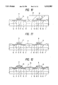
- FIGS. 1 to 14, 19, and 20 are sectional views of an essential part of a semiconductor substrate, showing a manufacturing method for a semiconductor integrated circuit device according to a preferred embodiment of the present invention
- FIGS. 15A, 15B, and 15C are enlarged sectional views of a gate electrode, showing the manufacturing method for the semiconductor integrated circuit device according to the preferred embodiment
- FIGS. 16A and 16B are graphs showing the concentration profiles of n-type impurities in polysilicon films forming the gate electrode
- FIG. 17 is a graph showing the relation between the concentration of an n-type impurity in the interface between a polysilicon film and a Ti silicide layer and the sheet resistance of the gate electrode;
- FIG. 18 is a graph showing the relation between the temperature of second annealing and the sheet resistance of the gate electrode
- FIG. 21 is a graph showing the relation between the temperature of densification of a BPSG film and the sheet resistance of the gate electrode.
- This preferred embodiment is an embodiment applied to a CMISFET (Complementary MISFET) wherein gate electrodes in an n-channel MISFET and a p-channel MISFET are formed of n-type polysilicon films.
- a manufacturing method for the CMISFET will be described with reference to FIGS. 1 to 21.
- a field insulating film 2 for isolating elements is first formed by a known selective oxidation process (LOCOS process) on the principal surface of a semiconductor substrate 1 formed of p-type silicon single crystal, for example.
- LOC process selective oxidation process
- an n-type impurity e.g., phosphorus
- a p-type impurity e.g., boron
- thin gate insulating films 5 of silicon oxide are formed on the principal surfaces of active regions of the n-type well 3 and the p-type well 4.
- a polysilicon film 6 having a thickness of about 100 nm is deposited over the surface of the semiconductor substrate 1 by a CVD (Chemical Vapor Deposition) process.
- an n-type impurity e.g., phosphorus
- a concentration of about 4 ⁇ 10 20 atoms/cm 3 is introduced at a concentration of about 4 ⁇ 10 20 atoms/cm 3 into the polysilicon film 6.
- the concentration of the n-type impurity in the polysilicon film 6 is low, a depletion layer is formed in the gate electrode when a positive voltage is applied to the gate electrode with the p-type well 4 grounded, so that the effective thickness of the gate insulating film is increased to decrease a drain current in the MISFET.
- the n-type impurity is introduced at the concentration of at least about 2 ⁇ 10 20 atoms/cm 3 or more into the polysilicon film 6.
- a polysilicon film 7 having a thickness of about 100 nm is deposited over the surface of the semiconductor substrate 1 by a CVD process. No n-type impurity is introduced into the polysilicon film 7. In the case that an n-type impurity is introduced into the polysilicon film 7, the concentration of the n-type impurity in the polysilicon film 7 is set lower than that in the polysilicon film 6.
- the concentration of the n-type impurity in the polysilicon film 7 is high, a silicide reaction in the interface between the polysilicon film 7 and a Ti film deposited thereon to be hereinafter described is hindered.
- the n-type impurity in the polysilicon film 6 formed under the polysilicon film 7 is somewhat diffused into the polysilicon film 7; therefore, when an n-type impurity is introduced into the polysilicon film 7, the concentration of the n-type impurity in the polysilicon film 7 must be set less than or equal to about 1 ⁇ 10 20 atoms/cm 3 .
- the two polysilicon films 6 and 7 are patterned by dry etching with a photoresist 18 as a mask, for example, to thereby form a gate electrode 8 of the n-channel MISFET on the principal surface of the p-type well 4 and a gate electrode 9 of the p-channel MISFET on the principal surface of the n-type well 3.
- the gate electrodes 8 and 9 are formed so that their gate lengths become 0.3 ⁇ m or less, for example.
- both the gate electrode 8 of the n-channel MISFET and the gate electrode 9 of the p-channel MISFET are constructed of a laminated film consisting of the polysilicon film 6 including a high concentration of n-type impurity and the polysilicon film 7 substantially excluding an n-type impurity or including a low concentration of n-type impurity. Accordingly, the concentration of the n-type impurity in the gate electrodes 8 and 9 is high on the gate oxide film 5 side and low on the surface side.
- an n-type impurity e.g., phosphorus or arsenic
- a photoresist 19 as a mask for covering the n-type well 3, thereby forming n-semiconductor regions 10 on the principal surface of the p-type well 4 on both sides of the gate electrode 8.
- the n - semiconductor regions 10 form a part of a source region and a part of a drain region in the n-channel MISFET.
- a p-type impurity e.g., boron
- a photoresist 20 as a mask for covering the p-type well 4, thereby forming p - semiconductor regions 11 having a low impurity concentration on the principal surface of the n-type well 3 on both sides of the gate electrode 9.
- the p - semiconductor regions 11 form a part of a source region and a part of a drain region in the p-channel MISFET.
- a silicon oxide film is deposited over the surface of the semiconductor substrate 1 by a CVD process, and the silicon oxide film is anisotropically etched by using a reaction ion etching (RIE) process, thereby forming side wall spacers 12 on the side walls of the gate electrode 8 in the n-channel MISFET and the gate electrode 9 in the p-channel MISFET.
- RIE reaction ion etching
- an n-type impurity e.g., arsenic
- a photoresist 21 as a mask for covering the n-type well 3, thereby forming n + semiconductor regions 13 having a high impurity concentration on the principal surface of the p-type well 4 on both sides of the gate electrode 8.
- the n + semiconductor regions 13 form a part of the source region and a part of the drain region in the n-channel MISFET.
- a p-type impurity e.g., boron
- a photoresist 22 as a mask for covering the p-type well 4, thereby forming p + semiconductor regions 14 having a high impurity concentration on the principal surface of the n-type well 3 on both sides of the gate electrode 9.
- the p + semiconductor regions 14 form a part of the source region and a part of the drain region in the p-channel MISFET.
- the source and drain regions 10, 11, 13, and 14 having LDD (Lightly Doped Drain) structures are formed in the n-channel MISFET and the p-channel MISFET.
- the gate insulating films 5 on the n + semiconductor regions 13 (source and drain regions) in the n-channel MISFET and on the p + semiconductor regions 14 (source and drain regions) in the p-channel MISFET are removed by an etching liquid containing hydrofluoric acid, for example, thereby exposing the n + semiconductor regions 13 and the p + semiconductor regions 14.
- natural oxide films on the surfaces of the gate electrodes 8 and 9 are also removed.
- a Ti film 15 is deposited over the surface of the semiconductor substrate 1 by using a sputtering process.
- the thickness of the Ti film 15 is set less than or equal to the half of the thickness (about 100 nm) of the polysilicon film 7.
- the thickness of the Ti film 15 is set to about 40 nm.
- the semiconductor substrate 1 is annealed at a temperature of about 650° to 700° C. in an atmosphere of nitrogen gas (first annealing), thereby causing a silicide reaction in the interfaces between the gate electrodes 8 and 9 and the Ti film 15 and in the interfaces between the source and drain regions (the n + semiconductor regions 13 and the p + semiconductor regions 14) and the Ti film 15 (first silicide reaction) to form Ti silicide layers 16.
- the Ti silicide layers 16 formed above are formed of Ti silicide (TiSi x ; x ⁇ 2) having a sheet resistance (tens of ⁇ /sq). substantially equal to that of polysilicon including an n-type impurity at a high concentration. If the first annealing is performed at a temperature higher than about 700° C., the sheet resistance is further decreased; however, the silicon in the source and drain regions is attracted into the Ti film 15 to form the Ti silicide layers 16 also on the side wall spacers 12, with the result that the gate electrodes 8 and 9 and the source and drain regions (the n + semiconductor regions 13 and the p + semiconductor regions 14) are possibly short-circuited through the Ti silicide layers 16 on the side wall spacers 12.
- the first annealing is performed at a temperature lower than about 650° C.
- the above-mentioned silicide reaction is not enough progressed to cause a problem that the Ti film 15 may be entirely removed in removing an unreacted portion of the Ti film 15 to be hereinafter described.
- an unreacted portion of the Ti film 15 left on the field insulating film 2 and the side wall spacers 12 is removed by wet etching using an ammonia/hydrogen peroxide mixed aqueous solution, for example.
- the semiconductor substrate 1 is annealed again at a temperature of about 850° to 900° C. in an atmosphere of nitrogen gas (second annealing) to further progress the above-mentioned silicide reaction, thereby converting the Ti silicide layer 16 into a Ti silicide layer 17 having a low sheet resistance (second silicide reaction).
- the sheet resistance of the Ti silicide layer 17 formed by the second annealing is 5 to 10 ⁇ /sq., which is lower than the sheet resistance (10 to 15 ⁇ /sq.) of a gate electrode having a polycide structure of a laminated film consisting of a polysilicon film and a high-melting point metal silicide film.
- FIGS. 15A to 15C are enlarged sectional views of the gate electrode 8 or 9, showing a progressed condition of the above-mentioned silicide reaction.
- FIG. 15A shows a condition where the Ti film 15 is deposited on the gate electrode 8 or 9
- FIG. 15B shows a condition where the Ti silicide layer 16 having a high sheet resistance is formed in the interface between the gate electrode 8 or 9 and the Ti film 15 by the first annealing.
- the first annealing causes a portion of the polysilicon film 7 of the gate electrode 8 or 9 on the surface side to be consumed by substantially the same thickness as that of the Ti film 15, thereby forming the Ti silicide film 16.
- FIG. 15C shows a condition where the Ti silicide layer 17 having a low sheet resistance is formed by the second annealing. At this time, the polysilicon film 7 is consumed by the thickness twice that by the first annealing. Accordingly, the thickness l 1 of the polysilicon film 7 must be set twice or more of the thickness l 2 of the Ti film 15 (i.e., 1 ⁇ 2l 2 ).
- FIGS. 16A and 16B are graphs showing the concentration profiles of n-type impurities in the two-layer polysilicon films 6 and 7 forming each of the gate electrodes 8 and 9; and FIG. 17 is a graph showing the relation between the concentration of an n-type impurity (phosphorus and/or arsenic) in the interface between the polysilicon film 7 and the Ti silicide layer and the sheet resistance of the gate electrode 8 or 9.
- n-type impurity phosphorus and/or arsenic
- the n-type impurity in the polysilicon film 6 under the polysilicon film 7 forming each of the gate electrodes 8 and 9 is diffused into the polysilicon film 7 to some extent.
- concentration of the n-type impurity in the interface between the Ti silicide layer 17 and the polysilicon film 7 is less than about 2 ⁇ 10 20 atoms/cm 3
- the second silicide reaction (TiSi x ⁇ TiSi 2 ) by the second annealing is enough progressed to form a TiSi x layer as shown in FIG. 16A, and the sheet resistance becomes less than 4 ⁇ /sq.
- the thickness of the polysilicon film 7 is small and the concentration of the n-type impurity in the interface between the Ti silicide layer 17 and the polysilicon film 7 after the second annealing is greater than about 2 x 10²⁰ atoms/cm 3 , the progress of the second silicide reaction by the second annealing is not enough.
- the Ti silicide layer (TiSi x ) 16 is :Left in the interface as shown in FIG. 16B, and the sheet resistance becomes greater than 10 ⁇ /sq. as shown in FIG. 17.
- the thickness of the polysilicon film 7 must be set so that the concentration of the impurity in the interface between the Ti silicide layer 17 and the polysilicon film 7 after the second annealing becomes less than or equal to 1 ⁇ 10 20 atoms/cm 3 .
- FIG. 18 is a graph showing the relation between the second annealing temperature and the sheet resistance of the gate electrode 8 or 9.
- the second annealing temperature when the second annealing temperature is lower than 800° C. the progress of the second silicide reaction is not enough with the result that the sheet resistance of the gate electrode 8 or 9 becomes greater than 10 ⁇ /sq. Further, when the second annealing temperature is higher than 900° C. there occurs agglomeration in the Ti silicide layer 17 to cause variations in the sheet resistance and a gradual increase in value of the sheet resistance. Accordingly, the second annealing temperature must be set within the range of 800° to 900° C., preferably, 850° to 900° C.
- an insulating film 23 of silicon oxide is deposited over the surface of the semiconductor substrate 1 by a CVD process, and a BPSG (Boro Phospho Silicate Glass) film 24 is deposited on the insulating film 23 by a CVD process.
- the semiconductor substrate 1 is subjected to a densify process at a temperature of about 900° C.
- the densify process allows the phosphorus (P) in the BPSG film 24 to be activated and the BPSG film 24 to trap metals such as Na having an adverse effect on the operation of the MISFET.
- the BPSG film 24 may be replaced by a PSG (Phospho Silicate Glass) film, for example, as an insulating film containing phosphorus (P).
- FIG. 21 shows a graph showing the relation between the densify temperature of the BPSG film 24 and the sheet resistance of the gate electrode 8 or 9.
- the densify temperature of the BPSG film 24 must be set within the range of 850° to 950° C., preferably at about 900° C.
- a wiring 26 of aluminum, tungsten, etc. is formed on the BPSG film 24.
- the second annealing and the densifying of the BPSG film 24 are performed in different steps, these processes may be performed in a single step. That is, after forming the Ti silicide layer 16 having a high sheet resistance on each of the gate electrodes 8 and 9 by the first annealing, the insulating film 23 and the BPSG film 24 are deposited over the surface of the semiconductor substrate 1. Then, the semiconductor substrate 1 is annealed at a temperature of about 900° C. to perform a reduction in sheet resistance of the Ti silicide layer 16 and simultaneously perform the densifying of the BPSG film 24. In this case, the manufacturing steps of the MISFET can be shortened.
- the two-layer polysilicon films 6 and 7 forming each gate electrode are sequentially deposited by a CVD process.
- the polysilicon film 6 containing phosphorus at a high concentration may be deposited to have a thickness of about 150 nm by using monosilane (SiH 4 ) and PH 4 . Thereafter, the supply of PH 4 may be cut to further deposit the nondoped polysilicon film 7 having a thickness of about 150 nm by using only the monosilane.
- the manufacturing method of the present invention is applied to the complementary MISFET wherein the gate electrodes in the n-channel MISFET and the p-channel MISFET are formed from the n-type polysilicon films.
- the present invention may be applied to a dual-gate type complementary MISFET wherein the gate electrode in the n-channel MISFET is formed from a n-type polysilicon film and the gate electrode in the p-channel MISFET is formed from a p-type polysilicon film.
- a nondoped polysilicon film having a thickness of about 100 nm may be deposited over the surface of a semiconductor substrate by a CVD process. Then, an n-type impurity may be introduced into the polysilicon film in the n-channel MISFET and a p-type impurity may be introduced into the polysilicon film in the p-channel MISFET by using a photoresist as a mask. Then, a nondoped polysilicon film having a thickness of about 100 nm may be deposited over the surface of the semiconductor substrate by a CVD process. Then, the two-layer polysilicon films may be patterned to form the gate electrodes.
- a layer of silicide of any other high-melting point metals may be formed.
- the concentration of the n-type impurity in the polysilicon film forming a surface side of the gate electrode in the MISFET is made low to thereby well promote the silicide reaction in the interface between the polysilicon film and the high-melting point metal film deposited thereon. Accordingly, the sheet resistance ( ⁇ s) of the gate electrode can be reduced.
- the concentration of the n-type impurity in the polysilicon film forming a gate insulating film side of the gate electrode in the MISFET is made high to thereby suppress the formation of a depletion layer in the gate electrode. Accordingly, an increase in effective thickness of the gate insulating film can be prevented to thereby prevent a decrease in drain current in the MISFET.
- the sheet resistance (ps) of the n-type gate electrode can be reduced by the effect (1), it is unnecessary to use a MISFET having a p-type gate electrode in a circuit region required to have a low resistance. Accordingly, an integrated circuit can be constructed by only the MISFET having the n-type gate electrode, thereby eliminating the need of a masking step for performing ion implantation of a p-type impurity. As a result, the manufacturing steps can be shortened.
Applications Claiming Priority (4)
| Application Number | Priority Date | Filing Date | Title |
|---|---|---|---|
| JP6-031066 | 1994-03-01 | ||
| JP3106694 | 1994-03-01 | ||
| JP6-313838 | 1994-12-16 | ||
| JP6313838A JPH07297400A (ja) | 1994-03-01 | 1994-12-16 | 半導体集積回路装置の製造方法およびそれにより得られた半導体集積回路装置 |
Publications (1)
| Publication Number | Publication Date |
|---|---|
| US5512502A true US5512502A (en) | 1996-04-30 |
Family
ID=26369514
Family Applications (1)
| Application Number | Title | Priority Date | Filing Date |
|---|---|---|---|
| US08/396,786 Expired - Lifetime US5512502A (en) | 1994-03-01 | 1995-03-01 | Manufacturing method for semiconductor integrated circuit device |
Country Status (3)
| Country | Link |
|---|---|
| US (1) | US5512502A (ko) |
| JP (1) | JPH07297400A (ko) |
| KR (1) | KR100365963B1 (ko) |
Cited By (27)
| Publication number | Priority date | Publication date | Assignee | Title |
|---|---|---|---|---|
| US5620920A (en) * | 1995-03-24 | 1997-04-15 | Deutsche Itt Industries Gmbh | Process for fabricating a CMOS structure with ESD protection |
| US5656546A (en) * | 1995-08-28 | 1997-08-12 | Taiwan Semiconductor Manufacturing Company Ltd | Self-aligned tin formation by N2+ implantation during two-step annealing Ti-salicidation |
| US5668024A (en) * | 1996-07-17 | 1997-09-16 | Taiwan Semiconductor Manufacturing Company | CMOS device structure with reduced risk of salicide bridging and reduced resistance via use of a ultra shallow, junction extension, ion implantation process |
| US5681771A (en) * | 1995-03-22 | 1997-10-28 | Hyundai Electronics Industries Co., Ltd. | Method of manufacturing a LDD transistor in a semiconductor device |
| US5723374A (en) * | 1996-12-27 | 1998-03-03 | Taiwan Semiconductor Manufacturing Company, Ltd. | Method for forming dielectric spacer to prevent poly stringer in stacked capacitor DRAM technology |
| US5750437A (en) * | 1996-01-23 | 1998-05-12 | Nec Corporation | Method of fabricating semiconductor device |
| EP0860863A2 (en) * | 1997-02-25 | 1998-08-26 | Tokyo Electron Limited | A laminated structure of polysilicon and tungsten silicide and a method of forming the same |
| FR2762930A1 (fr) * | 1997-05-02 | 1998-11-06 | Mitsubishi Electric Corp | Dispositif a semiconducteurs ayant une structure de grille du type silicium polycristallin/siliciure et procede de fabrication |
| US5851891A (en) * | 1997-04-21 | 1998-12-22 | Advanced Micro Devices, Inc. | IGFET method of forming with silicide contact on ultra-thin gate |
| US5933741A (en) * | 1997-08-18 | 1999-08-03 | Vanguard International Semiconductor Corporation | Method of making titanium silicide source/drains and tungsten silicide gate electrodes for field effect transistors |
| US5981364A (en) * | 1995-12-06 | 1999-11-09 | Advanced Micro Devices, Inc. | Method of forming a silicon gate to produce silicon devices with improved performance |
| US6017809A (en) * | 1996-12-11 | 2000-01-25 | Kabushiki Kaisha Toshiba | Method of manufacturing semiconductor device |
| US6057215A (en) * | 1995-05-31 | 2000-05-02 | Nec Corporation | Process for forming a refractory metal silicide film having a uniform thickness |
| US6063681A (en) * | 1998-01-13 | 2000-05-16 | Lg Semicon Co., Ltd. | Silicide formation using two metalizations |
| US6087254A (en) * | 1996-07-16 | 2000-07-11 | Micron Technology, Inc. | Technique for elimination of pitting on silicon substrate during gate stack etch |
| US6174762B1 (en) | 1999-03-02 | 2001-01-16 | International Business Machines Corporation | Salicide device with borderless contact |
| US6184079B1 (en) * | 1997-10-31 | 2001-02-06 | Samsung Electronics Co., Ltd. | Method for fabricating a semiconductor device |
| US6214671B1 (en) * | 1998-12-16 | 2001-04-10 | United Microelectronics Corp. | Method of forming dual gate structure |
| US20020011613A1 (en) * | 2000-07-11 | 2002-01-31 | Kabushiki Kaisha Toshiba | Semiconductor device and method for manufacturing the same |
| US6376348B1 (en) * | 1997-09-30 | 2002-04-23 | Siemens Aktiengesellschaft | Reliable polycide gate stack with reduced sheet resistance and thickness |
| US6613673B2 (en) | 1996-07-16 | 2003-09-02 | Micron Technology, Inc. | Technique for elimination of pitting on silicon substrate during gate stack etch |
| US20040023503A1 (en) * | 1996-07-16 | 2004-02-05 | Pai-Hung Pan | Technique for elimination of pitting on silicon substrate during gate stack etch |
| US6740935B2 (en) * | 1995-03-24 | 2004-05-25 | Seiko Instruments Inc. | Semiconductor device |
| US20040225655A1 (en) * | 2000-11-06 | 2004-11-11 | Moulton Gregory Hagan | System and method for unorchestrated determination of data sequences using sticky factoring to determine breakpoints in digital sequences |
| US7078342B1 (en) | 1996-07-16 | 2006-07-18 | Micron Technology, Inc. | Method of forming a gate stack |
| US7427537B2 (en) * | 1997-05-01 | 2008-09-23 | Renesas Technology Corp. | Semiconductor integrated circuit device and method for manufacturing the same |
| US8492899B2 (en) | 2010-10-14 | 2013-07-23 | International Business Machines Corporation | Method to electrodeposit nickel on silicon for forming controllable nickel silicide |
Families Citing this family (2)
| Publication number | Priority date | Publication date | Assignee | Title |
|---|---|---|---|---|
| JP2904341B2 (ja) * | 1996-03-06 | 1999-06-14 | 日本電気株式会社 | 半導体装置およびその製造方法 |
| JP2006339441A (ja) * | 2005-06-02 | 2006-12-14 | Fujitsu Ltd | 半導体装置の製造方法 |
Citations (6)
| Publication number | Priority date | Publication date | Assignee | Title |
|---|---|---|---|---|
| JPS61150216A (ja) * | 1984-12-24 | 1986-07-08 | Hitachi Ltd | 半導体装置の製造方法 |
| US4774204A (en) * | 1987-06-02 | 1988-09-27 | Texas Instruments Incorporated | Method for forming self-aligned emitters and bases and source/drains in an integrated circuit |
| US5081066A (en) * | 1989-04-03 | 1992-01-14 | Hyundai Electronics Industries Co., Ltd. | Method for forming a silicide film used in a semiconductor chip |
| US5192992A (en) * | 1991-06-27 | 1993-03-09 | Samsung Electronics Co., Ltd. | Bicmos device and manufacturing method thereof |
| JPH06140355A (ja) * | 1992-10-26 | 1994-05-20 | Nippon Steel Corp | 半導体装置及びその製造方法 |
| US5341014A (en) * | 1992-01-07 | 1994-08-23 | Matsushita Electric Industrial Co., Ltd. | Semiconductor device and a method of fabricating the same |
-
1994
- 1994-12-16 JP JP6313838A patent/JPH07297400A/ja active Pending
-
1995
- 1995-02-22 KR KR1019950003412A patent/KR100365963B1/ko not_active IP Right Cessation
- 1995-03-01 US US08/396,786 patent/US5512502A/en not_active Expired - Lifetime
Patent Citations (6)
| Publication number | Priority date | Publication date | Assignee | Title |
|---|---|---|---|---|
| JPS61150216A (ja) * | 1984-12-24 | 1986-07-08 | Hitachi Ltd | 半導体装置の製造方法 |
| US4774204A (en) * | 1987-06-02 | 1988-09-27 | Texas Instruments Incorporated | Method for forming self-aligned emitters and bases and source/drains in an integrated circuit |
| US5081066A (en) * | 1989-04-03 | 1992-01-14 | Hyundai Electronics Industries Co., Ltd. | Method for forming a silicide film used in a semiconductor chip |
| US5192992A (en) * | 1991-06-27 | 1993-03-09 | Samsung Electronics Co., Ltd. | Bicmos device and manufacturing method thereof |
| US5341014A (en) * | 1992-01-07 | 1994-08-23 | Matsushita Electric Industrial Co., Ltd. | Semiconductor device and a method of fabricating the same |
| JPH06140355A (ja) * | 1992-10-26 | 1994-05-20 | Nippon Steel Corp | 半導体装置及びその製造方法 |
Cited By (35)
| Publication number | Priority date | Publication date | Assignee | Title |
|---|---|---|---|---|
| US5681771A (en) * | 1995-03-22 | 1997-10-28 | Hyundai Electronics Industries Co., Ltd. | Method of manufacturing a LDD transistor in a semiconductor device |
| US5620920A (en) * | 1995-03-24 | 1997-04-15 | Deutsche Itt Industries Gmbh | Process for fabricating a CMOS structure with ESD protection |
| US6740935B2 (en) * | 1995-03-24 | 2004-05-25 | Seiko Instruments Inc. | Semiconductor device |
| US6057215A (en) * | 1995-05-31 | 2000-05-02 | Nec Corporation | Process for forming a refractory metal silicide film having a uniform thickness |
| US5656546A (en) * | 1995-08-28 | 1997-08-12 | Taiwan Semiconductor Manufacturing Company Ltd | Self-aligned tin formation by N2+ implantation during two-step annealing Ti-salicidation |
| US5981364A (en) * | 1995-12-06 | 1999-11-09 | Advanced Micro Devices, Inc. | Method of forming a silicon gate to produce silicon devices with improved performance |
| US5750437A (en) * | 1996-01-23 | 1998-05-12 | Nec Corporation | Method of fabricating semiconductor device |
| US7078342B1 (en) | 1996-07-16 | 2006-07-18 | Micron Technology, Inc. | Method of forming a gate stack |
| US6087254A (en) * | 1996-07-16 | 2000-07-11 | Micron Technology, Inc. | Technique for elimination of pitting on silicon substrate during gate stack etch |
| US6613673B2 (en) | 1996-07-16 | 2003-09-02 | Micron Technology, Inc. | Technique for elimination of pitting on silicon substrate during gate stack etch |
| US20040023503A1 (en) * | 1996-07-16 | 2004-02-05 | Pai-Hung Pan | Technique for elimination of pitting on silicon substrate during gate stack etch |
| US7115492B2 (en) | 1996-07-16 | 2006-10-03 | Micron Technology, Inc. | Technique for elimination of pitting on silicon substrate during gate stack etch using material in a non-annealed state |
| US7041548B1 (en) | 1996-07-16 | 2006-05-09 | Micron Technology, Inc. | Methods of forming a gate stack that is void of silicon clusters within a metallic silicide film thereof |
| US5668024A (en) * | 1996-07-17 | 1997-09-16 | Taiwan Semiconductor Manufacturing Company | CMOS device structure with reduced risk of salicide bridging and reduced resistance via use of a ultra shallow, junction extension, ion implantation process |
| US6017809A (en) * | 1996-12-11 | 2000-01-25 | Kabushiki Kaisha Toshiba | Method of manufacturing semiconductor device |
| US5723374A (en) * | 1996-12-27 | 1998-03-03 | Taiwan Semiconductor Manufacturing Company, Ltd. | Method for forming dielectric spacer to prevent poly stringer in stacked capacitor DRAM technology |
| US6404021B1 (en) | 1997-02-25 | 2002-06-11 | Tokyo Electron Limited | Laminated structure and a method of forming the same |
| EP0860863A3 (en) * | 1997-02-25 | 1998-10-21 | Tokyo Electron Limited | A laminated structure of polysilicon and tungsten silicide and a method of forming the same |
| EP0860863A2 (en) * | 1997-02-25 | 1998-08-26 | Tokyo Electron Limited | A laminated structure of polysilicon and tungsten silicide and a method of forming the same |
| US6489208B2 (en) | 1997-02-25 | 2002-12-03 | Tokyo Electron Limited | Method of forming a laminated structure to enhance metal silicide adhesion on polycrystalline silicon |
| US5851891A (en) * | 1997-04-21 | 1998-12-22 | Advanced Micro Devices, Inc. | IGFET method of forming with silicide contact on ultra-thin gate |
| US7427537B2 (en) * | 1997-05-01 | 2008-09-23 | Renesas Technology Corp. | Semiconductor integrated circuit device and method for manufacturing the same |
| FR2762930A1 (fr) * | 1997-05-02 | 1998-11-06 | Mitsubishi Electric Corp | Dispositif a semiconducteurs ayant une structure de grille du type silicium polycristallin/siliciure et procede de fabrication |
| US6020610A (en) * | 1997-05-02 | 2000-02-01 | Mitsubishi Denki Kabushiki Kaisha | Semiconductor device and method of manufacturing the same |
| US5933741A (en) * | 1997-08-18 | 1999-08-03 | Vanguard International Semiconductor Corporation | Method of making titanium silicide source/drains and tungsten silicide gate electrodes for field effect transistors |
| US6376348B1 (en) * | 1997-09-30 | 2002-04-23 | Siemens Aktiengesellschaft | Reliable polycide gate stack with reduced sheet resistance and thickness |
| US6184079B1 (en) * | 1997-10-31 | 2001-02-06 | Samsung Electronics Co., Ltd. | Method for fabricating a semiconductor device |
| US6063681A (en) * | 1998-01-13 | 2000-05-16 | Lg Semicon Co., Ltd. | Silicide formation using two metalizations |
| US6214671B1 (en) * | 1998-12-16 | 2001-04-10 | United Microelectronics Corp. | Method of forming dual gate structure |
| US6538295B1 (en) | 1999-03-02 | 2003-03-25 | International Business Machines Corporation | Salicide device with borderless contact |
| US6174762B1 (en) | 1999-03-02 | 2001-01-16 | International Business Machines Corporation | Salicide device with borderless contact |
| US20020011613A1 (en) * | 2000-07-11 | 2002-01-31 | Kabushiki Kaisha Toshiba | Semiconductor device and method for manufacturing the same |
| US6887747B2 (en) | 2000-07-11 | 2005-05-03 | Kabushiki Kaisha Toshiba | Method of forming a MISFET having a schottky junctioned silicide |
| US20040225655A1 (en) * | 2000-11-06 | 2004-11-11 | Moulton Gregory Hagan | System and method for unorchestrated determination of data sequences using sticky factoring to determine breakpoints in digital sequences |
| US8492899B2 (en) | 2010-10-14 | 2013-07-23 | International Business Machines Corporation | Method to electrodeposit nickel on silicon for forming controllable nickel silicide |
Also Published As
| Publication number | Publication date |
|---|---|
| JPH07297400A (ja) | 1995-11-10 |
| KR100365963B1 (ko) | 2003-03-04 |
| KR950034672A (ko) | 1995-12-28 |
Similar Documents
| Publication | Publication Date | Title |
|---|---|---|
| US5512502A (en) | Manufacturing method for semiconductor integrated circuit device | |
| KR100530401B1 (ko) | 저저항 게이트 전극을 구비하는 반도체 장치 | |
| US5658811A (en) | Method of manufacturing a semiconductor device | |
| US4874713A (en) | Method of making asymmetrically optimized CMOS field effect transistors | |
| JP3395263B2 (ja) | 半導体装置およびその製造方法 | |
| US5741725A (en) | Fabrication process for semiconductor device having MOS type field effect transistor | |
| KR100685205B1 (ko) | 고융점 금속 게이트를 갖는 반도체 장치 및 그 제조 방법 | |
| US5521106A (en) | Process for fabricating complementary field effect transistors having a direct contact electrode | |
| JPH1012744A (ja) | 半導体装置の製造方法 | |
| JPH0794731A (ja) | 半導体装置及びその製造方法 | |
| JPH1074846A (ja) | 半導体装置及びその製造方法 | |
| JP3259535B2 (ja) | Nmosトランジスタとpmosトランジスタとを有する半導体装置の製造方法 | |
| JPS61224459A (ja) | 半導体装置およびその製造方法 | |
| JPH098135A (ja) | 半導体装置の製造方法 | |
| JPH0922999A (ja) | Mis型半導体装置及びその製造方法 | |
| JPH1140679A (ja) | 半導体装置およびその製造方法 | |
| JPH06216151A (ja) | 半導体装置及びその製造方法 | |
| JPH0982812A (ja) | 半導体装置の製造方法 | |
| JPH09283636A (ja) | 半導体装置の製造方法及び半導体装置 | |
| JP3394204B2 (ja) | 半導体装置の製造方法及び該方法により形成された半導体装置 | |
| JP2513312B2 (ja) | Mosトランジスタの製造方法 | |
| JPH0897414A (ja) | 半導体装置 | |
| KR100266029B1 (ko) | 반도체장치의 제조방법 | |
| JPH0730108A (ja) | Mis型半導体装置及びその製造方法 | |
| JP3507750B2 (ja) | 半導体装置の製造方法 |
Legal Events
| Date | Code | Title | Description |
|---|---|---|---|
| AS | Assignment |
Owner name: HITACHI, LTD., JAPAN Free format text: ASSIGNMENT OF ASSIGNORS INTEREST;ASSIGNORS:OOTSUKA, FUMIO;NONAKA, YUSUKE;AOKI, ATSUMI;REEL/FRAME:007721/0262 Effective date: 19950130 |
|
| STCF | Information on status: patent grant |
Free format text: PATENTED CASE |
|
| FEPP | Fee payment procedure |
Free format text: PAYOR NUMBER ASSIGNED (ORIGINAL EVENT CODE: ASPN); ENTITY STATUS OF PATENT OWNER: LARGE ENTITY |
|
| FPAY | Fee payment |
Year of fee payment: 4 |
|
| FPAY | Fee payment |
Year of fee payment: 8 |
|
| FPAY | Fee payment |
Year of fee payment: 12 |
|
| AS | Assignment |
Owner name: RENESAS ELECTRONICS CORPORATION, JAPAN Free format text: ASSIGNMENT OF ASSIGNORS INTEREST;ASSIGNOR:HITACHI, LTD.;REEL/FRAME:026109/0528 Effective date: 20110307 |