US10700456B2 - Board-mating connector with reduced coupling height - Google Patents
Board-mating connector with reduced coupling height Download PDFInfo
- Publication number
- US10700456B2 US10700456B2 US16/441,047 US201916441047A US10700456B2 US 10700456 B2 US10700456 B2 US 10700456B2 US 201916441047 A US201916441047 A US 201916441047A US 10700456 B2 US10700456 B2 US 10700456B2
- Authority
- US
- United States
- Prior art keywords
- ground
- signal
- contact
- board
- housing
- Prior art date
- Legal status (The legal status is an assumption and is not a legal conclusion. Google has not performed a legal analysis and makes no representation as to the accuracy of the status listed.)
- Active
Links
- 230000008878 coupling Effects 0.000 title claims abstract description 36
- 238000010168 coupling process Methods 0.000 title claims abstract description 36
- 238000005859 coupling reaction Methods 0.000 title claims abstract description 36
- 238000003780 insertion Methods 0.000 claims abstract description 107
- 230000037431 insertion Effects 0.000 claims abstract description 107
- 239000002184 metal Substances 0.000 claims abstract description 14
- 238000005452 bending Methods 0.000 claims description 16
- 230000000694 effects Effects 0.000 description 23
- 239000004020 conductor Substances 0.000 description 1
Images


Classifications
-
- H—ELECTRICITY
- H01—ELECTRIC ELEMENTS
- H01R—ELECTRICALLY-CONDUCTIVE CONNECTIONS; STRUCTURAL ASSOCIATIONS OF A PLURALITY OF MUTUALLY-INSULATED ELECTRICAL CONNECTING ELEMENTS; COUPLING DEVICES; CURRENT COLLECTORS
- H01R12/00—Structural associations of a plurality of mutually-insulated electrical connecting elements, specially adapted for printed circuits, e.g. printed circuit boards [PCB], flat or ribbon cables, or like generally planar structures, e.g. terminal strips, terminal blocks; Coupling devices specially adapted for printed circuits, flat or ribbon cables, or like generally planar structures; Terminals specially adapted for contact with, or insertion into, printed circuits, flat or ribbon cables, or like generally planar structures
- H01R12/70—Coupling devices
- H01R12/7082—Coupling device supported only by cooperation with PCB
-
- H—ELECTRICITY
- H01—ELECTRIC ELEMENTS
- H01R—ELECTRICALLY-CONDUCTIVE CONNECTIONS; STRUCTURAL ASSOCIATIONS OF A PLURALITY OF MUTUALLY-INSULATED ELECTRICAL CONNECTING ELEMENTS; COUPLING DEVICES; CURRENT COLLECTORS
- H01R12/00—Structural associations of a plurality of mutually-insulated electrical connecting elements, specially adapted for printed circuits, e.g. printed circuit boards [PCB], flat or ribbon cables, or like generally planar structures, e.g. terminal strips, terminal blocks; Coupling devices specially adapted for printed circuits, flat or ribbon cables, or like generally planar structures; Terminals specially adapted for contact with, or insertion into, printed circuits, flat or ribbon cables, or like generally planar structures
- H01R12/50—Fixed connections
- H01R12/51—Fixed connections for rigid printed circuits or like structures
- H01R12/52—Fixed connections for rigid printed circuits or like structures connecting to other rigid printed circuits or like structures
-
- H—ELECTRICITY
- H01—ELECTRIC ELEMENTS
- H01R—ELECTRICALLY-CONDUCTIVE CONNECTIONS; STRUCTURAL ASSOCIATIONS OF A PLURALITY OF MUTUALLY-INSULATED ELECTRICAL CONNECTING ELEMENTS; COUPLING DEVICES; CURRENT COLLECTORS
- H01R12/00—Structural associations of a plurality of mutually-insulated electrical connecting elements, specially adapted for printed circuits, e.g. printed circuit boards [PCB], flat or ribbon cables, or like generally planar structures, e.g. terminal strips, terminal blocks; Coupling devices specially adapted for printed circuits, flat or ribbon cables, or like generally planar structures; Terminals specially adapted for contact with, or insertion into, printed circuits, flat or ribbon cables, or like generally planar structures
- H01R12/70—Coupling devices
- H01R12/7005—Guiding, mounting, polarizing or locking means; Extractors
- H01R12/7011—Locking or fixing a connector to a PCB
- H01R12/7017—Snap means
- H01R12/7023—Snap means integral with the coupling device
-
- H—ELECTRICITY
- H01—ELECTRIC ELEMENTS
- H01R—ELECTRICALLY-CONDUCTIVE CONNECTIONS; STRUCTURAL ASSOCIATIONS OF A PLURALITY OF MUTUALLY-INSULATED ELECTRICAL CONNECTING ELEMENTS; COUPLING DEVICES; CURRENT COLLECTORS
- H01R12/00—Structural associations of a plurality of mutually-insulated electrical connecting elements, specially adapted for printed circuits, e.g. printed circuit boards [PCB], flat or ribbon cables, or like generally planar structures, e.g. terminal strips, terminal blocks; Coupling devices specially adapted for printed circuits, flat or ribbon cables, or like generally planar structures; Terminals specially adapted for contact with, or insertion into, printed circuits, flat or ribbon cables, or like generally planar structures
- H01R12/70—Coupling devices
- H01R12/71—Coupling devices for rigid printing circuits or like structures
- H01R12/712—Coupling devices for rigid printing circuits or like structures co-operating with the surface of the printed circuit or with a coupling device exclusively provided on the surface of the printed circuit
- H01R12/714—Coupling devices for rigid printing circuits or like structures co-operating with the surface of the printed circuit or with a coupling device exclusively provided on the surface of the printed circuit with contacts abutting directly the printed circuit; Button contacts therefore provided on the printed circuit
-
- H—ELECTRICITY
- H01—ELECTRIC ELEMENTS
- H01R—ELECTRICALLY-CONDUCTIVE CONNECTIONS; STRUCTURAL ASSOCIATIONS OF A PLURALITY OF MUTUALLY-INSULATED ELECTRICAL CONNECTING ELEMENTS; COUPLING DEVICES; CURRENT COLLECTORS
- H01R12/00—Structural associations of a plurality of mutually-insulated electrical connecting elements, specially adapted for printed circuits, e.g. printed circuit boards [PCB], flat or ribbon cables, or like generally planar structures, e.g. terminal strips, terminal blocks; Coupling devices specially adapted for printed circuits, flat or ribbon cables, or like generally planar structures; Terminals specially adapted for contact with, or insertion into, printed circuits, flat or ribbon cables, or like generally planar structures
- H01R12/70—Coupling devices
- H01R12/71—Coupling devices for rigid printing circuits or like structures
- H01R12/72—Coupling devices for rigid printing circuits or like structures coupling with the edge of the rigid printed circuits or like structures
- H01R12/73—Coupling devices for rigid printing circuits or like structures coupling with the edge of the rigid printed circuits or like structures connecting to other rigid printed circuits or like structures
-
- H—ELECTRICITY
- H01—ELECTRIC ELEMENTS
- H01R—ELECTRICALLY-CONDUCTIVE CONNECTIONS; STRUCTURAL ASSOCIATIONS OF A PLURALITY OF MUTUALLY-INSULATED ELECTRICAL CONNECTING ELEMENTS; COUPLING DEVICES; CURRENT COLLECTORS
- H01R13/00—Details of coupling devices of the kinds covered by groups H01R12/70 or H01R24/00 - H01R33/00
- H01R13/02—Contact members
- H01R13/22—Contacts for co-operating by abutting
- H01R13/24—Contacts for co-operating by abutting resilient; resiliently-mounted
- H01R13/2407—Contacts for co-operating by abutting resilient; resiliently-mounted characterized by the resilient means
- H01R13/2421—Contacts for co-operating by abutting resilient; resiliently-mounted characterized by the resilient means using coil springs
-
- H—ELECTRICITY
- H01—ELECTRIC ELEMENTS
- H01R—ELECTRICALLY-CONDUCTIVE CONNECTIONS; STRUCTURAL ASSOCIATIONS OF A PLURALITY OF MUTUALLY-INSULATED ELECTRICAL CONNECTING ELEMENTS; COUPLING DEVICES; CURRENT COLLECTORS
- H01R13/00—Details of coupling devices of the kinds covered by groups H01R12/70 or H01R24/00 - H01R33/00
- H01R13/40—Securing contact members in or to a base or case; Insulating of contact members
-
- H—ELECTRICITY
- H01—ELECTRIC ELEMENTS
- H01R—ELECTRICALLY-CONDUCTIVE CONNECTIONS; STRUCTURAL ASSOCIATIONS OF A PLURALITY OF MUTUALLY-INSULATED ELECTRICAL CONNECTING ELEMENTS; COUPLING DEVICES; CURRENT COLLECTORS
- H01R13/00—Details of coupling devices of the kinds covered by groups H01R12/70 or H01R24/00 - H01R33/00
- H01R13/46—Bases; Cases
-
- H—ELECTRICITY
- H01—ELECTRIC ELEMENTS
- H01R—ELECTRICALLY-CONDUCTIVE CONNECTIONS; STRUCTURAL ASSOCIATIONS OF A PLURALITY OF MUTUALLY-INSULATED ELECTRICAL CONNECTING ELEMENTS; COUPLING DEVICES; CURRENT COLLECTORS
- H01R13/00—Details of coupling devices of the kinds covered by groups H01R12/70 or H01R24/00 - H01R33/00
- H01R13/648—Protective earth or shield arrangements on coupling devices, e.g. anti-static shielding
- H01R13/652—Protective earth or shield arrangements on coupling devices, e.g. anti-static shielding with earth pin, blade or socket
-
- H—ELECTRICITY
- H01—ELECTRIC ELEMENTS
- H01R—ELECTRICALLY-CONDUCTIVE CONNECTIONS; STRUCTURAL ASSOCIATIONS OF A PLURALITY OF MUTUALLY-INSULATED ELECTRICAL CONNECTING ELEMENTS; COUPLING DEVICES; CURRENT COLLECTORS
- H01R13/00—Details of coupling devices of the kinds covered by groups H01R12/70 or H01R24/00 - H01R33/00
- H01R13/648—Protective earth or shield arrangements on coupling devices, e.g. anti-static shielding
- H01R13/658—High frequency shielding arrangements, e.g. against EMI [Electro-Magnetic Interference] or EMP [Electro-Magnetic Pulse]
- H01R13/6591—Specific features or arrangements of connection of shield to conductive members
- H01R13/6594—Specific features or arrangements of connection of shield to conductive members the shield being mounted on a PCB and connected to conductive members
-
- H—ELECTRICITY
- H01—ELECTRIC ELEMENTS
- H01R—ELECTRICALLY-CONDUCTIVE CONNECTIONS; STRUCTURAL ASSOCIATIONS OF A PLURALITY OF MUTUALLY-INSULATED ELECTRICAL CONNECTING ELEMENTS; COUPLING DEVICES; CURRENT COLLECTORS
- H01R24/00—Two-part coupling devices, or either of their cooperating parts, characterised by their overall structure
- H01R24/38—Two-part coupling devices, or either of their cooperating parts, characterised by their overall structure having concentrically or coaxially arranged contacts
- H01R24/40—Two-part coupling devices, or either of their cooperating parts, characterised by their overall structure having concentrically or coaxially arranged contacts specially adapted for high frequency
- H01R24/52—Two-part coupling devices, or either of their cooperating parts, characterised by their overall structure having concentrically or coaxially arranged contacts specially adapted for high frequency mounted in or to a panel or structure
-
- H—ELECTRICITY
- H01—ELECTRIC ELEMENTS
- H01R—ELECTRICALLY-CONDUCTIVE CONNECTIONS; STRUCTURAL ASSOCIATIONS OF A PLURALITY OF MUTUALLY-INSULATED ELECTRICAL CONNECTING ELEMENTS; COUPLING DEVICES; CURRENT COLLECTORS
- H01R2103/00—Two poles
-
- H—ELECTRICITY
- H01—ELECTRIC ELEMENTS
- H01R—ELECTRICALLY-CONDUCTIVE CONNECTIONS; STRUCTURAL ASSOCIATIONS OF A PLURALITY OF MUTUALLY-INSULATED ELECTRICAL CONNECTING ELEMENTS; COUPLING DEVICES; CURRENT COLLECTORS
- H01R24/00—Two-part coupling devices, or either of their cooperating parts, characterised by their overall structure
- H01R24/38—Two-part coupling devices, or either of their cooperating parts, characterised by their overall structure having concentrically or coaxially arranged contacts
- H01R24/40—Two-part coupling devices, or either of their cooperating parts, characterised by their overall structure having concentrically or coaxially arranged contacts specially adapted for high frequency
- H01R24/50—Two-part coupling devices, or either of their cooperating parts, characterised by their overall structure having concentrically or coaxially arranged contacts specially adapted for high frequency mounted on a PCB [Printed Circuit Board]
Definitions
- the present invention relates to a board-mating connector with a reduced coupling height.
- a board-mating connector transmits an RF signal to a board between an upper board and a lower board, which are formed with signal wires, such as printed circuit boards.
- the board-mating connector increases a coupling height between the upper board and the lower board, and thereby, there is a problem that a thickness of a module including the board-mating connector is increased.
- KR 10-2015-0080486 A KR 10-1326296 B1
- KR 10-1408249 B1 KR 10-1855133 B1.
- the present invention is to provide a board-mating connector with a reduced coupling height.
- a board-mating connector with a reduced coupling height includes a signal portion having one side in contact with a signal electrode of a board and to be electrically connected to the signal electrode; a ground portion having one side in contact with a ground electrode of the board to be electrically connected to the ground electrode and having a hollow inside; a housing portion in which a housing insertion hole is formed such that the signal portion and the ground portion are inserted thereinto and in which at least a part of a portion coming into contact with the ground portion is formed of metal; and a dielectric portion which is inserted into the housing insertion hole and is located between the signal portion and the housing portion such that the signal portion is spaced apart from the ground portion and the housing portion.
- the board-mating connector may further include a protrusion bump which is formed to protrude from the housing portion toward an inside of the housing insertion hole; and a hook bump which is formed by reducing a diameter of a lower portion of a dielectric portion to have a shape corresponding to the protrusion bump.
- the ground portion may further include a ground insertion portion which is inserted into the housing insertion hole; a ground elastic portion which upwardly extends from the ground insertion portion and in which at least three slits are formed along a periphery so as to have an elastic force; and a ground contact portion which extends from the ground elastic portion and comes into contact with the ground electrode of the board.
- the board-mating connector may further include an elastic bending portion which is bent from the ground contact portion and extends in a direction opposite to an extension direction of the ground contact portion.
- the board-mating connector may further include an elastic restriction portion which is bent from the elastic bending portion and extends in a direction opposite to an extension direction of the elastic bending portion.
- the ground elastic portion may include a first elastic portion which is bent and extends from the ground insertion portion; and a second elastic portion which is bent and upwardly extends from the first elastic portion.
- An extension direction of the first elastic portion may be perpendicular to an extension direction of the ground insertion portion.
- the board-mating connector may further include a ground switch portion that switches an extension direction of the first elastic portion from an outside to an inside of the ground insertion portion between the ground insertion portion and the first elastic portion.
- the first elastic portion and the second elastic portion may extend inside the ground insertion portion.
- the board-mating connector may further include an insertion protrusion portion which is formed to protrude to an inside on a periphery of the ground insertion portion.
- the board-mating connector may further include a cover portion which is located between the ground portion and the housing insertion hole.
- the board-mating connector may further include a cover fitting portion which is bent outward a lower end of the ground insertion portion and into which a lower end of the cover portion is inserted.
- the signal portion may include a signal body portion in which a body insertion hole having one side opened is formed; a signal contact portion in which a contact insertion hole having the other side opened is formed; and a signal spring which is inserted between the one side of the body insertion hole and the other side of the contact insertion hole. A part of one side of the signal contact portion may be inserted into the body insertion hole. In a state where the signal spring is compressed, an outside of the signal contact portion may come into contact with an inside of the signal body portion so as to electrically connect the signal body portion to the signal contact portion.
- the board-mating connector may further include a contact protrusion portion which is formed to protrude from an outer wall of the other end of the signal contact portion; and at least three contact slits which are elongated toward one side from the other side of the signal contact portion and are formed along a periphery of the signal contact portion.
- the board-mating connector may further include a body protrusion portion which is formed to protrude from an inner wall of the signal body portion; and a contact groove formed in an annular shape along a periphery of the signal contact portion such that an up-and-down movement of the signal contact portion is guided by inserting the body protrusion portion into the contact groove, when the signal spring is compressed and recovered.
- a coupling height may be reduced, and thereby, there is an effect that a thickness of a module to which a board-mating connector is applied is reduced.
- a hook bump is hooked on a protrusion bump to limit a depth of insertion of a board-mating connector into a housing insertion hole, and thus, there is an effect that a gap between an end of a signal portion and a signal electrode coming into contact with the one end is adjusted.
- an elastic bending portion is formed to prevent a ground electrode from directly coming into contact with an end of a ground contact portion, a ground electrode is prevented from being damaged, and further, an elastic force is improved.
- a first elastic portion and a second elastic portion disperse a stress applied to a ground elastic portion, and thus, there is an effect that a ground portion is prevented from being deformed.
- a first elastic portion and a second elastic portion disperse a stress applied to a ground elastic portion, and thus, there is an effect that a ground portion is prevented from being deformed.
- a signal portion according to the present invention has an effect that PIMD characteristics are improved.
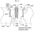
- FIG. 1 is a sectional view illustrating a first embodiment according to the present invention.
- FIG. 2 is a sectional view illustrating a second embodiment according to the present invention.
- FIG. 3 is a sectional view illustrating a third embodiment according to f the present invention.
- FIG. 4 is a perspective view illustrating the third embodiment according to the present invention.
- FIG. 5 is a sectional view illustrating a fourth embodiment according to the present invention.
- FIG. 6 is a perspective view illustrating the fourth embodiment according to the present invention.
- FIG. 7 is a sectional view illustrating a fifth embodiment according to the present invention.
- FIG. 8 is a perspective view illustrating the fifth embodiment according to the present invention.
- FIG. 9 is a sectional view illustrating a signal portion according to the present invention.
- FIG. 10 is a cross-sectional view illustrating a compressed state of the signal portion according to the present invention.
- the first embodiment is characterized in that a dielectric portion 300 is spaced apart from a ground portion 200 and is located between a signal portion 100 and a housing portion 400 .
- second to fifth embodiments are characterized in that the dielectric portion 300 is located between the signal portion 100 and the ground portion 200 .
- first to fifth embodiments are characterized in that the embodiments are each distinguished according to a shape of the ground portion 200 .
- a ground elastic portion 220 includes a first elastic portion 221 and a second elastic portion 222 in the second to fifth embodiments, the second embodiment further includes an elastic restriction portion 250 , and the fourth embodiment further includes a ground switch portion 260 .
- ground elastic portion 220 extends to the outside of the ground insertion portion 210 in the first to third embodiments, and the ground elastic portion 220 extends to an inside of the ground insertion portion 210 in the fourth and fifth embodiments.
- the third and fourth embodiments further include a cover portion 500 .
- an example similar to the embodiment described above may be derived by a combination of elements which will be described below, or a new embodiment may be derived by adding an element to or removing the element from the above-described embodiment.
- the board-mating connector increases a coupling height between an upper board and a lower board, there is a problem that a thickness of a module including the board-mating connector is increased.
- the board-mating connector with a reduced coupling height includes the signal portion 100 , the ground portion 200 , the housing portion 400 , the housing insertion hole 410 , and the dielectric portion 300 as illustrated in FIGS. 1 to 8 .
- One side of the signal portion 100 is in contact with a signal electrode of the board and is electrically connected to the signal electrode.
- ground portion 200 is in contact with a ground electrode of the board and is electrically connected to the ground electrode, and a hollow is formed inside.
- ground portion 200 may be formed by bending a metal plate into a cylindrical shape instead of metal processing.
- the housing insertion hole 410 is formed in the housing portion 400 such that the signal portion 100 and the ground portion 200 are inserted.
- the entire portion in contact with the ground portion 200 is formed of metal, or at least a part of the portion in contact with the ground portion 200 is formed of metal.
- the metal may be electrically connected to the ground portion 200 by selecting a conductive material as the metal.
- the dielectric portion 300 is inserted into the housing insertion hole 410 and is located between the signal portion 100 and the housing portion 400 such that the signal portion 100 is spaced apart from the ground portion 200 and the housing portion 400 .
- the dielectric portion 300 may be spaced apart from the ground portion 200 and be located between the signal portion 100 and the housing portion 400 as illustrated in FIG. 1 , or may be located between the signal portion 100 and the housing portion 400 as illustrated in FIGS. 2 to 8 .
- the housing insertion hole 410 is formed in the housing portion 400 and the board-mating connector is inserted into the housing insertion hole 410 , a coupling height may be reduced, and thereby, there is an effect that a thickness of a module to which the board-mating connector is applied is reduced.
- the board-mating connector with a reduced coupling height further includes a hook bump 301 and a protrusion bump 411 as illustrated in FIGS. 1 to 8 .
- the protrusion bump 411 is formed to protrude from the housing portion 400 to the inside of the housing insertion hole 410 .
- the hook bump 301 formed by reducing a diameter of a lower portion of the dielectric portion 300 has a shape corresponding to the protrusion bump 411 .
- the board-mating connector may swing as illustrated in FIGS. 2 to 8 .
- the ground portion 200 is formed only on the outer side of an upper portion of the dielectric portion 300 with the hook bump 301 as the center and is not formed on the outer side of a lower portion of the dielectric portion 300 , and thus, it is preferable that the dielectric portion 300 is in direct face-to-face contact with the housing portion 400 .
- the hook bump 301 is hooked on the protrusion bump 411 to limit a depth of the housing insertion hole 410 into which the board-mating connector is inserted, and thus, there is an effect that a gap between an end of the signal portion 100 and a signal electrode coming into contact with the one end is adjusted.
- the ground portion 200 of the board-mating connector with a reduced coupling height further includes a ground insertion portion 210 , the ground elastic portion 220 , and a ground contact portion 230 as illustrated in FIGS. 1 to 8 .
- the ground insertion portion 210 is inserted into the housing insertion hole 410 .
- the ground elastic portion 220 upwardly extends from the ground insertion portion 210 , and at least three slits are formed along a periphery so as to have an elastic force.
- the ground elastic portion 220 is divided into three or more portions by the slits and is elastic when coming into contact with the ground electrode.
- the ground contact portion 230 extends from the ground elastic portion 220 and is in contact with the ground electrode of the board.
- the board-mating connector with a reduced coupling height according to the present invention further includes an elastic bending portion 240 as illustrated in FIGS. 2 to 8 .
- the elastic bending portion 240 is bent from the ground contact portion 230 and extends in a direction opposite to the extension direction of the ground contact portion 230 .
- the elastic bending portion 240 is formed to prevent the ground electrode from directly coming into contact with the end of the ground contact portion 230 , the ground electrode is prevented from being damaged, and further, the elastic force is improved.
- ground portion 200 may be deformed if an excessive force is applied to the ground portion 200 .
- the board-mating connector with a reduced coupling height according to the present invention further includes an elastic restriction portion 250 as illustrated in FIG. 2 .
- the elastic restriction portion 250 is bent from the elastic bending portion 240 and extends in a direction opposite to the extension direction of the elastic bending portion 240 .
- the elastic restriction portion 250 comes closer to the ground elastic portion 220 , and if an excessive force is applied to the ground portion 200 , the elastic restriction portion 250 comes into contact with the ground elastic portion 220 , and thereby, deformation of the ground elastic portion 220 is restricted.
- the elastic restriction portion 250 is prevented from being deformed further due to contact with other structures, and thus, there is an effect that the ground portion 200 is prevented from being deformed.
- the ground elastic portion 220 of the board-mating connector with a reduced coupling height may further include a first elastic portion 221 and a second elastic portion 222 as illustrated in FIGS. 2 to 8 .
- the first elastic portion 221 is bent and extends from the ground insertion portion 210 .
- the second elastic portion 222 is bent and upwardly extends from the first elastic portion 221 .
- the first elastic portion 221 and the second elastic portion 222 disperse a stress applied to the ground elastic portion 220 , and thus, there is an effect that the ground portion 200 is prevented from being deformed.
- an extension direction of the first elastic portion 221 may be formed perpendicular to the extension direction of the ground insertion portion 210 .
- the first elastic portion 221 and the second elastic portion 222 extend to the inside of the ground insertion portion 210 such that the ground portion 200 extends in a vertical direction in general, or the ground portion 200 may further include a ground switch portion 260 such that the ground portion 200 extends in a vertical direction in general as illustrated in FIGS. 5 and 6 .
- the ground switch portion 260 switches the extension direction of the first elastic portion 221 from the outside to the inside of the ground insertion portion 210 between the ground insertion portion 210 and the first elastic portion 221 .
- the ground switch portion 260 extends from the ground insertion portion 210 and is bent so as to be perpendicular to the ground insertion portion 210 , extends in a direction opposite to the extension direction, and is switched from the outside to the inside of the first elastic portion 221 .
- the first elastic portion 221 and the second elastic portion 222 disperse the stress applied to the ground elastic portion 220 , there is an effect that the ground portion 200 is prevented from being deformed.
- the board-mating connector with a reduced coupling height according to the present invention further includes an insertion protrusion portion 211 as illustrated in FIGS. 2, 7, and 8 .
- the insertion protrusion portion 211 is formed to protrude from the ground insertion portion 210 toward the inside.
- the insertion protrusion portion 211 is in close contact with a housing to minimize a free space between the ground portion 200 and the housing, there is an effect that the board-mating connector may be prevented from swinging.
- the board-mating connector with a reduced coupling height according to the present invention further includes a cover portion 500 as illustrated in FIGS. 3 to 6 .
- the cover portion 500 is located between the ground portion 200 and the housing insertion hole 410 .
- a cover fitting portion 212 is bent outward at a lower end of the ground insertion portion 210 , and thereby, a lower end of the cover portion 500 is inserted thereinto.
- One or more the cover fitting portions 212 are formed along a periphery of the lower end of the ground insertion portion 210 , make an outer surface of the ground insertion portion 210 come into close contact with an inner surface of the cover portion 500 , and make the cover portion 500 be spaced apart from the housing insertion hole 410 .
- the ground portion 200 may be damaged when being inserted into the housing insertion hole 410 because the ground portion 200 is thin.
- the cover portion 500 surrounds the outside of the ground portion 200 to reinforce a thin thickness of the ground portion 200 , thereby, preventing the ground portion 200 from being damaged when the ground portion 200 is inserted into the housing insertion hole 410 .
- the cover portion 500 surrounds the outside of the ground portion 200 , there is an effect that the board-mating connector is prevented from being damaged when the ground portion 200 is inserted into the housing insertion hole 410 .
- the signal portion 100 of the board-mating connector with a reduced coupling height further includes the signal body portion 110 , the signal contact portion 120 , the contact protrusion portion 122 , a contact slit 123 , a body protrusion portion 112 , and a contact groove 124 as illustrated in FIGS. 9 and 10 .
- a body insertion hole 111 in which one side thereof is opened is formed inside the signal body portion 110 .
- a contact insertion hole 121 in which the other side thereof is opened is formed inside the signal contact portion 120 .
- the signal spring 130 is inserted between the one side of the body insertion hole 111 and the other side of the contact insertion hole 121 .
- a part of one side of the signal contact portion 120 is inserted into the body insertion hole 111 ,
- the outside of the signal contact portion 120 comes into contact with the inside of the signal body portion 110 , and thereby, the signal body portion 110 is electrically connected to the signal contact portion 120 .
- the contact protrusion portion 122 is formed to protrude from an outer wall of the other end of the signal contact portion 120 .
- the contact slit 123 is elongated from one end to the other end of the signal contact portion 120 , and at least three contact slits 123 are formed along a periphery of the signal contact portion 120 .
- the body protrusion portion 112 is formed to protrude from an inner wall of the signal body portion 110 .
- the contact groove 124 is formed in an annular shape along a periphery of the signal contact portion 120 such that an up-and-down movement of the signal contact portion 120 is guided by inserting the body protrusion portion 112 into the contact groove 124 , when the signal spring 130 is compressed and recovered.
- the signal portion 100 since the signal body portion 110 and the signal contact portion 120 are electrically connected to each other, the signal portion 100 according to the present invention has an effect that PIMD characteristics are improved.
- Reference Signs List 100 signal portion 110 signal body portion 111 body insertion hole 112 body protrusion portion 120 signal contact portion 121 contact insertion hole 122 contact protrusion portion 123 contact slit 124 contact groove 130 signal spring 200 ground portion 210 ground insertion portion 211 insertion protrusion portion 212 cover fitting portion 220 ground elastic portion 221 first elastic portion 222 second elastic portion 230 ground contact portion 240 elastic bending portion 250 elastic restriction portion 260 ground switch portion 300 dielectric portion 301 hook bump 400 housing portion 410 housing insertion hole 411 protrusion bump 500 cover portion
Landscapes
- Coupling Device And Connection With Printed Circuit (AREA)
- Details Of Connecting Devices For Male And Female Coupling (AREA)
Priority Applications (1)
| Application Number | Priority Date | Filing Date | Title |
|---|---|---|---|
| US16/862,601 US10790604B2 (en) | 2018-07-10 | 2020-04-30 | Board-mating connector with reduced coupling height |
Applications Claiming Priority (4)
| Application Number | Priority Date | Filing Date | Title |
|---|---|---|---|
| KR20180080103 | 2018-07-10 | ||
| KR10-2018-0080103 | 2018-07-10 | ||
| KR10-2018-0089973 | 2018-08-01 | ||
| KR1020180089973A KR101974785B1 (ko) | 2018-07-10 | 2018-08-01 | 결합 높이가 감소된 기판 메이팅 커넥터 |
Related Child Applications (1)
| Application Number | Title | Priority Date | Filing Date |
|---|---|---|---|
| US16/862,601 Continuation US10790604B2 (en) | 2018-07-10 | 2020-04-30 | Board-mating connector with reduced coupling height |
Publications (2)
| Publication Number | Publication Date |
|---|---|
| US20200021049A1 US20200021049A1 (en) | 2020-01-16 |
| US10700456B2 true US10700456B2 (en) | 2020-06-30 |
Family
ID=66581587
Family Applications (2)
| Application Number | Title | Priority Date | Filing Date |
|---|---|---|---|
| US16/441,047 Active US10700456B2 (en) | 2018-07-10 | 2019-06-14 | Board-mating connector with reduced coupling height |
| US16/862,601 Active US10790604B2 (en) | 2018-07-10 | 2020-04-30 | Board-mating connector with reduced coupling height |
Family Applications After (1)
| Application Number | Title | Priority Date | Filing Date |
|---|---|---|---|
| US16/862,601 Active US10790604B2 (en) | 2018-07-10 | 2020-04-30 | Board-mating connector with reduced coupling height |
Country Status (5)
| Country | Link |
|---|---|
| US (2) | US10700456B2 (de) |
| EP (1) | EP3595093B1 (de) |
| JP (1) | JP6778298B2 (de) |
| KR (1) | KR101974785B1 (de) |
| CN (1) | CN110190444B (de) |
Families Citing this family (9)
| Publication number | Priority date | Publication date | Assignee | Title |
|---|---|---|---|---|
| WO2020099375A1 (en) * | 2018-11-12 | 2020-05-22 | Huber+Suhner Ag | Printed circuit board connector |
| KR102013690B1 (ko) * | 2018-11-23 | 2019-08-23 | 주식회사 기가레인 | 하우징 일체형 기판 메이팅 커넥터 및 이의 제작 방법 |
| CN110854632B (zh) * | 2019-10-09 | 2021-03-23 | 中航光电科技股份有限公司 | 一种同轴连接器及连接器组件 |
| KR102163379B1 (ko) | 2019-12-27 | 2020-10-08 | 주식회사 기가레인 | 기판 메이팅 커넥터 |
| KR20210083814A (ko) * | 2019-12-27 | 2021-07-07 | 주식회사 기가레인 | 기판 메이팅 커넥터 |
| CN111224255B (zh) * | 2020-01-09 | 2021-09-17 | 深圳三星通信技术研究有限公司 | 导体连接件及具有其的射频连接器 |
| CN111541072B (zh) | 2020-03-31 | 2021-10-26 | 深圳三星通信技术研究有限公司 | 一种测试转接器 |
| EP4156420A4 (de) * | 2020-12-21 | 2024-07-24 | Gigalane Co Ltd | Plattensteckverbinder und plattenverbindungsanordnung damit |
| US20240250485A1 (en) * | 2021-07-06 | 2024-07-25 | Rosenberger Hochfrequenztechnik Gmbh & Co. Kg | Contact Sleeve, Connection Arrangement, Signal Transmission System, and Method for Producing a Connection Arrangement |
Citations (16)
| Publication number | Priority date | Publication date | Assignee | Title |
|---|---|---|---|---|
| JPH0555481U (ja) | 1991-12-26 | 1993-07-23 | 第一電子工業株式会社 | 同軸多心コネクタ |
| JPH07336115A (ja) | 1994-06-08 | 1995-12-22 | Nec Corp | 接触形高周波信号接続構造 |
| JPH08504056A (ja) | 1993-10-01 | 1996-04-30 | ブアンズ インコーポレイテッド | プリント基板用の柔軟な積重ね型コネクタ |
| JPH08236227A (ja) | 1995-02-27 | 1996-09-13 | Yokowo Co Ltd | 同軸基板間コネクタ |
| JPH08335483A (ja) | 1995-01-11 | 1996-12-17 | Whitaker Corp:The | パネル取付型同軸コネクタ |
| US5928000A (en) * | 1998-10-07 | 1999-07-27 | Ericsson Inc. | Axially-compliant coaxial connectors and radiotelephones including the same |
| US6231352B1 (en) * | 1999-02-11 | 2001-05-15 | Radiall | Coaxial coupling for interconnecting two printed circuit cards |
| US6354855B2 (en) * | 2000-04-07 | 2002-03-12 | Radiall | Coaxial connector |
| US20030060069A1 (en) * | 2001-08-31 | 2003-03-27 | Duquerroy Patrick M. | Coaxial connector for interconnecting printed circuit boards |
| US6607400B1 (en) | 2002-10-22 | 2003-08-19 | Hon Hai Precision Ind. Co., Ltd. | Low profile RF connector assembly |
| US20110254575A1 (en) * | 2008-10-10 | 2011-10-20 | Molex Incorporated | Probe connector |
| US8105092B2 (en) * | 2009-05-06 | 2012-01-31 | Tyco Electronics Corporation | Electrical connector assembly having connectors mounted to a circuit board |
| US8382488B2 (en) * | 2008-12-22 | 2013-02-26 | Molex Incorporated | Coaxial connector |
| US20150270635A1 (en) | 2012-10-29 | 2015-09-24 | Rosenberger Hochfrequenztechnik Gmbh & Co. Kg | Contact element for transmitting high-frequency signals between two circuit boards |
| US9583854B2 (en) * | 2010-05-11 | 2017-02-28 | Molex Japan Co., Ltd. | Connector and semiconductor testing device having the same |
| US10483669B2 (en) * | 2015-09-28 | 2019-11-19 | Radiall | Unitary RF connector for a board-to-board connection and a ganged connector including a plurality of such unitary connector, for a multiple board-to-board connection |
Family Cites Families (24)
| Publication number | Priority date | Publication date | Assignee | Title |
|---|---|---|---|---|
| US6556033B1 (en) * | 1998-07-10 | 2003-04-29 | Nhk Spring Co., Ltd. | Electroconductive contact unit assembly |
| JP4428803B2 (ja) * | 2000-04-17 | 2010-03-10 | 株式会社ヨコオ | 電気的接続装置および接続ユニット |
| US7097460B2 (en) * | 2005-02-01 | 2006-08-29 | Harris Corporation | Coaxial connector |
| US7220134B2 (en) * | 2005-02-24 | 2007-05-22 | Advanced Interconnections Corporation | Low profile LGA socket assembly |
| FR2905528B1 (fr) * | 2006-08-31 | 2008-10-31 | Radiall Sa | Connecteur coaxial pour relier deux cartes de circuit imprime. |
| CN201285866Y (zh) * | 2008-09-30 | 2009-08-05 | 富士康(昆山)电脑接插件有限公司 | 导电端子 |
| CN201397910Y (zh) * | 2009-03-02 | 2010-02-03 | 富士康(昆山)电脑接插件有限公司 | 电连接器 |
| JP2011108445A (ja) * | 2009-11-16 | 2011-06-02 | Hirose Electric Co Ltd | 回路基板用同軸電気コネクタ |
| CN201570615U (zh) * | 2009-11-20 | 2010-09-01 | 富港电子(东莞)有限公司 | 探针式连接器 |
| US8758067B2 (en) * | 2010-06-03 | 2014-06-24 | Hsio Technologies, Llc | Selective metalization of electrical connector or socket housing |
| JP2012042252A (ja) * | 2010-08-16 | 2012-03-01 | Molex Inc | 同軸プローブ |
| CN202042665U (zh) * | 2010-12-23 | 2011-11-16 | 富士康(昆山)电脑接插件有限公司 | 电连接器 |
| CN202503139U (zh) * | 2011-04-01 | 2012-10-24 | 番禺得意精密电子工业有限公司 | 电连接器 |
| CN202564724U (zh) * | 2011-04-08 | 2012-11-28 | 番禺得意精密电子工业有限公司 | 电连接模组及其芯片模块 |
| CN202142680U (zh) * | 2011-07-20 | 2012-02-08 | 实盈电子(东莞)有限公司 | 电连接器端子 |
| KR101326296B1 (ko) | 2012-02-27 | 2013-11-11 | 주식회사 텔콘 | 기판 연결용 알에프 커넥터 |
| CN103311695B (zh) * | 2012-03-07 | 2016-01-20 | 上海莫仕连接器有限公司 | 电连接器及其端子 |
| CN202601910U (zh) * | 2012-04-13 | 2012-12-12 | 番禺得意精密电子工业有限公司 | 电连接器及其端子 |
| KR101408249B1 (ko) | 2012-12-24 | 2014-06-16 | 주식회사 텔콘 | 무선 통신장비용 커넥터 |
| JP5891549B2 (ja) * | 2014-02-06 | 2016-03-23 | ヒロセ電機株式会社 | インピーダンス特性を向上させた同軸コネクタ |
| CN206116672U (zh) * | 2016-09-09 | 2017-04-19 | 立讯精密工业股份有限公司 | 射频连接器 |
| CN206148645U (zh) * | 2016-09-14 | 2017-05-03 | 泰科电子(上海)有限公司 | 连接器 |
| KR101855133B1 (ko) | 2016-11-16 | 2018-05-08 | 주식회사 케이엠더블유 | 적층구조의 mimo 안테나 어셈블리 |
| CN206574884U (zh) * | 2017-01-24 | 2017-10-20 | 泰科电子(上海)有限公司 | 连接器 |
-
2018
- 2018-08-01 KR KR1020180089973A patent/KR101974785B1/ko active IP Right Grant
-
2019
- 2019-05-24 CN CN201910442298.4A patent/CN110190444B/zh active Active
- 2019-06-04 EP EP19178121.0A patent/EP3595093B1/de active Active
- 2019-06-14 US US16/441,047 patent/US10700456B2/en active Active
- 2019-06-27 JP JP2019119229A patent/JP6778298B2/ja active Active
-
2020
- 2020-04-30 US US16/862,601 patent/US10790604B2/en active Active
Patent Citations (18)
| Publication number | Priority date | Publication date | Assignee | Title |
|---|---|---|---|---|
| JPH0555481U (ja) | 1991-12-26 | 1993-07-23 | 第一電子工業株式会社 | 同軸多心コネクタ |
| JPH08504056A (ja) | 1993-10-01 | 1996-04-30 | ブアンズ インコーポレイテッド | プリント基板用の柔軟な積重ね型コネクタ |
| JPH07336115A (ja) | 1994-06-08 | 1995-12-22 | Nec Corp | 接触形高周波信号接続構造 |
| JPH08335483A (ja) | 1995-01-11 | 1996-12-17 | Whitaker Corp:The | パネル取付型同軸コネクタ |
| JPH08236227A (ja) | 1995-02-27 | 1996-09-13 | Yokowo Co Ltd | 同軸基板間コネクタ |
| US5928000A (en) * | 1998-10-07 | 1999-07-27 | Ericsson Inc. | Axially-compliant coaxial connectors and radiotelephones including the same |
| US6231352B1 (en) * | 1999-02-11 | 2001-05-15 | Radiall | Coaxial coupling for interconnecting two printed circuit cards |
| US6354855B2 (en) * | 2000-04-07 | 2002-03-12 | Radiall | Coaxial connector |
| US6758680B2 (en) * | 2000-08-31 | 2004-07-06 | Tyco Electronics Decolletage S.A. | Coaxial connector for interconnecting printed circuit boards |
| US20030060069A1 (en) * | 2001-08-31 | 2003-03-27 | Duquerroy Patrick M. | Coaxial connector for interconnecting printed circuit boards |
| US6607400B1 (en) | 2002-10-22 | 2003-08-19 | Hon Hai Precision Ind. Co., Ltd. | Low profile RF connector assembly |
| US20110254575A1 (en) * | 2008-10-10 | 2011-10-20 | Molex Incorporated | Probe connector |
| US8690583B2 (en) * | 2008-10-10 | 2014-04-08 | Molex Incorporated | Probe connector |
| US8382488B2 (en) * | 2008-12-22 | 2013-02-26 | Molex Incorporated | Coaxial connector |
| US8105092B2 (en) * | 2009-05-06 | 2012-01-31 | Tyco Electronics Corporation | Electrical connector assembly having connectors mounted to a circuit board |
| US9583854B2 (en) * | 2010-05-11 | 2017-02-28 | Molex Japan Co., Ltd. | Connector and semiconductor testing device having the same |
| US20150270635A1 (en) | 2012-10-29 | 2015-09-24 | Rosenberger Hochfrequenztechnik Gmbh & Co. Kg | Contact element for transmitting high-frequency signals between two circuit boards |
| US10483669B2 (en) * | 2015-09-28 | 2019-11-19 | Radiall | Unitary RF connector for a board-to-board connection and a ganged connector including a plurality of such unitary connector, for a multiple board-to-board connection |
Also Published As
| Publication number | Publication date |
|---|---|
| US20200259282A1 (en) | 2020-08-13 |
| EP3595093A3 (de) | 2020-04-15 |
| CN110190444B (zh) | 2021-01-08 |
| CN110190444A (zh) | 2019-08-30 |
| EP3595093B1 (de) | 2023-04-19 |
| EP3595093A2 (de) | 2020-01-15 |
| KR101974785B1 (ko) | 2019-05-02 |
| JP6778298B2 (ja) | 2020-10-28 |
| JP2020009758A (ja) | 2020-01-16 |
| US20200021049A1 (en) | 2020-01-16 |
| US10790604B2 (en) | 2020-09-29 |
Similar Documents
| Publication | Publication Date | Title |
|---|---|---|
| US10700456B2 (en) | Board-mating connector with reduced coupling height | |
| EP3819993B1 (de) | Verbinder mit gelenk mit begrenztem bewegungsbereich | |
| US9620900B2 (en) | Coaxial connector with floating mechanism | |
| US7128607B2 (en) | Socket connector with reliable shielding member | |
| KR20200005646A (ko) | 전기 커넥터 장치 | |
| CN113054472B (zh) | 基板配合连接器 | |
| US7402082B2 (en) | Electrical connector with retaining shell | |
| US6445350B2 (en) | Terminal device for a glass antenna | |
| EP3843217B1 (de) | Leiterplattengegenstecker | |
| KR20190060662A (ko) | 기판연결용 커넥터 | |
| US10530099B2 (en) | Board mating connector including ground unit in which tapered portion is formed | |
| US20020050388A1 (en) | Full compression coaxial cable assembly | |
| US9899751B2 (en) | Electrical connector limiter structure of wire connection terminal | |
| US11855388B2 (en) | Floating electrical connector | |
| US20190020143A1 (en) | Poke-in connector | |
| US7059875B2 (en) | Ground metal fitting and ground structure for jacks of electronic devices | |
| US7168622B2 (en) | Card edge connector | |
| KR102151781B1 (ko) | 기판 지지 구조를 갖는 전자 기기 | |
| JP4274564B2 (ja) | 多極コネクタ | |
| KR20200060249A (ko) | 기판 간 동축 커넥터 | |
| JP2005243474A (ja) | ジャックのアース金具及び電気機器 | |
| KR20170095629A (ko) | C 클립 |
Legal Events
| Date | Code | Title | Description |
|---|---|---|---|
| AS | Assignment |
Owner name: GIGALANE CO., LTD., KOREA, REPUBLIC OF Free format text: ASSIGNMENT OF ASSIGNORS INTEREST;ASSIGNORS:SONG, HWA YOON;SEO, SANG MIN;KIM, EUN JUNG;AND OTHERS;SIGNING DATES FROM 20190603 TO 20190612;REEL/FRAME:049466/0613 |
|
| FEPP | Fee payment procedure |
Free format text: ENTITY STATUS SET TO UNDISCOUNTED (ORIGINAL EVENT CODE: BIG.); ENTITY STATUS OF PATENT OWNER: SMALL ENTITY |
|
| FEPP | Fee payment procedure |
Free format text: ENTITY STATUS SET TO SMALL (ORIGINAL EVENT CODE: SMAL); ENTITY STATUS OF PATENT OWNER: SMALL ENTITY |
|
| STPP | Information on status: patent application and granting procedure in general |
Free format text: NON FINAL ACTION MAILED |
|
| STPP | Information on status: patent application and granting procedure in general |
Free format text: NOTICE OF ALLOWANCE MAILED -- APPLICATION RECEIVED IN OFFICE OF PUBLICATIONS |
|
| STCF | Information on status: patent grant |
Free format text: PATENTED CASE |
|
| MAFP | Maintenance fee payment |
Free format text: PAYMENT OF MAINTENANCE FEE, 4TH YR, SMALL ENTITY (ORIGINAL EVENT CODE: M2551); ENTITY STATUS OF PATENT OWNER: SMALL ENTITY Year of fee payment: 4 |