US10629517B2 - Semiconductor device and fabrication method thereof - Google Patents
Semiconductor device and fabrication method thereof Download PDFInfo
- Publication number
- US10629517B2 US10629517B2 US16/016,682 US201816016682A US10629517B2 US 10629517 B2 US10629517 B2 US 10629517B2 US 201816016682 A US201816016682 A US 201816016682A US 10629517 B2 US10629517 B2 US 10629517B2
- Authority
- US
- United States
- Prior art keywords
- connection terminal
- bus bar
- semiconductor device
- opening
- fusing
- Prior art date
- Legal status (The legal status is an assumption and is not a legal conclusion. Google has not performed a legal analysis and makes no representation as to the accuracy of the status listed.)
- Active
Links
- 239000004065 semiconductor Substances 0.000 title claims abstract description 100
- 238000000034 method Methods 0.000 title description 20
- 238000004519 manufacturing process Methods 0.000 title description 4
- PXHVJJICTQNCMI-UHFFFAOYSA-N Nickel Chemical compound [Ni] PXHVJJICTQNCMI-UHFFFAOYSA-N 0.000 claims description 33
- 239000000463 material Substances 0.000 claims description 25
- 239000010949 copper Substances 0.000 claims description 19
- RYGMFSIKBFXOCR-UHFFFAOYSA-N Copper Chemical compound [Cu] RYGMFSIKBFXOCR-UHFFFAOYSA-N 0.000 claims description 17
- 229910052802 copper Inorganic materials 0.000 claims description 17
- ATJFFYVFTNAWJD-UHFFFAOYSA-N Tin Chemical compound [Sn] ATJFFYVFTNAWJD-UHFFFAOYSA-N 0.000 claims description 16
- 229910052759 nickel Inorganic materials 0.000 claims description 16
- 238000003466 welding Methods 0.000 description 53
- 239000000758 substrate Substances 0.000 description 17
- 239000011135 tin Substances 0.000 description 15
- 230000008569 process Effects 0.000 description 14
- 229910052718 tin Inorganic materials 0.000 description 13
- 230000004048 modification Effects 0.000 description 8
- 238000012986 modification Methods 0.000 description 8
- 238000010521 absorption reaction Methods 0.000 description 5
- 230000000694 effects Effects 0.000 description 4
- 239000000919 ceramic Substances 0.000 description 3
- 230000000052 comparative effect Effects 0.000 description 3
- 230000012447 hatching Effects 0.000 description 3
- 229910052751 metal Inorganic materials 0.000 description 3
- 239000002184 metal Substances 0.000 description 3
- 239000011347 resin Substances 0.000 description 3
- 229920005989 resin Polymers 0.000 description 3
- 229910000679 solder Inorganic materials 0.000 description 3
- 230000004075 alteration Effects 0.000 description 2
- 150000001875 compounds Chemical class 0.000 description 2
- 230000007547 defect Effects 0.000 description 2
- 238000010586 diagram Methods 0.000 description 2
- 230000004927 fusion Effects 0.000 description 2
- 230000001678 irradiating effect Effects 0.000 description 2
- TWNQGVIAIRXVLR-UHFFFAOYSA-N oxo(oxoalumanyloxy)alumane Chemical compound O=[Al]O[Al]=O TWNQGVIAIRXVLR-UHFFFAOYSA-N 0.000 description 2
- 229920006395 saturated elastomer Polymers 0.000 description 2
- 238000007789 sealing Methods 0.000 description 2
- PIGFYZPCRLYGLF-UHFFFAOYSA-N Aluminum nitride Chemical compound [Al]#N PIGFYZPCRLYGLF-UHFFFAOYSA-N 0.000 description 1
- 229910018082 Cu3Sn Inorganic materials 0.000 description 1
- 229910018471 Cu6Sn5 Inorganic materials 0.000 description 1
- 229910005102 Ni3Sn Inorganic materials 0.000 description 1
- 229910005099 Ni3Sn2 Inorganic materials 0.000 description 1
- 229910003306 Ni3Sn4 Inorganic materials 0.000 description 1
- 229910052581 Si3N4 Inorganic materials 0.000 description 1
- 230000008901 benefit Effects 0.000 description 1
- 238000005520 cutting process Methods 0.000 description 1
- 230000005669 field effect Effects 0.000 description 1
- 230000017525 heat dissipation Effects 0.000 description 1
- 238000009413 insulation Methods 0.000 description 1
- 229910044991 metal oxide Inorganic materials 0.000 description 1
- 150000004706 metal oxides Chemical class 0.000 description 1
- 230000003647 oxidation Effects 0.000 description 1
- 238000007254 oxidation reaction Methods 0.000 description 1
- 238000004080 punching Methods 0.000 description 1
- 230000009467 reduction Effects 0.000 description 1
- HQVNEWCFYHHQES-UHFFFAOYSA-N silicon nitride Chemical compound N12[Si]34N5[Si]62N3[Si]51N64 HQVNEWCFYHHQES-UHFFFAOYSA-N 0.000 description 1
Images


Classifications
-
- H—ELECTRICITY
- H01—ELECTRIC ELEMENTS
- H01L—SEMICONDUCTOR DEVICES NOT COVERED BY CLASS H10
- H01L23/00—Details of semiconductor or other solid state devices
- H01L23/48—Arrangements for conducting electric current to or from the solid state body in operation, e.g. leads, terminal arrangements ; Selection of materials therefor
- H01L23/488—Arrangements for conducting electric current to or from the solid state body in operation, e.g. leads, terminal arrangements ; Selection of materials therefor consisting of soldered or bonded constructions
- H01L23/492—Bases or plates or solder therefor
-
- H—ELECTRICITY
- H01—ELECTRIC ELEMENTS
- H01L—SEMICONDUCTOR DEVICES NOT COVERED BY CLASS H10
- H01L21/00—Processes or apparatus adapted for the manufacture or treatment of semiconductor or solid state devices or of parts thereof
- H01L21/02—Manufacture or treatment of semiconductor devices or of parts thereof
- H01L21/04—Manufacture or treatment of semiconductor devices or of parts thereof the devices having potential barriers, e.g. a PN junction, depletion layer or carrier concentration layer
- H01L21/48—Manufacture or treatment of parts, e.g. containers, prior to assembly of the devices, using processes not provided for in a single one of the subgroups H01L21/06 - H01L21/326
- H01L21/4814—Conductive parts
- H01L21/4846—Leads on or in insulating or insulated substrates, e.g. metallisation
- H01L21/4853—Connection or disconnection of other leads to or from a metallisation, e.g. pins, wires, bumps
-
- H—ELECTRICITY
- H01—ELECTRIC ELEMENTS
- H01L—SEMICONDUCTOR DEVICES NOT COVERED BY CLASS H10
- H01L23/00—Details of semiconductor or other solid state devices
- H01L23/34—Arrangements for cooling, heating, ventilating or temperature compensation ; Temperature sensing arrangements
- H01L23/36—Selection of materials, or shaping, to facilitate cooling or heating, e.g. heatsinks
- H01L23/373—Cooling facilitated by selection of materials for the device or materials for thermal expansion adaptation, e.g. carbon
- H01L23/3735—Laminates or multilayers, e.g. direct bond copper ceramic substrates
-
- H—ELECTRICITY
- H01—ELECTRIC ELEMENTS
- H01L—SEMICONDUCTOR DEVICES NOT COVERED BY CLASS H10
- H01L23/00—Details of semiconductor or other solid state devices
- H01L23/48—Arrangements for conducting electric current to or from the solid state body in operation, e.g. leads, terminal arrangements ; Selection of materials therefor
- H01L23/488—Arrangements for conducting electric current to or from the solid state body in operation, e.g. leads, terminal arrangements ; Selection of materials therefor consisting of soldered or bonded constructions
- H01L23/49—Arrangements for conducting electric current to or from the solid state body in operation, e.g. leads, terminal arrangements ; Selection of materials therefor consisting of soldered or bonded constructions wire-like arrangements or pins or rods
-
- H—ELECTRICITY
- H01—ELECTRIC ELEMENTS
- H01L—SEMICONDUCTOR DEVICES NOT COVERED BY CLASS H10
- H01L23/00—Details of semiconductor or other solid state devices
- H01L23/48—Arrangements for conducting electric current to or from the solid state body in operation, e.g. leads, terminal arrangements ; Selection of materials therefor
- H01L23/488—Arrangements for conducting electric current to or from the solid state body in operation, e.g. leads, terminal arrangements ; Selection of materials therefor consisting of soldered or bonded constructions
- H01L23/498—Leads, i.e. metallisations or lead-frames on insulating substrates, e.g. chip carriers
- H01L23/49811—Additional leads joined to the metallisation on the insulating substrate, e.g. pins, bumps, wires, flat leads
-
- H—ELECTRICITY
- H01—ELECTRIC ELEMENTS
- H01L—SEMICONDUCTOR DEVICES NOT COVERED BY CLASS H10
- H01L23/00—Details of semiconductor or other solid state devices
- H01L23/48—Arrangements for conducting electric current to or from the solid state body in operation, e.g. leads, terminal arrangements ; Selection of materials therefor
- H01L23/488—Arrangements for conducting electric current to or from the solid state body in operation, e.g. leads, terminal arrangements ; Selection of materials therefor consisting of soldered or bonded constructions
- H01L23/498—Leads, i.e. metallisations or lead-frames on insulating substrates, e.g. chip carriers
- H01L23/49827—Via connections through the substrates, e.g. pins going through the substrate, coaxial cables
-
- H—ELECTRICITY
- H01—ELECTRIC ELEMENTS
- H01L—SEMICONDUCTOR DEVICES NOT COVERED BY CLASS H10
- H01L23/00—Details of semiconductor or other solid state devices
- H01L23/52—Arrangements for conducting electric current within the device in operation from one component to another, i.e. interconnections, e.g. wires, lead frames
- H01L23/538—Arrangements for conducting electric current within the device in operation from one component to another, i.e. interconnections, e.g. wires, lead frames the interconnection structure between a plurality of semiconductor chips being formed on, or in, insulating substrates
- H01L23/5385—Assembly of a plurality of insulating substrates
-
- H—ELECTRICITY
- H01—ELECTRIC ELEMENTS
- H01L—SEMICONDUCTOR DEVICES NOT COVERED BY CLASS H10
- H01L24/00—Arrangements for connecting or disconnecting semiconductor or solid-state bodies; Methods or apparatus related thereto
- H01L24/01—Means for bonding being attached to, or being formed on, the surface to be connected, e.g. chip-to-package, die-attach, "first-level" interconnects; Manufacturing methods related thereto
-
- H—ELECTRICITY
- H01—ELECTRIC ELEMENTS
- H01L—SEMICONDUCTOR DEVICES NOT COVERED BY CLASS H10
- H01L25/00—Assemblies consisting of a plurality of individual semiconductor or other solid state devices ; Multistep manufacturing processes thereof
- H01L25/03—Assemblies consisting of a plurality of individual semiconductor or other solid state devices ; Multistep manufacturing processes thereof all the devices being of a type provided for in the same subgroup of groups H01L27/00 - H01L33/00, or in a single subclass of H10K, H10N, e.g. assemblies of rectifier diodes
- H01L25/04—Assemblies consisting of a plurality of individual semiconductor or other solid state devices ; Multistep manufacturing processes thereof all the devices being of a type provided for in the same subgroup of groups H01L27/00 - H01L33/00, or in a single subclass of H10K, H10N, e.g. assemblies of rectifier diodes the devices not having separate containers
- H01L25/07—Assemblies consisting of a plurality of individual semiconductor or other solid state devices ; Multistep manufacturing processes thereof all the devices being of a type provided for in the same subgroup of groups H01L27/00 - H01L33/00, or in a single subclass of H10K, H10N, e.g. assemblies of rectifier diodes the devices not having separate containers the devices being of a type provided for in group H01L29/00
- H01L25/072—Assemblies consisting of a plurality of individual semiconductor or other solid state devices ; Multistep manufacturing processes thereof all the devices being of a type provided for in the same subgroup of groups H01L27/00 - H01L33/00, or in a single subclass of H10K, H10N, e.g. assemblies of rectifier diodes the devices not having separate containers the devices being of a type provided for in group H01L29/00 the devices being arranged next to each other
-
- H—ELECTRICITY
- H01—ELECTRIC ELEMENTS
- H01R—ELECTRICALLY-CONDUCTIVE CONNECTIONS; STRUCTURAL ASSOCIATIONS OF A PLURALITY OF MUTUALLY-INSULATED ELECTRICAL CONNECTING ELEMENTS; COUPLING DEVICES; CURRENT COLLECTORS
- H01R4/00—Electrically-conductive connections between two or more conductive members in direct contact, i.e. touching one another; Means for effecting or maintaining such contact; Electrically-conductive connections having two or more spaced connecting locations for conductors and using contact members penetrating insulation
- H01R4/02—Soldered or welded connections
- H01R4/029—Welded connections
-
- H—ELECTRICITY
- H01—ELECTRIC ELEMENTS
- H01R—ELECTRICALLY-CONDUCTIVE CONNECTIONS; STRUCTURAL ASSOCIATIONS OF A PLURALITY OF MUTUALLY-INSULATED ELECTRICAL CONNECTING ELEMENTS; COUPLING DEVICES; CURRENT COLLECTORS
- H01R43/00—Apparatus or processes specially adapted for manufacturing, assembling, maintaining, or repairing of line connectors or current collectors or for joining electric conductors
- H01R43/02—Apparatus or processes specially adapted for manufacturing, assembling, maintaining, or repairing of line connectors or current collectors or for joining electric conductors for soldered or welded connections
- H01R43/0221—Laser welding
-
- H—ELECTRICITY
- H01—ELECTRIC ELEMENTS
- H01L—SEMICONDUCTOR DEVICES NOT COVERED BY CLASS H10
- H01L2224/00—Indexing scheme for arrangements for connecting or disconnecting semiconductor or solid-state bodies and methods related thereto as covered by H01L24/00
- H01L2224/01—Means for bonding being attached to, or being formed on, the surface to be connected, e.g. chip-to-package, die-attach, "first-level" interconnects; Manufacturing methods related thereto
- H01L2224/26—Layer connectors, e.g. plate connectors, solder or adhesive layers; Manufacturing methods related thereto
- H01L2224/28—Structure, shape, material or disposition of the layer connectors prior to the connecting process
- H01L2224/29—Structure, shape, material or disposition of the layer connectors prior to the connecting process of an individual layer connector
- H01L2224/29001—Core members of the layer connector
- H01L2224/29099—Material
- H01L2224/291—Material with a principal constituent of the material being a metal or a metalloid, e.g. boron [B], silicon [Si], germanium [Ge], arsenic [As], antimony [Sb], tellurium [Te] and polonium [Po], and alloys thereof
- H01L2224/29101—Material with a principal constituent of the material being a metal or a metalloid, e.g. boron [B], silicon [Si], germanium [Ge], arsenic [As], antimony [Sb], tellurium [Te] and polonium [Po], and alloys thereof the principal constituent melting at a temperature of less than 400°C
-
- H—ELECTRICITY
- H01—ELECTRIC ELEMENTS
- H01L—SEMICONDUCTOR DEVICES NOT COVERED BY CLASS H10
- H01L2224/00—Indexing scheme for arrangements for connecting or disconnecting semiconductor or solid-state bodies and methods related thereto as covered by H01L24/00
- H01L2224/01—Means for bonding being attached to, or being formed on, the surface to be connected, e.g. chip-to-package, die-attach, "first-level" interconnects; Manufacturing methods related thereto
- H01L2224/26—Layer connectors, e.g. plate connectors, solder or adhesive layers; Manufacturing methods related thereto
- H01L2224/31—Structure, shape, material or disposition of the layer connectors after the connecting process
- H01L2224/32—Structure, shape, material or disposition of the layer connectors after the connecting process of an individual layer connector
- H01L2224/321—Disposition
- H01L2224/32151—Disposition the layer connector connecting between a semiconductor or solid-state body and an item not being a semiconductor or solid-state body, e.g. chip-to-substrate, chip-to-passive
- H01L2224/32221—Disposition the layer connector connecting between a semiconductor or solid-state body and an item not being a semiconductor or solid-state body, e.g. chip-to-substrate, chip-to-passive the body and the item being stacked
- H01L2224/32225—Disposition the layer connector connecting between a semiconductor or solid-state body and an item not being a semiconductor or solid-state body, e.g. chip-to-substrate, chip-to-passive the body and the item being stacked the item being non-metallic, e.g. insulating substrate with or without metallisation
-
- H—ELECTRICITY
- H01—ELECTRIC ELEMENTS
- H01L—SEMICONDUCTOR DEVICES NOT COVERED BY CLASS H10
- H01L2224/00—Indexing scheme for arrangements for connecting or disconnecting semiconductor or solid-state bodies and methods related thereto as covered by H01L24/00
- H01L2224/01—Means for bonding being attached to, or being formed on, the surface to be connected, e.g. chip-to-package, die-attach, "first-level" interconnects; Manufacturing methods related thereto
- H01L2224/26—Layer connectors, e.g. plate connectors, solder or adhesive layers; Manufacturing methods related thereto
- H01L2224/31—Structure, shape, material or disposition of the layer connectors after the connecting process
- H01L2224/33—Structure, shape, material or disposition of the layer connectors after the connecting process of a plurality of layer connectors
- H01L2224/331—Disposition
- H01L2224/3318—Disposition being disposed on at least two different sides of the body, e.g. dual array
- H01L2224/33181—On opposite sides of the body
-
- H—ELECTRICITY
- H01—ELECTRIC ELEMENTS
- H01L—SEMICONDUCTOR DEVICES NOT COVERED BY CLASS H10
- H01L24/00—Arrangements for connecting or disconnecting semiconductor or solid-state bodies; Methods or apparatus related thereto
- H01L24/01—Means for bonding being attached to, or being formed on, the surface to be connected, e.g. chip-to-package, die-attach, "first-level" interconnects; Manufacturing methods related thereto
- H01L24/26—Layer connectors, e.g. plate connectors, solder or adhesive layers; Manufacturing methods related thereto
- H01L24/28—Structure, shape, material or disposition of the layer connectors prior to the connecting process
- H01L24/29—Structure, shape, material or disposition of the layer connectors prior to the connecting process of an individual layer connector
-
- H—ELECTRICITY
- H01—ELECTRIC ELEMENTS
- H01L—SEMICONDUCTOR DEVICES NOT COVERED BY CLASS H10
- H01L24/00—Arrangements for connecting or disconnecting semiconductor or solid-state bodies; Methods or apparatus related thereto
- H01L24/01—Means for bonding being attached to, or being formed on, the surface to be connected, e.g. chip-to-package, die-attach, "first-level" interconnects; Manufacturing methods related thereto
- H01L24/26—Layer connectors, e.g. plate connectors, solder or adhesive layers; Manufacturing methods related thereto
- H01L24/31—Structure, shape, material or disposition of the layer connectors after the connecting process
- H01L24/33—Structure, shape, material or disposition of the layer connectors after the connecting process of a plurality of layer connectors
-
- H—ELECTRICITY
- H01—ELECTRIC ELEMENTS
- H01L—SEMICONDUCTOR DEVICES NOT COVERED BY CLASS H10
- H01L2924/00—Indexing scheme for arrangements or methods for connecting or disconnecting semiconductor or solid-state bodies as covered by H01L24/00
- H01L2924/0001—Technical content checked by a classifier
- H01L2924/00014—Technical content checked by a classifier the subject-matter covered by the group, the symbol of which is combined with the symbol of this group, being disclosed without further technical details
-
- H—ELECTRICITY
- H01—ELECTRIC ELEMENTS
- H01L—SEMICONDUCTOR DEVICES NOT COVERED BY CLASS H10
- H01L2924/00—Indexing scheme for arrangements or methods for connecting or disconnecting semiconductor or solid-state bodies as covered by H01L24/00
- H01L2924/013—Alloys
- H01L2924/014—Solder alloys
-
- H—ELECTRICITY
- H01—ELECTRIC ELEMENTS
- H01L—SEMICONDUCTOR DEVICES NOT COVERED BY CLASS H10
- H01L2924/00—Indexing scheme for arrangements or methods for connecting or disconnecting semiconductor or solid-state bodies as covered by H01L24/00
- H01L2924/10—Details of semiconductor or other solid state devices to be connected
- H01L2924/11—Device type
- H01L2924/12—Passive devices, e.g. 2 terminal devices
- H01L2924/1203—Rectifying Diode
-
- H—ELECTRICITY
- H01—ELECTRIC ELEMENTS
- H01L—SEMICONDUCTOR DEVICES NOT COVERED BY CLASS H10
- H01L2924/00—Indexing scheme for arrangements or methods for connecting or disconnecting semiconductor or solid-state bodies as covered by H01L24/00
- H01L2924/10—Details of semiconductor or other solid state devices to be connected
- H01L2924/11—Device type
- H01L2924/13—Discrete devices, e.g. 3 terminal devices
- H01L2924/1304—Transistor
- H01L2924/1305—Bipolar Junction Transistor [BJT]
- H01L2924/13055—Insulated gate bipolar transistor [IGBT]
-
- H—ELECTRICITY
- H01—ELECTRIC ELEMENTS
- H01L—SEMICONDUCTOR DEVICES NOT COVERED BY CLASS H10
- H01L2924/00—Indexing scheme for arrangements or methods for connecting or disconnecting semiconductor or solid-state bodies as covered by H01L24/00
- H01L2924/10—Details of semiconductor or other solid state devices to be connected
- H01L2924/11—Device type
- H01L2924/13—Discrete devices, e.g. 3 terminal devices
- H01L2924/1304—Transistor
- H01L2924/1306—Field-effect transistor [FET]
- H01L2924/13091—Metal-Oxide-Semiconductor Field-Effect Transistor [MOSFET]
-
- H—ELECTRICITY
- H01—ELECTRIC ELEMENTS
- H01L—SEMICONDUCTOR DEVICES NOT COVERED BY CLASS H10
- H01L2924/00—Indexing scheme for arrangements or methods for connecting or disconnecting semiconductor or solid-state bodies as covered by H01L24/00
- H01L2924/15—Details of package parts other than the semiconductor or other solid state devices to be connected
- H01L2924/151—Die mounting substrate
- H01L2924/153—Connection portion
- H01L2924/1531—Connection portion the connection portion being formed only on the surface of the substrate opposite to the die mounting surface
- H01L2924/15312—Connection portion the connection portion being formed only on the surface of the substrate opposite to the die mounting surface being a pin array, e.g. PGA
Definitions
- the present invention relates to a semiconductor device and a fabrication method thereof.
- Patent Document 1 Japanese Patent Application Publication No. 2014-236150.
- a semiconductor device may include one or more connection terminals, a bus bar, and one or more fusing portions including a jointing portion.
- a connection terminal may be electrically connected to a semiconductor chip.
- There may be an opening on the bus bar.
- the connection terminal may pass through the opening.
- the jointing portion may be provided over an upper surface of the bus bar from an upper part of the connection terminal. As the connection terminal passes through the opening of the bus bar, the upper part thereof may be positioned above the upper surface of the bus bar.
- a fusing portion may have a jointing portion.
- the jointing portion may be provided in a clearance between a side surface of the connection terminal and a side surface of the opening of the bus bar.
- the jointing portion may be a part of the connection terminal that is welded to the bus bar.
- the fusing portion may have a non-jointing portion.
- the non-jointing portion may be positioned opposite to the jointing portion, in a direction orthogonal to a length direction of the connection terminal.
- the non-jointing portion may be a part of the connection terminal that is not welded to the bus bar.
- a length from an upper end of the fusing portion to the upper surface of the bus bar may be 0.1 mm or longer.
- a length from the upper end of the fusing portion to the upper surface of the bus bar may be 0.9 mm or shorter.
- an outline of the connection terminal may partially be in a circular shape.
- a length of an arc defined by a center and a radius of the circular shape of the connection terminal may be between 0.75 mm and 2.50 mm inclusive.
- a sectorial shaped central angle that is defined by the center and the radius of the circular shape of the connection terminal may be between 86 degrees and 287 degrees inclusive.
- a ratio of a diameter of the connection terminal to a diameter of the opening of the bus bar may be between 0.907 and 0.991 inclusive.
- the connection terminal may include a first body part, a first plated layer and a second plated layer.
- the first body part may contain copper material.
- the first plated layer may be provided on a surface of the first body part.
- the first plated layer may contain nickel material.
- the second plated layer may be provided on a surface of the first plated layer.
- the second plated layer may contain tin material.
- connection terminal may include a taper part.
- the taper part may be provided from the upper part of the connection terminal to a predetermined height position in a length direction of the connection terminal.
- connection terminal and the bus bar When the connection terminal and the bus bar are seen from above, the taper part of the connection terminal and a center of the fusing portion may overlap each other.
- one of the one or more fusing portions may be provided to each of the connection terminals.
- the bus bar may have a taper part in its opening. At an edge of a lower surface that is opposite to an upper surface of the bus bar, the taper part may make a diameter of the opening to become small from the lower surface toward the upper surface.
- the semiconductor device may have the fusing portion on the bus bar.
- the fusing portion may be provided off-centered from a center of the connection terminal in a certain direction.
- the semiconductor device may have a plurality of fusing portions on the bus bar.
- the plurality of fusing portions may be provided side by side in a first direction.
- Each of the plurality of fusing portions may be provided off-centered from the center of a connection terminal to the same certain direction in the first direction.
- the semiconductor device may have a first number of the fusing portions and a second number of the fusing portions on the bus bar.
- the first number of the fusing portions may be provided side by side in the first direction.
- the second number of the fusing portions may be provided to be spaced apart from the first number of the fusing portions in a second direction.
- the second number of the fusing portions may also be provided side by side in the first direction.
- the second direction may be orthogonal to the first direction.
- Each of the first number of the fusing portions and each of the second number of the fusing portions may be provided off-centered from a center of a connection terminal to the same certain direction in the first direction.
- the bus bar may include a convex. There may be a connection opening on the convex.
- a connection opening may be a connection opening through which a fixing member to fix the bus bar and an external connection terminal passes.
- a top part of the convex may be positioned above an upper end of the connection terminal.
- the bus bar When the bus bar is seen from above, the bus bar may be in a rectangular shape having a short side and a long side.
- the semiconductor device may have the first number of the fusing portions and the second number of the fusing portions.
- the first number of the fusing portions may be provided on a first side of the convex in a direction parallel with the long side.
- the first number of the fusing portions may be provided side by side in a direction parallel with the short side.
- the second number of the fusing portions may be provided on a second side of the convex in a direction parallel with the long side.
- the second side may be a side that is opposite to the first side.
- the second number of the fusing portions may be provided side by side in a direction parallel with the short side.
- Each of the first number of the fusing portions and each of the second number of the fusing portions may be provided off-centered from a center of a connection terminal to the same certain direction in the short side direction.
- a lower surface of the top part of the convex may be positioned above an upper surface of a flat part of the bus bar other than the convex of the bus bar.
- a fabrication method of the semiconductor device may include, making the connection terminal pass through the opening of the bus bar, and forming the fusing portion.
- the connection terminal may be electrically connected to a semiconductor chip.
- the fusing portion may include the jointing portion.
- the fusing portion may be formed by irradiating the taper part of the connection terminal with laser light, which is positioned above the upper surface of the bus bar.
- a connecting portion may be formed over the upper surface of the bus bar from the upper part of the connection terminal.
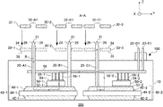
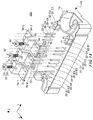
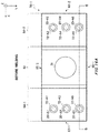
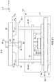
- FIG. 1 is a perspective view illustrating a part of a power semiconductor device 200 in the first embodiment.
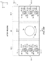
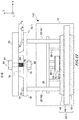
- FIG. 2 is a drawing illustrating a cross section taken along A-A of FIG. 1 .
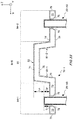
- FIG. 3 is an enlarged cross sectional view of the vicinity of a top part 21 of a connection terminal 20 -A 1 in FIG. 2 before welding.
- FIG. 4 is an experimental result illustrating a relation between protruding length L 1 and tensile strength before welding.
- FIG. 5 is an enlarged drawing of the vicinity of the top part 21 of the connection terminal 20 -A 1 in FIG. 2 in a welding process.
- FIG. 6 is an enlarged drawing of the vicinity of the top part 21 of the connection terminal 20 -A 1 in FIG. 2 after welding.
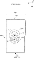
- FIG. 7 is a cross sectional photograph of the connection terminal 20 -A 1 , a bus bar 30 - 1 , and a fusing portion 60 .
- FIG. 8 is a photograph of the connection terminal 20 -A 1 , the bus bar 30 - 1 and the fusing portion 60 taken from above.
- FIG. 9 is an experimental result illustrating a relation between a clearance C between a connection terminal 20 and a bus bar 30 , and length of an arc 124 after welding.
- FIG. 10 is an experimental result illustrating relations between length of arcs 124 and tensile strength after welding.
- FIG. 11 is a cross sectional photograph of a connection terminal 20 -A 1 , a bus bar 30 - 1 , and a fusing portion 60 in a comparative example.
- FIG. 12 is a drawing illustrating a cross section taken along A-A of a power semiconductor device 210 in the second embodiment.
- FIG. 13 is a top view of a bus bar 30 - 1 and one connection terminal 20 -A 1 after welding.
- FIG. 14 is a top view illustrating a first modification example of a bus bar 30 - 1 and a plurality of connection terminals 20 after welding.
- FIG. 15 is a perspective view illustrating a part of a power semiconductor device 220 in the third embodiment.
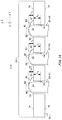
- FIG. 16A is a top view of a bus bar 70 - 1 and connection terminals 20 -A 1 to 20 -A 6 before welding.
- FIG. 16B is a top view of the bus bar 70 - 1 and connection terminals 20 -A 1 to 20 -A 6 after welding.
- FIG. 17 is a drawing illustrating a cross section taken along B-B of FIG. 16A .
- FIG. 18 is a drawing illustrating a cross section taken along C-C of FIG. 16B .
- FIG. 19 is a top view illustrating a first modification example of a bus bar 70 - 1 and one connection terminal 20 after welding.
- FIG. 20 is a drawing illustrating a cross section taken along D-D of FIG. 15 after welding.
- FIG. 21 is a drawing illustrating a cross section taken along D-D of FIG. 15 in a first modification example after welding.
- FIG. 22 is a drawing illustrating a cross section taken along D-D of FIG. 15 in a second modification example after welding.
- FIG. 23 is a drawing illustrating a cross section taken along B-B of FIG. 16A in the fourth embodiment.
- FIG. 1 is a perspective view illustrating a part of a power semiconductor device 200 in the first embodiment.
- the Z axis in the present example is an axis orthogonal to the X axis and the Y axis.
- the X, Y, and Z axes in the present example configure the right-handed system.
- the X, Y, and Z axes are used for indicating relative directions in the power semiconductor device 200 .
- the Z axis direction may not necessarily be parallel with the gravitational direction.
- phrases such as “above” and “below” are used as phrases to indicate directions that are parallel with the Z axis direction, these phrases shall not limit the directions to vertical directions in the gravitational direction either.
- the power semiconductor device 200 may include one or more power semiconductor modules 100 and a plurality of bus bars 30 . Illustrated in FIG. 1 is the power semiconductor device 200 having connection terminals 20 and the bus bars 30 before being welded together. Note that, in FIG. 1 , although one power semiconductor module 100 that is positioned at the end of the +X direction is illustrated, the power semiconductor device 200 may have a plurality of power semiconductor modules 100 that are provided side by side in the X axis direction.
- the power semiconductor module 100 in the present example has so-called 2 in 1 (two-in-one) structure.
- an upper arm and a lower arm may have a power MOSFET (Metal Oxide Semiconductor Field Effect Transistor) semiconductor chip and a FWD (Free Wheeling Diode) semiconductor chip, respectively, which are connected reversely parallel with each other.
- MOSFET Metal Oxide Semiconductor Field Effect Transistor
- FWD Free Wheeling Diode
- the power semiconductor module 100 may have a plurality of connection terminals 20 .
- the power semiconductor module 100 of the present example has a plurality of connection terminals 20 and a plurality of connection terminals 22 respectively protruding from an upper surface of a resin case 10 in +Z direction.
- connection terminals 20 -A 1 and 20 -A 2 are drain terminals
- connection terminals 20 -B 1 and 20 -B 2 are source terminals
- connection terminals 20 -C 1 and 20 -C 2 are output terminals.
- the output terminals may output current to a motor from an electrical contact between a source of the upper arm and a drain of the lower arm, and may be the U-phase (or the V-phase or the W-phase) output terminal in the three-phase inverter circuit.
- connection terminals 20 There may be openings 32 on the bus bars 30 through which the connection terminals 20 pass.
- the openings 32 of the present example are through-openings made in cylindrical shapes.
- the bus bars 30 may serve as conductive members placed between the connection terminals 20 and external connection terminals (not shown), or may also serve as external connection terminals.
- the bus bar 30 - 1 may electrically connect a plurality of drain terminals to each other, and may serve as a connection having drain potential in the power semiconductor module 100 .
- openings 32 -B 1 and 32 -B 2 on a bus bar 30 - 2 which correspond to the connection terminals 20 -B 1 and 20 -B 2 respectively, and the bus bar 30 - 2 may electrically connect a plurality of source terminals to each other.
- the bus bar 30 - 2 may serve as a connection having source potential in the power semiconductor module 100 .
- openings 32 -C 1 and 32 -C 2 on a bus bar 30 - 3 which correspond to the connection terminals 20 -C 1 and 20 -C 2 respectively, and the bus bar 30 - 3 may electrically connect a plurality of output terminals to each other.
- the bus bar 30 - 3 may serve as an output in the power semiconductor module 100 .
- Connection terminals 22 -D 1 and 22 -D 2 may be source sensing terminals for sensing current that flows between the drain and the source.
- Connection terminals 22 -E 1 and 22 -E 2 may be gate terminals for supplying on/off control signals to a gate of the power MOSFET.
- the connection terminals 22 -D 1 and 22 -D 2 may be electrically connected to each other, not by the bus bar 30 but by a wiring substrate (not shown).
- the connection terminals 22 -E 1 and 22 -E 2 may be electrically connected to each other by a wiring substrate (not shown).
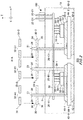
- FIG. 2 is a drawing illustrating a cross section taken along A-A of FIG. 1 .
- the A-A cross section is a cross section parallel with a Y-Z plane that passes through the openings 32 -A 1 , 32 -B 1 , and 32 -C 1 .
- the bus bars 30 being spaced apart above the connection terminals 20 are illustrated with the solid lines, and the bus bars 30 that have been passed through by the connection terminals 20 through their openings 32 are illustrated with the dashed lines.
- illustrated in FIG. 2 is also the power semiconductor device 200 having connection terminals 20 and the bus bars 30 before being welded together.
- the ceramic circuit substrates 40 are one example of an insulation circuit substrate.
- the ceramic circuit substrates 40 of the present example include insulating substrates 44 having any of aluminum oxide (Al 2 O 3 ), aluminum nitride (AlN), silicon nitride (Si 3 n 4 ) and the like, and conductive layers 42 and conductive layers 46 which are in copper (Cu) wiring patterns to contact with upper surfaces and lower surfaces of the insulating substrates 44 respectively.
- the conductive layers 42 to contact with the lower surfaces of the insulating substrates 44 may have functions to emit heat that is generated from the semiconductor chips 50 to the outside of the case 10 .
- the conductive layers 46 to contact with the upper surfaces of the insulating substrates 44 may have functions to electrically connect the semiconductor chips 50 and the connection terminals 20 .
- the semiconductor chips 50 of the present example are power MOSFET semiconductor chips. Drain electrodes of the semiconductor chips 50 may be electrically connected to the conductive layers 46 via the solder layers 52 . Also, source electrodes of the semiconductor chips 50 may be electrically connected to the wiring substrate 58 via the solder layers 54 and the conductive pins 56 .
- the wiring substrate 58 may be a printed wiring substrate having wiring patterns on its upper surface and lower surface. There may be openings on the wiring substrate 58 through which the connection terminals 20 pass.
- the connection terminals 20 may protrude from upper surfaces of the conductive layers 46 to the outside of the case 10 through the openings of the wiring substrate 58 .
- the connection terminals 20 may be electrically connected to the semiconductor chips 50 at least via the conductive layers 46 .
- the semiconductor chip 50 - 1 to serve as the upper arm is turned on, current flows from the connection terminal 20 -A 1 to the connection terminal 20 -C 1 through a conductive layer 46 - 1 , the semiconductor chip 50 - 1 , the conductive pin 56 - 1 , the wiring substrate 58 , and a conductive layer 46 - 2 .
- a flow of current in this case is illustrated with the solid line R.
- the semiconductor chip 50 - 2 to serve as the lower arm is turned on, current flows from the connection terminal 20 -B 1 to the connection terminal 20 -C 1 through the semiconductor chip 50 - 2 etc.
- semiconductor chips 50 in another example may be substituted by IGBT (Insulated Gate Bipolar Transistor) semiconductor chips, instead of the power MOSFET semiconductor chips.
- RC-IGBT Reverse Conducting-IGBT
- semiconductor chips 50 are IGBT semiconductor chips or RC-IGBT semiconductor chips, the source and drain in the description of FIG. 2 may be deemed to be replaced with an emitter and a collector, respectively.
- these semiconductor chips may also be Si semiconductors, or may also be wide bandgap semiconductors such as SiC semiconductors.
- the connection terminals 20 may include taper parts 26 .
- the taper parts 26 may be provided from top parts 21 to predetermined height positions in length directions. Lower ends of the taper parts 26 may have the same diameters as those of the connection terminals 20 .
- the taper parts 26 may have angles between 20 degrees and 80 degrees inclusive, with the Z axis direction as reference. It is advantageous that, by providing the taper parts 26 , work in an assembling process to make the connection terminals 20 pass through the openings 32 becomes easy, compared to a case in which there are no taper parts 26 .
- the bus bars 30 in the present example have upper surfaces 34 and lower surfaces 36 opposite to the upper surfaces 34 .
- the top parts 21 of the connection terminals 20 may be positioned above the upper surfaces 34 .
- the lower ends of the taper parts 26 may be positioned at the same level as the upper surfaces 34 of the bus bars 30 , or above the upper surfaces 34 .
- Parts of the connection terminals 20 positioned above the upper surfaces 34 may be fused by receiving laser light, in order to serve as so-called bonding material that physically and electrically connect the connection terminals 20 and the bus bars 30 .
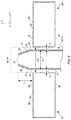
- FIG. 3 is an enlarged cross sectional view of the vicinity of the top part 21 of the connection terminal 20 -A 1 in FIG. 2 before welding.
- FIG. 3 is a cross sectional view parallel with a Y-Z plane that passes through connection terminals 20 and bus bars 30 .
- the connection terminals 20 of the present example include first body parts 23 , first plated layers 24 provided on surfaces of the first body parts 23 , and second plated layers 25 provided on surfaces of the first plated layers 24 .
- the plurality of connection terminals 20 may be continuous terminals rolled into reel shapes and connected in series.
- the continuous terminals of the present example are provided with the first plated layers 24 and the second plated layers 25 , and further provided with the taper parts 26 by punching.
- each connection terminal 20 is formed by sequentially cutting off each of the continuous terminals by a predetermined length.
- the first plated layers 24 and the second plated layers 25 of the present example are provided to the taper parts 26 and circular pillars 27 , but not provided to the top parts 21 .
- the first body parts 23 may contain copper material.
- the copper material may be so-called pure copper.
- the pure copper is, for example, any of Oxygen-Free Copper, Tough-Pitch Copper, and Phosphorous-Deoxidized Copper. It is advantageous that, by forming the first body parts 23 with copper material, electrical resistance of the connection terminals 20 is reduced and high heat dissipation effect can be obtained.
- the first plated layers 24 may contain nickel (Ni) material
- the second plated layers 25 may contain tin (Sn) material.
- absorption efficiency of copper, nickel, and tin with respect to laser light having a wavelength of between 900 nm and 1,100 nm inclusive are approximately 10%, approximately 28%, and approximately 45%, respectively.
- absorption efficiency of laser light irradiated on the connection terminals 20 can be increased compared to a case in which these are not provided.
- tin plated layers on nickel plated layers absorption efficiency of laser light can be increased compared to a case in which nickel plated layers are provided on tin plated layers.
- connection terminals 20 by increasing absorption efficiency of laser light, heat generated by absorption of the laser light is efficiently conveyed to the connection terminals 20 .
- regions of connection terminals 20 to be fused by irradiation of laser light can be secured sufficiently. Once regions of the connection terminals 20 to be fused can be secured sufficiently, fusion bonding area between the fused connection terminals 20 and the bus bars 30 can be secured sufficiently.
- the bus bars 30 in the present example include second body parts 33 containing copper material, and third plated layers 35 containing nickel material or tin material which is provided on surfaces of the second body parts 33 .
- the third plated layers 35 may have laminated structures in which tin plated layers are provided on nickel plated layers.
- the clearance C is distance between a side surface of the circular pillar 27 of the connection terminal 20 and a side surface of the opening 32 of the bus bar 30 . Note that, the length of the connection terminal 20 to protrude from the upper surface 34 of the bus bar 30 is expressed with L 1 .
- FIG. 4 is an experimental result illustrating relations between the protruding length L 1 and tensile strength before welding.
- the horizontal axis indicates the protruding length L 1 [mm] “before” welding.
- the vertical axis indicates tensile strength [N] that illustrates, “after” welding the connection terminals 20 to the bus bars 30 by irradiating laser light on the connection terminals 20 , the strength needed to separate the bus bars 30 and the connection terminals 20 by pulling off the connection terminals 20 downwards from the bus bars 30 .
- the plot with negative L 1 means that the top parts 21 of the connection terminals 20 were arranged below the upper surfaces 34 of the bus bars 30 , and then the connection terminals 20 were welded subsequently.
- the plot with positive L 1 means that the top parts 21 of the connection terminals 20 were arranged above the upper surfaces 34 of the bus bars 30 , and then the connection terminals 20 were welded subsequently.
- because fusing portions are formed by fusing the connection terminals 20 it may mean that the longer the length L 1 becomes, the more quantity of the bonding material used for the connecting portions is.
- the protruding length L 1 before welding may be between 0.2 mm and 1.0 mm inclusive, and more preferably, it may be between 0.3 mm and 0.8 mm inclusive. If the length L 1 is less than 0.2 mm, variation in tensile strength becomes large, and stable quality cannot be obtained in the power semiconductor module 100 . It is considered that, this is due to the protruding length being too short, which results in a shortage of bonding material to be fused by receiving laser light.
- the length L 1 is less than 0.2 mm, because the taper parts 26 are positioned at about the same height as that of the upper surfaces 34 or positioned below the upper surfaces 34 of the bus bars 30 , variation in clearances between the bus bars 30 and the connection terminals 20 can occur. Thereby, reduction in bonding strength between the bus bars 30 and the connection terminals 20 and increase in variation in the bonding strength occur. Compared to this, if the length L 1 is 0.2 mm or longer, stable bonding strength is obtained. Note that, if the length L 1 is 0.3 mm or longer, tensile strength is saturated at approximately 150 N. It is considered that, this is because sufficient bonding material has been obtained for completely covering portions that contribute to bonding.
- connection terminals 20 can be prevented from becoming obstruction of structures to be provided on bus bars 30 .
- tensile stress does not increase in proportion to the protruding length L 1 even if L 1 is made larger than 0.8 mm before welding, the advantage of making L 1 larger than 0.8 mm is small.
- FIG. 5 is an enlarged drawing of the vicinity of the top part 21 of the connection terminal 20 -A 1 in FIG. 2 in a welding process.
- laser light is not irradiated parallel with the Z axis direction toward the top part 21 , but instead, laser light L R is tilted at a predetermined angle from the Z axis direction and irradiated toward the taper part 26 .
- laser light L R may be tilted from the Z axis direction to the +Y direction at a predetermined angle of between 10 degrees and 20 degrees inclusive, and may be irradiated toward the taper part 26 and a side surface of the circular pillar 27 in the +Y direction.
- the laser light L R is tilted at 15 degrees to irradiate. In the present example, the laser light L R is irradiated at one point when seen from above. However, because the laser light L R has a predetermined spread, the laser light L R is also irradiated to the top parts 21 of the connection terminals 20 and the circular pillars 27 . Output of the laser light L R may be between 50 J and 90 J inclusive, and irradiation time may be between 10 ms and 20 ms inclusive. Note that, an exemplary region of the connection terminal 20 to be heated with irradiation of the laser light L R is illustrated with the dashed line.
- a welding mark also referred to as a nugget
- positional variation of a nugget in each connection terminal 20 becomes large. If the positional variation of a nugget becomes large, there is a possibility that intensity variation of the fusing portion also becomes large.
- the protruding length L 1 before welding is too long, the fused material of the connection terminal 20 becomes hard to flow into the clearance C.
- the laser light L R was irradiated toward the connection terminal 20 at the vicinity of the height position of the upper surface 34 of the bus bar 30 , in some cases, a non-fused portion occurred near the top part 21 of the connection terminal 20 and the non-fused portion remained as a foreign matter. From this point also, it is desirable to make the length L 1 1.0 mm or shorter, and more preferably, 0.8 mm or shorter.
- FIG. 6 is an enlarged drawing of the vicinity of the top part 21 of the connection terminal 20 -A 1 in FIG. 2 after welding.
- the outline of the connection terminal 20 before welding is illustrated with the dashed lines.
- an edge part of the connection terminal 20 is fused to flow out on the upper surface 34 , as well as to flow into the clearance C.
- Illustrated with the oblique lines in FIG. 6 is a region of the connection terminal 20 after welding where expanded out from the outline of itself before welding. Note that, needless to say, the range of the connection terminal 20 that is fused by irradiation of the laser light may be wider than the oblique line portion.
- the power semiconductor module 100 after welding has the fusing portions 60 .
- a jointing portion 67 of the fusing portion 60 may be provided over the upper surface 34 of the bus bar 30 from an upper part 28 of the connection terminal 20 after welding.
- the fusing portion 60 may have gentle slope from an upper end 62 to the upper surface 34 .
- the fusing portion 60 has the upper part 28 (i.e., a convex region) with its peak height position being the upper end 62 .
- an atomic percent of nickel to copper may be greater than 0 at % and equal to or less than 50 at %
- an atomic percent of tin to copper may be greater than 0 at % and equal to or less than 50 at %.
- the fusing portion 60 may include one or more kinds of Cu 5 Sn, Cu 3 Sn, and Cu 6 Sn 5 , which are chemical compounds of copper and tin, and may include one or more kinds of Ni 3 Sn, Ni 3 Sn 2 , and Ni 3 Sn 4 , which are chemical compounds of nickel and tin.
- the fusing portion 60 may include the jointing portion 67 which is a part of the connection terminal 20 that is fused and welded to the bus bar 30 , and a non-jointing portion 68 which is a part of the connection terminal 20 that is fused but not welded to the bus bar 30 .
- the oblique line portion is the jointing portion 67 .
- the taper part 26 that is provided from the upper part 28 to a predetermined height position is the non-jointing portion 68 .
- the non-jointing portion 68 of the present example is positioned opposite to the jointing portion 67 in the Y axis direction. In the present example, at the non-jointing portion 68 and below it, a gap 65 is remained where the connection terminal 20 and the bus bar 30 are not bonded.
- the connection terminal 20 is rapidly heated or rapidly cooled down, and accordingly, the connection terminal 20 repeats expanding and contracting to the bus bar 30 .
- circumference of the connection terminal 20 that is seen from above is enclosed with the jointing portion 67 to completely fix the connection terminal 20 and the bus bar 30 in the X-Y plane direction completely, distortion occurs in the fusing portion 60 , which is derived from the power cycle.
- Length from the upper end 62 of the fusing portion 60 to the upper surface 34 after welding is expressed as L 2 . Because length of the connection terminal 20 to be fused by the welding process is approximately between 0.1 mm and 0.2 mm, the length L 2 may be shorter than the protruding length L 1 before welding. If the length L 1 of the connection terminal 20 becomes the length L 2 through the welding process, the length L 2 may be 0.1 mm or longer, or more preferably, it may be 0.2 mm or longer. By making 0.1 mm ⁇ L 2 , 40 N or more tensile strength can be secured, for example.
- the length L 2 after welding may be 0.9 mm or shorter, and more preferably, it may be 0.7 mm or shorter.
- an external connection terminal is further provided on the bus bar 30 , and once the external connection terminal contacts the fusing portion 60 , the fusing portion 60 receives damage and contact resistance in the fusing portion 60 may increase.
- contact resistance in the fusing portion 60 can be suppressed from increasing, and the fusing portion 60 can be prevented from being a physical obstruction of the external connection terminal.
- the power semiconductor module 100 of the present example has the jointing portion 67 in the clearance C.
- bonding strength between the connection terminal 20 and the bus bar 30 can be improved, compared to a case in which only the vicinity of the top part 21 of the connection terminal 20 is welded.
- the length from the upper surface 34 to a lower end 64 of the fusing portion 60 after welding is expressed as L 3 .
- the length L 3 may be between 0.5 and 1.0 times, inclusive, of thickness of the bus bar 30 in the Z axis direction, and may also be between 1 ⁇ 2 and 3 ⁇ 4 of the thickness, inclusive, or between 1 ⁇ 2 and 2 ⁇ 3 of the thickness, inclusive.
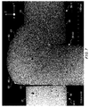
- FIG. 7 is a cross sectional photograph of the connection terminal 20 -A 1 , the bus bar 30 - 1 , and the fusing portion 60 .
- the photograph shown in FIG. 7 corresponds to FIG. 6 .
- FIG. 8 is a photograph of the connection terminal 20 -A 1 , the bus bar 30 - 1 , and the fusing portion 60 taken from above.
- FIG. 8 is also a photograph of the fusing portion 60 before being cut off, taken from above.
- FIG. 8 is a photograph of the connection terminal 20 and the bus bar 30 which are seen from above, with addition of a center 120 , radiuses 122 , an arc 124 , and a central angle 126 of a circular shape of the connection terminal 20 , as well as a boundary (the dashed line) between the top part 21 and the taper part 26 before the welding process, and the like. Note that, in FIG. 8 , two-way arrows are illustrated for the arc 124 and the diameter respectively. In a region where the fusing portion 60 and the connection terminal 20 overlap each other, the outline of the connection terminal 20 is partially in a circular shape.
- the length of the arc 124 is defined by the center 120 and the radius 122 of the connection terminal 20 .
- the sectorial shaped central angle 126 is defined by the center 120 and the radius 122 of the circular shape of the connection terminal 20 .
- the taper part 26 of the connection terminal 20 and a center 66 of the fusing portion 60 may overlap each other.
- the center of laser light is irradiated on the taper part 26 of the connection terminal 20 .
- the fusing portion 60 is observed as a nugget. Since the outline of the fusing portion 60 corresponds to the actual spread of the fused connection terminal 20 , it may not be a perfect circle completely, and it may be in a substantially circular shape. The outline of the fusing portion 60 may be approximately in a circular shape, or may also be approximately in an ellipse shape. It is apparent from the drawing that, even if it is approximately in a circular shape, the center 66 of the fusing portion 60 is positioned in the taper part 26 . Note that, the center 66 may be the power peak position of the laser light.
- the fusing portions 60 are provided to the connection terminals 20 with a ratio of 1:1.
- One fusing portion 60 may mean that, there is one region where the welded connection terminal 20 is continuously provided to it when it is seen from above. It is advantageous that, by providing the fusing portions 60 to the connection terminals 20 with a ratio of 1:1, work time in the welding process can be reduced while intensity of the fusing portion 60 is secured.
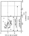
- FIG. 9 is an experimental result illustrating a relation between the clearance C between the connection terminal 20 and the bus bar 30 , and length of the arc 124 after welding.
- the horizontal axis indicates the clearance C [mm]
- the vertical axis indicates the length of the arc 124 [mm].
- the diameter ⁇ T of the connection terminal 20 was between 0.98 mm and 1.02 mm inclusive.
- a first group and a second group were prepared for the bus bar 30 .
- the first group had a diameter ⁇ B of the opening 32 , which is between 1.03 mm and 1.08 mm inclusive
- the second group had a diameter (p B of the opening 32 , which is between 1.05 mm and 1.15 mm inclusive.
- any samples of the first group had the arc 124 of 0.7 mm or longer in length.
- tensile strength can be 40 N or more.
- FIG. 10 is an experimental result illustrating relations between length of the arcs 124 and tensile strength after welding.
- the horizontal axis indicates length of the arcs 124 [mm], and the vertical axis indicates tensile strength [N] which is the same as that in FIG. 4 .
- relations between length of the arcs 124 and tensile strength were measured for 179 samples.
- ⁇ indicates standard deviation
- 36 means three times the standard deviation.
- straight lines to indicate ⁇ 3 ⁇ are illustrated with the dashed lines
- a straight line to indicate a regression line is illustrated with the dashed line between the straight lines illustrating ⁇ 3 ⁇ .
- a correlation coefficient of the regression line was 0.904.
- a length of the arc 124 may be between 0.75 mm and 2.50 mm inclusive, and more preferably, it may be between 1.03 mm and 1.57 mm inclusive.
- a length 0.75 mm of the arc 124 may be the minimal length required to achieve tensile strength of 40 N or more. For example, tensile strength that is calculated from the regression line is 40 N for the arc 124 of a length 0.75 mm. If the length of the arc 124 is longer than 2.50 mm, since the volume of the connection terminal 20 to be fused by laser light becomes comparatively large, the fused portion may pass beyond the thickness of the bus bar 30 in the Z axis direction, and may flow out from the lower surface 36 of the bus bar 30 .
- a length 1.03 mm of the arc 124 may be the minimal length required to achieve tensile strength of 40 N or more in the range of ⁇ 3 ⁇ . Also, by making the length of an arc 124 1.57 mm or shorter, tensile strength equivalent to that in a case in which a length of an arc 124 is made longer than 1.57 mm can be obtained, and of course, tensile strength of 40 N or more can be secured. In addition, by making the length of the arc 124 1.57 mm or shorter, the range of the fusing portion 60 can be made small, compared to a case in which the length of the arc 124 is made longer than 1.57 mm. Limiting the range of the fusing portion 60 is advantageous with respect to an irradiation range, amplitude of output, irradiation time, and the like of the laser light.
- FIG. 11 is a cross sectional photograph of a connection terminal 20 -A 1 , a bus bar 30 - 1 , and a fusing portion 60 in a comparative example.
- height positions of a top part 21 of the connection terminal 20 and an upper surface 34 of the bus bar 30 are made to be coincident with each other, and then laser light was irradiated on a predetermined region over the top part 21 and the upper surface 34 . It was observed that cracks had occurred directly below the fusing portion 60 .
- FIG. 12 is a drawing illustrating a cross section taken along A-A of a power semiconductor device 210 in the second embodiment.
- Connection terminals 20 of the present example do not have taper parts 26 .
- the connection terminals 20 of the present example are composed of top parts 21 and circular pillars 27 .
- the taper parts 38 may make diameters of the openings 32 to become small from the lower surfaces 36 toward upper surfaces 34 .
- the taper parts 38 are provided to reach predetermined height positions from the lower surfaces 36 in the +Z direction, and the rest of the portions are provided with cylindrical portions illustrated in the first embodiment. More specifically, the lower half and the upper half in the Z axis direction are the taper parts 38 and the cylindrical portions respectively. Note that, the present embodiment having the bus bars 30 that are provided with the taper parts 38 may be combined with the first embodiment.
- FIG. 13 is a top view of a bus bar 30 - 1 and one connection terminal 20 -A 1 after welding.
- FIG. 13 is also a drawing of the bus bar 30 - 1 that is seen from above. Note that, in FIG. 13 , right side of the bus bar 30 - 1 is omitted.
- a center 66 of a fusing portion 60 that is provided on the bus bar 30 - 1 may be provided off-centered from a center 120 of the connection terminal 20 -A 1 in a certain direction.
- the center 66 of the fusing portion 60 does not overlap with the center 120 of the connection terminal 20 , and is off-centered from the center 120 in the +Y direction.
- the connection terminal 20 is provided with hatching
- the fusing portion 60 is provided with cross-hatching.
- FIG. 14 is a top view illustrating a first modification example of the bus bar 30 - 1 and a plurality of connection terminals 20 after welding.
- a power semiconductor module 100 of the present example has connection terminals 20 . Six of which correspond to a drain terminal, a source terminal, and an output terminal respectively, instead of two of which correspond to them respectively.
- openings 32 -A 2 , 32 -A 4 , and 32 -A 6 on the bus bar 30 - 1 of the present example has which are provided to be spaced apart from the plurality of opening 32 -A 1 , 32 -A 3 , and 32 -A 5 in a long-side direction of the bus bar 30 - 1 , and to be side by side in a short side direction.
- connection terminals 20 are provided corresponding to the openings 32 of the present example.
- the short side direction is parallel with the Y axis direction
- the long-side direction is parallel with the X axis direction.
- one example of the first direction is the Y axis direction
- one example of the second direction is the X axis direction.
- a plurality of fusing portions 60 are provided on the bus bar 30 - 1 . Also, the plurality of the fusing portions 60 are provided side by side in the Y axis direction corresponding to positional relations between the connection terminals 20 and the openings 32 . In addition, each of the plurality of fusing portions 60 is provided off-centered from the center 120 of each connection terminals 20 in the same certain direction in the Y axis direction (in the present example, the +Y direction). Note that, the fusing portions 60 to be off-centered from the centers 120 of the connection terminals 20 in certain directions means, for example, the centers 66 of the fusing portions 60 are off-centered from the centers 120 of the connection terminals 20 in certain directions.
- connection terminals 20 and the openings 32 in the fusing portions 60 By providing the fusing portions 60 to be off-centered from the centers 120 to the same certain directions, resistance can be improved against torque having a direction parallel with the Z axis direction as a rotation axis. That is, even if torque of a kind to rotate the bus bar 30 - 1 in an X-Y plane is applied, physical connections become easy to be maintained between the connection terminals 20 and the openings 32 in the fusing portions 60 .
- the number (the first number) of the fusing portions 60 to be provided corresponding to the connection terminals 20 -A 1 , 20 -A 3 , and 20 -A 5 is 3.
- the number (the second number) of the fusing portions 60 to be provided corresponding to the connection terminals 20 -A 2 , 20 -A 4 , and 20 -A 6 is also 3.
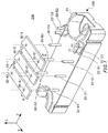
- FIG. 15 is a perspective view illustrating a part of a power semiconductor device 220 in the third embodiment.
- the power semiconductor device 220 of the present example has a power semiconductor module 110 and bus bars 70 .
- the power semiconductor module 110 has connection terminals 20 . Six of which correspond to a drain terminal, a source terminal and an output terminal respectively, instead of 2 of which correspond to them respectively. Illustrated in FIG. 15 are connection terminals 20 -A 1 to 20 -A 6 which correspond to the drain terminal, connection terminals 20 -B 1 to 20 -B 6 which correspond to the source terminal, and connection terminals 20 -C 1 to 20 -C 6 which correspond to the output terminal. Note that, the number of connection terminals 20 is not limited to 6.
- connection terminals 22 -D 1 and 22 -D 2 which are source sensing terminals, and two connection terminals 22 -E 1 and 22 -E 2 which are gate terminals are provided, similar to those in the first embodiment.
- the bus bar 70 is one plate including a convex 80 and flat parts 84 .
- the convex 80 means a portion other than the flat parts 84 that are parallel with the X-Y plane.
- the convex 80 of the present example is in a hat shape.
- the convex 80 may include a portion of the bus bar 70 which is protruding from the flat parts 84 in +Z direction.
- Convexes 80 have connection openings 79 through which fixing members 90 pass to fix bus bars 70 and external connection terminals.
- Fixing members 90 may be screws having head parts 91 that are provided with grooves or holes for turning, and stem parts 93 that are provided with grooves on their surfaces.
- Nuts 92 are members having female screws that are rotatably coupled to male screws of the stem parts 93 .
- the fixing members 90 and the nuts 92 may have functions to sandwich and fix external connection terminals and the bus bars 70 between the head parts 91 and upper surfaces of the convexes 80 .
- Diameters of the head parts 91 and the nuts 92 may be greater than diameters of connection openings 79 on the convexes 80 .
- the bus bars 70 in the present example have first flat parts 84 - 1 positioned on first sides of the convexes 80 in directions parallel with the X axis direction, and second flat parts 84 - 2 positioned on second sides to the convexes 80 in directions parallel with the X axis direction.
- the first flat parts 84 - 1 and the second flat parts 84 - 2 in the present example sandwich the convexes 80 in the X axis direction.
- the external connection terminals have been omitted from FIG. 15 .
- the present example is different from the first embodiment mainly on this point described above, and all other components may be the same as the first embodiment. Thus, the same advantageous effect is obtained for the same technical feature as that of the first embodiment.
- FIG. 16A is a top view of a bus bar 70 - 1 and the connection terminals 20 -A 1 to 20 -A 6 before welding. Illustrated in FIG. 16A is a state in which the connection terminals 20 -A 1 to 20 -A 6 have been made to pass through openings 72 -A 1 to 72 -A 6 respectively, and before welding each connection terminals 20 by laser light. If the bus bar 70 is seen from above, the bus bar 70 may be in a rectangular shape.
- the bus bar 70 in the present example has short sides 83 parallel with the Y axis direction and long sides 85 parallel with the X axis direction.
- FIG. 16B is a top view of the bus bar 70 - 1 and connection terminals 20 -A 1 to 20 -A 6 after welding.
- a first flat part 84 - 1 may be provided with a first number of fusing portions 60 - 1 being side by side in the direction parallel with the Y axis direction.
- the connection terminals 20 are provided with hatching, and the fusing portions 60 are provided with cross-hatching.
- a second flat part 84 - 2 may be provided with a second number of fusing portions 60 - 2 that are provided side by side in the direction parallel with the Y axis direction.
- the first number and the second number are 3, respectively.
- Each of the first number of fusing portions 60 - 1 and the second number of fusing portions 60 - 2 may be provided off-centered from the centers 120 of the connection terminals 20 to the same certain direction in the Y axis direction.
- each of the fusing portions 60 - 1 and 60 - 2 is provided off-centered from the centers 120 of the connection terminals 20 in the +Y direction.
- each of the fusing portions 60 - 1 and 60 - 2 may be provided off-centered from the centers 120 in the ⁇ Y direction.
- a connection opening 79 is a center of a rotation axis of torque T that is applied on bus bars 70 when the external connection terminal is installed on the bus bar 70 by the fixing member 90 and when it is removed.
- FIG. 17 is a drawing illustrating a cross section taken along B-B of FIG. 16A .
- the B-B cross section is a cross section parallel with an X-Z plane that passes through the connection terminals 20 -A 5 and 20 -A 6 .
- the convex 80 has two sides 81 , and a top part 82 sandwiched by the two sides.
- a side 81 - 1 in the present example has one side that is connected to the top part 82 and the other side that is connected to the first flat part 84 - 1 .
- a side 81 - 2 in the present example has one side that is connected to the top part 82 and the other side that is connected to a second flat part 84 - 2 .
- the bus bar 70 of the present example has body parts 73 , and third plated layers 75 provided on surfaces of the body parts 73 .
- upper surfaces 74 are surfaces of the bus bar 70 in the +Z direction
- lower surfaces 76 are surfaces in the ⁇ Z direction.
- the +Z direction surfaces and the ⁇ Z direction surfaces of the first flat part 84 - 1 , the sides 81 - 1 and 81 - 2 , the top part 82 , and the second flat part 84 - 2 are referred to as the upper surfaces 74 and the lower surfaces 76 , respectively.
- length from an upper end of the top part 82 of the convex 80 to an upper end of a top part 21 of the connection terminal 20 is Ls
- length from the upper end of the top part 21 to a lower end of a taper part 26 is Lt
- length from the upper end of the top part 21 to the upper surface 74 of the bus bar 70 is Lp.
- FIG. 18 is a drawing illustrating a cross section taken along C-C of FIG. 16B .
- FIG. 18 is a cross sectional view parallel with the Y-Z plane that passes through the connection terminals 20 and the bus bars 70 after welding.
- Length L 2 and L 3 may indicate the same parts as those described in FIG. 5 of the first embodiment.
- FIG. 19 is a top view illustrating a first modification example of the bus bar 70 - 1 and one connection terminal 20 after welding.
- FIG. 19 is also a drawing of the vicinity of a short side 83 - 1 of the flat part 84 - 1 in the bus bar 70 - 1 that is seen from above.
- the first flat part 84 - 1 is provided with one opening 72 -A 1 , and accordingly, it is provided with one connection terminal 20 -A 1 and one fusing portion 60 - 1 .
- a fusing portion 60 - 1 provided on a bus bar 70 - 1 may be provided off-centered from a center 120 of a connection terminal 20 -A 1 in a certain direction.
- connection terminal 20 is provided with hatching
- the fusing portion 60 is provided with cross-hatching. Note that, configuration of connection terminals 20 , openings 72 , and fusing portions 60 in a flat part 84 - 2 may also be the same as that in a flat part 84 - 1 .
- FIG. 20 is a drawing illustrating a cross section taken along D-D of FIG. 15 after welding.
- FIG. 20 illustrates a state in which an external connection terminal 95 and the bus bar 70 are physically contacting each other by the fixing member 90 and a nut 92 .
- the top part 82 of the convex 80 may be positioned above an upper end 62 of the connection terminal 20 .
- H B -H M is preferably 0.2 mm or longer, and more preferably, 0.5 mm or longer. Also, H M /H B is preferably 0.71 or less, and more preferably, 0.50 or less. If H B -H M and H M /H B is within the above-mentioned range, even if the bus bar 70 is pushed in the Z axis direction and distorted when installing the external connection terminal 95 , the fusing portion 60 can be prevented from receiving damage.
- a lower surface 76 of the top part 82 in the convex 80 may be positioned above the upper surfaces 74 of the flat parts 84 in the bus bar 70 other than that of the convex 80 (this situation is illustrated with H FB ).
- the top part 82 of the convex 80 of the present example is not in a so-called thick shape, where the lower surface 76 of the top part 82 is positioned below the upper surfaces 74 of the flat parts 84 . Thereby, in a screw-tightening process, the top part 82 is easy to be deformed corresponding to the torque T that is applied on the bus bar 70 from the fixing member 90 , compared to a case in which the top part 82 is in a so-called thick shape.
- the thickness of the top part 82 in the Z axis direction is the same as the thickness of the flat parts 84 in the Z axis direction, and the lower surface 76 of the top part 82 is positioned above the upper surfaces 74 of the flat parts 84 .
- the thickness of the top part 82 in the Z axis direction may be thicker than the thickness of the flat parts 84 in the Z axis direction, or it may also be thinner than that. It is advantageous that, if the top part 82 and sides 81 of the convex 80 , and the flat parts 84 have the same thickness, the bus bar 70 can be formed by deforming one plate.
- FIG. 21 is a drawing illustrating a cross section taken along D-D of FIG. 15 after welding, in a first modification example.
- the present example is an example in which height positions of the lower surface 76 of the convex 80 and the lower surfaces 76 of the flat parts 84 are coincident with each other, in the third embodiment.
- a diameter of the connection opening 79 of the present example may be larger than a diameter of the stem part 93 (that is, it may be a clearance hole), or it may be the same as the diameter of the stem part 93 .
- H M ⁇ H B increase in contact resistance can be prevented in the fusing portions 60 .
- FIG. 22 is a drawing illustrating a cross section taken along D-D of FIG. 15 after welding, in a second modification example.
- the present example is an example in which height positions of the lower surface 76 of the convex 80 and the lower surfaces 76 of the flat parts 84 are coincident with each other, in the third embodiment.
- the bus bar 70 of the present example has a concave 88 in a height range between the upper surface 74 and the lower surface 76 of the convex 80 , which is larger than the diameter of the stem part 93 of the fixing member 90 .
- a height position of an upper surface 74 of the concave 88 is coincident with a height position of an upper surface 74 of the flat part 84 .
- connection opening 79 on the bus bar 70 of the present example which is open from the upper surface 74 corresponding to the bottom of the concave 88 all the way through to the lower surface 76 , and which accommodates the stem part 93 of the fixing member 90 .
- FIG. 23 is a drawing illustrating a cross section taken along B-B of FIG. 16A in the fourth embodiment.
- the taper parts 78 may make diameters of the openings 72 to become small from the lower surfaces 76 toward the upper surfaces 74 .
- the taper parts 78 are provided from the lower surfaces 76 to reach predetermined height positions in the +Z direction, and the rest of the portions are provided with cylindrical portions that are the same as those in the third embodiment. More specifically, the lower half and the upper half in the Z axis direction are the taper parts 78 and the cylindrical portions respectively. Note that, the present embodiment having the bus bar 70 that is provided with the taper parts 78 may be combined with the third embodiment.
Landscapes
- Engineering & Computer Science (AREA)
- Power Engineering (AREA)
- Microelectronics & Electronic Packaging (AREA)
- Computer Hardware Design (AREA)
- Physics & Mathematics (AREA)
- General Physics & Mathematics (AREA)
- Condensed Matter Physics & Semiconductors (AREA)
- Manufacturing & Machinery (AREA)
- Ceramic Engineering (AREA)
- Chemical & Material Sciences (AREA)
- Optics & Photonics (AREA)
- Materials Engineering (AREA)
- Connections Effected By Soldering, Adhesion, Or Permanent Deformation (AREA)
- Laser Beam Processing (AREA)
- Connection Of Batteries Or Terminals (AREA)
Applications Claiming Priority (2)
| Application Number | Priority Date | Filing Date | Title |
|---|---|---|---|
| JP2017-166275 | 2017-08-30 | ||
| JP2017166275A JP7006024B2 (ja) | 2017-08-30 | 2017-08-30 | 半導体装置及びその製造方法 |
Publications (2)
| Publication Number | Publication Date |
|---|---|
| US20190067166A1 US20190067166A1 (en) | 2019-02-28 |
| US10629517B2 true US10629517B2 (en) | 2020-04-21 |
Family
ID=65321845
Family Applications (1)
| Application Number | Title | Priority Date | Filing Date |
|---|---|---|---|
| US16/016,682 Active US10629517B2 (en) | 2017-08-30 | 2018-06-25 | Semiconductor device and fabrication method thereof |
Country Status (4)
| Country | Link |
|---|---|
| US (1) | US10629517B2 (zh) |
| JP (1) | JP7006024B2 (zh) |
| CN (1) | CN109427721B (zh) |
| DE (1) | DE102018210867A1 (zh) |
Families Citing this family (6)
| Publication number | Priority date | Publication date | Assignee | Title |
|---|---|---|---|---|
| JP7451905B2 (ja) * | 2019-09-03 | 2024-03-19 | 富士電機株式会社 | 半導体装置及び半導体装置の製造方法 |
| CN111162443B (zh) * | 2019-12-31 | 2021-08-17 | 芯思杰技术(深圳)股份有限公司 | 焊接方法和焊接设备 |
| WO2021182643A1 (ja) | 2020-03-13 | 2021-09-16 | 古河電気工業株式会社 | 溶接方法、レーザ溶接システム、金属部材、電気部品、および電子機器 |
| CN111261317B (zh) * | 2020-04-09 | 2021-08-31 | 江东合金技术有限公司 | 一种特种电缆用高性能抗氧化铜导体材料的制备方法 |
| JP2022180181A (ja) * | 2021-05-24 | 2022-12-06 | 富士電機株式会社 | 半導体装置 |
| FR3143911A1 (fr) * | 2022-12-16 | 2024-06-21 | Valeo Eautomotive France Sas | Moyen de connexion électrique d’un module de puissance et d’une barre de connexion |
Citations (28)
| Publication number | Priority date | Publication date | Assignee | Title |
|---|---|---|---|---|
| US5272590A (en) * | 1990-02-12 | 1993-12-21 | Hernandez Jorge M | Integrated circuit package having an internal cavity for incorporating decoupling capacitor |
| US5914527A (en) * | 1998-03-13 | 1999-06-22 | Microsemi Corporation | Semiconductor device |
| US6111199A (en) * | 1998-04-07 | 2000-08-29 | Integrated Device Technology, Inc. | Integrated circuit package using a gas to insulate electrical conductors |
| US6344682B1 (en) * | 1999-02-01 | 2002-02-05 | Mitsubishi Denki Kabushiki Kaisha | Semiconductor device comprising a semiconductor element mounted on a substrate and covered by a wiring board |
| US6741778B1 (en) * | 2000-05-23 | 2004-05-25 | International Business Machines Corporation | Optical device with chip level precision alignment |
| US20080185708A1 (en) * | 2007-02-05 | 2008-08-07 | Bridge Semiconductor Corporation | Stackable semiconductor package having metal pin within through hole of package |
| US20090278246A1 (en) * | 2005-09-06 | 2009-11-12 | Nec Corporation | Semiconductor device |
| US20100013086A1 (en) * | 2008-07-18 | 2010-01-21 | Mitsubishi Electric Corporation | Power semiconductor device |
| US20110193105A1 (en) * | 2010-08-27 | 2011-08-11 | Quarkstar, Llc | Solid State Light Sheet for General Illumination Having Substrates for Creating Series Connection of Dies |
| US20120112332A1 (en) * | 2010-06-11 | 2012-05-10 | Masanori Minamio | Resin-sealed semiconductor device and method for fabricating the same |
| US20120127681A1 (en) * | 2010-11-24 | 2012-05-24 | Samsung Electro-Mechanics Co., Ltd. | Soldering connecting pin, semiconductor package substrate and method of mounting semiconductor chip using the same |
| US20120155055A1 (en) * | 2010-12-21 | 2012-06-21 | Tessera, Inc. | Semiconductor chip assembly and method for making same |
| US20120241953A1 (en) * | 2010-01-05 | 2012-09-27 | Fuji Electric Co., Ltd | Unit for semiconductor device and semiconductor device |
| US20120318346A1 (en) * | 2011-03-31 | 2012-12-20 | Sony Corporation | Method of manufacturing photoelectric conversion element, photoelectric conversion element, and electronic apparatus |
| US20140346630A1 (en) * | 2013-05-24 | 2014-11-27 | Oxford Instruments Analytical Oy | Semiconductor detector head and a method for manufacturing the same |
| US20140355219A1 (en) | 2013-06-04 | 2014-12-04 | Fuji Electric Co., Ltd. | Semiconductor device |
| US20140370663A1 (en) * | 2013-06-18 | 2014-12-18 | Infineon Technologies Ag | Method for Producing a Semiconductor Module |
| US20150223339A1 (en) * | 2012-10-15 | 2015-08-06 | Fuji Electric Co., Ltd. | Semiconductor device |
| US20150303164A1 (en) * | 2014-04-17 | 2015-10-22 | Delta Electronics Int'l (Singapore) Pte Ltd | Package structure |
| US9299637B2 (en) * | 2013-10-30 | 2016-03-29 | Fuji Electric Co., Ltd. | Semiconductor module |
| US20160240452A1 (en) * | 2015-02-18 | 2016-08-18 | Semiconductor Components Industries, Llc | Semiconductor packages with sub-terminals and related methods |
| US20160247735A1 (en) * | 2015-02-19 | 2016-08-25 | Semiconductor Components Industries, Llc | Semiconductor package with elastic coupler and related methods |
| US20170113387A1 (en) * | 2015-06-29 | 2017-04-27 | Gregory Arther Huber | Insertable aperture molding |
| US20180012833A1 (en) * | 2016-07-08 | 2018-01-11 | Kabushiki Kaisha Toyota Jidoshokki | Semiconductor module |
| US20180126175A1 (en) * | 2016-11-08 | 2018-05-10 | Greatbatch Ltd. | Hermetic terminal for an aimd having a composite brazed conductive lead |
| US10163868B2 (en) * | 2013-05-16 | 2018-12-25 | Fuji Electric Co., Ltd. | Semiconductor device |
| US20190064219A1 (en) * | 2017-08-22 | 2019-02-28 | Samsung Electronics Co., Ltd. | Probe card, test apparatus including the probe card, and related methods of manufacturing |
| US20190090393A1 (en) * | 2017-09-19 | 2019-03-21 | Panasonic Intellectual Property Management Co., Ltd. | Component mounting method and method for manufacturing component-mounted board |
Family Cites Families (4)
| Publication number | Priority date | Publication date | Assignee | Title |
|---|---|---|---|---|
| JPH05174940A (ja) * | 1991-12-18 | 1993-07-13 | Yazaki Corp | 電気接続片のレーザ溶接方法及びこの方法に使用する電気接続片 |
| JP2002025639A (ja) * | 2000-07-07 | 2002-01-25 | Sumitomo Wiring Syst Ltd | レーザ溶接接合構造 |
| JP4325550B2 (ja) * | 2004-12-20 | 2009-09-02 | トヨタ自動車株式会社 | 電子機器用バスバーと接続端子の接合構造及び接合方法 |
| JP4985012B2 (ja) * | 2007-03-22 | 2012-07-25 | 富士電機株式会社 | 半導体装置およびその製造方法 |
-
2017
- 2017-08-30 JP JP2017166275A patent/JP7006024B2/ja active Active
-
2018
- 2018-06-25 US US16/016,682 patent/US10629517B2/en active Active
- 2018-06-29 CN CN201810694822.2A patent/CN109427721B/zh active Active
- 2018-07-02 DE DE102018210867.6A patent/DE102018210867A1/de active Granted
Patent Citations (29)
| Publication number | Priority date | Publication date | Assignee | Title |
|---|---|---|---|---|
| US5272590A (en) * | 1990-02-12 | 1993-12-21 | Hernandez Jorge M | Integrated circuit package having an internal cavity for incorporating decoupling capacitor |
| US5914527A (en) * | 1998-03-13 | 1999-06-22 | Microsemi Corporation | Semiconductor device |
| US6111199A (en) * | 1998-04-07 | 2000-08-29 | Integrated Device Technology, Inc. | Integrated circuit package using a gas to insulate electrical conductors |
| US6344682B1 (en) * | 1999-02-01 | 2002-02-05 | Mitsubishi Denki Kabushiki Kaisha | Semiconductor device comprising a semiconductor element mounted on a substrate and covered by a wiring board |
| US6741778B1 (en) * | 2000-05-23 | 2004-05-25 | International Business Machines Corporation | Optical device with chip level precision alignment |
| US20090278246A1 (en) * | 2005-09-06 | 2009-11-12 | Nec Corporation | Semiconductor device |
| US20080185708A1 (en) * | 2007-02-05 | 2008-08-07 | Bridge Semiconductor Corporation | Stackable semiconductor package having metal pin within through hole of package |
| US20100013086A1 (en) * | 2008-07-18 | 2010-01-21 | Mitsubishi Electric Corporation | Power semiconductor device |
| US20120241953A1 (en) * | 2010-01-05 | 2012-09-27 | Fuji Electric Co., Ltd | Unit for semiconductor device and semiconductor device |
| US20120112332A1 (en) * | 2010-06-11 | 2012-05-10 | Masanori Minamio | Resin-sealed semiconductor device and method for fabricating the same |
| US20110193105A1 (en) * | 2010-08-27 | 2011-08-11 | Quarkstar, Llc | Solid State Light Sheet for General Illumination Having Substrates for Creating Series Connection of Dies |
| US20120127681A1 (en) * | 2010-11-24 | 2012-05-24 | Samsung Electro-Mechanics Co., Ltd. | Soldering connecting pin, semiconductor package substrate and method of mounting semiconductor chip using the same |
| US20120155055A1 (en) * | 2010-12-21 | 2012-06-21 | Tessera, Inc. | Semiconductor chip assembly and method for making same |
| US20120318346A1 (en) * | 2011-03-31 | 2012-12-20 | Sony Corporation | Method of manufacturing photoelectric conversion element, photoelectric conversion element, and electronic apparatus |
| US20150223339A1 (en) * | 2012-10-15 | 2015-08-06 | Fuji Electric Co., Ltd. | Semiconductor device |
| US10163868B2 (en) * | 2013-05-16 | 2018-12-25 | Fuji Electric Co., Ltd. | Semiconductor device |
| US20140346630A1 (en) * | 2013-05-24 | 2014-11-27 | Oxford Instruments Analytical Oy | Semiconductor detector head and a method for manufacturing the same |
| JP2014236150A (ja) | 2013-06-04 | 2014-12-15 | 富士電機株式会社 | 半導体装置 |
| US20140355219A1 (en) | 2013-06-04 | 2014-12-04 | Fuji Electric Co., Ltd. | Semiconductor device |
| US20140370663A1 (en) * | 2013-06-18 | 2014-12-18 | Infineon Technologies Ag | Method for Producing a Semiconductor Module |
| US9299637B2 (en) * | 2013-10-30 | 2016-03-29 | Fuji Electric Co., Ltd. | Semiconductor module |
| US20150303164A1 (en) * | 2014-04-17 | 2015-10-22 | Delta Electronics Int'l (Singapore) Pte Ltd | Package structure |
| US20160240452A1 (en) * | 2015-02-18 | 2016-08-18 | Semiconductor Components Industries, Llc | Semiconductor packages with sub-terminals and related methods |
| US20160247735A1 (en) * | 2015-02-19 | 2016-08-25 | Semiconductor Components Industries, Llc | Semiconductor package with elastic coupler and related methods |
| US20170113387A1 (en) * | 2015-06-29 | 2017-04-27 | Gregory Arther Huber | Insertable aperture molding |
| US20180012833A1 (en) * | 2016-07-08 | 2018-01-11 | Kabushiki Kaisha Toyota Jidoshokki | Semiconductor module |
| US20180126175A1 (en) * | 2016-11-08 | 2018-05-10 | Greatbatch Ltd. | Hermetic terminal for an aimd having a composite brazed conductive lead |
| US20190064219A1 (en) * | 2017-08-22 | 2019-02-28 | Samsung Electronics Co., Ltd. | Probe card, test apparatus including the probe card, and related methods of manufacturing |
| US20190090393A1 (en) * | 2017-09-19 | 2019-03-21 | Panasonic Intellectual Property Management Co., Ltd. | Component mounting method and method for manufacturing component-mounted board |
Also Published As
| Publication number | Publication date |
|---|---|
| JP2019046885A (ja) | 2019-03-22 |
| US20190067166A1 (en) | 2019-02-28 |
| CN109427721B (zh) | 2023-10-24 |
| JP7006024B2 (ja) | 2022-01-24 |
| CN109427721A (zh) | 2019-03-05 |
| DE102018210867A1 (de) | 2019-02-28 |
Similar Documents
| Publication | Publication Date | Title |
|---|---|---|
| US10629517B2 (en) | Semiconductor device and fabrication method thereof | |
| JP4924411B2 (ja) | 電力半導体装置 | |
| US9391006B2 (en) | Semiconductor device and method of manufacturing semiconductor device | |
| US20170103962A1 (en) | Semiconductor device and method for manufacturing same | |
| US9502327B2 (en) | Semiconductor device and method for manufacturing the same | |
| JP4885046B2 (ja) | 電力用半導体モジュール | |
| US11570921B2 (en) | Semiconductor device with stacked terminals | |
| JP2010103222A (ja) | 半導体装置 | |
| KR20180106957A (ko) | 반도체 장치와 그 제조 방법 및 전극판 | |
| CN108604579B (zh) | 电子装置及其制造方法 | |
| JP2008098586A (ja) | 半導体装置 | |
| US20140217600A1 (en) | Semiconductor device and method of manufacturing the same | |
| US20190229103A1 (en) | Semiconductor device | |
| JP4557804B2 (ja) | 半導体装置及びその製造方法 | |
| JP2019083294A (ja) | 半導体装置とその製造方法 | |
| JP6787118B2 (ja) | 半導体装置、電力変換装置、リードフレーム、および半導体装置の製造方法 | |
| KR102132056B1 (ko) | 전력 반도체 모듈 및 이의 제조 방법 | |
| JP6330640B2 (ja) | 半導体装置の製造方法 | |
| JP2001135654A (ja) | 圧接型半導体装置の製造方法 | |
| JP2014154770A (ja) | 半導体装置、及び、半導体装置の製造方法 | |
| DE112018003850B4 (de) | Halbleitereinheit und halbleitermodul | |
| EP4003632B1 (en) | Power semiconductor module and method of forming the same | |
| JP2019067950A (ja) | 半導体装置の製造方法 | |
| JP7274954B2 (ja) | 半導体装置 | |
| US11004807B2 (en) | Method of producing laminated substrate, method of producing semiconductor module, laminated substrate, and semiconductor module |
Legal Events
| Date | Code | Title | Description |
|---|---|---|---|
| AS | Assignment |
Owner name: FUJI ELECTRIC CO., LTD., JAPAN Free format text: ASSIGNMENT OF ASSIGNORS INTEREST;ASSIGNORS:SHIRATA, KENTO;ICHIKAWA, KOJI;SIGNING DATES FROM 20180430 TO 20180507;REEL/FRAME:046186/0270 |
|
| FEPP | Fee payment procedure |
Free format text: ENTITY STATUS SET TO UNDISCOUNTED (ORIGINAL EVENT CODE: BIG.); ENTITY STATUS OF PATENT OWNER: LARGE ENTITY |
|
| STPP | Information on status: patent application and granting procedure in general |
Free format text: DOCKETED NEW CASE - READY FOR EXAMINATION |
|
| STPP | Information on status: patent application and granting procedure in general |
Free format text: NON FINAL ACTION MAILED |
|
| STPP | Information on status: patent application and granting procedure in general |
Free format text: RESPONSE TO NON-FINAL OFFICE ACTION ENTERED AND FORWARDED TO EXAMINER |
|
| STPP | Information on status: patent application and granting procedure in general |
Free format text: NOTICE OF ALLOWANCE MAILED -- APPLICATION RECEIVED IN OFFICE OF PUBLICATIONS |
|
| STPP | Information on status: patent application and granting procedure in general |
Free format text: AWAITING TC RESP., ISSUE FEE NOT PAID |
|
| STCF | Information on status: patent grant |
Free format text: PATENTED CASE |
|
| MAFP | Maintenance fee payment |
Free format text: PAYMENT OF MAINTENANCE FEE, 4TH YEAR, LARGE ENTITY (ORIGINAL EVENT CODE: M1551); ENTITY STATUS OF PATENT OWNER: LARGE ENTITY Year of fee payment: 4 |