US10580715B2 - Stress buffer layer in embedded package - Google Patents
Stress buffer layer in embedded package Download PDFInfo
- Publication number
- US10580715B2 US10580715B2 US16/008,119 US201816008119A US10580715B2 US 10580715 B2 US10580715 B2 US 10580715B2 US 201816008119 A US201816008119 A US 201816008119A US 10580715 B2 US10580715 B2 US 10580715B2
- Authority
- US
- United States
- Prior art keywords
- die
- pads
- posts
- package
- conductive
- Prior art date
- Legal status (The legal status is an assumption and is not a legal conclusion. Google has not performed a legal analysis and makes no representation as to the accuracy of the status listed.)
- Active
Links
Images


Classifications
-
- H—ELECTRICITY
- H10—SEMICONDUCTOR DEVICES; ELECTRIC SOLID-STATE DEVICES NOT OTHERWISE PROVIDED FOR
- H10W—GENERIC PACKAGES, INTERCONNECTIONS, CONNECTORS OR OTHER CONSTRUCTIONAL DETAILS OF DEVICES COVERED BY CLASS H10
- H10W40/00—Arrangements for thermal protection or thermal control
- H10W40/20—Arrangements for cooling
- H10W40/22—Arrangements for cooling characterised by their shape, e.g. having conical or cylindrical projections
-
- H01L23/3675—
-
- H—ELECTRICITY
- H10—SEMICONDUCTOR DEVICES; ELECTRIC SOLID-STATE DEVICES NOT OTHERWISE PROVIDED FOR
- H10W—GENERIC PACKAGES, INTERCONNECTIONS, CONNECTORS OR OTHER CONSTRUCTIONAL DETAILS OF DEVICES COVERED BY CLASS H10
- H10W40/00—Arrangements for thermal protection or thermal control
- H10W40/20—Arrangements for cooling
- H10W40/22—Arrangements for cooling characterised by their shape, e.g. having conical or cylindrical projections
- H10W40/226—Arrangements for cooling characterised by their shape, e.g. having conical or cylindrical projections characterised by projecting parts, e.g. fins to increase surface area
- H10W40/228—Arrangements for cooling characterised by their shape, e.g. having conical or cylindrical projections characterised by projecting parts, e.g. fins to increase surface area the projecting parts being wire-shaped or pin-shaped
-
- H01L21/56—
-
- H01L24/25—
-
- H—ELECTRICITY
- H10—SEMICONDUCTOR DEVICES; ELECTRIC SOLID-STATE DEVICES NOT OTHERWISE PROVIDED FOR
- H10W—GENERIC PACKAGES, INTERCONNECTIONS, CONNECTORS OR OTHER CONSTRUCTIONAL DETAILS OF DEVICES COVERED BY CLASS H10
- H10W42/00—Arrangements for protection of devices
- H10W42/121—Arrangements for protection of devices protecting against mechanical damage
-
- H—ELECTRICITY
- H10—SEMICONDUCTOR DEVICES; ELECTRIC SOLID-STATE DEVICES NOT OTHERWISE PROVIDED FOR
- H10W—GENERIC PACKAGES, INTERCONNECTIONS, CONNECTORS OR OTHER CONSTRUCTIONAL DETAILS OF DEVICES COVERED BY CLASS H10
- H10W70/00—Package substrates; Interposers; Redistribution layers [RDL]
- H10W70/01—Manufacture or treatment
- H10W70/02—Manufacture or treatment of conductive package substrates serving as an interconnection, e.g. of metal plates
-
- H—ELECTRICITY
- H10—SEMICONDUCTOR DEVICES; ELECTRIC SOLID-STATE DEVICES NOT OTHERWISE PROVIDED FOR
- H10W—GENERIC PACKAGES, INTERCONNECTIONS, CONNECTORS OR OTHER CONSTRUCTIONAL DETAILS OF DEVICES COVERED BY CLASS H10
- H10W74/00—Encapsulations, e.g. protective coatings
- H10W74/01—Manufacture or treatment
-
- H—ELECTRICITY
- H10—SEMICONDUCTOR DEVICES; ELECTRIC SOLID-STATE DEVICES NOT OTHERWISE PROVIDED FOR
- H10W—GENERIC PACKAGES, INTERCONNECTIONS, CONNECTORS OR OTHER CONSTRUCTIONAL DETAILS OF DEVICES COVERED BY CLASS H10
- H10W74/00—Encapsulations, e.g. protective coatings
- H10W74/10—Encapsulations, e.g. protective coatings characterised by their shape or disposition
- H10W74/111—Encapsulations, e.g. protective coatings characterised by their shape or disposition the semiconductor body being completely enclosed
- H10W74/114—Encapsulations, e.g. protective coatings characterised by their shape or disposition the semiconductor body being completely enclosed by a substrate and the encapsulations
-
- H01L2224/24137—
-
- H01L2224/2518—
-
- H01L23/3736—
-
- H—ELECTRICITY
- H10—SEMICONDUCTOR DEVICES; ELECTRIC SOLID-STATE DEVICES NOT OTHERWISE PROVIDED FOR
- H10W—GENERIC PACKAGES, INTERCONNECTIONS, CONNECTORS OR OTHER CONSTRUCTIONAL DETAILS OF DEVICES COVERED BY CLASS H10
- H10W40/00—Arrangements for thermal protection or thermal control
- H10W40/20—Arrangements for cooling
- H10W40/25—Arrangements for cooling characterised by their materials
- H10W40/258—Metallic materials
-
- H—ELECTRICITY
- H10—SEMICONDUCTOR DEVICES; ELECTRIC SOLID-STATE DEVICES NOT OTHERWISE PROVIDED FOR
- H10W—GENERIC PACKAGES, INTERCONNECTIONS, CONNECTORS OR OTHER CONSTRUCTIONAL DETAILS OF DEVICES COVERED BY CLASS H10
- H10W70/00—Package substrates; Interposers; Redistribution layers [RDL]
- H10W70/60—Insulating or insulated package substrates; Interposers; Redistribution layers
- H10W70/611—Insulating or insulated package substrates; Interposers; Redistribution layers for connecting multiple chips together
- H10W70/614—Insulating or insulated package substrates; Interposers; Redistribution layers for connecting multiple chips together the multiple chips being integrally enclosed
-
- H—ELECTRICITY
- H10—SEMICONDUCTOR DEVICES; ELECTRIC SOLID-STATE DEVICES NOT OTHERWISE PROVIDED FOR
- H10W—GENERIC PACKAGES, INTERCONNECTIONS, CONNECTORS OR OTHER CONSTRUCTIONAL DETAILS OF DEVICES COVERED BY CLASS H10
- H10W90/00—Package configurations
- H10W90/10—Configurations of laterally-adjacent chips
Definitions
- the present disclosure relates to embedded packages and their manufacturing techniques, and more particularly relates to the addition of a stress buffer layer in embedded packages and related methods for manufacturing such a stress buffer layer.
- Integrated circuit (IC) dies are encapsulated in protective packages to allow easy handling and assembly onto printed circuit boards (PCBs) and to protect the dies or related components and devices from damage.
- a dielectric material such as a hard plastic, is typically used to encapsulate the dies and related components to form the package.
- the technique for physically (and thus thermo-conductively) connecting the heat spreader to the encapsulated die(s) and other components is crucial in ensuring proper heat dissipation. Cracks or other physical failures between the underlying dies and the heat spreader can result in insufficient heat dissipation, which may result in die overheating and in turn, die failure. This is usually caused due to a mismatch in the coefficient of thermal expansion (CTE) of the silicon typically used to form the underlying dies (a CTE of 3 ppm/K) and of copper typically used to form the heat spreader (a CTE of 16 ppm/K).
- CTE coefficient of thermal expansion
- FIG. 1 illustrated is a cross-sectional view of a block diagram of a conventional IC package 100 providing a direct connection between a die and a heat spreader.
- the package 100 is comprised of a circuit layer 105 and a redistribution layer (RDL) 110 .
- the circuit layer 105 includes the IC dies 115 , as well as other components such as a drive IC 120 .
- the RDL 110 typically includes a number of conductive vias 122 , such as metal pillars, and interconnects 124 , such as a metal leadframe, to provide electrical connection to electrically conductive bond pads on the die 115 and other components to other underlying circuitry.
- conductive vias 122 such as metal pillars
- interconnects 124 such as a metal leadframe
- the package 100 also includes a heat spreader 125 , which is typically composed of copper due to its excellent thermal-conductivity.
- a heat spreader 125 which is typically composed of copper due to its excellent thermal-conductivity.
- an interface 130 provided by the direct physical connection between the two exists.
- a plain metal layer which is typically also copper, may be provided as the direct interface 130 of the die 115 and the heat spreader 125 .
- CTE long term
- embedded packages are typically heated to a temperature above the solder melting temperature, typically during an infrared (IR) reflow process, to remove moisture the plastic encapsulant may have absorbed during the manufacturing process.
- IR infrared
- the CTE mismatch between the heat spreader 125 and the top surface of the die 115 can result in such cracking, with this loss in structural integrity often significantly affecting the heat dissipation capabilities of the heat spreader.
- Such cracking may also occur in response to the high temperatures experienced in extreme operating conditions for the package 100 .
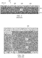
- FIG. 2 illustrated is an image from a scanning electron microscope (SEM) of a used conventional package 200 employing a direct physical connection between an encapsulated die and a heat spreader.
- the package 200 in FIG. 2 also includes a circuit layer 205 as well as an RDL 210 .
- An IC die 215 can be seen encapsulated within a dielectric material in the circuit layer 205 .
- the scan also shows a copper heat spreader 225 directly connected to the top of the die 215 for heat dissipation. Over time, a large crack 230 can be seen formed at the interface between the die 215 and the heat spreader 225 caused by the mismatch in thermal expansion between these two components of the package 200 .
- FIG. 1 scanning electron microscope
- FIG. 2A provides a close up view of a portion of the package 200 in FIG. 2 .
- the crack 230 proximate to the interface between the die 215 and the heat spreader 225 can be easily be seen. Consequently, the ability of the heat spreader 225 of this conventional package 200 to dissipate heat from the die 215 has been compromised.
- FIG. 3 illustrated is a cross-sectional view of a block diagram of another conventional IC package 300 providing an indirect connection between a die and a heat spreader.
- This conventional package 300 again includes a circuit layer 305 and an RDL 310 .
- the circuit layer 305 includes an IC die 315 in need of heat dissipation using a heat spreader 325 .
- thermally conductive vias 335 are used to provide a physical, and thus thermal, connection between the die 315 and the heat spreader 325 .
- the vias 335 are also typically formed of copper along with the heat spreader 325 , again due to copper's good thermal conductivity.
- a thin conductive seed layer 340 may also be formed on top of the die 315 to assist with thermal conductance across the top of the die 315 , as well as provide contact with the bottoms of the conductive vias 335 .
- this second conventional approach also suffers from structural disadvantages.
- the conductive vias 335 and the seed layer 340 are both typically formed of copper, the interfaces where the vias 335 contact the seed layer 340 still suffer from mechanical failure.
- the interface between the bottoms of each conductive via 335 and the top of the die 315 typically suffer structural failure, again usually in the form of cracks, not due necessarily to CTE mismatch, but instead due to high thermo-mechanical stress resulting from the relatively small diameter for each of the bottoms of the conductive vias 335 even though connected to the similar composition seed layer 340 .
- FIG. 3A provided is an SEM image 350 of a used conventional package employing conductive vias between an encapsulated die and a heat spreader.
- the image 350 shows this embodiment of a conventional package also includes a circuit layer 355 and RDL 360 , with a silicon IC die 365 encapsulated in the circuit layer 355 .
- the heat spreader 375 can be seen located above and spaced from the die 365 , with copper vias 385 providing physical, and thus thermal, connections between the die 365 and the heat spreader 375 .
- a thin conductive seed layer 390 can also be seen deposited over the top of the die 365 to assist with heat dissipation, with the copper vias 385 being physically connected to the top of the seed layer 390 at interfaces 380 .
- vias 385 by drilling down through the encapsulation material to reach the top of the die 365 or the top of the seed layer 390 .
- Typical metal deposition techniques may then be used to fill the drilled holes with copper to form the vias 385 .
- copper deposition may again be used to form the heat spreader 325 on top of the encapsulation material, and in contact with the tops of the copper vias 385 .
- the laser drilling process create via openings that are tapered from their tops to their bottoms.
- the filled conductive vias 385 have a corresponding downward, cylindrical tapering.
- This tapering of the vias 385 results in a via structure with a narrow diameter at the interface 380 with the die 365 or seed layer 390 .
- These conventional tapered via 385 structures result in less overall copper surface area conducting heat from the seed layer 390 or die 365 , which results is less heat dissipation.
- this relatively narrow interface 380 results in a high thermo-mechanical stress at the interface 380 of each via 385 , for example, after the package undergoes a reflow process.
- the high thermo-mechanical stress at the interfaces 380 will result in cracks being formed their interfaces 380 of the bottom of each via 385 , especially in extreme operating conditions for the package 300 . Also as before, such cracks result in mechanical failure for the heat dissipation intended to be provided by the conductive vias 385 . Furthermore, the inwardly tapered structure of the bottom portions of the vias 385 provides less overall thermal conductive surface contacting the die 365 or a seed layer 390 over the top surface of the die 365
- the disclosed principles provide for the creation of a stress buffer layer between an embedded IC die and a heat spreader used to dissipate heat from non-electrically conductive surfaces of the IC die.
- the stress buffer layer is comprised of a distributed set of conductive pads and a corresponding set of conductive posts formed on the conductive pads.
- the conductive pads will typically have a substantially larger width or diameter than the conductive posts.
- the relatively large diameter of the conductive pads provides a much larger interface between the conductive pads and either the top of the embedded die directly, or a conductive seed layer if one is used, and thus reduces the thermo-mechanical stress at the interface at the die associated with a CTE mismatch found in some conventional approaches discussed above.
- the large diameter of the conductive pads eliminates the high thermo-mechanical stress present when narrow, tapered conductive vias are formed using the conventional laser drilling technique discussed above.
- a stress buffer layer for use in dissipating heat within an embedded IC package.
- a stress buffer layer as disclosed herein may comprise a plurality of conductive pads laterally distributed over an IC die encapsulated in an IC package.
- Each of the plurality of conductive pads may have a proximal end contacting a non-electrically conductive surface of the IC die, and having a distal end opposite each proximal end of each conductive pad.
- such a stress buffer layer may further comprise a plurality of conductive posts laterally distributed and formed directly on each of the plurality of conductive pads.
- Each of the plurality of conductive posts may have proximal end contacting respective distal ends of each conductive pad, and a distal end opposite each proximal end of each conductive post.
- each conductive post may have a lateral width less than a lateral width of its corresponding conductive pad.
- the structure for dissipating heat from the die may further comprise a heat spreader formed over the plurality of conductive posts. The heat spreader may have a proximal surface contacting the distal ends of the plurality of conductive posts, and a distal surface exposed from the IC package.
- a disclosed method may comprise depositing a first mask layer over an IC die, and then removing areas of the first mask layer to create first openings exposing corresponding non-electrically conductive surfaces of the IC die. The method may then include forming a conductive pad in each of the first openings over the exposed corresponding non-electrically conductive surfaces of the IC die and to a height of the first mask layer.
- An exemplary method may then include depositing a second mask layer over the conductive pads and remaining portions of the first mask layer, and then removing areas of the second mask layer to create second openings, each exposing a portion of a corresponding conductive pad.
- a conductive post may then be formed in each of the second openings directly on the exposed portion of each corresponding conductive pad.
- An exemplary method may then include removing the first and second mask layers, and depositing an encapsulating dielectric material over the IC die, conductive pads, and conductive posts to a height of the conductive posts. Then, a heat spreader maybe formed on the encapsulating dielectric material and the conductive posts, and with a distal surface of the heat spreader exposed from the encapsulating dielectric material.
- FIG. 1 illustrates a cross-sectional view of a block diagram of a conventional IC package providing a direct connection between a die and a heat spreader
- FIG. 2 illustrates an image from a scanning electron microscope of a used conventional package employing a direct physical connection between an encapsulated die and a heat spreader
- FIG. 2A provides a close up view of a portion of the conventional package in FIG. 2 ;
- FIG. 3 illustrates a cross-sectional view of a block diagram of another conventional IC package providing an indirect connection between a die and a heat spreader
- FIG. 3A provides an image from a scanning electron microscope of a used conventional package employing conductive vias between an encapsulated die and a heat spreader;
- FIG. 4 illustrates a cross-sectional view of a block diagram of an embedded IC package having a heat dissipation structure constructed in accordance with the disclosed principles
- FIG. 4A illustrates a close up cross-sectional view of the stress buffer layer discussed with respect to FIG. 4 ;
- FIG. 4B illustrates a chart providing a summary of the DOE results of the development of thermo-mechanical stress cracks at the interface with an embedded die constructed with a stress buffer layer according to the disclosed principles
- FIGS. 5A-5I illustrate cross-sectional block diagrams of an exemplary process for forming a stress buffer layer for an embedded package, in accordance with the disclosed principles
- FIG. 6 illustrates a 3D view of an embedded package having one embodiment of a stress buffer layer in accordance with the disclosed principles
- FIG. 7 provides an image from a scanning electron microscope of an embedded package employing a stress buffer layer in accordance with the disclosed principles.
- the embedded IC package 400 includes a circuit layer 405 and an RDL 410 , and may be embodied as Quad Flat No-leads (QFN), Small Outline No-Lead (SON) (e.g., very small outline no-lead (VSON) or very, very small outline no-lead (WSON) packages), Land Grid Array (LGA), or other advantageous package; however, the disclosed principles may be employed with any type of embedded package employed a heat spreader or other heat dissipation structure.
- QFN Quad Flat No-leads
- SON Small Outline No-Lead
- VSON very small outline no-lead
- WSON very small outline no-lead
- LGA Land Grid Array
- an IC die 415 is encapsulated in a dielectric material, as is a drive IC 420 .
- RDL 410 Within the RDL 410 are electrically conductive vias 411 connected to electrically conductive bond pads 412 formed on an active side of the IC die 415 .
- An electrically conductive leadframe 413 is also shown connected to the conductive vias 411 for distributing electrical signals within the RDL 410 .
- a heat spreader 425 Located above the circuit layer 405 is a heat spreader 425 , which as before may be constructed of copper. Physically, and thermally, connecting the embedded die 415 to the heat spreader 425 is a stress buffer layer 430 constructed in accordance with the disclosed principles. In particular, the design and structure of the disclosed stress buffer layer 430 reduces thermo-mechanical stress at the connection to the IC die.
- the heat dissipation structure may again include an optional seed layer 440 deposited on top of the die 415 , which again can improve heat dissipation from the die 415 .
- the unique structure of the disclosed stress buffer layer 430 comprises a combination of a thermally conductive pad 445 with a conductive post 450 .
- each conductive pad 445 is in contact with non-electrically conductive surface(s) of the die 415 or seed layer 440 over the non-electrically conductive surface(s), while the distal end of each conductive pad 445 is directed away from the die 415 .
- non-electrically conductive surface(s) may include any surface of the die 415 not having electrically conductive bond pads used to electrically communicate to or from circuitry within the die 415 .
- Each conductive post 450 has its proximal end in contact with the distal end of each corresponding conductive pad 445 , while the distal end of each conductive post 450 is directed away from the conductive pads 445 .
- each conductive post 450 is in contact with the heat spreader 425 , or an optional seed layer (see FIG. 4A ) placed between the heat spreader 425 and each conductive post 450 .
- the heat spreader 425 then includes a distal surface exposed from the IC package 400 .
- both the pads 445 and posts 450 are formed of the same material to improve their bonding to one another, such as both being formed of copper due to its high thermal conductivity.
- the conductive pads 445 may have a substantially annular or substantially cylindrical shape, but other shapes for the conductive pads 445 may also be employed. As illustrated, the disclosed principles also provide that the conductive pads 445 have a substantially larger width or diameter than the conductive posts 450 .
- the relatively large diameter of the conductive pads 445 provides a much larger interface between the pads 445 and either the top, non-electrically conductive surfaces of the die 415 directly, or a conductive seed layer 440 if present, which reduces the thermo-mechanical stress at the interface at the die 415 associated with a CTE mismatch found in some conventional approaches.
- the diameters of the conductive pads 445 are not so large as to substantially equate to the contact area of a heat spreader disposed directly on the die 415 .
- the large diameter of the conductive pads 445 eliminates the high thermo-mechanical stress present when narrow, tapered conductive vias are formed using the conventional laser drilling technique discussed above.
- FIG. 4A illustrated is a close up cross-sectional view of the stress buffer layer 430 discussed with respect to FIG. 4 .
- This close up view more precisely illustrates the shape and proportion of the conductive pads 445 and the conductive posts 450 creating the stress buffer layer 430 .
- an optional seed layer 425 a may also be deposited prior to the heat spreader 425 , if desired, with the tops of the conductive posts 450 connected to the seed layer 425 a.
- the disclosed principles provide for the creation of a stress buffer layer 430 created by a plating process for forming the conductive pads 445 and the conductive posts 450 .
- the conductive pads 445 having a larger diameter than the conductive posts 450 makes a direct contact to the die 415 (or seed layer 440 ), and the larger diameter of the pads 445 results in stress distribution per unit area on a die 415 that is substantially smaller than the conventional laser drilled vias discuss above.
- the extra volume of copper (or other desirable conductive material) from larger diameter of the conductive pads 445 also improves thermal performance of a package 400 having a stress buffer layer 430 as disclosed herein.
- the design parameters associated with a stress buffer layer 430 as disclosed herein may also be adjusted based on desired thermo-mechanical stress and thermal conductivity performance of the package 400 .
- Dimension (a) is the amount of pull-back from the edge of the die 415 to the outer diameter of an outer conductive pad 445 .
- Dimension (b) is the additional radius from the conductive posts 450 provided by the larger conductive pads 445 .
- Dimension (c) is spacing between the conductive posts 450 .
- Dimension (d) is the diameter of the conductive posts 450 .
- Dimension (e) is the thickness of the heat spreader 425 .
- Dimension (f) is the total height of the conductive pads 445 and the conductive posts 450 .
- the height of the conductive posts (f) can be selected so as to move the high stress point from the die to a stress buffer layer as disclosed herein. Also, the post diameter (d) combined with the additional lateral radii provided by the larger conductive pad helps to distribute stress to a wider area on the die as compared to narrower conductive vias provide by conventional structures.
- FIG. 4B illustrates a chart providing a summary of the design of experiments (DOE) results of the development of thermo-mechanical stress cracks at the interface with an embedded die constructed with a stress buffer layer according to the disclosed principles. More specifically, the DOE results looked at a comparison of the thickness of the heat spreader (e) and the overall height of the conductive posts 450 and conductive pads 445 provided by the disclosed principles. The results demonstrate the trade-off between the thickness of the heat spreader 425 and the total height of the disclosed stress buffer layer 430 . For example, the DOE results demonstrated that minimum height of 30 ⁇ m for stress buffer layer 430 resulted in no cracks at the die interface for a heat spreader 425 thickness up to about 60 ⁇ m.
- DOE design of experiments
- FIGS. 5A-5I illustrated are cross-sectional block diagrams of an exemplary process for forming a stress buffer layer for an embedded package 500 , in accordance with the disclosed principles.
- FIG. 5A illustrates the circuit layer of an exemplary package at an intermediate stage of formation.
- the intermediate structure includes an embedded IC die 505 encapsulated with a dielectric package material 510 .
- the disclosed process deposits a first mask layer 515 .
- the first mask layer 515 may be a photolithographic mask deposited using conventional photolithographic process; however, other masking technologies, either now existing or later developed, may also be employed.
- a seed layer may also be deposited over the top of the die 505 prior to depositing the first mask layer 515 .
- FIG. 5B illustrates a cross-sectional view of the intermediate package structure at a later stage of the disclosed manufacturing process of a stress buffer layer.
- the first mask layer 515 is removed at multiple areas to create first openings 520 exposing non-electrically conductive surfaces of the embedded die 505 .
- photolithography processes may again be used to open select portions of the first mask layer 515 .
- the opened areas of the first mask layer 515 which in advantageous embodiments are substantially circular in shape, provide the locations of the conductive pads for the disclosed stress buffer layer.
- the thickness of the first mask layer 515 is used to set the thickness of the conductive pads in this embodiment.
- FIG. 5C illustrates a cross-sectional view of the intermediate package structure at a further stage of the disclosed manufacturing process of a stress buffer layer.
- the conductive pads 525 are formed directly on top of corresponding non-electrically conductive surfaces of the die 505 .
- the conductive pads 525 are formed on the seed layer.
- the disclosed principles may employ a plating process, such as a copper plating process.
- the conductive pads 525 may be formed using a deposition technique used in semiconductor manufacturing, or any other advantageous process for metal deposition or formation.
- FIG. 5D illustrates a cross-sectional view of the intermediate package structure at an even later stage of the disclosed manufacturing process.
- a second mask layer 530 is formed over the finished conductive pads 525 , as well as the remaining portions of the first mask layer 515 .
- the second mask layer 530 may again be formed using photolithographic processes, or any other advantageous process.
- the second mask layer 530 may be formed using the same process as the first mask layer 515 , but no such limitation is required.
- the second mask layer 530 may be comprised of a different material than the first mask layer 515 , and thus be deposited or otherwise formed using a different process.
- FIG. 5E illustrates a cross-sectional view of the intermediate package structure at a further stage of the disclosed manufacturing process of a stress buffer layer.
- the second mask layer 530 is removed at multiple areas to create second openings 535 exposing portions of the previously formed conductive pads 525 .
- photolithography processes may again be used to open select portions of the second mask layer 530 .
- the openings 535 of the second mask layer 530 which may again also be substantially circular in shape, provide the precise locations and shapes of the conductive posts 540 with respect to the conductive pads 525 , and thus may be centered over the conductive pads 525 .
- FIG. 5F illustrates a cross-sectional view of the intermediate package structure at a further stage of the disclosed manufacturing process of a stress buffer layer.
- the conductive posts 540 are created within the second openings 535 in the second mask layer 530 .
- the posts 540 may be created using a plating process, such as a copper plating process.
- the posts 540 may be formed using a deposition technique used in semiconductor manufacturing or another advantageous process for metal deposition or formation.
- the height of the posts 540 is determined by the thickness of the second mask layer 530 .
- the posts 540 may also be formed in a cylindrical shape; however, other shapes for the posts 540 may also be used.
- FIG. 5G illustrates a cross-sectional view of the intermediate package structure at a further stage of the disclosed manufacturing process of a stress buffer layer.
- the first and second masks 515 , 530 are then stripped or otherwise removed from the structure. Conventional techniques for removing the masks 515 , 530 may be employed.
- FIG. 5H illustrates a cross-sectional view of the intermediate package structure further in the process. Specifically, this stage comprises the deposition of the encapsulating dielectric material 550 used to embed the die 505 and other components in the circuit layer of the package 500 . Any technique for providing the dielectric material 550 may be employed, either now existing or later developed.
- FIG. 5I illustrates a cross-sectional view of the package 500 after the disclosed manufacturing process is completed.
- the heat spreader 555 is formed on top of the dielectric material 550 .
- a plating process or other material deposition process may be employed.
- the heat spreader 555 is either placed in direct contact with the tops of the components of the stress buffer layer 545 , or alternatively a conductive seed layer 560 may first be deposited over the dielectric material 550 and in contact with the tops of the stress buffer layer 545 , and then the heat spreader 555 formed directly on top of the seed layer 560 .
- the heat spreader 555 is formed of copper; however, other metallic or conductive material may also be employed, if desired.
- the seed layer 560 if present, may also be formed from the same material as the heat spreader 555 , or another advantageous material may be employed.
- FIG. 6 illustrated is a 3D view of an embedded package 600 having one embodiment of a stress buffer layer in accordance with the disclosed principles.
- the package 600 again includes an RDL 605 and an encapsulated IC die 610 in a circuit layer of the package 600 .
- a stress buffer layer manufactured as disclosed herein to thermally connect the die 610 with a heat spreader 615 .
- the stress buffer layer is formed by pairs of conductive pads 620 and corresponding conductive posts 625 , which in this exemplary embodiment are substantially equally spaced above the upper non-electrically conductive surfaces of the die 610 . However, other spacing arrangements or layouts for the pairs of conductive pads 620 and conductive posts 625 may also be employed.
- the stress buffer layer is comprised conductive pads 620 formed directly on the top surface of the die 610 , such that proximal ends of the conductive pads 620 are in contact with the die 610 .
- an optional seed layer may also be used between the pads 620 and the die 610 .
- the conductive pads 620 are formed of copper and into a substantially cylindrical shape to a predetermined diameter (d 1 ) and to a predetermined height (h 1 ).
- Formed on top of each conductive pad 620 is a conductive post 625 , such that the proximal ends of the conductive posts 625 contact the distal ends of the conductive pads 620 .
- the conductive posts 625 are also formed of copper and have a substantially cylindrical shape.
- the conductive posts 625 are formed to a predetermined diameter (d 2 ) and to a predetermined height (h 2 ). Once each pair of the conductive posts 625 are formed on corresponding conductive pads 620 , the overall height (f) of the stress buffer layer is established. Additionally, the spacing (c) of the conductive posts 625 may also be predetermined for the stress buffer layer. In an exemplary embodiment, the overall height (f) of the stress buffer layer may be in the range of 30 ⁇ m-60 ⁇ m, with the height (h 1 ) of the conductive pads 620 in the range of about 5 ⁇ m-20 ⁇ m and the height (h 2 ) of the conductive posts 625 in the range of about 10 ⁇ m-50 ⁇ m.
- the heat spreader 615 may have a height (e) in the range of 15 ⁇ m-60 ⁇ m.
- the overall height (f) of the stress buffer layer may be about 40 ⁇ m, and the height (e) of the heat spreader 615 may also be about 40 ⁇ m.
- the height (h 1 ) of the conductive pads 620 may be about 10 ⁇ m with the height (h 2 ) of the conductive posts 625 about 30 ⁇ m.
- the ratio for the height (h 1 ) of the pads 620 as compared to the height (h 2 ) of the conductive posts 625 may be about 3:1; however, other height ratios for these two components may also be used.
- FIG. 7 provided is an image from a scanning electron microscope of a portion of an embedded package 700 employing a stress buffer layer in accordance with the disclosed principles.
- the package 700 includes a circuit layer 705 and an RDL 710 , with an embedded IC die 715 encapsulated in the circuit layer 705 .
- a stress buffer layer as disclosed herein providing a thermal connection between the top non-electrically conductive surface of the die 715 and a heat spreader 720 .
- the heat spreader 720 also has its distal surface exposed from the package 700 .
- the stress buffer layer is shown as again comprising pads 725 formed on the die 715 , and conductive posts 730 formed on top of the pads 725 .
- both the pads 725 and posts 730 may again be formed having cylindrical shapes, but other shapes may also be formed for either or both of these components of the stress buffer layer.
- the image in FIG. 7 was taken after the package 700 had gone through IR reflow, in the manner discussed above.
- the interface 735 of the pads 725 and the non-electrically conductive surface of the die 715 does not have any cracks visible in the SEM image. Consequently, the thermal conductivity of the stress buffer layer can sufficiently dissipate heat from the die 715 due to its maintained structural integrity despite the package 700 having gone through the IR reflow process.
Landscapes
- Cooling Or The Like Of Semiconductors Or Solid State Devices (AREA)
Priority Applications (6)
| Application Number | Priority Date | Filing Date | Title |
|---|---|---|---|
| US16/008,119 US10580715B2 (en) | 2018-06-14 | 2018-06-14 | Stress buffer layer in embedded package |
| PCT/US2019/037149 WO2019241610A1 (en) | 2018-06-14 | 2019-06-14 | Stress buffer layer in embedded package |
| JP2020569781A JP7563986B2 (ja) | 2018-06-14 | 2019-06-14 | 埋め込みパッケージにおける応力緩衝層 |
| CN201980030258.7A CN112074934B (zh) | 2018-06-14 | 2019-06-14 | 嵌入式封装中的应力缓冲层 |
| EP19818882.3A EP3807923A4 (en) | 2018-06-14 | 2019-06-14 | VOLTAGE BUFFER LAYER IN AN EMBEDDED PACKAGE |
| US16/808,018 US11183441B2 (en) | 2018-06-14 | 2020-03-03 | Stress buffer layer in embedded package |
Applications Claiming Priority (1)
| Application Number | Priority Date | Filing Date | Title |
|---|---|---|---|
| US16/008,119 US10580715B2 (en) | 2018-06-14 | 2018-06-14 | Stress buffer layer in embedded package |
Related Child Applications (1)
| Application Number | Title | Priority Date | Filing Date |
|---|---|---|---|
| US16/808,018 Continuation US11183441B2 (en) | 2018-06-14 | 2020-03-03 | Stress buffer layer in embedded package |
Publications (2)
| Publication Number | Publication Date |
|---|---|
| US20190385924A1 US20190385924A1 (en) | 2019-12-19 |
| US10580715B2 true US10580715B2 (en) | 2020-03-03 |
Family
ID=68840287
Family Applications (2)
| Application Number | Title | Priority Date | Filing Date |
|---|---|---|---|
| US16/008,119 Active US10580715B2 (en) | 2018-06-14 | 2018-06-14 | Stress buffer layer in embedded package |
| US16/808,018 Active US11183441B2 (en) | 2018-06-14 | 2020-03-03 | Stress buffer layer in embedded package |
Family Applications After (1)
| Application Number | Title | Priority Date | Filing Date |
|---|---|---|---|
| US16/808,018 Active US11183441B2 (en) | 2018-06-14 | 2020-03-03 | Stress buffer layer in embedded package |
Country Status (5)
| Country | Link |
|---|---|
| US (2) | US10580715B2 (https=) |
| EP (1) | EP3807923A4 (https=) |
| JP (1) | JP7563986B2 (https=) |
| CN (1) | CN112074934B (https=) |
| WO (1) | WO2019241610A1 (https=) |
Cited By (1)
| Publication number | Priority date | Publication date | Assignee | Title |
|---|---|---|---|---|
| US11183441B2 (en) * | 2018-06-14 | 2021-11-23 | Texas Instruments Incorporated | Stress buffer layer in embedded package |
Families Citing this family (5)
| Publication number | Priority date | Publication date | Assignee | Title |
|---|---|---|---|---|
| TWI734545B (zh) * | 2020-07-03 | 2021-07-21 | 財團法人工業技術研究院 | 半導體封裝結構 |
| CN114093840A (zh) * | 2021-10-27 | 2022-02-25 | 珠海越亚半导体股份有限公司 | 信热分离tmv封装结构及其制作方法 |
| CN114678335B (zh) * | 2022-05-27 | 2022-08-16 | 合肥矽迈微电子科技有限公司 | 一种芯片散热结构、工艺及半导体器件 |
| KR102684858B1 (ko) * | 2023-03-03 | 2024-07-17 | 제엠제코(주) | 열방출 포스트 접합 반도체 패키지 및 이의 제조방법 |
| US20250112107A1 (en) * | 2023-09-28 | 2025-04-03 | Stmicroelectronics International N.V. | Heat sink, slug, or spreader and method of manufacturing the same |
Citations (5)
| Publication number | Priority date | Publication date | Assignee | Title |
|---|---|---|---|---|
| US5724818A (en) * | 1995-07-27 | 1998-03-10 | Aisin Seiki Kabushiki Kaisha | Thermoelectric cooling module and method for manufacturing the same |
| US7299639B2 (en) * | 2004-06-22 | 2007-11-27 | Intel Corporation | Thermoelectric module |
| US20090072385A1 (en) * | 2007-09-14 | 2009-03-19 | Nextreme Thermal Solutions, Inc. | Electronic Assemblies Providing Active Side Heat Pumping and Related Methods and Structures |
| US20160084542A1 (en) * | 2011-12-01 | 2016-03-24 | Jae Choon Kim | Thermoelectric cooling packages and thermal management methods thereof |
| US9583474B2 (en) * | 2011-09-30 | 2017-02-28 | Taiwan Semiconductor Manufacturing Company, Ltd. | Package on packaging structure and methods of making same |
Family Cites Families (21)
| Publication number | Priority date | Publication date | Assignee | Title |
|---|---|---|---|---|
| JPH0766332A (ja) * | 1993-08-25 | 1995-03-10 | Seiko Epson Corp | 半導体装置 |
| JP2001217340A (ja) * | 2000-02-01 | 2001-08-10 | Nec Corp | 半導体装置及びその製造方法 |
| TW579555B (en) * | 2000-03-13 | 2004-03-11 | Ibm | Semiconductor chip package and packaging of integrated circuit chip in electronic apparatus |
| US8350384B2 (en) * | 2009-11-24 | 2013-01-08 | Stats Chippac, Ltd. | Semiconductor device and method of forming electrical interconnect with stress relief void |
| US7355289B2 (en) * | 2005-07-29 | 2008-04-08 | Freescale Semiconductor, Inc. | Packaged integrated circuit with enhanced thermal dissipation |
| US8008125B2 (en) * | 2009-03-06 | 2011-08-30 | General Electric Company | System and method for stacked die embedded chip build-up |
| US7960827B1 (en) * | 2009-04-09 | 2011-06-14 | Amkor Technology, Inc. | Thermal via heat spreader package and method |
| US8241955B2 (en) * | 2009-06-19 | 2012-08-14 | Stats Chippac Ltd. | Integrated circuit packaging system with mountable inward and outward interconnects and method of manufacture thereof |
| US20120032350A1 (en) * | 2010-08-06 | 2012-02-09 | Conexant Systems, Inc. | Systems and Methods for Heat Dissipation Using Thermal Conduits |
| KR101698932B1 (ko) * | 2010-08-17 | 2017-01-23 | 삼성전자 주식회사 | 반도체 패키지 및 그 제조방법 |
| US8916481B2 (en) * | 2011-11-02 | 2014-12-23 | Stmicroelectronics Pte Ltd. | Embedded wafer level package for 3D and package-on-package applications, and method of manufacture |
| US9299688B2 (en) * | 2013-12-10 | 2016-03-29 | Taiwan Semiconductor Manufacturing Company, Ltd. | Packaged semiconductor devices and methods of packaging semiconductor devices |
| DE102014101366B3 (de) * | 2014-02-04 | 2015-05-13 | Infineon Technologies Ag | Chip-Montage an über Chip hinausstehender Adhäsions- bzw. Dielektrikumsschicht auf Substrat |
| US10340199B2 (en) * | 2014-11-20 | 2019-07-02 | Mediatek Inc. | Packaging substrate with block-type via and semiconductor packages having the same |
| US9875988B2 (en) * | 2015-10-29 | 2018-01-23 | Semtech Corporation | Semiconductor device and method of forming DCALGA package using semiconductor die with micro pillars |
| CN107424973B (zh) * | 2016-05-23 | 2020-01-21 | 凤凰先驱股份有限公司 | 封装基板及其制法 |
| KR102448099B1 (ko) * | 2016-06-02 | 2022-09-27 | 에스케이하이닉스 주식회사 | 히트 스프레더 구조를 포함하는 반도체 패키지 |
| US10930596B2 (en) * | 2016-09-30 | 2021-02-23 | Intel Corporation | Embedded die on interposer packages |
| US9865570B1 (en) * | 2017-02-14 | 2018-01-09 | Globalfoundries Inc. | Integrated circuit package with thermally conductive pillar |
| US10510704B2 (en) * | 2018-01-30 | 2019-12-17 | Taiwan Semiconductor Manufacturing Co., Ltd. | Package structure and method of manufacturing the same |
| US10580715B2 (en) * | 2018-06-14 | 2020-03-03 | Texas Instruments Incorporated | Stress buffer layer in embedded package |
-
2018
- 2018-06-14 US US16/008,119 patent/US10580715B2/en active Active
-
2019
- 2019-06-14 JP JP2020569781A patent/JP7563986B2/ja active Active
- 2019-06-14 WO PCT/US2019/037149 patent/WO2019241610A1/en not_active Ceased
- 2019-06-14 EP EP19818882.3A patent/EP3807923A4/en active Pending
- 2019-06-14 CN CN201980030258.7A patent/CN112074934B/zh active Active
-
2020
- 2020-03-03 US US16/808,018 patent/US11183441B2/en active Active
Patent Citations (5)
| Publication number | Priority date | Publication date | Assignee | Title |
|---|---|---|---|---|
| US5724818A (en) * | 1995-07-27 | 1998-03-10 | Aisin Seiki Kabushiki Kaisha | Thermoelectric cooling module and method for manufacturing the same |
| US7299639B2 (en) * | 2004-06-22 | 2007-11-27 | Intel Corporation | Thermoelectric module |
| US20090072385A1 (en) * | 2007-09-14 | 2009-03-19 | Nextreme Thermal Solutions, Inc. | Electronic Assemblies Providing Active Side Heat Pumping and Related Methods and Structures |
| US9583474B2 (en) * | 2011-09-30 | 2017-02-28 | Taiwan Semiconductor Manufacturing Company, Ltd. | Package on packaging structure and methods of making same |
| US20160084542A1 (en) * | 2011-12-01 | 2016-03-24 | Jae Choon Kim | Thermoelectric cooling packages and thermal management methods thereof |
Cited By (1)
| Publication number | Priority date | Publication date | Assignee | Title |
|---|---|---|---|---|
| US11183441B2 (en) * | 2018-06-14 | 2021-11-23 | Texas Instruments Incorporated | Stress buffer layer in embedded package |
Also Published As
| Publication number | Publication date |
|---|---|
| EP3807923A4 (en) | 2021-08-11 |
| US20190385924A1 (en) | 2019-12-19 |
| CN112074934A (zh) | 2020-12-11 |
| EP3807923A1 (en) | 2021-04-21 |
| WO2019241610A1 (en) | 2019-12-19 |
| JP2021528845A (ja) | 2021-10-21 |
| US11183441B2 (en) | 2021-11-23 |
| US20200203249A1 (en) | 2020-06-25 |
| JP7563986B2 (ja) | 2024-10-08 |
| CN112074934B (zh) | 2025-03-07 |
Similar Documents
| Publication | Publication Date | Title |
|---|---|---|
| US11183441B2 (en) | Stress buffer layer in embedded package | |
| US6780673B2 (en) | Method of forming a semiconductor device package using a plate layer surrounding contact pads | |
| US9698072B2 (en) | Low-stress dual underfill packaging | |
| US8232626B2 (en) | Via and method of via forming and method of via filling | |
| CN109786262A (zh) | 互连芯片 | |
| TW201709455A (zh) | 具有空腔的微電子組件及製造方法 | |
| CN105225967B (zh) | 封装半导体器件的方法和封装的半导体器件 | |
| CN110047811A (zh) | 线路基板、堆叠式半导体组件及其制作方法 | |
| JP5350022B2 (ja) | 半導体装置、及び該半導体装置を備えた実装体 | |
| JP2005347313A (ja) | 半導体装置の製造方法 | |
| US9972555B2 (en) | Semiconductor device and method of manufacturing same | |
| CN100433313C (zh) | 用于半导体模块中的热耗散的方法和装置 | |
| CN220324452U (zh) | 一种半导体封装装置 | |
| CN113078148B (zh) | 半导体封装结构、方法、器件和电子产品 | |
| CN105742192B (zh) | 包括两步包封的制造电子器件的方法和相关器件 | |
| US12334361B2 (en) | Substrate structure, and fabrication and packaging methods thereof | |
| CN108682631B (zh) | 一种led发光面板及其制造方法 | |
| KR101348405B1 (ko) | 실리콘 기판을 이용한 발광다이오드 패키징 및 그 제조방법 | |
| KR100732288B1 (ko) | 반도체 소자의 제조 방법 | |
| CN101238574B (zh) | 具有用于隔离和钝化层的支撑结构的半导体器件 | |
| TWI860051B (zh) | 半導體結構及其形成方法、半導體裝置 | |
| CN116487344B (zh) | 三维封装结构及封装方法 | |
| US20240113064A1 (en) | Power leadframe package with reduced solder voids | |
| KR101019706B1 (ko) | 반도체 패키지 및 이의 제조 방법 | |
| KR20260061654A (ko) | 반도체 패키지 및 그 제조 방법 |
Legal Events
| Date | Code | Title | Description |
|---|---|---|---|
| AS | Assignment |
Owner name: TEXAS INSTRUMENTS INCORPORATED, TEXAS Free format text: ASSIGNMENT OF ASSIGNORS INTEREST;ASSIGNORS:KIM, WOOCHAN;MATSUURA, MASAMITSU;MASUMOTO, MUTSUMI;AND OTHERS;SIGNING DATES FROM 20180605 TO 20180612;REEL/FRAME:046085/0456 |
|
| FEPP | Fee payment procedure |
Free format text: ENTITY STATUS SET TO UNDISCOUNTED (ORIGINAL EVENT CODE: BIG.); ENTITY STATUS OF PATENT OWNER: LARGE ENTITY |
|
| STPP | Information on status: patent application and granting procedure in general |
Free format text: NOTICE OF ALLOWANCE MAILED -- APPLICATION RECEIVED IN OFFICE OF PUBLICATIONS |
|
| STPP | Information on status: patent application and granting procedure in general |
Free format text: PUBLICATIONS -- ISSUE FEE PAYMENT RECEIVED |
|
| STCF | Information on status: patent grant |
Free format text: PATENTED CASE |
|
| MAFP | Maintenance fee payment |
Free format text: PAYMENT OF MAINTENANCE FEE, 4TH YEAR, LARGE ENTITY (ORIGINAL EVENT CODE: M1551); ENTITY STATUS OF PATENT OWNER: LARGE ENTITY Year of fee payment: 4 |