CN114678335B - 一种芯片散热结构、工艺及半导体器件 - Google Patents
一种芯片散热结构、工艺及半导体器件 Download PDFInfo
- Publication number
- CN114678335B CN114678335B CN202210586279.0A CN202210586279A CN114678335B CN 114678335 B CN114678335 B CN 114678335B CN 202210586279 A CN202210586279 A CN 202210586279A CN 114678335 B CN114678335 B CN 114678335B
- Authority
- CN
- China
- Prior art keywords
- chip
- layer
- heat
- heat dissipation
- packaging
- Prior art date
- Legal status (The legal status is an assumption and is not a legal conclusion. Google has not performed a legal analysis and makes no representation as to the accuracy of the status listed.)
- Active
Links
- 230000017525 heat dissipation Effects 0.000 title claims abstract description 50
- 239000004065 semiconductor Substances 0.000 title claims abstract description 20
- 238000000034 method Methods 0.000 title abstract description 32
- 230000008569 process Effects 0.000 title abstract description 29
- 238000004806 packaging method and process Methods 0.000 claims abstract description 52
- 230000003139 buffering effect Effects 0.000 claims abstract description 4
- 239000000463 material Substances 0.000 claims description 15
- RYGMFSIKBFXOCR-UHFFFAOYSA-N Copper Chemical compound [Cu] RYGMFSIKBFXOCR-UHFFFAOYSA-N 0.000 claims description 14
- 229910052802 copper Inorganic materials 0.000 claims description 14
- 239000010949 copper Substances 0.000 claims description 14
- 238000009713 electroplating Methods 0.000 claims description 10
- 238000004544 sputter deposition Methods 0.000 claims description 6
- PXHVJJICTQNCMI-UHFFFAOYSA-N Nickel Chemical compound [Ni] PXHVJJICTQNCMI-UHFFFAOYSA-N 0.000 claims description 4
- 229910052715 tantalum Inorganic materials 0.000 claims description 3
- GUVRBAGPIYLISA-UHFFFAOYSA-N tantalum atom Chemical compound [Ta] GUVRBAGPIYLISA-UHFFFAOYSA-N 0.000 claims description 3
- WFKWXMTUELFFGS-UHFFFAOYSA-N tungsten Chemical compound [W] WFKWXMTUELFFGS-UHFFFAOYSA-N 0.000 claims description 3
- 229910052721 tungsten Inorganic materials 0.000 claims description 3
- 239000010937 tungsten Substances 0.000 claims description 3
- 229910052759 nickel Inorganic materials 0.000 claims description 2
- 238000010586 diagram Methods 0.000 description 24
- XUIMIQQOPSSXEZ-UHFFFAOYSA-N Silicon Chemical compound [Si] XUIMIQQOPSSXEZ-UHFFFAOYSA-N 0.000 description 18
- 229910052751 metal Inorganic materials 0.000 description 18
- 239000002184 metal Substances 0.000 description 18
- 229910052710 silicon Inorganic materials 0.000 description 18
- 239000010703 silicon Substances 0.000 description 18
- 239000003822 epoxy resin Substances 0.000 description 14
- 229920000647 polyepoxide Polymers 0.000 description 14
- 239000004033 plastic Substances 0.000 description 13
- 150000001875 compounds Chemical class 0.000 description 11
- 230000035882 stress Effects 0.000 description 11
- 238000004381 surface treatment Methods 0.000 description 11
- 238000000465 moulding Methods 0.000 description 10
- 230000008646 thermal stress Effects 0.000 description 10
- 230000000694 effects Effects 0.000 description 9
- 238000005538 encapsulation Methods 0.000 description 5
- 238000004519 manufacturing process Methods 0.000 description 5
- 239000002861 polymer material Substances 0.000 description 5
- 238000005520 cutting process Methods 0.000 description 4
- 238000002360 preparation method Methods 0.000 description 4
- 230000009471 action Effects 0.000 description 3
- 239000000853 adhesive Substances 0.000 description 3
- 230000001070 adhesive effect Effects 0.000 description 3
- 238000005553 drilling Methods 0.000 description 3
- 238000000227 grinding Methods 0.000 description 3
- 239000000872 buffer Substances 0.000 description 2
- 238000005516 engineering process Methods 0.000 description 2
- 238000005259 measurement Methods 0.000 description 2
- 239000005022 packaging material Substances 0.000 description 2
- 230000002093 peripheral effect Effects 0.000 description 2
- 239000000843 powder Substances 0.000 description 2
- 238000012545 processing Methods 0.000 description 2
- 229920005989 resin Polymers 0.000 description 2
- 239000011347 resin Substances 0.000 description 2
- KXGFMDJXCMQABM-UHFFFAOYSA-N 2-methoxy-6-methylphenol Chemical compound [CH]OC1=CC=CC([CH])=C1O KXGFMDJXCMQABM-UHFFFAOYSA-N 0.000 description 1
- 239000004593 Epoxy Substances 0.000 description 1
- 230000015572 biosynthetic process Effects 0.000 description 1
- 230000008859 change Effects 0.000 description 1
- 239000003795 chemical substances by application Substances 0.000 description 1
- 239000011248 coating agent Substances 0.000 description 1
- 238000000576 coating method Methods 0.000 description 1
- 238000000151 deposition Methods 0.000 description 1
- 230000008021 deposition Effects 0.000 description 1
- 229920006336 epoxy molding compound Polymers 0.000 description 1
- 238000001125 extrusion Methods 0.000 description 1
- 239000000945 filler Substances 0.000 description 1
- 239000003292 glue Substances 0.000 description 1
- 238000010438 heat treatment Methods 0.000 description 1
- 238000001746 injection moulding Methods 0.000 description 1
- 230000001788 irregular Effects 0.000 description 1
- 239000011159 matrix material Substances 0.000 description 1
- 238000012986 modification Methods 0.000 description 1
- 230000004048 modification Effects 0.000 description 1
- 239000005011 phenolic resin Substances 0.000 description 1
- 229920001568 phenolic resin Polymers 0.000 description 1
- 238000000206 photolithography Methods 0.000 description 1
- 230000005855 radiation Effects 0.000 description 1
- 238000011160 research Methods 0.000 description 1
- 238000009751 slip forming Methods 0.000 description 1
- 238000006467 substitution reaction Methods 0.000 description 1
- 238000012546 transfer Methods 0.000 description 1
Images


Classifications
-
- H—ELECTRICITY
- H01—ELECTRIC ELEMENTS
- H01L—SEMICONDUCTOR DEVICES NOT COVERED BY CLASS H10
- H01L23/00—Details of semiconductor or other solid state devices
- H01L23/562—Protection against mechanical damage
-
- H—ELECTRICITY
- H01—ELECTRIC ELEMENTS
- H01L—SEMICONDUCTOR DEVICES NOT COVERED BY CLASS H10
- H01L23/00—Details of semiconductor or other solid state devices
- H01L23/34—Arrangements for cooling, heating, ventilating or temperature compensation ; Temperature sensing arrangements
- H01L23/36—Selection of materials, or shaping, to facilitate cooling or heating, e.g. heatsinks
- H01L23/367—Cooling facilitated by shape of device
-
- H—ELECTRICITY
- H01—ELECTRIC ELEMENTS
- H01L—SEMICONDUCTOR DEVICES NOT COVERED BY CLASS H10
- H01L21/00—Processes or apparatus adapted for the manufacture or treatment of semiconductor or solid state devices or of parts thereof
- H01L21/02—Manufacture or treatment of semiconductor devices or of parts thereof
- H01L21/04—Manufacture or treatment of semiconductor devices or of parts thereof the devices having potential barriers, e.g. a PN junction, depletion layer or carrier concentration layer
- H01L21/48—Manufacture or treatment of parts, e.g. containers, prior to assembly of the devices, using processes not provided for in a single one of the subgroups H01L21/06 - H01L21/326
- H01L21/4814—Conductive parts
- H01L21/4871—Bases, plates or heatsinks
- H01L21/4875—Connection or disconnection of other leads to or from bases or plates
-
- H—ELECTRICITY
- H01—ELECTRIC ELEMENTS
- H01L—SEMICONDUCTOR DEVICES NOT COVERED BY CLASS H10
- H01L21/00—Processes or apparatus adapted for the manufacture or treatment of semiconductor or solid state devices or of parts thereof
- H01L21/02—Manufacture or treatment of semiconductor devices or of parts thereof
- H01L21/04—Manufacture or treatment of semiconductor devices or of parts thereof the devices having potential barriers, e.g. a PN junction, depletion layer or carrier concentration layer
- H01L21/50—Assembly of semiconductor devices using processes or apparatus not provided for in a single one of the subgroups H01L21/06 - H01L21/326, e.g. sealing of a cap to a base of a container
- H01L21/56—Encapsulations, e.g. encapsulation layers, coatings
- H01L21/565—Moulds
-
- H—ELECTRICITY
- H01—ELECTRIC ELEMENTS
- H01L—SEMICONDUCTOR DEVICES NOT COVERED BY CLASS H10
- H01L23/00—Details of semiconductor or other solid state devices
- H01L23/28—Encapsulations, e.g. encapsulating layers, coatings, e.g. for protection
- H01L23/31—Encapsulations, e.g. encapsulating layers, coatings, e.g. for protection characterised by the arrangement or shape
- H01L23/3107—Encapsulations, e.g. encapsulating layers, coatings, e.g. for protection characterised by the arrangement or shape the device being completely enclosed
-
- H—ELECTRICITY
- H01—ELECTRIC ELEMENTS
- H01L—SEMICONDUCTOR DEVICES NOT COVERED BY CLASS H10
- H01L23/00—Details of semiconductor or other solid state devices
- H01L23/34—Arrangements for cooling, heating, ventilating or temperature compensation ; Temperature sensing arrangements
- H01L23/36—Selection of materials, or shaping, to facilitate cooling or heating, e.g. heatsinks
- H01L23/367—Cooling facilitated by shape of device
- H01L23/3677—Wire-like or pin-like cooling fins or heat sinks
-
- H—ELECTRICITY
- H01—ELECTRIC ELEMENTS
- H01L—SEMICONDUCTOR DEVICES NOT COVERED BY CLASS H10
- H01L23/00—Details of semiconductor or other solid state devices
- H01L23/34—Arrangements for cooling, heating, ventilating or temperature compensation ; Temperature sensing arrangements
- H01L23/42—Fillings or auxiliary members in containers or encapsulations selected or arranged to facilitate heating or cooling
- H01L23/433—Auxiliary members in containers characterised by their shape, e.g. pistons
- H01L23/4334—Auxiliary members in encapsulations
-
- H—ELECTRICITY
- H01—ELECTRIC ELEMENTS
- H01L—SEMICONDUCTOR DEVICES NOT COVERED BY CLASS H10
- H01L24/00—Arrangements for connecting or disconnecting semiconductor or solid-state bodies; Methods or apparatus related thereto
- H01L24/01—Means for bonding being attached to, or being formed on, the surface to be connected, e.g. chip-to-package, die-attach, "first-level" interconnects; Manufacturing methods related thereto
- H01L24/10—Bump connectors ; Manufacturing methods related thereto
- H01L24/11—Manufacturing methods
-
- H—ELECTRICITY
- H01—ELECTRIC ELEMENTS
- H01L—SEMICONDUCTOR DEVICES NOT COVERED BY CLASS H10
- H01L24/00—Arrangements for connecting or disconnecting semiconductor or solid-state bodies; Methods or apparatus related thereto
- H01L24/01—Means for bonding being attached to, or being formed on, the surface to be connected, e.g. chip-to-package, die-attach, "first-level" interconnects; Manufacturing methods related thereto
- H01L24/10—Bump connectors ; Manufacturing methods related thereto
- H01L24/15—Structure, shape, material or disposition of the bump connectors after the connecting process
- H01L24/16—Structure, shape, material or disposition of the bump connectors after the connecting process of an individual bump connector
-
- H—ELECTRICITY
- H01—ELECTRIC ELEMENTS
- H01L—SEMICONDUCTOR DEVICES NOT COVERED BY CLASS H10
- H01L24/00—Arrangements for connecting or disconnecting semiconductor or solid-state bodies; Methods or apparatus related thereto
- H01L24/01—Means for bonding being attached to, or being formed on, the surface to be connected, e.g. chip-to-package, die-attach, "first-level" interconnects; Manufacturing methods related thereto
- H01L24/26—Layer connectors, e.g. plate connectors, solder or adhesive layers; Manufacturing methods related thereto
- H01L24/27—Manufacturing methods
-
- H—ELECTRICITY
- H01—ELECTRIC ELEMENTS
- H01L—SEMICONDUCTOR DEVICES NOT COVERED BY CLASS H10
- H01L24/00—Arrangements for connecting or disconnecting semiconductor or solid-state bodies; Methods or apparatus related thereto
- H01L24/01—Means for bonding being attached to, or being formed on, the surface to be connected, e.g. chip-to-package, die-attach, "first-level" interconnects; Manufacturing methods related thereto
- H01L24/26—Layer connectors, e.g. plate connectors, solder or adhesive layers; Manufacturing methods related thereto
- H01L24/28—Structure, shape, material or disposition of the layer connectors prior to the connecting process
- H01L24/29—Structure, shape, material or disposition of the layer connectors prior to the connecting process of an individual layer connector
-
- H—ELECTRICITY
- H01—ELECTRIC ELEMENTS
- H01L—SEMICONDUCTOR DEVICES NOT COVERED BY CLASS H10
- H01L24/00—Arrangements for connecting or disconnecting semiconductor or solid-state bodies; Methods or apparatus related thereto
- H01L24/01—Means for bonding being attached to, or being formed on, the surface to be connected, e.g. chip-to-package, die-attach, "first-level" interconnects; Manufacturing methods related thereto
- H01L24/26—Layer connectors, e.g. plate connectors, solder or adhesive layers; Manufacturing methods related thereto
- H01L24/31—Structure, shape, material or disposition of the layer connectors after the connecting process
- H01L24/32—Structure, shape, material or disposition of the layer connectors after the connecting process of an individual layer connector
-
- H—ELECTRICITY
- H01—ELECTRIC ELEMENTS
- H01L—SEMICONDUCTOR DEVICES NOT COVERED BY CLASS H10
- H01L24/00—Arrangements for connecting or disconnecting semiconductor or solid-state bodies; Methods or apparatus related thereto
- H01L24/73—Means for bonding being of different types provided for in two or more of groups H01L24/10, H01L24/18, H01L24/26, H01L24/34, H01L24/42, H01L24/50, H01L24/63, H01L24/71
-
- H—ELECTRICITY
- H01—ELECTRIC ELEMENTS
- H01L—SEMICONDUCTOR DEVICES NOT COVERED BY CLASS H10
- H01L2224/00—Indexing scheme for arrangements for connecting or disconnecting semiconductor or solid-state bodies and methods related thereto as covered by H01L24/00
- H01L2224/01—Means for bonding being attached to, or being formed on, the surface to be connected, e.g. chip-to-package, die-attach, "first-level" interconnects; Manufacturing methods related thereto
- H01L2224/10—Bump connectors; Manufacturing methods related thereto
- H01L2224/11—Manufacturing methods
- H01L2224/114—Manufacturing methods by blanket deposition of the material of the bump connector
- H01L2224/11444—Manufacturing methods by blanket deposition of the material of the bump connector in gaseous form
- H01L2224/1145—Physical vapour deposition [PVD], e.g. evaporation, or sputtering
-
- H—ELECTRICITY
- H01—ELECTRIC ELEMENTS
- H01L—SEMICONDUCTOR DEVICES NOT COVERED BY CLASS H10
- H01L2224/00—Indexing scheme for arrangements for connecting or disconnecting semiconductor or solid-state bodies and methods related thereto as covered by H01L24/00
- H01L2224/01—Means for bonding being attached to, or being formed on, the surface to be connected, e.g. chip-to-package, die-attach, "first-level" interconnects; Manufacturing methods related thereto
- H01L2224/10—Bump connectors; Manufacturing methods related thereto
- H01L2224/11—Manufacturing methods
- H01L2224/114—Manufacturing methods by blanket deposition of the material of the bump connector
- H01L2224/1146—Plating
- H01L2224/11462—Electroplating
-
- H—ELECTRICITY
- H01—ELECTRIC ELEMENTS
- H01L—SEMICONDUCTOR DEVICES NOT COVERED BY CLASS H10
- H01L2224/00—Indexing scheme for arrangements for connecting or disconnecting semiconductor or solid-state bodies and methods related thereto as covered by H01L24/00
- H01L2224/01—Means for bonding being attached to, or being formed on, the surface to be connected, e.g. chip-to-package, die-attach, "first-level" interconnects; Manufacturing methods related thereto
- H01L2224/10—Bump connectors; Manufacturing methods related thereto
- H01L2224/15—Structure, shape, material or disposition of the bump connectors after the connecting process
- H01L2224/16—Structure, shape, material or disposition of the bump connectors after the connecting process of an individual bump connector
- H01L2224/161—Disposition
- H01L2224/16151—Disposition the bump connector connecting between a semiconductor or solid-state body and an item not being a semiconductor or solid-state body, e.g. chip-to-substrate, chip-to-passive
- H01L2224/16221—Disposition the bump connector connecting between a semiconductor or solid-state body and an item not being a semiconductor or solid-state body, e.g. chip-to-substrate, chip-to-passive the body and the item being stacked
- H01L2224/16245—Disposition the bump connector connecting between a semiconductor or solid-state body and an item not being a semiconductor or solid-state body, e.g. chip-to-substrate, chip-to-passive the body and the item being stacked the item being metallic
-
- H—ELECTRICITY
- H01—ELECTRIC ELEMENTS
- H01L—SEMICONDUCTOR DEVICES NOT COVERED BY CLASS H10
- H01L2224/00—Indexing scheme for arrangements for connecting or disconnecting semiconductor or solid-state bodies and methods related thereto as covered by H01L24/00
- H01L2224/01—Means for bonding being attached to, or being formed on, the surface to be connected, e.g. chip-to-package, die-attach, "first-level" interconnects; Manufacturing methods related thereto
- H01L2224/26—Layer connectors, e.g. plate connectors, solder or adhesive layers; Manufacturing methods related thereto
- H01L2224/27—Manufacturing methods
- H01L2224/274—Manufacturing methods by blanket deposition of the material of the layer connector
- H01L2224/27444—Manufacturing methods by blanket deposition of the material of the layer connector in gaseous form
- H01L2224/2745—Physical vapour deposition [PVD], e.g. evaporation, or sputtering
-
- H—ELECTRICITY
- H01—ELECTRIC ELEMENTS
- H01L—SEMICONDUCTOR DEVICES NOT COVERED BY CLASS H10
- H01L2224/00—Indexing scheme for arrangements for connecting or disconnecting semiconductor or solid-state bodies and methods related thereto as covered by H01L24/00
- H01L2224/01—Means for bonding being attached to, or being formed on, the surface to be connected, e.g. chip-to-package, die-attach, "first-level" interconnects; Manufacturing methods related thereto
- H01L2224/26—Layer connectors, e.g. plate connectors, solder or adhesive layers; Manufacturing methods related thereto
- H01L2224/27—Manufacturing methods
- H01L2224/274—Manufacturing methods by blanket deposition of the material of the layer connector
- H01L2224/2746—Plating
- H01L2224/27462—Electroplating
-
- H—ELECTRICITY
- H01—ELECTRIC ELEMENTS
- H01L—SEMICONDUCTOR DEVICES NOT COVERED BY CLASS H10
- H01L2224/00—Indexing scheme for arrangements for connecting or disconnecting semiconductor or solid-state bodies and methods related thereto as covered by H01L24/00
- H01L2224/01—Means for bonding being attached to, or being formed on, the surface to be connected, e.g. chip-to-package, die-attach, "first-level" interconnects; Manufacturing methods related thereto
- H01L2224/26—Layer connectors, e.g. plate connectors, solder or adhesive layers; Manufacturing methods related thereto
- H01L2224/28—Structure, shape, material or disposition of the layer connectors prior to the connecting process
- H01L2224/29—Structure, shape, material or disposition of the layer connectors prior to the connecting process of an individual layer connector
- H01L2224/29001—Core members of the layer connector
- H01L2224/29099—Material
- H01L2224/291—Material with a principal constituent of the material being a metal or a metalloid, e.g. boron [B], silicon [Si], germanium [Ge], arsenic [As], antimony [Sb], tellurium [Te] and polonium [Po], and alloys thereof
- H01L2224/29138—Material with a principal constituent of the material being a metal or a metalloid, e.g. boron [B], silicon [Si], germanium [Ge], arsenic [As], antimony [Sb], tellurium [Te] and polonium [Po], and alloys thereof the principal constituent melting at a temperature of greater than or equal to 950°C and less than 1550°C
- H01L2224/29147—Copper [Cu] as principal constituent
-
- H—ELECTRICITY
- H01—ELECTRIC ELEMENTS
- H01L—SEMICONDUCTOR DEVICES NOT COVERED BY CLASS H10
- H01L2224/00—Indexing scheme for arrangements for connecting or disconnecting semiconductor or solid-state bodies and methods related thereto as covered by H01L24/00
- H01L2224/01—Means for bonding being attached to, or being formed on, the surface to be connected, e.g. chip-to-package, die-attach, "first-level" interconnects; Manufacturing methods related thereto
- H01L2224/26—Layer connectors, e.g. plate connectors, solder or adhesive layers; Manufacturing methods related thereto
- H01L2224/28—Structure, shape, material or disposition of the layer connectors prior to the connecting process
- H01L2224/29—Structure, shape, material or disposition of the layer connectors prior to the connecting process of an individual layer connector
- H01L2224/29001—Core members of the layer connector
- H01L2224/29099—Material
- H01L2224/291—Material with a principal constituent of the material being a metal or a metalloid, e.g. boron [B], silicon [Si], germanium [Ge], arsenic [As], antimony [Sb], tellurium [Te] and polonium [Po], and alloys thereof
- H01L2224/29138—Material with a principal constituent of the material being a metal or a metalloid, e.g. boron [B], silicon [Si], germanium [Ge], arsenic [As], antimony [Sb], tellurium [Te] and polonium [Po], and alloys thereof the principal constituent melting at a temperature of greater than or equal to 950°C and less than 1550°C
- H01L2224/29155—Nickel [Ni] as principal constituent
-
- H—ELECTRICITY
- H01—ELECTRIC ELEMENTS
- H01L—SEMICONDUCTOR DEVICES NOT COVERED BY CLASS H10
- H01L2224/00—Indexing scheme for arrangements for connecting or disconnecting semiconductor or solid-state bodies and methods related thereto as covered by H01L24/00
- H01L2224/01—Means for bonding being attached to, or being formed on, the surface to be connected, e.g. chip-to-package, die-attach, "first-level" interconnects; Manufacturing methods related thereto
- H01L2224/26—Layer connectors, e.g. plate connectors, solder or adhesive layers; Manufacturing methods related thereto
- H01L2224/28—Structure, shape, material or disposition of the layer connectors prior to the connecting process
- H01L2224/29—Structure, shape, material or disposition of the layer connectors prior to the connecting process of an individual layer connector
- H01L2224/29001—Core members of the layer connector
- H01L2224/29099—Material
- H01L2224/291—Material with a principal constituent of the material being a metal or a metalloid, e.g. boron [B], silicon [Si], germanium [Ge], arsenic [As], antimony [Sb], tellurium [Te] and polonium [Po], and alloys thereof
- H01L2224/29163—Material with a principal constituent of the material being a metal or a metalloid, e.g. boron [B], silicon [Si], germanium [Ge], arsenic [As], antimony [Sb], tellurium [Te] and polonium [Po], and alloys thereof the principal constituent melting at a temperature of greater than 1550°C
- H01L2224/29181—Tantalum [Ta] as principal constituent
-
- H—ELECTRICITY
- H01—ELECTRIC ELEMENTS
- H01L—SEMICONDUCTOR DEVICES NOT COVERED BY CLASS H10
- H01L2224/00—Indexing scheme for arrangements for connecting or disconnecting semiconductor or solid-state bodies and methods related thereto as covered by H01L24/00
- H01L2224/01—Means for bonding being attached to, or being formed on, the surface to be connected, e.g. chip-to-package, die-attach, "first-level" interconnects; Manufacturing methods related thereto
- H01L2224/26—Layer connectors, e.g. plate connectors, solder or adhesive layers; Manufacturing methods related thereto
- H01L2224/28—Structure, shape, material or disposition of the layer connectors prior to the connecting process
- H01L2224/29—Structure, shape, material or disposition of the layer connectors prior to the connecting process of an individual layer connector
- H01L2224/29001—Core members of the layer connector
- H01L2224/29099—Material
- H01L2224/291—Material with a principal constituent of the material being a metal or a metalloid, e.g. boron [B], silicon [Si], germanium [Ge], arsenic [As], antimony [Sb], tellurium [Te] and polonium [Po], and alloys thereof
- H01L2224/29163—Material with a principal constituent of the material being a metal or a metalloid, e.g. boron [B], silicon [Si], germanium [Ge], arsenic [As], antimony [Sb], tellurium [Te] and polonium [Po], and alloys thereof the principal constituent melting at a temperature of greater than 1550°C
- H01L2224/29184—Tungsten [W] as principal constituent
-
- H—ELECTRICITY
- H01—ELECTRIC ELEMENTS
- H01L—SEMICONDUCTOR DEVICES NOT COVERED BY CLASS H10
- H01L2224/00—Indexing scheme for arrangements for connecting or disconnecting semiconductor or solid-state bodies and methods related thereto as covered by H01L24/00
- H01L2224/01—Means for bonding being attached to, or being formed on, the surface to be connected, e.g. chip-to-package, die-attach, "first-level" interconnects; Manufacturing methods related thereto
- H01L2224/26—Layer connectors, e.g. plate connectors, solder or adhesive layers; Manufacturing methods related thereto
- H01L2224/31—Structure, shape, material or disposition of the layer connectors after the connecting process
- H01L2224/32—Structure, shape, material or disposition of the layer connectors after the connecting process of an individual layer connector
- H01L2224/321—Disposition
- H01L2224/32151—Disposition the layer connector connecting between a semiconductor or solid-state body and an item not being a semiconductor or solid-state body, e.g. chip-to-substrate, chip-to-passive
- H01L2224/32221—Disposition the layer connector connecting between a semiconductor or solid-state body and an item not being a semiconductor or solid-state body, e.g. chip-to-substrate, chip-to-passive the body and the item being stacked
- H01L2224/32245—Disposition the layer connector connecting between a semiconductor or solid-state body and an item not being a semiconductor or solid-state body, e.g. chip-to-substrate, chip-to-passive the body and the item being stacked the item being metallic
-
- H—ELECTRICITY
- H01—ELECTRIC ELEMENTS
- H01L—SEMICONDUCTOR DEVICES NOT COVERED BY CLASS H10
- H01L2224/00—Indexing scheme for arrangements for connecting or disconnecting semiconductor or solid-state bodies and methods related thereto as covered by H01L24/00
- H01L2224/73—Means for bonding being of different types provided for in two or more of groups H01L2224/10, H01L2224/18, H01L2224/26, H01L2224/34, H01L2224/42, H01L2224/50, H01L2224/63, H01L2224/71
- H01L2224/732—Location after the connecting process
- H01L2224/73201—Location after the connecting process on the same surface
- H01L2224/73203—Bump and layer connectors
-
- H—ELECTRICITY
- H01—ELECTRIC ELEMENTS
- H01L—SEMICONDUCTOR DEVICES NOT COVERED BY CLASS H10
- H01L2924/00—Indexing scheme for arrangements or methods for connecting or disconnecting semiconductor or solid-state bodies as covered by H01L24/00
- H01L2924/15—Details of package parts other than the semiconductor or other solid state devices to be connected
- H01L2924/161—Cap
- H01L2924/162—Disposition
- H01L2924/16235—Connecting to a semiconductor or solid-state bodies, i.e. cap-to-chip
-
- H—ELECTRICITY
- H01—ELECTRIC ELEMENTS
- H01L—SEMICONDUCTOR DEVICES NOT COVERED BY CLASS H10
- H01L2924/00—Indexing scheme for arrangements or methods for connecting or disconnecting semiconductor or solid-state bodies as covered by H01L24/00
- H01L2924/15—Details of package parts other than the semiconductor or other solid state devices to be connected
- H01L2924/161—Cap
- H01L2924/163—Connection portion, e.g. seal
- H01L2924/164—Material
- H01L2924/165—Material with a principal constituent of the material being a metal or a metalloid, e.g. boron [B], silicon [Si], germanium [Ge], arsenic [As], antimony [Sb], tellurium [Te] and polonium [Po], and alloys thereof
Landscapes
- Engineering & Computer Science (AREA)
- Computer Hardware Design (AREA)
- Microelectronics & Electronic Packaging (AREA)
- Power Engineering (AREA)
- Physics & Mathematics (AREA)
- Condensed Matter Physics & Semiconductors (AREA)
- General Physics & Mathematics (AREA)
- Manufacturing & Machinery (AREA)
- Chemical & Material Sciences (AREA)
- Materials Engineering (AREA)
- Cooling Or The Like Of Semiconductors Or Solid State Devices (AREA)
Abstract
本发明公开了一种芯片散热结构、工艺及半导体器件,涉及半导体封装技术领域,包括至少一芯片及封装层,所述封装层包封芯片,所述芯片的一侧电性连接有焊盘和输出管脚,所述输出管脚穿过所述封装层与所述芯片电性连接;所述封装层远离芯片焊盘的一侧整个表面设置有底部散热片,所述封装层的内部设置有用以对封装层内部结构产生的变温应力进行缓冲且传导内部热量的中部结构,本发明芯片硅产生的热量通过中部导热层传递给每个导热凸起,后散热片散热,散热片配合焊盘构成双面散热,散热效果好,散热片应力形变不直接挤压芯片,避免损坏,芯片两面结构较为对称,平衡高低温形成的应力作用,器件可靠性强,本发明制作成本低。
Description
技术领域
本发明属于半导体封装技术领域,尤其涉及一种散发芯片内部热量结构稳定的芯片散热结构、工艺及半导体器件。
背景技术
晶圆一般采用封装的方式进行包裹形成封装体,进而形成芯片,大功率半导体器件是其中的一种,塑封为封装中较常见的一种方式,目前比较常用的塑封材料为环氧树脂塑封料,功率半导体器件在工作的时候会产生越来越多的热量,为了保证其正常工作,需要维持芯片的结温在正常的范围以内,即需要对芯片进行散热。
芯片的散热方向为:热源即硅片向外部环境散热,此过程中包含硅片到外封装的热阻JC,芯片外封装到散热片的热阻CS,散热片到环境的热阻SA,因此从硅片到环境的总热阻称为JA,因此满足:JA=JC+CS+SA。
目前常见的半导体芯片散热方式,是在芯片的输出管脚处连接焊盘,焊盘用于散热,为了加强散热效果,会进一步形成底部散热片,构成双面散热,底部散热片的结构主要有两种:一种是底部散热片直接和芯片连接,这种连接的风险在于金属散热片的热膨胀系数和半导体芯片材料硅的热膨胀系数相差比较大,在高低温冲击下产生很大的应力导致芯片损坏,使得器件失效;第二种方式是在芯片的背面先做一层高分子材料(如环氧树脂塑封料,然后在高分子材料上制作底部散热片,也可继续在侧面形成散热片,这种结构可以避免高低温热应力对芯片的冲击,但由于高分子材料的热导率偏低,从而形成热阻,JA值较高,散热效率较低。
发明内容
为解决上述现有技术中的问题,本发明提供了一种可缓冲热应力、散热效果更好的芯片散热结构、工艺及半导体器件。
封装体制作过程中,为了满足散热需要,在芯片的背面直接形成底部散热片如图1a,图1b是在图1a的基础上在芯片的侧面形成侧面散热板,整体构成多面金属板散热,如五面金属板散热,芯片硅的热膨胀系数是2.5,测定温度条件为26.85℃,本申请中底部散热片和中部导热层、导热凸起的材料主要是金属铜,且本领域散热片也常用铜材料,铜的热膨胀系数为17.5,测定温度条件为20℃,膨胀系数是表征物体热膨胀性质的物理量,即表征物体受热时其长度、面积、体积增大程度的物理量,热膨胀系数越低,说明在受热的状况下,自身体积膨胀变化小,热膨胀系数越大,热应力越大,热应力又称变温应力,即物体单位面积上所承受的力越大,芯片硅和金属铜的热膨胀系数相差较大,散热片铜料和硅直接连接,高温时铜单位面积上承受的力较大挤压硅片,使得芯片损坏,器件失效。
如果在芯片的背面先做一层高分子材料,如环氧树脂塑封料,即本领域常见的EMC塑封料,内应力低且热导率也相应的低,然后在高分子材料上制作底部散热片,如图2a,图2b是在图2a的基础上在塑封料的侧面形成侧面散热板,整体构成多面金属板散热,如五面金属板散热,但是环氧树脂的导热系数为0.2~2.2 W/mK,铜的导热系数为429 W/mK,硅的导热系数为611 W/mK,其中“W”指热功率单位,“m”代表长度单位米,而“K”为绝对温度单位,虽然中间的环氧树脂料缓冲内应力,保护硅,但是铜的导热系数远远大于环氧树脂塑封料,故环氧树脂塑封料处的热阻很大,散热片铜难以将芯片硅的热量散发,散热效果极差。
为实现上述目的,本发明的一种芯片散热结构,包括至少一芯片及封装层,所述封装层包封所述芯片,所述芯片的一侧电性连接有焊盘和输出管脚,所述输出管脚穿过所述封装层与所述芯片电性连接,所述封装层远离芯片焊盘的一侧整个表面设置有底部散热片,所述封装层的内部设置有用以对封装层内部结构产生的变温应力进行缓冲且传导内部热量的中部结构。
进一步,所述中部结构包括中部导热层和至少一导热凸起,所述中部结构将晶片与底部散热片连接;
所述晶片将封装层分割为对称的上下两层,且上层封装层包封的多个导热凸起和下层封装层包封的晶片植球结构对称。
进一步,所述中部导热层设置在晶片背面和此背面对应的封装层的外表面,所述中部导热层的材料为金属铜、钨、镍或钽。
进一步,每个所述导热凸起设置在中部导热层远离晶片的一侧,每个所述导热凸起的形状为规则圆柱形或长方体形,且倾斜或竖直的设置在中部导热层的表面。
进一步,每个所述导热凸起远离中部导热层的一端与底部散热片连接。
进一步,所述中部导热层、导热凸起和底部散热片所形成的方式为电镀或溅射。
进一步,所述封装层的一个侧壁、两个侧壁、三个侧壁或者四个侧壁上均设置有侧壁散热片,所述侧壁散热片分别与底部散热片和中部导热层连接。
一种半导体器件,包括上述芯片散热结构。
一种芯片散热工艺,包括以下步骤:
封装步骤:采用注塑封装方式将中部结构、芯片和芯片的电性连接处焊盘和输出管脚均包封在封装层内;
表面处理步骤:在芯片远离焊盘的一侧通过表面处理形成中部导热层;
在中部导热层远离芯片的一侧通过表面处理形成至少一个导热凸起;在每个导热凸起暴露于封装层的一端再次表面处理形成底部散热片,表面处理的方式为电镀或者溅射;
每个所述导热凸起和中部导热层构成中部结构,所述中部结构将底部散热片和芯片连接起来,缓冲底部散热片的变温应力对芯片的挤压同时保证热量传导;
暴露步骤:研磨或钻孔暴露出导热凸起、芯片电性连接处焊盘和输出管脚。
进一步,还包括在所述封装层的一个侧壁、两个侧壁、三个侧壁或者四个侧壁上均设置有侧壁散热片,所述侧壁散热片与底部散热片和中部导热层连接。
有益效果:1、芯片硅产生的热量通过中部导热层传递给每个导热凸起,通过底部散热片散热,芯片前面的焊盘也可以用于散热,配合底部散热片构成双面散热,整体结构JA值较小,热传导快,散热效果好;
2、由于芯片的上下都有高分子材料做保护,且结构交相对对称,能够平衡高低温形成的应力作用,器件可靠性增加,底部散热片的热应力不直接挤压芯片,保护芯片,避免损坏;
3、本申请中部结构的制作成本低,相对于有同样功效的其他结构而言,本申请制作步骤简单,制作效率高,我司生产线工艺完全可以快速制作出,不需要额外增加其他步骤。
附图说明
图1a为现有的第一种封装体芯片散热的结构示意图;
图1b为在现有的第一种封装体芯片散热上形成侧面散热的结构示意图;
图2a为现有的第二种封装体芯片散热的结构示意图;
图2b为在现有的第二种封装体芯片散热上形成侧面散热的结构示意图;
图3为本发明一种芯片散热工艺的第一实施例的步骤示意图;
图4a为本发明一种芯片散热工艺的第一实施例的工艺流程图中的载板示意图;
图4b为工艺流程中的晶圆植球步骤示意图;
图4c为工艺流程中的晶圆放置步骤示意图;
图4d为工艺流程中的将晶圆和植球包封步骤示意图;
图4e为工艺流程中的暴露植球步骤示意图;
图4f为工艺流程中的形成焊盘和输出管脚步骤示意图;
图4g为工艺流程中的将焊盘和输出管脚包封步骤示意图;
图4h为工艺流程中的暴露焊盘和输出管脚步骤示意图;
图4i为工艺流程中的去除载板步骤示意图;
图4j为工艺流程中的形成中部导热层步骤示意图;
图4k为工艺流程中的形成导热凸起步骤示意图;
图4l为工艺流程中的包封导热凸起步骤示意图;
图4m为工艺流程中的暴露导热凸起步骤示意图;
图4n为工艺流程中的形成底部散热片步骤示意图;
图5为本发明一种芯片散热工艺的第二实施例的步骤示意图;
图6为本发明一种芯片散热结构、半导体器件的第一实施例的结构示意图;
图7为本发明一种芯片散热结构、半导体器件的第二实施例的结构示意图。
图中标记说明:芯片1、封装层2、中部导热层3、导热凸起4、底部散热片5、侧壁散热片6。
具体实施方式
为了更好地了解本发明的目的、结构及功能,下面结合附图1-7,对本发明提出的一种芯片散热结构、工艺及半导体器件,做进一步详细的描述。
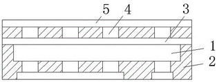
图6显示出本发明改进后的芯片散热结构、半导体器件,与现有的封装体芯片散热结构相同的是,本发明也是在封装体的外侧形成金属板用于散热,金属板通过塑封料间隔,与现有技术不同的是,本发明在塑封料间隔处设置中部结构,中部结构包括至少一个导热凸起4和中部导热层3。
至少一个导热凸起4,用于缓冲应力、传导热量和支撑结构,防止芯片损坏,散热效果佳。
此外在导热凸起4与硅之间设置中部导热层3,既可保证热量传递,又可方便导热凸起4的加工形成,同时厚度薄,热应力对器件影响较小,底部散热片5的热应力不直接挤压芯片,保护芯片,避免损坏。
芯片1将封装层2分割为对称的上下两层,且上层封装层包封的多个导热凸起4和下层封装层包封的芯片1电性连接处如植球结构对称,整个封装体的上下结构较为对称,结构稳定,器件的可靠性强。
本申请中部结构的制作成本很低,相对于有同样功效的其他结构而言,本申请制作步骤简单,制作效率高,我司生产线工艺完全可以快速制作出,不需要额外增加其他步骤,研究成本低,成本能够有效控制,散热和保护芯片的效果较好。
实施例1
图3为本发明一种芯片散热工艺第一实施例的步骤示意图,包括以下步骤:S1,提供一载板,在晶圆上形成电性连接处,即植球,后切割为单一芯片1,将一个或者多个芯片1放置在载板上并包封封装,后暴露出植球;S2,在塑封料上形成与植球连通的焊盘和输出管脚并再次包封封装,后暴露出焊盘和输出管脚,并移走载板;S3,在芯片背面和塑封料表面通过表面处理形成中部导热层3,如金属板;S4,在中部导热层3远离芯片1的一侧表面处理形成至少一个导热凸起4,如铜柱;S5,包封每个导热凸起4,后暴露出每个导热凸起4远离中部导热层3的一侧,此时整体为封装层2;S6,封装层2远离芯片1焊盘的一侧整个表面通过表面处理形成底部散热片5,每个导热凸起4与底部散热片5连接,若载板上放置多个芯片1,最后需要进行成品切割工序。
在封装层2的内部形成中部结构,即中部导热层3和至少一个导热凸起4,其将底部散热片5和芯片1背面连接起来,芯片硅产生的热量通过中部导热层3传递给每个导热凸起4,通过底部散热片5散热,热传导快,散热效果好,芯片两面结构较为对称,能够平衡高低温形成的应力作用,器件可靠性增加,芯片前面的焊盘也可以用于散热,配合背面的底部散热片5构成双面散热,且中部导热层3的厚度薄热应力对芯片硅影响较小,底部散热片5的热应力挤压环氧树脂塑封料,保护芯片,避免损坏,芯片1将封装层2分割为对称的上下两层,且上层封装层包封的多个导热凸起4和下层封装层包封的芯片1植球结构对称。
请参阅S1、图4a~图4e和图6,将晶圆通过植球机植球后切割为单一芯片1,将多个或者一个芯片1放置到载板上,即本领域常见的面板级或晶圆级封装,本发明在载板上放置一个芯片1,载板为本领域常用载板,如FR-4板,然后进行封装,芯片1放置到载板的过程为装片,装片方式采用常见的点胶方式,芯片1与载板结合牢固,本发明采用环氧树脂塑料料进行包封,即本领域常见的EMC塑封料,EMC-Epoxy Molding Compound 即环氧树脂模塑料、环氧塑封料,是由环氧树脂为基体树脂,以高性能酚醛树脂为固化剂,加入硅微粉等为填料,以及添加多种助剂混配而成的粉状模塑料,内应力低且热导率也相应的低,包封后进行固化,保证胶接强度,通过研磨或者钻孔的方式暴露出植球远离芯片1的一侧。
点胶装片:在芯片1的背面贴DAF膜(Die Attach Film),DAF膜是本领域常用膜,由两层胶面和中间层高导热树脂层组成,一侧胶面与半导体芯片粘接,常用于半导体元件的封装;在装片载板上点涂环氧树脂,然后将芯片放置,使得在装片的同时芯片与载板结合,装片完成做175℃高温烘烤1h,达到环氧树脂固化使得芯片与载板的结合更加牢固。
请参阅S2和图4f-4i,对塑封料的一面电镀形成焊盘,本发明所有电镀工艺前都先形成表面金属种子层,该种子层的形成方式也是本领域常见的方式,例如沉铜,在金属种子层上涂胶、光刻、显影和剥胶后电镀形成焊盘,此过程也是本领域常见的操作手段,焊盘与暴露的植球电性连通,后再次包封,将焊盘塑封,通过研磨或者钻孔的方式将焊盘处对应的塑封料去除,暴露出焊盘远离植球的一侧,然后移去载板。
请参阅S3-S7、图4j-4n和图6,在芯片背面和塑封料表面通表面处理形成中部导热层3,通表面处理的方式有电镀和溅射,包封中部导热层3,继续在中部导热层3表面通过电镀或者溅射的方式形成至少一个导热凸起4,包封每个导热凸起4,后通过研磨或者钻孔的方式暴露出每个导热凸起4远离中部导热层3的一侧,此时整体为封装层2,在封装层2远离芯片1焊盘的一侧通过电镀形成底部散热片5,每个导热凸起4的两端分别与中部导热层3和底部散热片5连接,且导热凸起4、中部导热层3和底部散热片5的材质为铜、钨或者钽,每个导热凸起4的形状为规则圆柱形或长方体形,且倾斜或竖直的设置在中部导热层3的表面,中部导热层3和底部散热片5为规则的板或者其他不规则形状,如波浪,也实现上述连接导热的作用即可。
中部导热层3的厚度可控,厚度范围为23~27μm,此实施例公开中部导热层3厚度为25μm,中部导热层3的厚度为底部散热片5厚度的0.1~0.8,后续可以在本申请的基础上于植球或者芯片输出管脚处形成重布线组(RDL)以实现电路电性连接。
实施例2
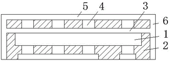
图5为本发明一种芯片散热工艺第二实施例的步骤示意图,包括以下步骤:S1,提供一载板,在晶圆上植球后切割为单一芯片1,将一个或者多个芯片1放置在载板上并包封封装,后暴露出植球;S2,在塑封料上形成与植球连通的焊盘和输出管脚并再次包封封装,后暴露出焊盘和输出管脚,并移走载板;S3,在芯片背面和塑封料表面通过表面处理形成中部导热层3; S4,在中部导热层3远离芯片1的一侧表面处理形成至少一个导热凸起4;S5,包封每个导热凸起4,后暴露出每个导热凸起4远离中部导热层3的一侧,此时整体为封装层2;S6,封装层2远离芯片1焊盘的一侧通过表面处理形成底部散热片5,每个导热凸起4与底部散热片5连接,S7,在封装层2的一侧侧壁、两个侧壁、三个侧壁或者四个侧壁上均设置有侧壁散热片6,形成多面散热,如五面散热,若载板上放置多个芯片1,最后需要进行成品切割工序。
请参阅图7,与实施例一相比,实施例二在原有实施例一的基础上增加了S7,即在多个侧面形成周围金属保护,周围的金属板同样采用电镀或者溅射的方式形成,底部散热片5和封装层2四周的侧壁散热片6在同一步骤形成,侧壁散热片6分别与底部散热片5和中部导热层3连接,侧壁散热片6配合底部散热片5共形成多面金属板,如五面金属板,散热效果更强,且保护性强。
本发明通过继续在多个侧面形成侧壁散热片6,如构成五面散热,同时器件周围形成金属保护,如四周,芯片硅产生的热量通过导热凸起4传递给底部散热片5和侧壁散热片6散热,热传导较快,且芯片两面结构较为对称,能平衡高低温形成的应力作用,器件可靠性增加,且中部导热层3的厚度薄热应力对芯片硅影响较小,底部散热片5的热应力挤压环氧树脂塑封料,避免芯片损坏。
可以理解,本发明是通过一些实施例进行描述的,本领域技术人员知悉的,在不脱离本发明的精神和范围的情况下,可以对这些特征和实施例进行各种改变或等效替换。另外,在本发明的教导下,可以对这些特征和实施例进行修改以适应具体的情况及材料而不会脱离本发明的精神和范围。因此,本发明不受此处所公开的具体实施例的限制,所有落入本申请的权利要求范围内的实施例都属于本发明所保护的范围内。
Claims (8)
1.一种芯片散热结构,包括至少一芯片(1)及封装层(2),
所述封装层(2)包封所述芯片(1),所述芯片(1)的一侧通过电性连接处电性连接有焊盘和输出管脚,所述输出管脚穿过所述封装层(2)与所述芯片(1)电性连接;
其特征在于,所述封装层(2)远离芯片(1)焊盘的一侧整个表面设置有底部散热片(5),所述封装层(2)的内部设置有用以对封装层(2)内部结构产生的变温应力进行缓冲且传导内部热量的中部结构,所述中部结构包括中部导热层(3)和至少一导热凸起(4),芯片(1)将封装层(2)分割为对称的上下两层,且上层封装层包封的多个导热凸起(4)和下层封装层包封的芯片(1)电性连接处结构对称。
2.根据权利要求1所述的芯片散热结构,其特征在于,所述中部结构将芯片(1)背面与底部散热片(5)连接。
3.根据权利要求2所述的芯片散热结构,其特征在于,所述中部导热层(3)设置在芯片(1)背面和此背面对应的封装层(2)的外表面,所述中部导热层(3)的材料为金属铜、钨、镍或钽。
4.根据权利要求2所述的芯片散热结构,其特征在于,每个所述导热凸起(4)设置在中部导热层(3)远离芯片(1)的一侧,每个所述导热凸起(4)的形状为规则圆柱形或长方体形,且倾斜或竖直的设置在中部导热层(3)的表面。
5.根据权利要求4所述的芯片散热结构,其特征在于,每个所述导热凸起(4)远离中部导热层(3)的一端与底部散热片(5)连接。
6.根据权利要求5所述的芯片散热结构,其特征在于,所述中部导热层(3)、导热凸起(4)和底部散热片(5)所形成的方式为电镀或溅射。
7.根据权利要求1所述的芯片散热结构,其特征在于,所述封装层(2)的一个侧壁、两个侧壁、三个侧壁或者四个侧壁上均设置有侧壁散热片(6),所述侧壁散热片(6)分别与底部散热片(5)和中部导热层(3)连接。
8.一种半导体器件,其特征在于,包括权利要求1-7任意一项所述的芯片散热结构。
Priority Applications (2)
| Application Number | Priority Date | Filing Date | Title |
|---|---|---|---|
| CN202210586279.0A CN114678335B (zh) | 2022-05-27 | 2022-05-27 | 一种芯片散热结构、工艺及半导体器件 |
| US18/320,955 US20230386959A1 (en) | 2022-05-27 | 2023-05-19 | Chip heat dissipating structure, process and semiconductor device |
Applications Claiming Priority (1)
| Application Number | Priority Date | Filing Date | Title |
|---|---|---|---|
| CN202210586279.0A CN114678335B (zh) | 2022-05-27 | 2022-05-27 | 一种芯片散热结构、工艺及半导体器件 |
Publications (2)
| Publication Number | Publication Date |
|---|---|
| CN114678335A CN114678335A (zh) | 2022-06-28 |
| CN114678335B true CN114678335B (zh) | 2022-08-16 |
Family
ID=82079812
Family Applications (1)
| Application Number | Title | Priority Date | Filing Date |
|---|---|---|---|
| CN202210586279.0A Active CN114678335B (zh) | 2022-05-27 | 2022-05-27 | 一种芯片散热结构、工艺及半导体器件 |
Country Status (2)
| Country | Link |
|---|---|
| US (1) | US20230386959A1 (zh) |
| CN (1) | CN114678335B (zh) |
Families Citing this family (1)
| Publication number | Priority date | Publication date | Assignee | Title |
|---|---|---|---|---|
| CN118053822B (zh) * | 2024-04-16 | 2024-08-06 | 四川职业技术学院 | 一种电源管理芯片的封装结构及封装方法 |
Citations (4)
| Publication number | Priority date | Publication date | Assignee | Title |
|---|---|---|---|---|
| JP2005093842A (ja) * | 2003-09-19 | 2005-04-07 | Nitto Denko Corp | 放熱シートおよび放熱部材 |
| JP6551566B1 (ja) * | 2018-03-14 | 2019-07-31 | オムロン株式会社 | 電子部品の放熱構造 |
| CN210325766U (zh) * | 2019-09-27 | 2020-04-14 | 深圳市南科芯微电子有限公司 | 一种蓝牙音箱用集成电路的封装结构 |
| CN114220785A (zh) * | 2021-12-16 | 2022-03-22 | 华天科技(南京)有限公司 | 一种具有高可靠度焊点结构的散热倒装封装结构及方法 |
Family Cites Families (4)
| Publication number | Priority date | Publication date | Assignee | Title |
|---|---|---|---|---|
| JP2000150714A (ja) * | 1998-11-09 | 2000-05-30 | Mitsubishi Gas Chem Co Inc | 半導体プラスチックパッケージ用プリント配線板 |
| US20090236732A1 (en) * | 2008-03-19 | 2009-09-24 | Powertech Technology Inc. | Thermally-enhanced multi-hole semiconductor package |
| US20150091154A1 (en) * | 2013-09-30 | 2015-04-02 | Macrotech Technology Inc. | Substrateless packages with scribe disposed on heat spreader |
| US10580715B2 (en) * | 2018-06-14 | 2020-03-03 | Texas Instruments Incorporated | Stress buffer layer in embedded package |
-
2022
- 2022-05-27 CN CN202210586279.0A patent/CN114678335B/zh active Active
-
2023
- 2023-05-19 US US18/320,955 patent/US20230386959A1/en active Pending
Patent Citations (4)
| Publication number | Priority date | Publication date | Assignee | Title |
|---|---|---|---|---|
| JP2005093842A (ja) * | 2003-09-19 | 2005-04-07 | Nitto Denko Corp | 放熱シートおよび放熱部材 |
| JP6551566B1 (ja) * | 2018-03-14 | 2019-07-31 | オムロン株式会社 | 電子部品の放熱構造 |
| CN210325766U (zh) * | 2019-09-27 | 2020-04-14 | 深圳市南科芯微电子有限公司 | 一种蓝牙音箱用集成电路的封装结构 |
| CN114220785A (zh) * | 2021-12-16 | 2022-03-22 | 华天科技(南京)有限公司 | 一种具有高可靠度焊点结构的散热倒装封装结构及方法 |
Also Published As
| Publication number | Publication date |
|---|---|
| CN114678335A (zh) | 2022-06-28 |
| US20230386959A1 (en) | 2023-11-30 |
Similar Documents
| Publication | Publication Date | Title |
|---|---|---|
| US11594469B2 (en) | Semiconductor device and method of manufacture | |
| US20210225805A1 (en) | Semiconductor device assemblies with molded support substrates | |
| US7202561B2 (en) | Semiconductor package with heat dissipating structure and method of manufacturing the same | |
| JP6122863B2 (ja) | 複数の熱経路を備える積み重ねられた半導体ダイアセンブリ、ならびに関連するシステムおよび方法 | |
| US11387159B2 (en) | Chip package | |
| US20130069218A1 (en) | High density package interconnect with copper heat spreader and method of making the same | |
| EP2111636B1 (en) | High thermal performance packaging for circuit dies | |
| US9666506B2 (en) | Heat spreader with wiring substrate for reduced thickness | |
| JP2000156436A (ja) | 半導体素子および半導体チップのパッケ―ジ方法 | |
| US20100052156A1 (en) | Chip scale package structure and fabrication method thereof | |
| CN114678335B (zh) | 一种芯片散热结构、工艺及半导体器件 | |
| CN110808233A (zh) | 一种用于系统散热的封装结构及其封装工艺 | |
| TWI536515B (zh) | 具有散熱結構之半導體封裝元件及其封裝方法 | |
| TWI237363B (en) | Semiconductor package | |
| CN212434607U (zh) | 基于圆片重构工艺的三维堆叠封装散热结构 | |
| TWI521654B (zh) | 半導體裝置及製造半導體裝置的方法 | |
| TWI721898B (zh) | 半導體封裝結構 | |
| US9230874B1 (en) | Integrated circuit package with a heat conductor | |
| KR100712499B1 (ko) | 열 배출 효율이 증대된 멀티 칩 패키지 및 그 제조방법 | |
| TWI755319B (zh) | 晶片封裝結構 | |
| TWI355723B (en) | Heat spreader chip scale package and method for ma | |
| KR20240085677A (ko) | 반도체 패키지 및 그 제조 방법 | |
| TW202245176A (zh) | 具有高散熱效能的半導體裝置 | |
| JP2003258163A (ja) | 半導体装置 |
Legal Events
| Date | Code | Title | Description |
|---|---|---|---|
| PB01 | Publication | ||
| PB01 | Publication | ||
| SE01 | Entry into force of request for substantive examination | ||
| SE01 | Entry into force of request for substantive examination | ||
| GR01 | Patent grant | ||
| GR01 | Patent grant |