US10344395B2 - Apparatus and method for growing silicon single crystal ingot - Google Patents
Apparatus and method for growing silicon single crystal ingot Download PDFInfo
- Publication number
- US10344395B2 US10344395B2 US15/564,045 US201615564045A US10344395B2 US 10344395 B2 US10344395 B2 US 10344395B2 US 201615564045 A US201615564045 A US 201615564045A US 10344395 B2 US10344395 B2 US 10344395B2
- Authority
- US
- United States
- Prior art keywords
- crucible
- ingot
- silicon melt
- single crystal
- silicon
- Prior art date
- Legal status (The legal status is an assumption and is not a legal conclusion. Google has not performed a legal analysis and makes no representation as to the accuracy of the status listed.)
- Active
Links
- XUIMIQQOPSSXEZ-UHFFFAOYSA-N Silicon Chemical compound [Si] XUIMIQQOPSSXEZ-UHFFFAOYSA-N 0.000 title claims abstract description 92
- 229910052710 silicon Inorganic materials 0.000 title claims abstract description 92
- 239000010703 silicon Substances 0.000 title claims abstract description 92
- 239000013078 crystal Substances 0.000 title claims abstract description 59
- 238000000034 method Methods 0.000 title claims description 45
- 238000009792 diffusion process Methods 0.000 claims description 19
- 238000010438 heat treatment Methods 0.000 claims description 2
- QVGXLLKOCUKJST-UHFFFAOYSA-N atomic oxygen Chemical compound [O] QVGXLLKOCUKJST-UHFFFAOYSA-N 0.000 description 27
- 239000001301 oxygen Substances 0.000 description 27
- 229910052760 oxygen Inorganic materials 0.000 description 27
- 235000012431 wafers Nutrition 0.000 description 20
- 230000000052 comparative effect Effects 0.000 description 7
- 238000004519 manufacturing process Methods 0.000 description 7
- 238000010586 diagram Methods 0.000 description 6
- 239000002019 doping agent Substances 0.000 description 4
- OKTJSMMVPCPJKN-UHFFFAOYSA-N Carbon Chemical compound [C] OKTJSMMVPCPJKN-UHFFFAOYSA-N 0.000 description 3
- 238000005247 gettering Methods 0.000 description 3
- 239000000155 melt Substances 0.000 description 3
- 239000004065 semiconductor Substances 0.000 description 3
- XKRFYHLGVUSROY-UHFFFAOYSA-N Argon Chemical compound [Ar] XKRFYHLGVUSROY-UHFFFAOYSA-N 0.000 description 2
- IJGRMHOSHXDMSA-UHFFFAOYSA-N Atomic nitrogen Chemical compound N#N IJGRMHOSHXDMSA-UHFFFAOYSA-N 0.000 description 2
- 238000009826 distribution Methods 0.000 description 2
- 229910002804 graphite Inorganic materials 0.000 description 2
- 239000010439 graphite Substances 0.000 description 2
- 238000005498 polishing Methods 0.000 description 2
- 229910021420 polycrystalline silicon Inorganic materials 0.000 description 2
- 239000002244 precipitate Substances 0.000 description 2
- 239000010453 quartz Substances 0.000 description 2
- VYPSYNLAJGMNEJ-UHFFFAOYSA-N silicon dioxide Inorganic materials O=[Si]=O VYPSYNLAJGMNEJ-UHFFFAOYSA-N 0.000 description 2
- ZOXJGFHDIHLPTG-UHFFFAOYSA-N Boron Chemical compound [B] ZOXJGFHDIHLPTG-UHFFFAOYSA-N 0.000 description 1
- OAICVXFJPJFONN-UHFFFAOYSA-N Phosphorus Chemical compound [P] OAICVXFJPJFONN-UHFFFAOYSA-N 0.000 description 1
- 229910052787 antimony Inorganic materials 0.000 description 1
- WATWJIUSRGPENY-UHFFFAOYSA-N antimony atom Chemical compound [Sb] WATWJIUSRGPENY-UHFFFAOYSA-N 0.000 description 1
- 229910052786 argon Inorganic materials 0.000 description 1
- 229910052785 arsenic Inorganic materials 0.000 description 1
- RQNWIZPPADIBDY-UHFFFAOYSA-N arsenic atom Chemical compound [As] RQNWIZPPADIBDY-UHFFFAOYSA-N 0.000 description 1
- 230000009286 beneficial effect Effects 0.000 description 1
- 210000000746 body region Anatomy 0.000 description 1
- 229910052796 boron Inorganic materials 0.000 description 1
- 229910052799 carbon Inorganic materials 0.000 description 1
- 238000004140 cleaning Methods 0.000 description 1
- 238000005336 cracking Methods 0.000 description 1
- 238000002425 crystallisation Methods 0.000 description 1
- 230000008025 crystallization Effects 0.000 description 1
- 230000007547 defect Effects 0.000 description 1
- 239000006185 dispersion Substances 0.000 description 1
- 230000000694 effects Effects 0.000 description 1
- 239000007789 gas Substances 0.000 description 1
- 239000012535 impurity Substances 0.000 description 1
- 239000012212 insulator Substances 0.000 description 1
- 239000007788 liquid Substances 0.000 description 1
- 238000003754 machining Methods 0.000 description 1
- 239000000463 material Substances 0.000 description 1
- 238000002844 melting Methods 0.000 description 1
- 230000008018 melting Effects 0.000 description 1
- 229910052751 metal Inorganic materials 0.000 description 1
- 239000002184 metal Substances 0.000 description 1
- 229910021421 monocrystalline silicon Inorganic materials 0.000 description 1
- 229910052757 nitrogen Inorganic materials 0.000 description 1
- 230000002093 peripheral effect Effects 0.000 description 1
- 229910052698 phosphorus Inorganic materials 0.000 description 1
- 239000011574 phosphorus Substances 0.000 description 1
- 238000007517 polishing process Methods 0.000 description 1
- 230000003014 reinforcing effect Effects 0.000 description 1
- 239000000126 substance Substances 0.000 description 1
Images


Classifications
-
- C—CHEMISTRY; METALLURGY
- C30—CRYSTAL GROWTH
- C30B—SINGLE-CRYSTAL GROWTH; UNIDIRECTIONAL SOLIDIFICATION OF EUTECTIC MATERIAL OR UNIDIRECTIONAL DEMIXING OF EUTECTOID MATERIAL; REFINING BY ZONE-MELTING OF MATERIAL; PRODUCTION OF A HOMOGENEOUS POLYCRYSTALLINE MATERIAL WITH DEFINED STRUCTURE; SINGLE CRYSTALS OR HOMOGENEOUS POLYCRYSTALLINE MATERIAL WITH DEFINED STRUCTURE; AFTER-TREATMENT OF SINGLE CRYSTALS OR A HOMOGENEOUS POLYCRYSTALLINE MATERIAL WITH DEFINED STRUCTURE; APPARATUS THEREFOR
- C30B15/00—Single-crystal growth by pulling from a melt, e.g. Czochralski method
- C30B15/10—Crucibles or containers for supporting the melt
-
- C—CHEMISTRY; METALLURGY
- C30—CRYSTAL GROWTH
- C30B—SINGLE-CRYSTAL GROWTH; UNIDIRECTIONAL SOLIDIFICATION OF EUTECTIC MATERIAL OR UNIDIRECTIONAL DEMIXING OF EUTECTOID MATERIAL; REFINING BY ZONE-MELTING OF MATERIAL; PRODUCTION OF A HOMOGENEOUS POLYCRYSTALLINE MATERIAL WITH DEFINED STRUCTURE; SINGLE CRYSTALS OR HOMOGENEOUS POLYCRYSTALLINE MATERIAL WITH DEFINED STRUCTURE; AFTER-TREATMENT OF SINGLE CRYSTALS OR A HOMOGENEOUS POLYCRYSTALLINE MATERIAL WITH DEFINED STRUCTURE; APPARATUS THEREFOR
- C30B15/00—Single-crystal growth by pulling from a melt, e.g. Czochralski method
- C30B15/14—Heating of the melt or the crystallised materials
-
- C—CHEMISTRY; METALLURGY
- C30—CRYSTAL GROWTH
- C30B—SINGLE-CRYSTAL GROWTH; UNIDIRECTIONAL SOLIDIFICATION OF EUTECTIC MATERIAL OR UNIDIRECTIONAL DEMIXING OF EUTECTOID MATERIAL; REFINING BY ZONE-MELTING OF MATERIAL; PRODUCTION OF A HOMOGENEOUS POLYCRYSTALLINE MATERIAL WITH DEFINED STRUCTURE; SINGLE CRYSTALS OR HOMOGENEOUS POLYCRYSTALLINE MATERIAL WITH DEFINED STRUCTURE; AFTER-TREATMENT OF SINGLE CRYSTALS OR A HOMOGENEOUS POLYCRYSTALLINE MATERIAL WITH DEFINED STRUCTURE; APPARATUS THEREFOR
- C30B15/00—Single-crystal growth by pulling from a melt, e.g. Czochralski method
- C30B15/20—Controlling or regulating
-
- C—CHEMISTRY; METALLURGY
- C30—CRYSTAL GROWTH
- C30B—SINGLE-CRYSTAL GROWTH; UNIDIRECTIONAL SOLIDIFICATION OF EUTECTIC MATERIAL OR UNIDIRECTIONAL DEMIXING OF EUTECTOID MATERIAL; REFINING BY ZONE-MELTING OF MATERIAL; PRODUCTION OF A HOMOGENEOUS POLYCRYSTALLINE MATERIAL WITH DEFINED STRUCTURE; SINGLE CRYSTALS OR HOMOGENEOUS POLYCRYSTALLINE MATERIAL WITH DEFINED STRUCTURE; AFTER-TREATMENT OF SINGLE CRYSTALS OR A HOMOGENEOUS POLYCRYSTALLINE MATERIAL WITH DEFINED STRUCTURE; APPARATUS THEREFOR
- C30B15/00—Single-crystal growth by pulling from a melt, e.g. Czochralski method
- C30B15/30—Mechanisms for rotating or moving either the melt or the crystal
- C30B15/305—Stirring of the melt
-
- C—CHEMISTRY; METALLURGY
- C30—CRYSTAL GROWTH
- C30B—SINGLE-CRYSTAL GROWTH; UNIDIRECTIONAL SOLIDIFICATION OF EUTECTIC MATERIAL OR UNIDIRECTIONAL DEMIXING OF EUTECTOID MATERIAL; REFINING BY ZONE-MELTING OF MATERIAL; PRODUCTION OF A HOMOGENEOUS POLYCRYSTALLINE MATERIAL WITH DEFINED STRUCTURE; SINGLE CRYSTALS OR HOMOGENEOUS POLYCRYSTALLINE MATERIAL WITH DEFINED STRUCTURE; AFTER-TREATMENT OF SINGLE CRYSTALS OR A HOMOGENEOUS POLYCRYSTALLINE MATERIAL WITH DEFINED STRUCTURE; APPARATUS THEREFOR
- C30B29/00—Single crystals or homogeneous polycrystalline material with defined structure characterised by the material or by their shape
- C30B29/02—Elements
- C30B29/06—Silicon
Definitions
- the embodiment relates to an apparatus and a method for growing a silicon single crystal ingot and more particularly, is to secure a uniformity of oxygen concentration in diameter and radial directions in a silicon single crystal ingot.
- a silicon wafer is formed by a single crystal growing process for manufacturing a single crystal ingot, a slicing process for obtaining a thin disk-shaped wafer by slicing the single crystal ingot, a grinding process for machining an outer peripheral portion of a wafer to prevent cracking and distortion of the wafer obtained by the slicing process, a lapping process for removing damages due to mechanical processing remaining on the wafer, a polishing process for polishing the wafer, and a cleaning process for removing an abrasive or an foreign substance adhering to the wafer while polishing the polished wafer.
- CZ method For a single crystal growth, a floating zone (FZ) method or a Czochralski (CZ) method (hereinafter referred to as CZ method) has been widely used.
- the CZ method is the most common method among these methods.
- a polycrystalline silicon is charged in a quartz crucible and heated and melted by a graphite heating element, and then a single crystal silicon ingot is grown by pulling up a seed crystal while rotating the seed crystal when the seed crystal is immersed in silicon melt formed as a result of melting and crystallization occurs at an interface.
- oxygen is included in a silicon single crystal as crystal defects due to growth history and undesired impurities in a growing process of the silicon single crystal, and thus intruded oxygen in this manner is grown into oxygen precipitate due to heat applied during a manufacturing process of a semiconductor device.
- the oxygen precipitate shows beneficial characteristics such as reinforcing the strength of the silicon wafer and capturing metal pollution elements and serving as an internal gettering site, a leakage current and a fail of the semiconductor device are caused.
- oxygen concentration of a wafer manufactured from the silicon single crystal ingot needs to be uniform in longitudinal and radial directions, and the oxygen concentration may be controlled through a seed rotating speed, a crucible rotating speed, a melt gap, which is the distance between a melt surface and a heat shield, a pull speed of the ingot, a design change of hot zone, a third element doping such as nitrogen or carbon, which are process variables when growing a silicon single crystal ingot.
- the embodiment is directed to providing a method for growing a silicon single crystal to secure a uniformity of oxygen concentration in longitudinal and radial directions.
- An embodiment provides an apparatus for growing a silicon single crystal ingot, including: a chamber; a crucible provided inside the chamber to accommodate silicon melt; a rotating shaft and a crucible support disposed at a lower portion of the crucible; a heater provided inside the chamber to heat the silicon melt; a pulling unit for rotating and pulling up an ingot grown from the silicon melt; and a magnetic field generating unit for applying a horizontal magnetic field to the crucible, wherein a first direction in which the rotating shaft rotates the crucible and a second direction in which the pulling unit rotates the ingot are the same.
- the heater may heat the periphery of the crucible so that a maximum heat generating position is formed below a maximum gauss position (MGP).
- MGP maximum gauss position
- the heater may heat the periphery of the crucible so that a maximum heat generating position is formed at 100 to 200 mm below the MGP.
- the heater and the pulling unit may heat the crucible so that a diffusion boundary layer is uniformly distributed at an edge of a radial direction of the silicon melt and may pull up the ingot.
- the heater and the pulling unit may heat the crucible so that the diffusion boundary layer is formed at 12 mm below a surface of the silicon melt and may pull up the ingot.
- the heater and the pulling unit may heat the crucible so that the diffusion boundary layer is distributed over a diameter of 300 mm or more from an edge of the silicon melt and may pull up the ingot.
- Another embodiment is directed to providing a method for growing a silicon single crystal ingot in which an ingot and a crucible are rotated in the same direction and a maximum heat generating position is below a maximum gauss position (MGP).
- MGP maximum gauss position
- a diffusion boundary layer may be uniformly distributed at an edge in a radial direction of silicon melt.
- the diffusion boundary layer may be distributed 12 mm below a surface of the silicon melt, in a region of diameter of 300 mm or more.
- a flow of the silicon melt may be constant in a depth direction in the silicon melt.
- a maximum heat generating position may be located 100 to 200 mm lower than the MGP.
- the flow of the silicon melt may be constant, the diffusion boundary layer may be distributed at an edge of the ingot, and the oxygen concentration of the manufactured silicon wafer may be constant, and thus resistivity may be improved.
- FIG. 1 is a view illustrating an apparatus of manufacturing a single crystal ingot according to an embodiment
- FIG. 2 is a diagram illustrating a shift of a maximum gauss position (MGP) at the time of growing a silicon single crystal ingot
- FIG. 3 is a view illustrating a conventional maximum heat generating position and a maximum heat generating position according to an embodiment
- FIGS. 4A to 4C are views illustrating a flow of silicon melt together with a comparative example in a method for growing a silicon single crystal ingot according to an embodiment
- FIGS. 5A to 5C are views illustrating a distribution of oxygen in silicon melt together with a comparative example in a method for growing a silicon single crystal ingot according to an embodiment
- FIG. 6A is a diagram illustrating a uniformity of oxygen concentration in a method for growing a silicon single crystal ingot according to an embodiment
- FIG. 6B is a diagram illustrating a uniformity of oxygen concentration in a method for growing a silicon single crystal ingot according to a comparative example.
- relational terms such as “first” and “second,” “over/upper portion/above,” and “below/lower portion/under” do not necessarily require or include any physical or logical relationship or sequence between devices or elements, and may also be used only to distinguish one device or element from another device or element.
- Thicknesses of layers and areas in the drawings may be exaggerated, omitted, or schematically described for a convenient and precise description.
- the size of each component does not fully match the actual size thereof.
- FIG. 1 is a view illustrating an apparatus of manufacturing a single crystal ingot according to an embodiment.
- an apparatus of manufacturing a silicon single crystal ingot 100 may include a chamber 110 , a crucible 120 , a heater 130 , a pulling unit 150 , and the like.
- an apparatus of manufacturing a silicon single crystal ingot 100 according to the embodiment may include the chamber 110 , the crucible 120 provided in the chamber 110 to receive a silicon melt, the heater 130 provided in the chamber 110 and configured to heat the crucible 120 , and a pulling unit 150 coupled to a seed crystal 152 at one end thereof, and a magnetic field generating unit (not shown) to apply a horizontal magnetic field to the crucible 120 .
- the chamber 110 provides a space in which predetermined processes for growing the single crystal ingot for a silicon wafer used as an electronic component material such as a semiconductor are performed.
- a radiant insulator 140 may be installed on an inner wall of the chamber 110 to prevent heat of the heater 130 from being radiated to a side wall of the chamber 110 .
- argon gas or the like may be injected into the chamber 110 of the silicon single crystal growing apparatus to control the oxygen concentration and then be discharged downward.
- the crucible 120 is provided inside the chamber 110 to contain silicon melt and may be made of quartz or the like.
- a crucible support (not shown) made of graphite may be provided on the outside of the crucible 120 to support the crucible 120 .
- the crucible support is fixedly installed on a rotating shaft (not shown), and the rotating shaft is rotated by a driving unit (not shown) to rotate and elevate the crucible 120 , so that a solid-liquid interface, that is, the interface between the solidified ingot and the silicon melt, may maintain the same height.
- the rotating shaft may rotate in a first direction for rotating the crucible
- the pulling unit may rotate in a second direction for rotating the ingot, wherein the first direction and the second direction may be the same.
- the heater 130 may be provided inside the chamber 110 to heat the crucible 120 .
- the heater 130 may have a cylindrical shape surrounding the crucible support.
- the heater 130 melts a high-purity polycrystalline silicon ingot placed in the crucible 120 which may be formed into silicon melt.
- the crucible 120 is heated by heat supplied from the heater 130 .
- the temperature in each region may vary depending on the height of the crucible 120 , and a region having the highest temperature may correspond to a maximum heat generating position of the heater 130 .
- a Czochralski (CZ) method for growing a crystal by immersing a seed crystal 152 which is a single crystal in silicon melt and slowly pulling up the seed crystal 152 to grow a crystal may be employed.
- the CZ method is described in detail as follows.
- a necking process is performed to grow elongated crystals from the seed crystal 152 , then the crystal is grown in a diameter direction and subjected to a shouldering process to make a target diameter, after a body growing process is performed to grow crystals having a predetermined diameter, after the body growing has progressed by a certain length, the diameter of the crystal is gradually reduced, and finally a tailing process is performed to separate the crystal from the molten silicon, thereby completing the growth of the single crystal.
- B which is a P-type dopant and As (arsenic), P (phosphorus), Sb (antimony) or the like, which are N-type dopants, may be doped in the silicon melt.
- V/G growth rate/temperature gradient
- oxygen concentration may be changed within an interior, particularly a body region of the ingot.
- an ingot and a crucible are rotated in the same direction at the time of growing the ingot, a heater is arranged so that a maximum heat generating position is below a maximum gauss position (MGP), and thus oxygen concentration in longitudinal and radial directions (in-plane direction) of the ingot may be constant, and resistivity of the wafer to be produced may be constant.
- MGP maximum gauss position
- a magnetic field is applied to the periphery of the crucible 120 by the magnetic field applying unit, and a region having the strongest magnetic field intensity may be referred to as a maximum gauss position (MGP).
- MGP maximum gauss position
- the heater and the magnetic field may heat the periphery of the crucible 120 and apply a magnetic field to the periphery of the crucible so that a maximum heat generating position is formed below the maximum gauss position (MGP).
- the maximum heat generating position may be formed at a position 100 to 200 mm below the MGP.
- FIG. 2 is a diagram illustrating a shift of a maximum gauss position (MGP) at the time of growth of a silicon single crystal ingot.
- MGP maximum gauss position
- a maximum gauss point may move up and down from an interface between ‘A’, which is a region inside the crucible, and ‘B’, which is a region of an upper chamber, and the MGP may move within a range of ‘a’ in the ‘A’ direction and ‘b’ in the ‘B’ direction from the above interface.
- the maximum heat generating position of the heater may be lower than the MGP described above.
- FIG. 3 is a view illustrating a conventional maximum heat generating position and a maximum heat generating position according to an embodiment.
- a maximum heat generating position is at a lower portion than that of the related art and in particular, the maximum heat generating position may be at a distance D of 100 to 200 mm lower than the MGP. At this point, a flow of the silicon melt may be changed.
- the flow above the silicon melt may become a turbulence, and if the maximum heat generating position is below to 100 mm, the flow under the silicon melt may become a turbulence.
- a maximum heat generating position may be at 100 mm to 200 mm below the MGP so that the flow in a depth direction of the silicon melt, that is, in the vertical direction in FIG. 1 , may be constant.
- a diffusion boundary layer may be distributed at a depth of about 12 mm from a surface of the growing silicon melt, in a region outside the diameter of about 300 mm.
- the diffusion boundary layer in the silicon melt may be uniformly distributed at an edge of a radial direction, and the diffusion boundary layer may be confirmed by measuring the temperature of the silicon melt.
- the heater and the pulling unit may heat the crucible so that a diffusion boundary layer is uniformly distributed at an edge of the radial direction of the silicon melt and may pull up the ingot.
- the heater and the pulling unit may heat the crucible so that the diffusion boundary layer is formed at 12 mm below a surface of the silicon melt and may pull up the ingot.
- a diffusion boundary layer is a region having a diffusion rate of about 10 ⁇ 8 m 2 /sec. In the embodiment, at a temperature of about 1700 Kelvin, the diffusion boundary layer may be at the maximum diameter of 320 mm.
- FIGS. 4A to 4C are views illustrating a flow of silicon melt together with a comparative example in a method for growing a silicon single crystal ingot according to an embodiment.
- a left side illustrates a flow of the silicon melt on a surface of the silicon melt and a flow in a lower region toward the right side
- the utmost right side represents a flow of the silicon melt at the bottom surface of the crucible.
- a pattern of flow of the silicon melt is maintained in the lower region.
- a pattern of flow of the silicon melt may be blurred at the bottom.
- FIGS. 5A to 5C are views illustrating a distribution of oxygen in silicon melt together with a comparative example in a method for growing a silicon single crystal ingot according to an embodiment.
- a diffusion boundary layer is maintained at an edge of the ingot and a variation in speed of the silicon melt is suppressed so that oxygen concentration is uniform up to 2200 mm in a depth direction.
- a flow of the silicon melt is not constant and the oxygen concentration may not be uniform at 2000 mm in the depth direction.
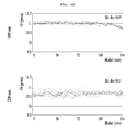
- FIG. 6A is a diagram illustrating a uniformity of oxygen concentration in a method for growing a silicon single crystal ingot according to an embodiment
- FIG. 6B is a diagram illustrating a uniformity of oxygen concentration in a method for growing a silicon single crystal ingot according to a comparative example.
- silicon wafers are 1800 and 2200 mm in length, respectively and 0.09 and 0.11 in resistivity, respectively, and oxygen concentration of the silicon wafers manufactured from one ingot is almost uniform in a radial direction.
- silicon wafers are 1100 and 1800 mm in length and 0.16 and 0.19 in resistivity, respectively, and oxygen concentration of the silicon wafers manufactured from one ingot represents a large dispersion in a radial direction.
- a flow of the silicon melt may be constant, so that the diffusion boundary layer may be distributed at an edge of the ingot, and the oxygen concentration of the manufactured silicon wafer may be constant, and thus resistivity may be improved.
- an apparatus and method for growing a silicon single crystal ingot may improve a uniformity of oxygen concentration in diameter and radial directions in the silicon single crystal ingot.
Landscapes
- Chemical & Material Sciences (AREA)
- Engineering & Computer Science (AREA)
- Crystallography & Structural Chemistry (AREA)
- Materials Engineering (AREA)
- Metallurgy (AREA)
- Organic Chemistry (AREA)
- Crystals, And After-Treatments Of Crystals (AREA)
- Physics & Mathematics (AREA)
- Condensed Matter Physics & Semiconductors (AREA)
- General Physics & Mathematics (AREA)
- Manufacturing & Machinery (AREA)
- Computer Hardware Design (AREA)
- Microelectronics & Electronic Packaging (AREA)
- Power Engineering (AREA)
Applications Claiming Priority (3)
| Application Number | Priority Date | Filing Date | Title |
|---|---|---|---|
| KR1020150052307A KR101729515B1 (ko) | 2015-04-14 | 2015-04-14 | 실리콘 단결정 잉곳의 성장 방법 |
| KR10-2015-0052307 | 2015-04-14 | ||
| PCT/KR2016/003841 WO2016167542A1 (ko) | 2015-04-14 | 2016-04-12 | 실리콘 단결정 잉곳의 성장 장치 및 방법 |
Publications (2)
| Publication Number | Publication Date |
|---|---|
| US20180094359A1 US20180094359A1 (en) | 2018-04-05 |
| US10344395B2 true US10344395B2 (en) | 2019-07-09 |
Family
ID=57127285
Family Applications (1)
| Application Number | Title | Priority Date | Filing Date |
|---|---|---|---|
| US15/564,045 Active US10344395B2 (en) | 2015-04-14 | 2016-04-12 | Apparatus and method for growing silicon single crystal ingot |
Country Status (4)
| Country | Link |
|---|---|
| US (1) | US10344395B2 (enExample) |
| JP (1) | JP2018510839A (enExample) |
| KR (1) | KR101729515B1 (enExample) |
| WO (1) | WO2016167542A1 (enExample) |
Families Citing this family (4)
| Publication number | Priority date | Publication date | Assignee | Title |
|---|---|---|---|---|
| JP7342845B2 (ja) * | 2020-11-25 | 2023-09-12 | 株式会社Sumco | シリコン単結晶の製造方法 |
| US12486593B2 (en) | 2022-08-29 | 2025-12-02 | Globalwafers Co., Ltd. | Axial positioning of magnetic poles while producing a silicon ingot |
| US12486594B2 (en) | 2022-08-29 | 2025-12-02 | Globalwafers Co., Ltd. | Ingot puller apparatus that axially position magnetic poles |
| CN117364225B (zh) * | 2023-12-07 | 2024-02-23 | 天通控股股份有限公司 | 一种晶体与坩埚同向旋转的长晶方法 |
Citations (16)
| Publication number | Priority date | Publication date | Assignee | Title |
|---|---|---|---|---|
| US5306387A (en) * | 1990-06-21 | 1994-04-26 | Shin-Etsu Handotai Co., Ltd. | Method for pulling up semiconductor single crystal |
| JPH08231294A (ja) | 1995-02-24 | 1996-09-10 | Toshiba Ceramics Co Ltd | 水平磁界下シリコン単結晶引上方法 |
| JPH09208385A (ja) | 1996-01-30 | 1997-08-12 | Mitsubishi Materials Corp | シリコン単結晶の育成方法及びその装置 |
| KR100239864B1 (ko) | 1995-06-01 | 2000-01-15 | 와다 다다시 | 단결정의 제조방법 및 장치 |
| JP2003321297A (ja) | 2002-04-25 | 2003-11-11 | Shin Etsu Handotai Co Ltd | シリコン単結晶の製造方法及びシリコン単結晶ウェーハ |
| JP2005015314A (ja) | 2003-06-27 | 2005-01-20 | Shin Etsu Handotai Co Ltd | 単結晶の製造方法及び単結晶 |
| JP2007084417A (ja) | 2005-09-21 | 2007-04-05 | Siltron Inc | 高品質シリコン単結晶インゴットの成長装置,その装置を利用した成長方法 |
| JP2008019129A (ja) | 2006-07-13 | 2008-01-31 | Sumco Corp | 単結晶製造装置、単結晶の製造方法および単結晶 |
| JP2008214118A (ja) | 2007-03-01 | 2008-09-18 | Shin Etsu Handotai Co Ltd | 半導体単結晶の製造方法 |
| US20080286565A1 (en) * | 2006-11-06 | 2008-11-20 | Yasuo Koike | Method For Manufacturing Epitaxial wafer |
| JP2010024120A (ja) | 2008-07-24 | 2010-02-04 | Sumco Corp | シリコン単結晶およびその育成方法 |
| KR100954291B1 (ko) | 2008-01-21 | 2010-04-26 | 주식회사 실트론 | 고품질의 반도체 단결정 잉곳 제조장치 및 방법 |
| KR20100089457A (ko) | 2009-02-04 | 2010-08-12 | 주식회사 실트론 | 공정 변동이 최소화된 단결정 제조방법 |
| WO2013176396A1 (ko) | 2012-05-23 | 2013-11-28 | 주식회사 엘지실트론 | 단결정 실리콘 잉곳 및 웨이퍼, 그 잉곳 성장 장치 및 방법 |
| KR101379798B1 (ko) | 2012-05-23 | 2014-04-01 | 주식회사 엘지실트론 | 단결정 실리콘 잉곳 성장 장치 및 방법 |
| JP2014214067A (ja) | 2013-04-26 | 2014-11-17 | 信越半導体株式会社 | シリコン単結晶の製造方法 |
Family Cites Families (1)
| Publication number | Priority date | Publication date | Assignee | Title |
|---|---|---|---|---|
| KR20150007885A (ko) * | 2013-07-12 | 2015-01-21 | 엘지이노텍 주식회사 | 형광체 및 이를 구비한 발광 소자 |
-
2015
- 2015-04-14 KR KR1020150052307A patent/KR101729515B1/ko active Active
-
2016
- 2016-04-12 JP JP2018504631A patent/JP2018510839A/ja active Pending
- 2016-04-12 WO PCT/KR2016/003841 patent/WO2016167542A1/ko not_active Ceased
- 2016-04-12 US US15/564,045 patent/US10344395B2/en active Active
Patent Citations (17)
| Publication number | Priority date | Publication date | Assignee | Title |
|---|---|---|---|---|
| US5306387A (en) * | 1990-06-21 | 1994-04-26 | Shin-Etsu Handotai Co., Ltd. | Method for pulling up semiconductor single crystal |
| JPH08231294A (ja) | 1995-02-24 | 1996-09-10 | Toshiba Ceramics Co Ltd | 水平磁界下シリコン単結晶引上方法 |
| KR100239864B1 (ko) | 1995-06-01 | 2000-01-15 | 와다 다다시 | 단결정의 제조방법 및 장치 |
| JPH09208385A (ja) | 1996-01-30 | 1997-08-12 | Mitsubishi Materials Corp | シリコン単結晶の育成方法及びその装置 |
| JP2003321297A (ja) | 2002-04-25 | 2003-11-11 | Shin Etsu Handotai Co Ltd | シリコン単結晶の製造方法及びシリコン単結晶ウェーハ |
| JP2005015314A (ja) | 2003-06-27 | 2005-01-20 | Shin Etsu Handotai Co Ltd | 単結晶の製造方法及び単結晶 |
| JP2007084417A (ja) | 2005-09-21 | 2007-04-05 | Siltron Inc | 高品質シリコン単結晶インゴットの成長装置,その装置を利用した成長方法 |
| JP2008019129A (ja) | 2006-07-13 | 2008-01-31 | Sumco Corp | 単結晶製造装置、単結晶の製造方法および単結晶 |
| US20080286565A1 (en) * | 2006-11-06 | 2008-11-20 | Yasuo Koike | Method For Manufacturing Epitaxial wafer |
| JP2008214118A (ja) | 2007-03-01 | 2008-09-18 | Shin Etsu Handotai Co Ltd | 半導体単結晶の製造方法 |
| KR100954291B1 (ko) | 2008-01-21 | 2010-04-26 | 주식회사 실트론 | 고품질의 반도체 단결정 잉곳 제조장치 및 방법 |
| JP2010024120A (ja) | 2008-07-24 | 2010-02-04 | Sumco Corp | シリコン単結晶およびその育成方法 |
| KR20100089457A (ko) | 2009-02-04 | 2010-08-12 | 주식회사 실트론 | 공정 변동이 최소화된 단결정 제조방법 |
| WO2013176396A1 (ko) | 2012-05-23 | 2013-11-28 | 주식회사 엘지실트론 | 단결정 실리콘 잉곳 및 웨이퍼, 그 잉곳 성장 장치 및 방법 |
| KR101379798B1 (ko) | 2012-05-23 | 2014-04-01 | 주식회사 엘지실트론 | 단결정 실리콘 잉곳 성장 장치 및 방법 |
| US20150147258A1 (en) * | 2012-05-23 | 2015-05-28 | LG SILTRON INCORPORATION a corporation | Single crystal silicon ingot and wafer, and apparatus and method for growing said ingot |
| JP2014214067A (ja) | 2013-04-26 | 2014-11-17 | 信越半導体株式会社 | シリコン単結晶の製造方法 |
Non-Patent Citations (2)
| Title |
|---|
| International Search Report (with English Translation) and Written Opinion dated Jul. 22, 2016 issued in Application No. PCT/KR2016/003841. |
| Japanese Office Action issued in Application 2018-504631 dated Feb. 20, 2019. |
Also Published As
| Publication number | Publication date |
|---|---|
| US20180094359A1 (en) | 2018-04-05 |
| JP2018510839A (ja) | 2018-04-19 |
| WO2016167542A1 (ko) | 2016-10-20 |
| KR20160122453A (ko) | 2016-10-24 |
| KR101729515B1 (ko) | 2017-04-24 |
Similar Documents
| Publication | Publication Date | Title |
|---|---|---|
| US20170362736A1 (en) | Apparatus and method for growing silicon single crystal ingot | |
| KR101303422B1 (ko) | 단결정 잉곳의 제조방법 및 이에 의해 제조된 단결정 잉곳과 웨이퍼 | |
| US10344395B2 (en) | Apparatus and method for growing silicon single crystal ingot | |
| US9469917B2 (en) | Dopant feeder of ignot growing apparatus | |
| JP4367213B2 (ja) | シリコン単結晶の製造方法 | |
| KR101942322B1 (ko) | 단결정 잉곳 성장 장치 및 이를 이용한 단결정 잉곳의 성장 방법 | |
| JP4193610B2 (ja) | 単結晶の製造方法 | |
| JP6107308B2 (ja) | シリコン単結晶製造方法 | |
| CN109415843B (zh) | 单晶硅的制造方法 | |
| JP2004315258A (ja) | 単結晶の製造方法 | |
| US20150044467A1 (en) | Method of growing ingot and ingot | |
| WO2005080646A1 (ja) | 単結晶半導体の製造方法 | |
| KR20170088120A (ko) | 단결정 잉곳 성장장치 및 그 성장방법 | |
| KR102799141B1 (ko) | 단결정 실리콘으로부터 에피택셜 코팅된 반도체 웨이퍼를 생성하는 방법 | |
| JP2009274903A (ja) | シリコン単結晶及びシリコンウェーハの製造方法並びに該方法により製造されたシリコンウェーハ | |
| JP5668786B2 (ja) | シリコン単結晶の育成方法及びシリコンウェーハの製造方法 | |
| KR101741101B1 (ko) | 실리콘 단결정 잉곳 및 그 제조방법 | |
| JP4655861B2 (ja) | 電子デバイス用基板の製造方法 | |
| JP2004269335A (ja) | 単結晶の製造方法 | |
| KR101625431B1 (ko) | 쵸크랄스키법을 이용한 실리콘 단결정의 성장 방법 및 실리콘 단결정 잉곳 | |
| JP2002075924A (ja) | シリコン単結晶インゴットの加工方法 | |
| KR101193678B1 (ko) | 대구경 단결정 잉곳 제조방법 | |
| KR20190100653A (ko) | 실리콘 단결정 잉곳의 형상 보정 방법 |
Legal Events
| Date | Code | Title | Description |
|---|---|---|---|
| AS | Assignment |
Owner name: SK SILTRON CO., LTD., KOREA, REPUBLIC OF Free format text: ASSIGNMENT OF ASSIGNORS INTEREST;ASSIGNORS:HONG, YOUNG HO;PARK, HYUN WOO;SON, SU JIN;AND OTHERS;REEL/FRAME:044114/0372 Effective date: 20170906 |
|
| FEPP | Fee payment procedure |
Free format text: ENTITY STATUS SET TO UNDISCOUNTED (ORIGINAL EVENT CODE: BIG.); ENTITY STATUS OF PATENT OWNER: LARGE ENTITY |
|
| STPP | Information on status: patent application and granting procedure in general |
Free format text: RESPONSE TO NON-FINAL OFFICE ACTION ENTERED AND FORWARDED TO EXAMINER |
|
| STPP | Information on status: patent application and granting procedure in general |
Free format text: NOTICE OF ALLOWANCE MAILED -- APPLICATION RECEIVED IN OFFICE OF PUBLICATIONS |
|
| STPP | Information on status: patent application and granting procedure in general |
Free format text: PUBLICATIONS -- ISSUE FEE PAYMENT VERIFIED |
|
| STCF | Information on status: patent grant |
Free format text: PATENTED CASE |
|
| MAFP | Maintenance fee payment |
Free format text: PAYMENT OF MAINTENANCE FEE, 4TH YEAR, LARGE ENTITY (ORIGINAL EVENT CODE: M1551); ENTITY STATUS OF PATENT OWNER: LARGE ENTITY Year of fee payment: 4 |