RU2502154C1 - Поперечное рассеивание тепла 3-d интегральной схемы - Google Patents
Поперечное рассеивание тепла 3-d интегральной схемы Download PDFInfo
- Publication number
- RU2502154C1 RU2502154C1 RU2012118036/28A RU2012118036A RU2502154C1 RU 2502154 C1 RU2502154 C1 RU 2502154C1 RU 2012118036/28 A RU2012118036/28 A RU 2012118036/28A RU 2012118036 A RU2012118036 A RU 2012118036A RU 2502154 C1 RU2502154 C1 RU 2502154C1
- Authority
- RU
- Russia
- Prior art keywords
- heat
- crystal
- crystals
- conducting material
- layers
- Prior art date
Links
Images
Classifications
-
- H—ELECTRICITY
- H01—ELECTRIC ELEMENTS
- H01L—SEMICONDUCTOR DEVICES NOT COVERED BY CLASS H10
- H01L25/00—Assemblies consisting of a plurality of semiconductor or other solid state devices
- H01L25/03—Assemblies consisting of a plurality of semiconductor or other solid state devices all the devices being of a type provided for in a single subclass of subclasses H10B, H10D, H10F, H10H, H10K or H10N, e.g. assemblies of rectifier diodes
- H01L25/04—Assemblies consisting of a plurality of semiconductor or other solid state devices all the devices being of a type provided for in a single subclass of subclasses H10B, H10D, H10F, H10H, H10K or H10N, e.g. assemblies of rectifier diodes the devices not having separate containers
- H01L25/065—Assemblies consisting of a plurality of semiconductor or other solid state devices all the devices being of a type provided for in a single subclass of subclasses H10B, H10D, H10F, H10H, H10K or H10N, e.g. assemblies of rectifier diodes the devices not having separate containers the devices being of a type provided for in group H10D89/00
- H01L25/0657—Stacked arrangements of devices
-
- H—ELECTRICITY
- H01—ELECTRIC ELEMENTS
- H01L—SEMICONDUCTOR DEVICES NOT COVERED BY CLASS H10
- H01L23/00—Details of semiconductor or other solid state devices
- H01L23/34—Arrangements for cooling, heating, ventilating or temperature compensation ; Temperature sensing arrangements
- H01L23/36—Selection of materials, or shaping, to facilitate cooling or heating, e.g. heatsinks
- H01L23/367—Cooling facilitated by shape of device
- H01L23/3677—Wire-like or pin-like cooling fins or heat sinks
-
- H—ELECTRICITY
- H01—ELECTRIC ELEMENTS
- H01L—SEMICONDUCTOR DEVICES NOT COVERED BY CLASS H10
- H01L23/00—Details of semiconductor or other solid state devices
- H01L23/34—Arrangements for cooling, heating, ventilating or temperature compensation ; Temperature sensing arrangements
- H01L23/36—Selection of materials, or shaping, to facilitate cooling or heating, e.g. heatsinks
- H01L23/373—Cooling facilitated by selection of materials for the device or materials for thermal expansion adaptation, e.g. carbon
- H01L23/3732—Diamonds
-
- H—ELECTRICITY
- H01—ELECTRIC ELEMENTS
- H01L—SEMICONDUCTOR DEVICES NOT COVERED BY CLASS H10
- H01L23/00—Details of semiconductor or other solid state devices
- H01L23/34—Arrangements for cooling, heating, ventilating or temperature compensation ; Temperature sensing arrangements
- H01L23/36—Selection of materials, or shaping, to facilitate cooling or heating, e.g. heatsinks
- H01L23/373—Cooling facilitated by selection of materials for the device or materials for thermal expansion adaptation, e.g. carbon
- H01L23/3735—Laminates or multilayers, e.g. direct bond copper ceramic substrates
-
- H—ELECTRICITY
- H01—ELECTRIC ELEMENTS
- H01L—SEMICONDUCTOR DEVICES NOT COVERED BY CLASS H10
- H01L2224/00—Indexing scheme for arrangements for connecting or disconnecting semiconductor or solid-state bodies and methods related thereto as covered by H01L24/00
- H01L2224/01—Means for bonding being attached to, or being formed on, the surface to be connected, e.g. chip-to-package, die-attach, "first-level" interconnects; Manufacturing methods related thereto
- H01L2224/10—Bump connectors; Manufacturing methods related thereto
- H01L2224/15—Structure, shape, material or disposition of the bump connectors after the connecting process
- H01L2224/16—Structure, shape, material or disposition of the bump connectors after the connecting process of an individual bump connector
- H01L2224/161—Disposition
- H01L2224/16135—Disposition the bump connector connecting between different semiconductor or solid-state bodies, i.e. chip-to-chip
- H01L2224/16145—Disposition the bump connector connecting between different semiconductor or solid-state bodies, i.e. chip-to-chip the bodies being stacked
-
- H—ELECTRICITY
- H01—ELECTRIC ELEMENTS
- H01L—SEMICONDUCTOR DEVICES NOT COVERED BY CLASS H10
- H01L2225/00—Details relating to assemblies covered by the group H01L25/00 but not provided for in its subgroups
- H01L2225/03—All the devices being of a type provided for in the same main group of the same subclass of class H10, e.g. assemblies of rectifier diodes
- H01L2225/04—All the devices being of a type provided for in the same main group of the same subclass of class H10, e.g. assemblies of rectifier diodes the devices not having separate containers
- H01L2225/065—All the devices being of a type provided for in the same main group of the same subclass of class H10
- H01L2225/06503—Stacked arrangements of devices
- H01L2225/06513—Bump or bump-like direct electrical connections between devices, e.g. flip-chip connection, solder bumps
-
- H—ELECTRICITY
- H01—ELECTRIC ELEMENTS
- H01L—SEMICONDUCTOR DEVICES NOT COVERED BY CLASS H10
- H01L2225/00—Details relating to assemblies covered by the group H01L25/00 but not provided for in its subgroups
- H01L2225/03—All the devices being of a type provided for in the same main group of the same subclass of class H10, e.g. assemblies of rectifier diodes
- H01L2225/04—All the devices being of a type provided for in the same main group of the same subclass of class H10, e.g. assemblies of rectifier diodes the devices not having separate containers
- H01L2225/065—All the devices being of a type provided for in the same main group of the same subclass of class H10
- H01L2225/06503—Stacked arrangements of devices
- H01L2225/06589—Thermal management, e.g. cooling
-
- H—ELECTRICITY
- H01—ELECTRIC ELEMENTS
- H01L—SEMICONDUCTOR DEVICES NOT COVERED BY CLASS H10
- H01L2924/00—Indexing scheme for arrangements or methods for connecting or disconnecting semiconductor or solid-state bodies as covered by H01L24/00
- H01L2924/01—Chemical elements
- H01L2924/01019—Potassium [K]
Landscapes
- Engineering & Computer Science (AREA)
- Microelectronics & Electronic Packaging (AREA)
- Power Engineering (AREA)
- Computer Hardware Design (AREA)
- Condensed Matter Physics & Semiconductors (AREA)
- General Physics & Mathematics (AREA)
- Chemical & Material Sciences (AREA)
- Physics & Mathematics (AREA)
- Materials Engineering (AREA)
- Ceramic Engineering (AREA)
- Cooling Or The Like Of Semiconductors Or Solid State Devices (AREA)
- Internal Circuitry In Semiconductor Integrated Circuit Devices (AREA)
- Semiconductor Integrated Circuits (AREA)
Applications Claiming Priority (2)
| Application Number | Priority Date | Filing Date | Title |
|---|---|---|---|
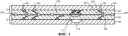
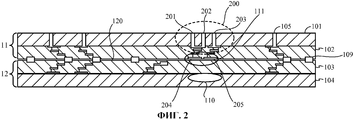
| US12/115,076 US8502373B2 (en) | 2008-05-05 | 2008-05-05 | 3-D integrated circuit lateral heat dissipation |
| US12/115,076 | 2008-05-05 |
Related Parent Applications (1)
| Application Number | Title | Priority Date | Filing Date |
|---|---|---|---|
| RU2010149596/28A Division RU2459315C1 (ru) | 2008-05-05 | 2009-04-27 | Поперечное рассеивание тепла 3-d интегральной схемы |
Publications (2)
| Publication Number | Publication Date |
|---|---|
| RU2012118036A RU2012118036A (ru) | 2013-11-10 |
| RU2502154C1 true RU2502154C1 (ru) | 2013-12-20 |
Family
ID=40941689
Family Applications (2)
| Application Number | Title | Priority Date | Filing Date |
|---|---|---|---|
| RU2012118036/28A RU2502154C1 (ru) | 2008-05-05 | 2009-04-27 | Поперечное рассеивание тепла 3-d интегральной схемы |
| RU2010149596/28A RU2459315C1 (ru) | 2008-05-05 | 2009-04-27 | Поперечное рассеивание тепла 3-d интегральной схемы |
Family Applications After (1)
| Application Number | Title | Priority Date | Filing Date |
|---|---|---|---|
| RU2010149596/28A RU2459315C1 (ru) | 2008-05-05 | 2009-04-27 | Поперечное рассеивание тепла 3-d интегральной схемы |
Country Status (11)
Families Citing this family (24)
| Publication number | Priority date | Publication date | Assignee | Title |
|---|---|---|---|---|
| US8232137B2 (en) * | 2009-12-10 | 2012-07-31 | Intersil Americas Inc. | Heat conduction for chip stacks and 3-D circuits |
| KR20110088234A (ko) * | 2010-01-28 | 2011-08-03 | 삼성전자주식회사 | 적층 반도체 패키지의 제조 방법 |
| US8405203B2 (en) | 2010-09-10 | 2013-03-26 | Cisco Technology, Inc. | Semiconductor package with integrated substrate thermal slug |
| US8193039B2 (en) * | 2010-09-24 | 2012-06-05 | Advanced Micro Devices, Inc. | Semiconductor chip with reinforcing through-silicon-vias |
| US9704793B2 (en) | 2011-01-04 | 2017-07-11 | Napra Co., Ltd. | Substrate for electronic device and electronic device |
| JP5250707B2 (ja) * | 2011-05-26 | 2013-07-31 | 有限会社 ナプラ | 電子機器用基板及び電子機器 |
| US8367478B2 (en) | 2011-06-02 | 2013-02-05 | International Business Machines Corporation | Method and system for internal layer-layer thermal enhancement |
| US8531032B2 (en) | 2011-09-02 | 2013-09-10 | Taiwan Semiconductor Manufacturing Company, Ltd. | Thermally enhanced structure for multi-chip device |
| FR2999017A1 (fr) * | 2012-12-03 | 2014-06-06 | St Microelectronics Sa | Structure integree tridimensionnelle a dissipation thermique amelioree |
| TWI509758B (zh) | 2012-12-26 | 2015-11-21 | Univ Nat Chiao Tung | 三維積體電路 |
| US10403601B2 (en) * | 2016-06-17 | 2019-09-03 | Fairchild Semiconductor Corporation | Semiconductor package and related methods |
| US10256188B2 (en) | 2016-11-26 | 2019-04-09 | Texas Instruments Incorporated | Interconnect via with grown graphitic material |
| US10529641B2 (en) * | 2016-11-26 | 2020-01-07 | Texas Instruments Incorporated | Integrated circuit nanoparticle thermal routing structure over interconnect region |
| US11676880B2 (en) | 2016-11-26 | 2023-06-13 | Texas Instruments Incorporated | High thermal conductivity vias by additive processing |
| US11004680B2 (en) | 2016-11-26 | 2021-05-11 | Texas Instruments Incorporated | Semiconductor device package thermal conduit |
| US10861763B2 (en) | 2016-11-26 | 2020-12-08 | Texas Instruments Incorporated | Thermal routing trench by additive processing |
| US10811334B2 (en) * | 2016-11-26 | 2020-10-20 | Texas Instruments Incorporated | Integrated circuit nanoparticle thermal routing structure in interconnect region |
| US11276667B2 (en) | 2016-12-31 | 2022-03-15 | Intel Corporation | Heat removal between top and bottom die interface |
| US10163864B1 (en) * | 2017-08-16 | 2018-12-25 | Globalfoundries Inc. | Vertically stacked wafers and methods of forming same |
| US10566313B1 (en) | 2018-08-21 | 2020-02-18 | International Business Machines Corporation | Integrated circuit chip carrier with in-plane thermal conductance layer |
| US10643957B2 (en) | 2018-08-27 | 2020-05-05 | Nxp B.V. | Conformal dummy die |
| US10854530B1 (en) | 2019-07-31 | 2020-12-01 | Taiwan Semiconductor Manufacturing Co., Ltd. | Heat dissipation structures |
| US11211364B1 (en) * | 2020-06-24 | 2021-12-28 | Micron Technology, Inc. | Semiconductor device assemblies and systems with improved thermal performance and methods for making the same |
| CN114334854A (zh) | 2020-09-30 | 2022-04-12 | 华为技术有限公司 | 芯片及其制造方法、电子设备 |
Citations (4)
| Publication number | Priority date | Publication date | Assignee | Title |
|---|---|---|---|---|
| US4764804A (en) * | 1986-02-21 | 1988-08-16 | Hitachi, Ltd. | Semiconductor device and process for producing the same |
| US4823234A (en) * | 1985-08-16 | 1989-04-18 | Dai-Ichi Seiko Co., Ltd. | Semiconductor device and its manufacture |
| US6278181B1 (en) * | 1999-06-28 | 2001-08-21 | Advanced Micro Devices, Inc. | Stacked multi-chip modules using C4 interconnect technology having improved thermal management |
| RU2299497C2 (ru) * | 2005-05-06 | 2007-05-20 | Геннадий Андреевич Блинов | Способ изготовления трехмерного многокристального микромодуля |
Family Cites Families (37)
| Publication number | Priority date | Publication date | Assignee | Title |
|---|---|---|---|---|
| US4731701A (en) * | 1987-05-12 | 1988-03-15 | Fairchild Semiconductor Corporation | Integrated circuit package with thermal path layers incorporating staggered thermal vias |
| JPS63293931A (ja) * | 1987-05-27 | 1988-11-30 | Hitachi Ltd | 半導体装置およびその製造方法 |
| US5050039A (en) * | 1990-06-26 | 1991-09-17 | Digital Equipment Corporation | Multiple circuit chip mounting and cooling arrangement |
| US5414299A (en) * | 1993-09-24 | 1995-05-09 | Vlsi Technology, Inc. | Semi-conductor device interconnect package assembly for improved package performance |
| JPH10502493A (ja) * | 1994-07-05 | 1998-03-03 | シーメンス アクチエンゲゼルシヤフト | 三次元回路装置の製造方法 |
| US5532512A (en) | 1994-10-03 | 1996-07-02 | General Electric Company | Direct stacked and flip chip power semiconductor device structures |
| JP2905736B2 (ja) | 1995-12-18 | 1999-06-14 | 株式会社エイ・ティ・アール光電波通信研究所 | 半導体装置 |
| US20020089016A1 (en) | 1998-07-10 | 2002-07-11 | Jean-Pierre Joly | Thin layer semi-conductor structure comprising a heat distribution layer |
| JP2000040382A (ja) | 1998-07-23 | 2000-02-08 | Sony Corp | 不揮発性半導体記憶装置およびそのデータ書き込み方法 |
| US6573538B2 (en) * | 1998-11-12 | 2003-06-03 | International Business Machines Corporation | Semiconductor device with internal heat dissipation |
| KR20000011896U (ko) * | 1998-12-10 | 2000-07-05 | 윤종용 | 반도체 디바이스의 방열을 위한 히트 싱크 구조 |
| TW413874B (en) * | 1999-04-12 | 2000-12-01 | Siliconware Precision Industries Co Ltd | BGA semiconductor package having exposed heat dissipation layer and its manufacturing method |
| US6720662B1 (en) | 1999-11-04 | 2004-04-13 | Rohm Co., Ltd. | Semiconductor device of chip-on-chip structure with a radiation noise shield |
| JP3570672B2 (ja) | 1999-11-04 | 2004-09-29 | ローム株式会社 | 半導体装置 |
| US6337513B1 (en) * | 1999-11-30 | 2002-01-08 | International Business Machines Corporation | Chip packaging system and method using deposited diamond film |
| US6512292B1 (en) * | 2000-09-12 | 2003-01-28 | International Business Machines Corporation | Semiconductor chip structures with embedded thermal conductors and a thermal sink disposed over opposing substrate surfaces |
| US6333557B1 (en) * | 2000-09-12 | 2001-12-25 | International Business Machines Corporation | Semiconductor chip structures with embedded thermal conductors |
| US6507115B2 (en) * | 2000-12-14 | 2003-01-14 | International Business Machines Corporation | Multi-chip integrated circuit module |
| US6519154B1 (en) * | 2001-08-17 | 2003-02-11 | Intel Corporation | Thermal bus design to cool a microelectronic die |
| JP4416376B2 (ja) * | 2002-05-13 | 2010-02-17 | 富士通株式会社 | 半導体装置及びその製造方法 |
| US7138711B2 (en) * | 2002-06-17 | 2006-11-21 | Micron Technology, Inc. | Intrinsic thermal enhancement for FBGA package |
| JP2004200347A (ja) * | 2002-12-18 | 2004-07-15 | Sumitomo Electric Ind Ltd | 高放熱性能を持つ発光ダイオード |
| US6753600B1 (en) * | 2003-01-28 | 2004-06-22 | Thin Film Module, Inc. | Structure of a substrate for a high density semiconductor package |
| US7180745B2 (en) | 2003-10-10 | 2007-02-20 | Delphi Technologies, Inc. | Flip chip heat sink package and method |
| US7205651B2 (en) * | 2004-04-16 | 2007-04-17 | St Assembly Test Services Ltd. | Thermally enhanced stacked die package and fabrication method |
| US20060025515A1 (en) * | 2004-07-27 | 2006-02-02 | Mainstream Engineering Corp. | Nanotube composites and methods for producing |
| CN100377340C (zh) * | 2004-08-11 | 2008-03-26 | 鸿富锦精密工业(深圳)有限公司 | 散热模组及其制备方法 |
| JP2006120976A (ja) * | 2004-10-25 | 2006-05-11 | Matsushita Electric Ind Co Ltd | 半導体装置およびその製造方法 |
| US7416789B2 (en) | 2004-11-01 | 2008-08-26 | H.C. Starck Inc. | Refractory metal substrate with improved thermal conductivity |
| US20060145356A1 (en) | 2005-01-06 | 2006-07-06 | International Business Machines Corporation | On-chip cooling |
| US20070235847A1 (en) * | 2005-09-19 | 2007-10-11 | Shriram Ramanathan | Method of making a substrate having thermally conductive structures and resulting devices |
| US7528494B2 (en) * | 2005-11-03 | 2009-05-05 | International Business Machines Corporation | Accessible chip stack and process of manufacturing thereof |
| US7514116B2 (en) * | 2005-12-30 | 2009-04-07 | Intel Corporation | Horizontal Carbon Nanotubes by Vertical Growth and Rolling |
| JP2007221078A (ja) | 2006-02-20 | 2007-08-30 | Denso Corp | 半導体装置 |
| US7414316B2 (en) | 2006-03-01 | 2008-08-19 | Freescale Semiconductor, Inc. | Methods and apparatus for thermal isolation in vertically-integrated semiconductor devices |
| US7738249B2 (en) * | 2007-10-25 | 2010-06-15 | Endicott Interconnect Technologies, Inc. | Circuitized substrate with internal cooling structure and electrical assembly utilizing same |
| US8497587B2 (en) * | 2009-12-30 | 2013-07-30 | Stmicroelectronics Pte Ltd. | Thermally enhanced expanded wafer level package ball grid array structure and method of making the same |
-
2008
- 2008-05-05 US US12/115,076 patent/US8502373B2/en active Active
-
2009
- 2009-04-27 CN CN201310119417.5A patent/CN103219328B/zh active Active
- 2009-04-27 JP JP2011508547A patent/JP2011520286A/ja active Pending
- 2009-04-27 KR KR1020107027421A patent/KR101255675B1/ko active Active
- 2009-04-27 RU RU2012118036/28A patent/RU2502154C1/ru active
- 2009-04-27 EP EP09743273A patent/EP2286452A1/en not_active Withdrawn
- 2009-04-27 BR BRPI0912376A patent/BRPI0912376A2/pt not_active Application Discontinuation
- 2009-04-27 WO PCT/US2009/041780 patent/WO2009137286A1/en active Application Filing
- 2009-04-27 CN CN2009801152899A patent/CN102017139B/zh active Active
- 2009-04-27 CA CA2720966A patent/CA2720966C/en active Active
- 2009-04-27 MX MX2010011848A patent/MX2010011848A/es active IP Right Grant
- 2009-04-27 RU RU2010149596/28A patent/RU2459315C1/ru active
- 2009-05-05 TW TW098114847A patent/TWI496269B/zh active
-
2012
- 2012-12-26 JP JP2012283703A patent/JP5788379B2/ja active Active
-
2015
- 2015-05-27 JP JP2015107780A patent/JP2015167259A/ja active Pending
Patent Citations (4)
| Publication number | Priority date | Publication date | Assignee | Title |
|---|---|---|---|---|
| US4823234A (en) * | 1985-08-16 | 1989-04-18 | Dai-Ichi Seiko Co., Ltd. | Semiconductor device and its manufacture |
| US4764804A (en) * | 1986-02-21 | 1988-08-16 | Hitachi, Ltd. | Semiconductor device and process for producing the same |
| US6278181B1 (en) * | 1999-06-28 | 2001-08-21 | Advanced Micro Devices, Inc. | Stacked multi-chip modules using C4 interconnect technology having improved thermal management |
| RU2299497C2 (ru) * | 2005-05-06 | 2007-05-20 | Геннадий Андреевич Блинов | Способ изготовления трехмерного многокристального микромодуля |
Also Published As
| Publication number | Publication date |
|---|---|
| US8502373B2 (en) | 2013-08-06 |
| RU2010149596A (ru) | 2012-06-20 |
| JP2011520286A (ja) | 2011-07-14 |
| BRPI0912376A2 (pt) | 2018-02-27 |
| CN103219328B (zh) | 2017-04-12 |
| JP5788379B2 (ja) | 2015-09-30 |
| US20090273068A1 (en) | 2009-11-05 |
| KR20110004475A (ko) | 2011-01-13 |
| RU2459315C1 (ru) | 2012-08-20 |
| KR101255675B1 (ko) | 2013-04-17 |
| RU2012118036A (ru) | 2013-11-10 |
| WO2009137286A1 (en) | 2009-11-12 |
| CA2720966A1 (en) | 2009-11-12 |
| JP2013077837A (ja) | 2013-04-25 |
| JP2015167259A (ja) | 2015-09-24 |
| TW201005917A (en) | 2010-02-01 |
| CN103219328A (zh) | 2013-07-24 |
| MX2010011848A (es) | 2010-11-30 |
| CN102017139B (zh) | 2013-05-08 |
| CA2720966C (en) | 2015-06-30 |
| CN102017139A (zh) | 2011-04-13 |
| TWI496269B (zh) | 2015-08-11 |
| EP2286452A1 (en) | 2011-02-23 |
Similar Documents
| Publication | Publication Date | Title |
|---|---|---|
| RU2502154C1 (ru) | Поперечное рассеивание тепла 3-d интегральной схемы | |
| TWI455278B (zh) | 用於堆疊式積體電路裝置之主動式熱控制 | |
| US7787252B2 (en) | Preferentially cooled electronic device | |
| US10103094B2 (en) | Method and structures for heat dissipating interposers | |
| US9184112B1 (en) | Cooling apparatus for an integrated circuit | |
| TW571415B (en) | Double side connected type semiconductor apparatus | |
| TWI636535B (zh) | 具有嵌埋式熱電裝置之玻璃中介層 | |
| CN112352311A (zh) | 带有芯片内散热器的集成电路 | |
| US7049695B1 (en) | Method and device for heat dissipation in semiconductor modules | |
| CN102569227A (zh) | 集成电路散热系统及制作方法 | |
| US9839159B1 (en) | Dispense pattern for thermal interface material for a high aspect ratio thermal interface | |
| CN102543917B (zh) | 集成电路散热装置 | |
| CN102543917A (zh) | 集成电路散热装置 |