RU2502154C1 - 3-d integrated circuit lateral heat dissipation - Google Patents
3-d integrated circuit lateral heat dissipation Download PDFInfo
- Publication number
- RU2502154C1 RU2502154C1 RU2012118036/28A RU2012118036A RU2502154C1 RU 2502154 C1 RU2502154 C1 RU 2502154C1 RU 2012118036/28 A RU2012118036/28 A RU 2012118036/28A RU 2012118036 A RU2012118036 A RU 2012118036A RU 2502154 C1 RU2502154 C1 RU 2502154C1
- Authority
- RU
- Russia
- Prior art keywords
- heat
- crystal
- crystals
- conducting material
- layers
- Prior art date
Links
Images
Classifications
-
- H—ELECTRICITY
- H01—ELECTRIC ELEMENTS
- H01L—SEMICONDUCTOR DEVICES NOT COVERED BY CLASS H10
- H01L25/00—Assemblies consisting of a plurality of individual semiconductor or other solid state devices ; Multistep manufacturing processes thereof
- H01L25/03—Assemblies consisting of a plurality of individual semiconductor or other solid state devices ; Multistep manufacturing processes thereof all the devices being of a type provided for in the same subgroup of groups H01L27/00 - H01L33/00, or in a single subclass of H10K, H10N, e.g. assemblies of rectifier diodes
- H01L25/04—Assemblies consisting of a plurality of individual semiconductor or other solid state devices ; Multistep manufacturing processes thereof all the devices being of a type provided for in the same subgroup of groups H01L27/00 - H01L33/00, or in a single subclass of H10K, H10N, e.g. assemblies of rectifier diodes the devices not having separate containers
- H01L25/065—Assemblies consisting of a plurality of individual semiconductor or other solid state devices ; Multistep manufacturing processes thereof all the devices being of a type provided for in the same subgroup of groups H01L27/00 - H01L33/00, or in a single subclass of H10K, H10N, e.g. assemblies of rectifier diodes the devices not having separate containers the devices being of a type provided for in group H01L27/00
- H01L25/0657—Stacked arrangements of devices
-
- H—ELECTRICITY
- H01—ELECTRIC ELEMENTS
- H01L—SEMICONDUCTOR DEVICES NOT COVERED BY CLASS H10
- H01L23/00—Details of semiconductor or other solid state devices
- H01L23/34—Arrangements for cooling, heating, ventilating or temperature compensation ; Temperature sensing arrangements
- H01L23/36—Selection of materials, or shaping, to facilitate cooling or heating, e.g. heatsinks
- H01L23/367—Cooling facilitated by shape of device
- H01L23/3677—Wire-like or pin-like cooling fins or heat sinks
-
- H—ELECTRICITY
- H01—ELECTRIC ELEMENTS
- H01L—SEMICONDUCTOR DEVICES NOT COVERED BY CLASS H10
- H01L23/00—Details of semiconductor or other solid state devices
- H01L23/34—Arrangements for cooling, heating, ventilating or temperature compensation ; Temperature sensing arrangements
- H01L23/36—Selection of materials, or shaping, to facilitate cooling or heating, e.g. heatsinks
- H01L23/373—Cooling facilitated by selection of materials for the device or materials for thermal expansion adaptation, e.g. carbon
- H01L23/3732—Diamonds
-
- H—ELECTRICITY
- H01—ELECTRIC ELEMENTS
- H01L—SEMICONDUCTOR DEVICES NOT COVERED BY CLASS H10
- H01L23/00—Details of semiconductor or other solid state devices
- H01L23/34—Arrangements for cooling, heating, ventilating or temperature compensation ; Temperature sensing arrangements
- H01L23/36—Selection of materials, or shaping, to facilitate cooling or heating, e.g. heatsinks
- H01L23/373—Cooling facilitated by selection of materials for the device or materials for thermal expansion adaptation, e.g. carbon
- H01L23/3735—Laminates or multilayers, e.g. direct bond copper ceramic substrates
-
- H—ELECTRICITY
- H01—ELECTRIC ELEMENTS
- H01L—SEMICONDUCTOR DEVICES NOT COVERED BY CLASS H10
- H01L2224/00—Indexing scheme for arrangements for connecting or disconnecting semiconductor or solid-state bodies and methods related thereto as covered by H01L24/00
- H01L2224/01—Means for bonding being attached to, or being formed on, the surface to be connected, e.g. chip-to-package, die-attach, "first-level" interconnects; Manufacturing methods related thereto
- H01L2224/10—Bump connectors; Manufacturing methods related thereto
- H01L2224/15—Structure, shape, material or disposition of the bump connectors after the connecting process
- H01L2224/16—Structure, shape, material or disposition of the bump connectors after the connecting process of an individual bump connector
- H01L2224/161—Disposition
- H01L2224/16135—Disposition the bump connector connecting between different semiconductor or solid-state bodies, i.e. chip-to-chip
- H01L2224/16145—Disposition the bump connector connecting between different semiconductor or solid-state bodies, i.e. chip-to-chip the bodies being stacked
-
- H—ELECTRICITY
- H01—ELECTRIC ELEMENTS
- H01L—SEMICONDUCTOR DEVICES NOT COVERED BY CLASS H10
- H01L2225/00—Details relating to assemblies covered by the group H01L25/00 but not provided for in its subgroups
- H01L2225/03—All the devices being of a type provided for in the same subgroup of groups H01L27/00 - H01L33/648 and H10K99/00
- H01L2225/04—All the devices being of a type provided for in the same subgroup of groups H01L27/00 - H01L33/648 and H10K99/00 the devices not having separate containers
- H01L2225/065—All the devices being of a type provided for in the same subgroup of groups H01L27/00 - H01L33/648 and H10K99/00 the devices not having separate containers the devices being of a type provided for in group H01L27/00
- H01L2225/06503—Stacked arrangements of devices
- H01L2225/06513—Bump or bump-like direct electrical connections between devices, e.g. flip-chip connection, solder bumps
-
- H—ELECTRICITY
- H01—ELECTRIC ELEMENTS
- H01L—SEMICONDUCTOR DEVICES NOT COVERED BY CLASS H10
- H01L2225/00—Details relating to assemblies covered by the group H01L25/00 but not provided for in its subgroups
- H01L2225/03—All the devices being of a type provided for in the same subgroup of groups H01L27/00 - H01L33/648 and H10K99/00
- H01L2225/04—All the devices being of a type provided for in the same subgroup of groups H01L27/00 - H01L33/648 and H10K99/00 the devices not having separate containers
- H01L2225/065—All the devices being of a type provided for in the same subgroup of groups H01L27/00 - H01L33/648 and H10K99/00 the devices not having separate containers the devices being of a type provided for in group H01L27/00
- H01L2225/06503—Stacked arrangements of devices
- H01L2225/06589—Thermal management, e.g. cooling
-
- H—ELECTRICITY
- H01—ELECTRIC ELEMENTS
- H01L—SEMICONDUCTOR DEVICES NOT COVERED BY CLASS H10
- H01L2924/00—Indexing scheme for arrangements or methods for connecting or disconnecting semiconductor or solid-state bodies as covered by H01L24/00
- H01L2924/01—Chemical elements
- H01L2924/01019—Potassium [K]
Abstract
Description
Область техники, к которой относится раскрытие изобретенияFIELD OF THE INVENTION
Данное раскрытие относится к интегральным схемам (ИС), более конкретно к многослойным (3-D) ИС, еще более конкретно к системам и способам для улучшения рассеивания тепла в 3-D ИС.This disclosure relates to integrated circuits (ICs), more specifically to multilayer (3-D) ICs, and more particularly to systems and methods for improving heat dissipation in 3-D ICs.
Уровень техникиState of the art
В технологии ИС существует потребность в укладке чипов (кристаллов) вместе для формирования многослойных или трехмерных (3-D) ИС устройств. Одним из результатов такой 3-D ИС укладки является уменьшение времени прохождения сигнала во время обработки сигналов в связи с уменьшением расстояния, которое сигналы должны пройти, когда они остаются внутри одного блока.In IC technology, there is a need for stacking chips (crystals) together to form multilayer or three-dimensional (3-D) IC devices. One of the results of such a 3-D stacking IC is the reduction of the signal travel time during signal processing due to the reduction in the distance that the signals must travel when they remain inside one unit.
Один способ соединения слоев заключается в соединении двух (или более) кристаллов вместе и последующем заключении кристаллов в единой структуре. Электрические проводники и/или контакты на поверхности соответствующих кристаллов служат для того, чтобы проводить электрические сигналы между компонентами различных кристаллов.One way to connect the layers is to connect two (or more) crystals together and then enclose the crystals in a single structure. Electrical conductors and / or contacts on the surface of the respective crystals serve to conduct electrical signals between the components of various crystals.
Одна из проблем в ситуации, когда кристаллы расположены очень близко друг к другу, заключается в том, что увеличивается интенсивность нагревания. Более того, из-за уменьшенного размера сложенных ИС (с толщиной подложки, от 700-100 микрон до менее чем 20 микрон), поперечная тепловая проводимость уменьшается. Таким образом, могут существовать горячие точки со слабой способностью отводить тепло от источника тепла.One of the problems in a situation where the crystals are located very close to each other is that the heating intensity increases. Moreover, due to the reduced size of the folded ICs (with the thickness of the substrate, from 700-100 microns to less than 20 microns), the transverse thermal conductivity is reduced. Thus, there may be hot spots with poor ability to remove heat from a heat source.
Один способ увеличения поперечной тепловой проводимости заключается в увеличении толщины подложки, по меньшей мере, одного из слоев. Другой способ заключается в увеличении металлических слоев в чипе для того, чтобы сделать возможным рассеивание тепла. Это, в свою очередь отрицательно влияет на соотношение геометрических размеров, а также уменьшает скорости прохождения сигналов.One way to increase the transverse thermal conductivity is to increase the thickness of the substrate of at least one of the layers. Another way is to increase the metal layers in the chip in order to make heat dissipation possible. This, in turn, negatively affects the ratio of geometric dimensions, and also reduces the speed of transmission of signals.
Существует дополнительная проблема при соединении более одного слоя. В таких ситуациях многослойное ИС устройство содержит множество слоев оксида между слоями. Оксид, являясь плохим проводником тепла, усугубляет проблему рассеивания тепла.There is an additional problem when connecting more than one layer. In such situations, a multilayer IC device contains many oxide layers between the layers. Oxide, being a poor conductor of heat, exacerbates the problem of heat dissipation.
Существует несколько подходов, которые можно выбрать для решения проблем проводимости тепла. Один подход предполагает использование сквозных соединений сквозь кремний (TSV), чтобы отводить тепло от внутренней части поверхностного слоя, и затем отводить тепло, используя традиционные способы, такие как размещение материалов с высокой тепловой проводимостью на поверхности корпуса ИС. Проблема при таком решении заключается в том, что топология схемы может не позволить расположить TSV в нужном месте из-за устройств, сконструированных в различных слоях вблизи горячей точки, генерирующей тепло.There are several approaches that you can choose to solve heat conduction problems. One approach involves using end-to-end compounds through silicon (TSV) to remove heat from the inside of the surface layer and then remove heat using traditional methods, such as placing materials with high thermal conductivity on the surface of the IC enclosure. The problem with this solution is that the circuit topology may not allow the TSV to be located in the right place due to devices designed in different layers near the hot spot that generates heat.
Другой способ заключается в циркуляции охлаждающего материала через упакованное ИС устройство для охлаждения различных горячих точек. Это дорого в производстве, так как перемещающаяся жидкость требует накачивающего механизма и жестких допусков для каналов движения жидкости. Также может оказаться невозможным подведение охлаждающего материала к необходимой области. Проблема каналов может быть решена до некоторой степени путем форсирования охлаждающего жидкого материала через саму подложку, но этот способ не лишен определенного набора проблем и затрат.Another method is to circulate cooling material through a packaged IC device for cooling various hot spots. It is expensive to manufacture, since moving fluid requires a pumping mechanism and tight tolerances for fluid flow channels. It may also be impossible to bring the cooling material to the desired area. The channel problem can be solved to some extent by forcing the cooling liquid material through the substrate itself, but this method is not without a certain set of problems and costs.
Раскрытие изобретенияDisclosure of invention
Варианты осуществления изобретения предусматривают заполнение воздушных промежутков между уложенными (упакованными) кристаллами проводящим тепло материалом, что позволяет отводить в поперечном направлении тепло, генерируемое в одной или нескольких областях внутри каждого кристалла. Отвод тепла в поперечном направлении может осуществляться вдоль всей длины кристалла или вдоль части его длины. В одном варианте осуществления тепловой материал является электрически изолирующим. В одном варианте осуществления TSV, возможно, с использованием углеродных нанотрубок, могут быть сконструированы в определенных областях для поддержания рассеивания тепла в проблемных тепловых областях.Embodiments of the invention provide for filling the air gaps between the stacked (packed) crystals with a heat-conducting material, which makes it possible to remove in the transverse direction the heat generated in one or more areas within each crystal. The heat can be removed in the transverse direction along the entire length of the crystal or along part of its length. In one embodiment, the thermal material is electrically insulating. In one embodiment, TSVs, possibly using carbon nanotubes, can be designed in specific areas to maintain heat dissipation in problematic thermal areas.
В одном варианте осуществления многослойный полупроводник имеет проводящий тепло материал, расположенный между первым и вторым слоями, причем материал имеет более высокую тепловую проводимость по сравнению с тепловой проводимостью упомянутых первого и второго слоев.In one embodiment, the multilayer semiconductor has a heat conductive material located between the first and second layers, the material having a higher thermal conductivity compared to the thermal conductivity of said first and second layers.
В другом варианте осуществления раскрыт способ изготовления многослойного полупроводника, в котором проводящий тепло материал используется на, по меньшей мере, одной сопрягаемой поверхности первого кристалла, а сопрягаемая поверхность этого кристалла соединяется с сопрягаемой поверхностью второго кристалла.In another embodiment, a method for manufacturing a multilayer semiconductor is disclosed in which heat-conducting material is used on at least one mating surface of the first crystal, and the mating surface of this crystal is connected to the mating surface of the second crystal.
Еще в одном варианте осуществления раскрыт способ рассеивания тепла в упакованном ИС устройстве, который позволяет отводить тепло из проблемной тепловой области одного слоя многослойного ИС устройства во внутренний слой между смежными слоями устройства таким образом, чтобы содействовать поперечному отводу тепла в области внутреннего слоя до, по меньшей мере, одной области теплового рассеивания, термически связанной с областью внутреннего слоя. В одном варианте осуществления область рассеивания тепла является сквозным соединением, выполненным через, по меньшей мере, один слой кристалла устройства. В другом варианте осуществления область рассеивания тепла является промежутком между соседними кристаллами одного слоя.In yet another embodiment, a method of heat dissipation in a packaged IC device is disclosed, which allows heat to be removed from the problematic thermal region of one layer of the multilayer IC device to the inner layer between adjacent layers of the device so as to facilitate transverse heat removal in the region of the inner layer to at least at least one area of thermal dissipation, thermally associated with the region of the inner layer. In one embodiment, the heat dissipation region is a through connection made through at least one crystal layer of the device. In another embodiment, the heat dissipation region is the gap between adjacent crystals of the same layer.
Приведенное выше описание довольно широко обрисовывает признаки и технические преимущества данного изобретения для того, чтобы подробное описание, приведенное далее, могло быть лучше понято. Далее описаны дополнительные признаки и преимущества, которые формируют заявленный объект формулы изобретения. Специалисты в данной области техники оценят то, что концепция и раскрытые специфические варианты изобретения могут быть легко использованы в качестве основы для модификации или проектирования других структур для выполнения тех же задач данного изобретения. Также специалистам в данной области техники должно быть понятно, что такие аналогичные конструкции не выходят за рамки сущности и объема изобретения в соответствии с тем, что указано далее в приложенной формуле изобретения. Новые признаки, которые считаются характеристикой изобретения, как относительно соответствующей структуры, так и способов работы, вместе с другими целями и преимуществами будут лучше поняты из приведенного далее описания при рассмотрении совместно с приложенными чертежами. Однако должно быть понятно, что каждый из чертежей приведен только с целью иллюстрации и описания и не предназначается для определения объема настоящего изобретения.The above description describes the features and technical advantages of the present invention quite broadly so that the detailed description given below can be better understood. The following describes additional features and advantages that form the claimed subject matter of the claims. Those skilled in the art will appreciate that the concept and specific embodiments of the invention disclosed can easily be used as the basis for modifying or designing other structures to accomplish the same objectives of the present invention. Also, specialists in the art should understand that such similar designs do not go beyond the essence and scope of the invention in accordance with what is indicated below in the attached claims. New features that are considered a characteristic of the invention, both with respect to the corresponding structure and methods of operation, together with other objectives and advantages will be better understood from the following description when considered in conjunction with the attached drawings. However, it should be understood that each of the drawings is provided for purposes of illustration and description only and is not intended to determine the scope of the present invention.
Краткое описание чертежейBrief Description of the Drawings
Для более полного понимания данного раскрытия изобретения, далее приведены ссылки на последующее описания совместно с приложенными чертежами.For a more complete understanding of this disclosure, the following are links to the following descriptions in conjunction with the attached drawings.
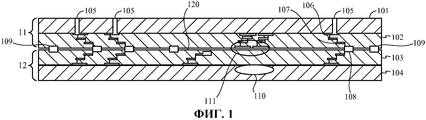
Фиг.1 является видом сбоку в поперечном сечении, изображающим один аспект проблемных тепловых условий, которые могут существовать в 3-D интегральных схемах.Figure 1 is a cross-sectional side view depicting one aspect of problematic thermal conditions that may exist in 3-D integrated circuits.
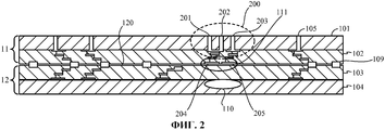
Фиг.2 является видом сбоку в поперечном разрезе, изображающим одно примерное решение проблемы отвода тепла.2 is a cross-sectional side view showing one exemplary solution to a heat dissipation problem.
Фиг.3 является видом сбоку в поперечном разрезе, изображающим один вариант осуществления концепций раскрытия изобретения.FIG. 3 is a cross-sectional side view showing one embodiment of the disclosure concepts.
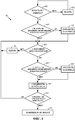
Фиг.4 изображает один вариант осуществления способа конструирования многослойного ИС устройства в соответствии с описанием настоящего раскрытия изобретения.4 depicts one embodiment of a method for constructing a multilayer IC device in accordance with the description of the present disclosure.
Осуществление изобретенияThe implementation of the invention
Фиг.1 изображает один аспект условий проблемы нагрева, которая может существовать в 3-D интегральных схемах. Как изображено на Фиг.1, кристалл 11 сложен с кристаллом 12. Активным слоем кристалла 11 является слой 102, а активным слоем кристалла 12 является слой 103. Это примерное расположение активных слоев кристаллов может иметь любую ориентацию, вверх или вниз.Figure 1 depicts one aspect of the conditions of a heating problem that may exist in 3-D integrated circuits. As shown in FIG. 1, the
Сквозные соединения 105 проходят через слой подложки 101 кристалла 11. Сквозные соединения могут быть выполнены в слоях 102, 103 и/или 104 по желанию. Электрические дорожки 107 и 108 формируют соединение между кристаллами. Уплотнение 109 предотвращает попадание нежелательных загрязнений в область 120 между соответствующими кристаллами 11, 12.Through
Элемент 108 обычно порядка 30 микрон или меньше и обычно принимает вид соединения между металлами из меди или олова и меди. Область 120 обычно является воздушным промежутком. Промежуток 120 может быть в интервале менее 10 микрон.
Горячая точка 110 находится на кристалле 12, и задача заключается в отводе тепла от этой относительно небольшой области 110 к остальной части блока кристаллов. Отметим, что элементы 111 находятся непосредственно над горячей точкой 110, и на них будет воздействовать тепло от горячей точки 110, проходящее вверх через слои 103, 102, 101.The
Фиг.2 изображает одно описываемое решение проблемы отвода тепла. В этом решении множество TSV 200, имеющее отдельные TSV 201, 202 и 203 помещено, чтобы обеспечить проводимость тепла для тепла от горячей точки 110. Тепло проходит через слой 103, который является активной областью нижнего кристалла 12. Тепло затем проходит через активный слой 102 кристалла 11, и затем оно отводится наружу через множество TSV 200. Сквозные соединения 201, 202, 203 могут быть покрыты медью или вольфрамом для увеличения проводимости тепла, но мог бы использоваться любой из проводящих тепло материалов. В одном варианте осуществления могут быть использованы углеродные нанотрубки (УНТ) для заполнения сквозных соединений 201, 202, 203. В другом варианте осуществления УНТ частично заполняют сквозные соединения 201, 202, 203, а металл заполняет оставшееся пространство сквозных соединений 201, 202, 203. Преимуществом УНТ является увеличенная электрическая и тепловая проводимость, а также увеличенная плотность тока.Figure 2 depicts one described solution to the problem of heat dissipation. In this solution, a plurality of
Фиг.3 изображает один вариант осуществления 30, в котором использованы концепции раскрытия изобретения. Проводящий тепло материал 320 расположен внутри промежутка между кристаллами 31 и 32. В другом варианте осуществления проводящий тепло материал 320 расположен между металлическими слоями (не изображены) одного из активных слоев 302, 303 кристаллов 31, 32. Проводящий тепло материал 320 в идеале будет иметь тепловую проводимость, равную более чем 10 Вт/м/К, чтобы способствовать поперечному переносу тепла. Материал 320 является проводящим тепло и в одном варианте осуществления электрически изолирующим, так что он не закорачивает электрические соединения, которые соединяют кристаллы 31, 32, что помешало бы работе элементов, содержащихся в кристаллах 31, 32. Материал 320 может быть расположен множеством способов, например, эжектированием или осаждением путем химического осаждения из газовой фазы (ХОГФ) и/или физического осаждения из газовой фазы (ФОГФ). Материал 320 может являться алмазной матрицей или алмазной пленочной структурой.FIG. 3 depicts one embodiment 30 that utilizes the concepts of the disclosure. Heat conductive material 320 is located inside the gap between crystals 31 and 32. In another embodiment, heat conductive material 320 is located between the metal layers (not shown) of one of the active layers 302, 303 of crystals 31, 32. Heat conductive material 320 ideally will have thermal conductivity of more than 10 W / m / K to facilitate transverse heat transfer. The material 320 is heat conductive and, in one embodiment, electrically insulating, so that it does not short-circuit the electrical connections that connect the crystals 31, 32, which would interfere with the operation of the elements contained in the crystals 31, 32. The material 320 can be arranged in many ways, for example , by ejection or deposition by chemical vapor deposition (CVD) and / or physical vapor deposition (CVD). Material 320 may be a diamond matrix or diamond film structure.
Хотя он изображен только на одном слое 302 одного из кристаллов 31, материал 320 может быть помещен на поверхность каждого из двух сопрягаемых слоев 302, 303, так, что материал 320 на каждом из слоев 302, 303 фактически касается один другого при укладке кристаллов 31, 32. Как вариант, материал 320 может быть помещен только на один из сопрягаемых слоев 302, 303.Although it is depicted on only one layer 302 of one of the crystals 31, material 320 can be placed on the surface of each of the two mating layers 302, 303, so that the material 320 on each of the layers 302, 303 actually touches each other when laying crystals 31, 32. Alternatively, material 320 can only be placed on one of the mating layers 302, 303.
В процессе работы тепло от горячей точки 310 проходит вверх через слой 303 кристалла 32 и в материал 320. Тепло затем распространяется поперечно вдоль материала 320 как к краю устройства, такому, как нависающий край 330, так и, что более типично, тепло пройдет вверх через одно или более рассеивающих сквозных соединений, таких как сквозное соединение 331, выполненное в слое 301 кристалла 31. Из-за поперечного распространения тепла температура распределяется более равномерно вдоль устройства 30. Это преимущество позволяет теплу распространяться относительно быстро вдоль всего устройства 30, тем самым заставляя устройство 30 нагреваться равномерно. Отвод тепла от большей области, такой, как все устройство 30 или корпуса устройства легче осуществить, чем отвод тепла от маленькой внутренней области.During operation, heat from the hot spot 310 passes upward through the layer 303 of the crystal 32 and into the material 320. Heat then spreads transversely along the material 320 to both the edge of the device, such as the overhanging edge 330, and, more typically, the heat will pass upward through one or more dissipative through-joints, such as through-through 331 made in the layer 301 of the crystal 31. Due to the transverse distribution of heat, the temperature is distributed more evenly along the device 30. This advantage allows the heat to spread. no fast along the entire device 30, thereby causing the device 30 is heated uniformly. Heat can be removed from a larger area, such as the entire device 30 or device case, more easily than heat can be removed from a small internal area.
Отметим, что рассеивающее тепло сквозное соединение 331 может проходить вверх через кристалл 31 или вниз через кристалл 32 (или через оба). Одним преимуществом проводящего тепло материала 320 является то, что рассеивающее тепло сквозное соединение 331 может быть смещено от проблемной тепловой области 310, тем самым освобождая области непосредственно над проблемной областью для использования электрической схемы или других элементов, сконструированных в различных слоях 301, 302, 303. Также отметим, что тепло не должно проходить непосредственно вверх через слои 301, 302, 303, а, предпочтительно сквозное соединение 331 может, например, быть расположено под углом и/или быть изогнутым. Другое преимущество поперечного рассеивания тепла заключается в том, что нужно меньшее количество TSV.Note that the heat dissipating through-joint 331 can pass up through the crystal 31 or down through the crystal 32 (or both). One advantage of the heat-conducting material 320 is that the heat-dissipating through-joint 331 can be offset from the problematic thermal region 310, thereby freeing areas directly above the problematic region to use electrical circuits or other elements constructed in different layers 301, 302, 303. Also note that the heat should not pass directly upward through the layers 301, 302, 303, but preferably the through connection 331 may, for example, be angled and / or curved. Another advantage of lateral heat dissipation is that less TSV is needed.
Для многослойных устройств, имеющих более двух слоев, может быть использовано множество межслойных структур рассеивающих тепло материалов. Таким образом, тепло может распространяться в поперечном направлении от источника тепла на первое расстояние внутри первой межслойной области и затем проходить вверх в следующий слой благодаря сквозному соединению, и затем снова распространяться в поперечном направлении (в любую сторону) во второй межслойной области, при условии, что проводящий тепло материал расположен как в первой, так и во второй межслойных областях.For multilayer devices having more than two layers, many interlayer structures of heat-scattering materials can be used. Thus, heat can propagate in the transverse direction from the heat source to a first distance within the first interlayer region and then pass upward into the next layer due to the through connection, and then again propagate in the transverse direction (in either direction) in the second interlayer region, provided that that the heat-conducting material is located in both the first and second interlayer regions.
Одна система, позволяющая осуществлять даже лучший отвод тепла от материала 320, заключается в том, чтобы сделать один из слоев, например кристалл 31, периферически большим, чем другой кристалл 32, тем самым создавая площадь поверхности, такую как площадь поверхности 330, расположенную на нависающем выступе на большем из кристаллов. Отметим, что эта же технология будет работать для нескольких слоев, которые, при желании, можно расположить в виде перемежающихся выступов в зависимости от диаметра. Состав материала 320 не обязательно должен быть однородным на протяжении всей поверхности, а различия в материале 320 можно использовать для улучшения проводимости тепла от горячей(их) точки(ек) 310.One system that allows even better heat removal from the material 320 is to make one of the layers, for example a crystal 31, peripherally larger than the other crystal 32, thereby creating a surface area, such as surface area 330, located on the overhang ledge on the larger of the crystals. Note that the same technology will work for several layers, which, if desired, can be arranged in the form of alternating protrusions depending on the diameter. The composition of the material 320 does not have to be uniform over the entire surface, and differences in the material 320 can be used to improve heat conductivity from the hot spot (s) 310.
В одном варианте осуществления нижний кристалл больше верхнего кристалла. Таким образом, промежуток будет существовать между двумя верхними кристаллами (из одного слоя), которые лежат на нижнем кристалле. В соответствии с данным раскрытием изобретения материал, заполняющий промежуток, может быть обеспечен внутри этого промежутка между верхними кристаллами. Материал, заполняющий промежуток, может являться материалом, проводящим тепло, и может являться любым материалом с хорошей тепловой проводимостью, таким как алмазная пленка. В одном варианте осуществления проводящий температуру материал, заполняющий промежуток, термически соединен с материалом 320 для улучшения передачи тепла из многослойного ИС устройства.In one embodiment, the lower crystal is larger than the upper crystal. Thus, a gap will exist between the two upper crystals (from one layer) that lie on the lower crystal. In accordance with this disclosure of the invention, the material filling the gap can be provided inside this gap between the upper crystals. The material filling the gap may be a material that conducts heat, and may be any material with good thermal conductivity, such as a diamond film. In one embodiment, the temperature conducting material filling the gap is thermally coupled to material 320 to improve heat transfer from the multilayer IC device.
Фиг.4 изображает один вариант осуществления 40 способа конструирования упакованных ИС устройств в соответствии с заявленным изобретением. Процесс 401 определяет, был ли выбран кристалл для конструирования многослойного ИС устройства. Если нет, то процесс 402 контролирует время ожидания. После того, как кристалл выбран, процесс 403 определяет, нужно ли добавлять проводящий тепло материал к, по меньшей мере, одной поверхности кристалла. Проводящий тепло материал может быть осажден под управлением процесса 404 одним из способов, описанных выше, таких как обработка ХОГФ или ФОГФ, или материал может быть эжектирован или осажден в виде пленки.FIG. 4 shows one
Процессы 405 и 406 ожидают выбора следующего кристалла для соединения с ранее выбранным кристаллом. Процессы 407 и 408 добавляют проводящий тепло материал к следующему кристаллу, если необходимо, и процесс 409 затем соединяет кристаллы вместе. Процесс 410 определяет, нужно ли еще добавлять кристаллы. Если все кристаллы выбраны и покрыты проводящим тепло материалом (если необходимо), процесс 411 завершает соединение ИС, которая потом готова к проверке и/или использованию.
Хотя настоящее изобретение и его преимущества были подробно описаны, следует понимать, что различные изменения, замены и альтернативы могут быть осуществлены без отклонения от сущности и объема изобретения, определенных в приложенной формуле изобретения. Например, хотя материал 320 был описан как неэлектропроводный, можно сделать материал электропроводным. В этом варианте осуществления электропроводный материал должен быть структурированным, т.е. чтобы имелась возможность его структурирования таким образом, чтобы он мог быть отделен от некоторых сквозных соединений, чтобы предотвратить электрические соединения, при этом все еще термически рассеивая тепло.Although the present invention and its advantages have been described in detail, it should be understood that various changes, substitutions and alternatives can be made without deviating from the essence and scope of the invention defined in the attached claims. For example, although material 320 has been described as non-conductive, it is possible to make the material conductive. In this embodiment, the electrically conductive material should be structured, i.e. so that it can be structured in such a way that it can be separated from some through connections to prevent electrical connections, while still thermally dissipating heat.
Объем настоящей заявки не предполагается быть ограниченным определенными вариантами осуществления процесса, механизма, производства, состава материала, средств, способов и этапов, описанных в спецификации. Специалисту в данной области техники из настоящего раскрытия будет понятно, что процессы, механизмы, производство, составы материала, средства, способы или этапы, существующие на данный момент или те, которые будут позже разработаны, которые осуществляют практически ту же функцию или обеспечивают практически тот же результат, что и соответствующие раскрытые варианты осуществления, могут быть использованы в соответствии с данным изобретением. Соответственно, приложенная формула изобретения предполагает включение в ее объем таких процессов, механизмов, производства, составов материала, средств, способов или этапов.The scope of this application is not intended to be limited to certain embodiments of the process, mechanism, production, composition of the material, means, methods and steps described in the specification. It will be clear to a person skilled in the art from the present disclosure that processes, mechanisms, production, material compositions, means, methods or steps that currently exist or those that will be later developed, that perform almost the same function or provide almost the same the result, as well as the corresponding disclosed embodiments, can be used in accordance with this invention. Accordingly, the appended claims involve the inclusion in its scope of such processes, mechanisms, production, compositions of the material, means, methods or steps.
Claims (7)
обеспечение сквозного отверстия через подложку, заполненного первым проводящим тепло материалом, расположенного в первом кристалле;
нанесение проводящего тепло слоя на поверхность второго кристалла; и
обеспечение физического межсоединения между вторым кристаллом и сквозным отверстием через подложку посредством проводящего тепло слоя.1. The method of heat dissipation in a three-dimensional device integrated circuit (IC) containing the first crystal, laid with the formation of a layered structure on the second crystal, each of the crystals having constructed elements in it, and the crystals are connected to each other by many interlayer compounds, and interlayer connections create a gap between the first and second crystals, while said method comprises:
providing a through hole through a substrate filled with a first heat-conducting material located in the first crystal;
applying a heat-conducting layer to the surface of the second crystal; and
providing a physical interconnect between the second crystal and the through hole through the substrate by means of a heat-conducting layer.
Applications Claiming Priority (2)
| Application Number | Priority Date | Filing Date | Title |
|---|---|---|---|
| US12/115,076 | 2008-05-05 | ||
| US12/115,076 US8502373B2 (en) | 2008-05-05 | 2008-05-05 | 3-D integrated circuit lateral heat dissipation |
Related Parent Applications (1)
| Application Number | Title | Priority Date | Filing Date |
|---|---|---|---|
| RU2010149596/28A Division RU2459315C1 (en) | 2008-05-05 | 2009-04-27 | 3-d integrated circuit lateral heat dissipation |
Publications (2)
| Publication Number | Publication Date |
|---|---|
| RU2012118036A RU2012118036A (en) | 2013-11-10 |
| RU2502154C1 true RU2502154C1 (en) | 2013-12-20 |
Family
ID=40941689
Family Applications (2)
| Application Number | Title | Priority Date | Filing Date |
|---|---|---|---|
| RU2010149596/28A RU2459315C1 (en) | 2008-05-05 | 2009-04-27 | 3-d integrated circuit lateral heat dissipation |
| RU2012118036/28A RU2502154C1 (en) | 2008-05-05 | 2009-04-27 | 3-d integrated circuit lateral heat dissipation |
Family Applications Before (1)
| Application Number | Title | Priority Date | Filing Date |
|---|---|---|---|
| RU2010149596/28A RU2459315C1 (en) | 2008-05-05 | 2009-04-27 | 3-d integrated circuit lateral heat dissipation |
Country Status (11)
| Country | Link |
|---|---|
| US (1) | US8502373B2 (en) |
| EP (1) | EP2286452A1 (en) |
| JP (3) | JP2011520286A (en) |
| KR (1) | KR101255675B1 (en) |
| CN (2) | CN103219328B (en) |
| BR (1) | BRPI0912376A2 (en) |
| CA (1) | CA2720966C (en) |
| MX (1) | MX2010011848A (en) |
| RU (2) | RU2459315C1 (en) |
| TW (1) | TWI496269B (en) |
| WO (1) | WO2009137286A1 (en) |
Families Citing this family (23)
| Publication number | Priority date | Publication date | Assignee | Title |
|---|---|---|---|---|
| US8232137B2 (en) * | 2009-12-10 | 2012-07-31 | Intersil Americas Inc. | Heat conduction for chip stacks and 3-D circuits |
| KR20110088234A (en) * | 2010-01-28 | 2011-08-03 | 삼성전자주식회사 | Method for fabricating of stacked semiconductor package |
| US8405203B2 (en) | 2010-09-10 | 2013-03-26 | Cisco Technology, Inc. | Semiconductor package with integrated substrate thermal slug |
| US8193039B2 (en) * | 2010-09-24 | 2012-06-05 | Advanced Micro Devices, Inc. | Semiconductor chip with reinforcing through-silicon-vias |
| US9704793B2 (en) | 2011-01-04 | 2017-07-11 | Napra Co., Ltd. | Substrate for electronic device and electronic device |
| JP5250707B2 (en) * | 2011-05-26 | 2013-07-31 | 有限会社 ナプラ | Electronic equipment substrate and electronic equipment |
| US8367478B2 (en) | 2011-06-02 | 2013-02-05 | International Business Machines Corporation | Method and system for internal layer-layer thermal enhancement |
| US8531032B2 (en) | 2011-09-02 | 2013-09-10 | Taiwan Semiconductor Manufacturing Company, Ltd. | Thermally enhanced structure for multi-chip device |
| FR2999017A1 (en) * | 2012-12-03 | 2014-06-06 | St Microelectronics Sa | Three-dimensional integrated structure, useful in telephony applications, comprises chips including substrate and interconnection block that comprises thermally conductive and electrically insulating layer |
| TWI509758B (en) | 2012-12-26 | 2015-11-21 | Univ Nat Chiao Tung | Three-dimesional integrated circuit |
| US10403601B2 (en) * | 2016-06-17 | 2019-09-03 | Fairchild Semiconductor Corporation | Semiconductor package and related methods |
| US10861763B2 (en) | 2016-11-26 | 2020-12-08 | Texas Instruments Incorporated | Thermal routing trench by additive processing |
| US11676880B2 (en) | 2016-11-26 | 2023-06-13 | Texas Instruments Incorporated | High thermal conductivity vias by additive processing |
| US11004680B2 (en) | 2016-11-26 | 2021-05-11 | Texas Instruments Incorporated | Semiconductor device package thermal conduit |
| US10811334B2 (en) * | 2016-11-26 | 2020-10-20 | Texas Instruments Incorporated | Integrated circuit nanoparticle thermal routing structure in interconnect region |
| US10529641B2 (en) * | 2016-11-26 | 2020-01-07 | Texas Instruments Incorporated | Integrated circuit nanoparticle thermal routing structure over interconnect region |
| US10256188B2 (en) | 2016-11-26 | 2019-04-09 | Texas Instruments Incorporated | Interconnect via with grown graphitic material |
| US11276667B2 (en) * | 2016-12-31 | 2022-03-15 | Intel Corporation | Heat removal between top and bottom die interface |
| US10163864B1 (en) * | 2017-08-16 | 2018-12-25 | Globalfoundries Inc. | Vertically stacked wafers and methods of forming same |
| US10566313B1 (en) | 2018-08-21 | 2020-02-18 | International Business Machines Corporation | Integrated circuit chip carrier with in-plane thermal conductance layer |
| US10643957B2 (en) | 2018-08-27 | 2020-05-05 | Nxp B.V. | Conformal dummy die |
| US10854530B1 (en) * | 2019-07-31 | 2020-12-01 | Taiwan Semiconductor Manufacturing Co., Ltd. | Heat dissipation structures |
| CN114334854A (en) * | 2020-09-30 | 2022-04-12 | 华为技术有限公司 | Chip, manufacturing method thereof and electronic device |
Citations (4)
| Publication number | Priority date | Publication date | Assignee | Title |
|---|---|---|---|---|
| US4764804A (en) * | 1986-02-21 | 1988-08-16 | Hitachi, Ltd. | Semiconductor device and process for producing the same |
| US4823234A (en) * | 1985-08-16 | 1989-04-18 | Dai-Ichi Seiko Co., Ltd. | Semiconductor device and its manufacture |
| US6278181B1 (en) * | 1999-06-28 | 2001-08-21 | Advanced Micro Devices, Inc. | Stacked multi-chip modules using C4 interconnect technology having improved thermal management |
| RU2299497C2 (en) * | 2005-05-06 | 2007-05-20 | Геннадий Андреевич Блинов | Method for producing three-dimensional multichip micromodule |
Family Cites Families (37)
| Publication number | Priority date | Publication date | Assignee | Title |
|---|---|---|---|---|
| US4731701A (en) * | 1987-05-12 | 1988-03-15 | Fairchild Semiconductor Corporation | Integrated circuit package with thermal path layers incorporating staggered thermal vias |
| JPS63293931A (en) * | 1987-05-27 | 1988-11-30 | Hitachi Ltd | Semiconductor device and manufacture thereof |
| US5050039A (en) * | 1990-06-26 | 1991-09-17 | Digital Equipment Corporation | Multiple circuit chip mounting and cooling arrangement |
| US5414299A (en) * | 1993-09-24 | 1995-05-09 | Vlsi Technology, Inc. | Semi-conductor device interconnect package assembly for improved package performance |
| WO1996001497A1 (en) * | 1994-07-05 | 1996-01-18 | Siemens Aktiengesellschaft | Method of manufacturing three-dimensional circuits |
| US5532512A (en) * | 1994-10-03 | 1996-07-02 | General Electric Company | Direct stacked and flip chip power semiconductor device structures |
| JP2905736B2 (en) * | 1995-12-18 | 1999-06-14 | 株式会社エイ・ティ・アール光電波通信研究所 | Semiconductor device |
| US20020089016A1 (en) * | 1998-07-10 | 2002-07-11 | Jean-Pierre Joly | Thin layer semi-conductor structure comprising a heat distribution layer |
| JP2000040382A (en) | 1998-07-23 | 2000-02-08 | Sony Corp | Non-volatile semiconductor memory device and data write method thereof |
| US6573538B2 (en) * | 1998-11-12 | 2003-06-03 | International Business Machines Corporation | Semiconductor device with internal heat dissipation |
| KR20000011896U (en) * | 1998-12-10 | 2000-07-05 | 윤종용 | Heat sink structure for heat dissipation of semiconductor devices |
| TW413874B (en) * | 1999-04-12 | 2000-12-01 | Siliconware Precision Industries Co Ltd | BGA semiconductor package having exposed heat dissipation layer and its manufacturing method |
| US6720662B1 (en) * | 1999-11-04 | 2004-04-13 | Rohm Co., Ltd. | Semiconductor device of chip-on-chip structure with a radiation noise shield |
| JP3570672B2 (en) | 1999-11-04 | 2004-09-29 | ローム株式会社 | Semiconductor device |
| US6337513B1 (en) * | 1999-11-30 | 2002-01-08 | International Business Machines Corporation | Chip packaging system and method using deposited diamond film |
| US6512292B1 (en) * | 2000-09-12 | 2003-01-28 | International Business Machines Corporation | Semiconductor chip structures with embedded thermal conductors and a thermal sink disposed over opposing substrate surfaces |
| US6333557B1 (en) * | 2000-09-12 | 2001-12-25 | International Business Machines Corporation | Semiconductor chip structures with embedded thermal conductors |
| US6507115B2 (en) * | 2000-12-14 | 2003-01-14 | International Business Machines Corporation | Multi-chip integrated circuit module |
| US6519154B1 (en) * | 2001-08-17 | 2003-02-11 | Intel Corporation | Thermal bus design to cool a microelectronic die |
| JP4416376B2 (en) * | 2002-05-13 | 2010-02-17 | 富士通株式会社 | Semiconductor device and manufacturing method thereof |
| US7138711B2 (en) * | 2002-06-17 | 2006-11-21 | Micron Technology, Inc. | Intrinsic thermal enhancement for FBGA package |
| JP2004200347A (en) * | 2002-12-18 | 2004-07-15 | Sumitomo Electric Ind Ltd | Light emitting diode with high heat dissipation capability |
| US6753600B1 (en) * | 2003-01-28 | 2004-06-22 | Thin Film Module, Inc. | Structure of a substrate for a high density semiconductor package |
| US7180745B2 (en) * | 2003-10-10 | 2007-02-20 | Delphi Technologies, Inc. | Flip chip heat sink package and method |
| US7205651B2 (en) * | 2004-04-16 | 2007-04-17 | St Assembly Test Services Ltd. | Thermally enhanced stacked die package and fabrication method |
| US20060025515A1 (en) * | 2004-07-27 | 2006-02-02 | Mainstream Engineering Corp. | Nanotube composites and methods for producing |
| CN100377340C (en) * | 2004-08-11 | 2008-03-26 | 鸿富锦精密工业(深圳)有限公司 | Thermal module and manufacturing method thereof |
| JP2006120976A (en) * | 2004-10-25 | 2006-05-11 | Matsushita Electric Ind Co Ltd | Semiconductor device and its manufacturing method |
| US7416789B2 (en) * | 2004-11-01 | 2008-08-26 | H.C. Starck Inc. | Refractory metal substrate with improved thermal conductivity |
| US20060145356A1 (en) * | 2005-01-06 | 2006-07-06 | International Business Machines Corporation | On-chip cooling |
| US20070235847A1 (en) * | 2005-09-19 | 2007-10-11 | Shriram Ramanathan | Method of making a substrate having thermally conductive structures and resulting devices |
| US7528494B2 (en) * | 2005-11-03 | 2009-05-05 | International Business Machines Corporation | Accessible chip stack and process of manufacturing thereof |
| US7514116B2 (en) * | 2005-12-30 | 2009-04-07 | Intel Corporation | Horizontal Carbon Nanotubes by Vertical Growth and Rolling |
| JP2007221078A (en) | 2006-02-20 | 2007-08-30 | Denso Corp | Semiconductor device |
| US7414316B2 (en) * | 2006-03-01 | 2008-08-19 | Freescale Semiconductor, Inc. | Methods and apparatus for thermal isolation in vertically-integrated semiconductor devices |
| US7738249B2 (en) * | 2007-10-25 | 2010-06-15 | Endicott Interconnect Technologies, Inc. | Circuitized substrate with internal cooling structure and electrical assembly utilizing same |
| US8497587B2 (en) * | 2009-12-30 | 2013-07-30 | Stmicroelectronics Pte Ltd. | Thermally enhanced expanded wafer level package ball grid array structure and method of making the same |
-
2008
- 2008-05-05 US US12/115,076 patent/US8502373B2/en active Active
-
2009
- 2009-04-27 WO PCT/US2009/041780 patent/WO2009137286A1/en active Application Filing
- 2009-04-27 CN CN201310119417.5A patent/CN103219328B/en active Active
- 2009-04-27 MX MX2010011848A patent/MX2010011848A/en active IP Right Grant
- 2009-04-27 CN CN2009801152899A patent/CN102017139B/en active Active
- 2009-04-27 JP JP2011508547A patent/JP2011520286A/en active Pending
- 2009-04-27 KR KR1020107027421A patent/KR101255675B1/en active IP Right Grant
- 2009-04-27 CA CA2720966A patent/CA2720966C/en active Active
- 2009-04-27 RU RU2010149596/28A patent/RU2459315C1/en active
- 2009-04-27 RU RU2012118036/28A patent/RU2502154C1/en active
- 2009-04-27 EP EP09743273A patent/EP2286452A1/en not_active Withdrawn
- 2009-04-27 BR BRPI0912376A patent/BRPI0912376A2/en not_active Application Discontinuation
- 2009-05-05 TW TW098114847A patent/TWI496269B/en active
-
2012
- 2012-12-26 JP JP2012283703A patent/JP5788379B2/en active Active
-
2015
- 2015-05-27 JP JP2015107780A patent/JP2015167259A/en active Pending
Patent Citations (4)
| Publication number | Priority date | Publication date | Assignee | Title |
|---|---|---|---|---|
| US4823234A (en) * | 1985-08-16 | 1989-04-18 | Dai-Ichi Seiko Co., Ltd. | Semiconductor device and its manufacture |
| US4764804A (en) * | 1986-02-21 | 1988-08-16 | Hitachi, Ltd. | Semiconductor device and process for producing the same |
| US6278181B1 (en) * | 1999-06-28 | 2001-08-21 | Advanced Micro Devices, Inc. | Stacked multi-chip modules using C4 interconnect technology having improved thermal management |
| RU2299497C2 (en) * | 2005-05-06 | 2007-05-20 | Геннадий Андреевич Блинов | Method for producing three-dimensional multichip micromodule |
Also Published As
| Publication number | Publication date |
|---|---|
| RU2010149596A (en) | 2012-06-20 |
| JP2015167259A (en) | 2015-09-24 |
| CA2720966A1 (en) | 2009-11-12 |
| BRPI0912376A2 (en) | 2018-02-27 |
| RU2459315C1 (en) | 2012-08-20 |
| EP2286452A1 (en) | 2011-02-23 |
| CN103219328B (en) | 2017-04-12 |
| RU2012118036A (en) | 2013-11-10 |
| JP2013077837A (en) | 2013-04-25 |
| TWI496269B (en) | 2015-08-11 |
| JP5788379B2 (en) | 2015-09-30 |
| US8502373B2 (en) | 2013-08-06 |
| JP2011520286A (en) | 2011-07-14 |
| TW201005917A (en) | 2010-02-01 |
| CA2720966C (en) | 2015-06-30 |
| KR20110004475A (en) | 2011-01-13 |
| WO2009137286A1 (en) | 2009-11-12 |
| CN102017139A (en) | 2011-04-13 |
| MX2010011848A (en) | 2010-11-30 |
| KR101255675B1 (en) | 2013-04-17 |
| US20090273068A1 (en) | 2009-11-05 |
| CN102017139B (en) | 2013-05-08 |
| CN103219328A (en) | 2013-07-24 |
Similar Documents
| Publication | Publication Date | Title |
|---|---|---|
| RU2502154C1 (en) | 3-d integrated circuit lateral heat dissipation | |
| TWI455278B (en) | Active thermal control for stacked ic devices | |
| CN104716109B (en) | With packaging part of thermal management component for reducing hot crosstalk and forming method thereof | |
| US7787252B2 (en) | Preferentially cooled electronic device | |
| US7049695B1 (en) | Method and device for heat dissipation in semiconductor modules | |
| US10103094B2 (en) | Method and structures for heat dissipating interposers | |
| US9184112B1 (en) | Cooling apparatus for an integrated circuit | |
| TW571415B (en) | Double side connected type semiconductor apparatus | |
| TWI636535B (en) | Glass interposer with embedded thermoelectric devices | |
| CN102569227B (en) | Integrated circuit radiating system and manufacturing method thereof | |
| US9839159B1 (en) | Dispense pattern for thermal interface material for a high aspect ratio thermal interface | |
| JPH01295455A (en) | Semiconductor laminated and integrated circuit element | |
| CN102543917B (en) | Integrated circuit heat dissipation device | |
| CN102543917A (en) | Cooling device of integrated circuit |