KR20200065074A - 발광 디바이스 패키지 - Google Patents
발광 디바이스 패키지 Download PDFInfo
- Publication number
- KR20200065074A KR20200065074A KR1020207014163A KR20207014163A KR20200065074A KR 20200065074 A KR20200065074 A KR 20200065074A KR 1020207014163 A KR1020207014163 A KR 1020207014163A KR 20207014163 A KR20207014163 A KR 20207014163A KR 20200065074 A KR20200065074 A KR 20200065074A
- Authority
- KR
- South Korea
- Prior art keywords
- coating layer
- base
- layer
- reflective layer
- light emitting
- Prior art date
- Legal status (The legal status is an assumption and is not a legal conclusion. Google has not performed a legal analysis and makes no representation as to the accuracy of the status listed.)
- Ceased
Links
Images


Classifications
-
- H—ELECTRICITY
- H10—SEMICONDUCTOR DEVICES; ELECTRIC SOLID-STATE DEVICES NOT OTHERWISE PROVIDED FOR
- H10H—INORGANIC LIGHT-EMITTING SEMICONDUCTOR DEVICES HAVING POTENTIAL BARRIERS
- H10H20/00—Individual inorganic light-emitting semiconductor devices having potential barriers, e.g. light-emitting diodes [LED]
- H10H20/80—Constructional details
- H10H20/85—Packages
- H10H20/852—Encapsulations
- H10H20/854—Encapsulations characterised by their material, e.g. epoxy or silicone resins
-
- H01L33/56—
-
- H01L33/486—
-
- H01L33/60—
-
- H—ELECTRICITY
- H10—SEMICONDUCTOR DEVICES; ELECTRIC SOLID-STATE DEVICES NOT OTHERWISE PROVIDED FOR
- H10H—INORGANIC LIGHT-EMITTING SEMICONDUCTOR DEVICES HAVING POTENTIAL BARRIERS
- H10H20/00—Individual inorganic light-emitting semiconductor devices having potential barriers, e.g. light-emitting diodes [LED]
- H10H20/01—Manufacture or treatment
- H10H20/036—Manufacture or treatment of packages
- H10H20/0363—Manufacture or treatment of packages of optical field-shaping means
-
- H—ELECTRICITY
- H10—SEMICONDUCTOR DEVICES; ELECTRIC SOLID-STATE DEVICES NOT OTHERWISE PROVIDED FOR
- H10H—INORGANIC LIGHT-EMITTING SEMICONDUCTOR DEVICES HAVING POTENTIAL BARRIERS
- H10H20/00—Individual inorganic light-emitting semiconductor devices having potential barriers, e.g. light-emitting diodes [LED]
- H10H20/80—Constructional details
- H10H20/84—Coatings, e.g. passivation layers or antireflective coatings
-
- H—ELECTRICITY
- H10—SEMICONDUCTOR DEVICES; ELECTRIC SOLID-STATE DEVICES NOT OTHERWISE PROVIDED FOR
- H10H—INORGANIC LIGHT-EMITTING SEMICONDUCTOR DEVICES HAVING POTENTIAL BARRIERS
- H10H20/00—Individual inorganic light-emitting semiconductor devices having potential barriers, e.g. light-emitting diodes [LED]
- H10H20/80—Constructional details
- H10H20/85—Packages
- H10H20/8506—Containers
-
- H—ELECTRICITY
- H10—SEMICONDUCTOR DEVICES; ELECTRIC SOLID-STATE DEVICES NOT OTHERWISE PROVIDED FOR
- H10H—INORGANIC LIGHT-EMITTING SEMICONDUCTOR DEVICES HAVING POTENTIAL BARRIERS
- H10H20/00—Individual inorganic light-emitting semiconductor devices having potential barriers, e.g. light-emitting diodes [LED]
- H10H20/80—Constructional details
- H10H20/85—Packages
- H10H20/855—Optical field-shaping means, e.g. lenses
- H10H20/856—Reflecting means
-
- H—ELECTRICITY
- H01—ELECTRIC ELEMENTS
- H01L—SEMICONDUCTOR DEVICES NOT COVERED BY CLASS H10
- H01L2224/00—Indexing scheme for arrangements for connecting or disconnecting semiconductor or solid-state bodies and methods related thereto as covered by H01L24/00
- H01L2224/73—Means for bonding being of different types provided for in two or more of groups H01L2224/10, H01L2224/18, H01L2224/26, H01L2224/34, H01L2224/42, H01L2224/50, H01L2224/63, H01L2224/71
- H01L2224/732—Location after the connecting process
- H01L2224/73251—Location after the connecting process on different surfaces
- H01L2224/73265—Layer and wire connectors
Landscapes
- Led Device Packages (AREA)
Applications Claiming Priority (5)
| Application Number | Priority Date | Filing Date | Title |
|---|---|---|---|
| US15/788,347 | 2017-10-19 | ||
| US15/788,347 US10672960B2 (en) | 2017-10-19 | 2017-10-19 | Light emitting device package with a coating layer |
| EP18153901 | 2018-01-29 | ||
| EP18153901.6 | 2018-01-29 | ||
| PCT/US2018/053694 WO2019079021A1 (en) | 2017-10-19 | 2018-10-01 | LIGHT EMITTING DEVICE HOUSING |
Publications (1)
| Publication Number | Publication Date |
|---|---|
| KR20200065074A true KR20200065074A (ko) | 2020-06-08 |
Family
ID=63862209
Family Applications (1)
| Application Number | Title | Priority Date | Filing Date |
|---|---|---|---|
| KR1020207014163A Ceased KR20200065074A (ko) | 2017-10-19 | 2018-10-01 | 발광 디바이스 패키지 |
Country Status (6)
| Country | Link |
|---|---|
| EP (1) | EP3698415A1 (enExample) |
| JP (1) | JP7193532B2 (enExample) |
| KR (1) | KR20200065074A (enExample) |
| CN (1) | CN111837245A (enExample) |
| TW (1) | TWI856951B (enExample) |
| WO (1) | WO2019079021A1 (enExample) |
Families Citing this family (3)
| Publication number | Priority date | Publication date | Assignee | Title |
|---|---|---|---|---|
| TWI893105B (zh) * | 2020-04-21 | 2025-08-11 | 中國大陸商上海顯耀顯示科技有限公司 | 具反射元件之發光二極體晶片結構 |
| TWI893104B (zh) * | 2020-04-21 | 2025-08-11 | 中國大陸商上海顯耀顯示科技有限公司 | 具反射元件之發光二極體晶片結構 |
| US12237451B2 (en) | 2022-01-28 | 2025-02-25 | Creeled, Inc. | Arrangements of light-altering coatings in light-emitting diode packages |
Family Cites Families (23)
| Publication number | Priority date | Publication date | Assignee | Title |
|---|---|---|---|---|
| JPWO2003034508A1 (ja) * | 2001-10-12 | 2005-02-03 | 日亜化学工業株式会社 | 発光装置及びその製造方法 |
| JP2007109915A (ja) | 2005-10-14 | 2007-04-26 | Stanley Electric Co Ltd | 発光ダイオード |
| JP4973011B2 (ja) | 2006-05-31 | 2012-07-11 | 豊田合成株式会社 | Led装置 |
| JP5245594B2 (ja) | 2007-07-27 | 2013-07-24 | 日亜化学工業株式会社 | 発光装置及びその製造方法 |
| JP4962270B2 (ja) * | 2007-10-31 | 2012-06-27 | 日亜化学工業株式会社 | 発光装置及びこれの製造方法 |
| KR20100079970A (ko) * | 2008-12-31 | 2010-07-08 | 서울반도체 주식회사 | 광원 패키지 |
| KR101293649B1 (ko) * | 2009-03-31 | 2013-08-13 | 도시바 라이텍쿠 가부시키가이샤 | 발광장치 및 조명장치 |
| TWI411143B (en) * | 2009-06-26 | 2013-10-01 | Led package structure with a plurality of standby pads for increasing wire-bonding yield and method for manufacturing the same | |
| JP5413137B2 (ja) | 2009-11-09 | 2014-02-12 | 日亜化学工業株式会社 | 発光装置および発光装置の製造方法 |
| DE102010003321A1 (de) * | 2010-03-26 | 2011-09-29 | Osram Opto Semiconductors Gmbh | Optoelektronisches Bauelement |
| JP2012019062A (ja) | 2010-07-08 | 2012-01-26 | Shin Etsu Chem Co Ltd | 発光半導体装置、実装基板及びそれらの製造方法 |
| JP5864089B2 (ja) | 2010-08-25 | 2016-02-17 | 日亜化学工業株式会社 | 発光装置の製造方法 |
| US9461023B2 (en) * | 2011-10-28 | 2016-10-04 | Bridgelux, Inc. | Jetting a highly reflective layer onto an LED assembly |
| WO2012131792A1 (ja) * | 2011-03-31 | 2012-10-04 | パナソニック株式会社 | 半導体発光装置 |
| CN103782402B (zh) * | 2011-07-21 | 2017-12-01 | 克利公司 | 用于改进的化学抗性的发光体器件封装、部件和方法、以及相关方法 |
| JP2013033890A (ja) * | 2011-08-03 | 2013-02-14 | Toyoda Gosei Co Ltd | 発光装置 |
| JP6164215B2 (ja) * | 2012-06-06 | 2017-07-19 | 日立化成株式会社 | 光半導体装置 |
| JP2014041955A (ja) | 2012-08-23 | 2014-03-06 | Konica Minolta Inc | Led装置、及びその製造方法 |
| KR101997243B1 (ko) * | 2012-09-13 | 2019-07-08 | 엘지이노텍 주식회사 | 발광 소자 및 조명 시스템 |
| KR102008315B1 (ko) | 2013-01-23 | 2019-10-21 | 삼성전자주식회사 | 발광 소자 패키지 |
| DE102013215650B4 (de) | 2013-08-08 | 2021-10-28 | OSRAM Opto Semiconductors Gesellschaft mit beschränkter Haftung | Optoelektronisches Bauelement und Verfahren zu seiner Herstellung |
| JP6523597B2 (ja) * | 2013-09-30 | 2019-06-05 | 日亜化学工業株式会社 | 発光装置 |
| KR102188500B1 (ko) * | 2014-07-28 | 2020-12-09 | 삼성전자주식회사 | 발광다이오드 패키지 및 이를 이용한 조명장치 |
-
2018
- 2018-10-01 EP EP18786920.1A patent/EP3698415A1/en active Pending
- 2018-10-01 CN CN201880082405.0A patent/CN111837245A/zh active Pending
- 2018-10-01 WO PCT/US2018/053694 patent/WO2019079021A1/en not_active Ceased
- 2018-10-01 KR KR1020207014163A patent/KR20200065074A/ko not_active Ceased
- 2018-10-01 JP JP2020522366A patent/JP7193532B2/ja active Active
- 2018-10-19 TW TW107136897A patent/TWI856951B/zh active
Also Published As
| Publication number | Publication date |
|---|---|
| JP2021500749A (ja) | 2021-01-07 |
| TWI856951B (zh) | 2024-10-01 |
| WO2019079021A1 (en) | 2019-04-25 |
| TW201924094A (zh) | 2019-06-16 |
| CN111837245A (zh) | 2020-10-27 |
| EP3698415A1 (en) | 2020-08-26 |
| JP7193532B2 (ja) | 2022-12-20 |
Similar Documents
| Publication | Publication Date | Title |
|---|---|---|
| US8564005B2 (en) | Light-emitting device package | |
| EP2515353B1 (en) | Light emitting diode package | |
| CN102939669B (zh) | 可表面安装的光电子器件和用于制造可表面安装的光电子器件的方法 | |
| US20150311396A1 (en) | Light emitting device package | |
| US9899579B2 (en) | Substrate for LED with total-internal reflection layer surrounding LED | |
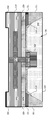
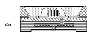
| US11081630B2 (en) | Light emitting device package with a coating layer | |
| US8710513B2 (en) | Light-emitting device package and method of manufacturing the same | |
| KR20120119395A (ko) | 발광소자 패키지 및 그 제조방법 | |
| KR20150092423A (ko) | 발광소자 패키지 | |
| CN108701740A (zh) | 半导体器件和用于制造半导体器件的方法 | |
| CN102144305B (zh) | 光电子部件和制造光电子部件的方法 | |
| TWI506821B (zh) | 發光二極體封裝結構及其製造方法 | |
| JP7193532B2 (ja) | 発光デバイスパッケージ | |
| US20130015488A1 (en) | Light emitting diode package and method for fabricating the same | |
| KR20090104578A (ko) | 발광 다이오드 패키지 | |
| JP2020527864A (ja) | リードフレーム及び絶縁材料を含む発光デバイス | |
| CN104103734A (zh) | 发光二极管封装结构 | |
| KR20090103292A (ko) | Led 패키지 | |
| TW201349600A (zh) | 發光二極體及其封裝方法 | |
| KR101299563B1 (ko) | 반도체 소자 구조물을 제조하는 방법 | |
| KR101863549B1 (ko) | 반도체 발광소자 | |
| TWI404186B (zh) | 半導體組件用之電連接導體、半導體組件以及電連接導體之製造方法 | |
| KR101507132B1 (ko) | 발광 소자 | |
| KR20110131429A (ko) | 발광소자 및 이의 제조방법 | |
| KR101461153B1 (ko) | 반도체 소자 구조물을 제조하는 방법 |
Legal Events
| Date | Code | Title | Description |
|---|---|---|---|
| PA0105 | International application |
Patent event date: 20200518 Patent event code: PA01051R01D Comment text: International Patent Application |
|
| PG1501 | Laying open of application | ||
| AMND | Amendment | ||
| PA0201 | Request for examination |
Patent event code: PA02012R01D Patent event date: 20211001 Comment text: Request for Examination of Application |
|
| E902 | Notification of reason for refusal | ||
| PE0902 | Notice of grounds for rejection |
Comment text: Notification of reason for refusal Patent event date: 20230614 Patent event code: PE09021S01D |
|
| AMND | Amendment | ||
| E601 | Decision to refuse application | ||
| PE0601 | Decision on rejection of patent |
Patent event date: 20231213 Comment text: Decision to Refuse Application Patent event code: PE06012S01D Patent event date: 20230614 Comment text: Notification of reason for refusal Patent event code: PE06011S01I |
|
| X091 | Application refused [patent] | ||
| AMND | Amendment | ||
| PX0901 | Re-examination |
Patent event code: PX09011S01I Patent event date: 20231213 Comment text: Decision to Refuse Application Patent event code: PX09012R01I Patent event date: 20230811 Comment text: Amendment to Specification, etc. Patent event code: PX09012R01I Patent event date: 20211001 Comment text: Amendment to Specification, etc. |
|
| PX0601 | Decision of rejection after re-examination |
Comment text: Decision to Refuse Application Patent event code: PX06014S01D Patent event date: 20240409 Comment text: Amendment to Specification, etc. Patent event code: PX06012R01I Patent event date: 20240314 Comment text: Decision to Refuse Application Patent event code: PX06011S01I Patent event date: 20231213 Comment text: Amendment to Specification, etc. Patent event code: PX06012R01I Patent event date: 20230811 Comment text: Notification of reason for refusal Patent event code: PX06013S01I Patent event date: 20230614 Comment text: Amendment to Specification, etc. Patent event code: PX06012R01I Patent event date: 20211001 |
|
| X601 | Decision of rejection after re-examination |