KR20180098451A - 표시 장치 - Google Patents
표시 장치 Download PDFInfo
- Publication number
- KR20180098451A KR20180098451A KR1020170024982A KR20170024982A KR20180098451A KR 20180098451 A KR20180098451 A KR 20180098451A KR 1020170024982 A KR1020170024982 A KR 1020170024982A KR 20170024982 A KR20170024982 A KR 20170024982A KR 20180098451 A KR20180098451 A KR 20180098451A
- Authority
- KR
- South Korea
- Prior art keywords
- notches
- pad
- region
- wirings
- display device
- Prior art date
- Legal status (The legal status is an assumption and is not a legal conclusion. Google has not performed a legal analysis and makes no representation as to the accuracy of the status listed.)
- Granted
Links
Images


Classifications
-
- H01L27/3276—
-
- H—ELECTRICITY
- H10—SEMICONDUCTOR DEVICES; ELECTRIC SOLID-STATE DEVICES NOT OTHERWISE PROVIDED FOR
- H10K—ORGANIC ELECTRIC SOLID-STATE DEVICES
- H10K59/00—Integrated devices, or assemblies of multiple devices, comprising at least one organic light-emitting element covered by group H10K50/00
- H10K59/10—OLED displays
- H10K59/12—Active-matrix OLED [AMOLED] displays
- H10K59/131—Interconnections, e.g. wiring lines or terminals
-
- H—ELECTRICITY
- H10—SEMICONDUCTOR DEVICES; ELECTRIC SOLID-STATE DEVICES NOT OTHERWISE PROVIDED FOR
- H10K—ORGANIC ELECTRIC SOLID-STATE DEVICES
- H10K59/00—Integrated devices, or assemblies of multiple devices, comprising at least one organic light-emitting element covered by group H10K50/00
-
- G—PHYSICS
- G09—EDUCATION; CRYPTOGRAPHY; DISPLAY; ADVERTISING; SEALS
- G09F—DISPLAYING; ADVERTISING; SIGNS; LABELS OR NAME-PLATES; SEALS
- G09F9/00—Indicating arrangements for variable information in which the information is built-up on a support by selection or combination of individual elements
- G09F9/30—Indicating arrangements for variable information in which the information is built-up on a support by selection or combination of individual elements in which the desired character or characters are formed by combining individual elements
- G09F9/301—Indicating arrangements for variable information in which the information is built-up on a support by selection or combination of individual elements in which the desired character or characters are formed by combining individual elements flexible foldable or roll-able electronic displays, e.g. thin LCD, OLED
-
- G—PHYSICS
- G09—EDUCATION; CRYPTOGRAPHY; DISPLAY; ADVERTISING; SEALS
- G09G—ARRANGEMENTS OR CIRCUITS FOR CONTROL OF INDICATING DEVICES USING STATIC MEANS TO PRESENT VARIABLE INFORMATION
- G09G3/00—Control arrangements or circuits, of interest only in connection with visual indicators other than cathode-ray tubes
- G09G3/20—Control arrangements or circuits, of interest only in connection with visual indicators other than cathode-ray tubes for presentation of an assembly of a number of characters, e.g. a page, by composing the assembly by combination of individual elements arranged in a matrix no fixed position being assigned to or needed to be assigned to the individual characters or partial characters
- G09G3/22—Control arrangements or circuits, of interest only in connection with visual indicators other than cathode-ray tubes for presentation of an assembly of a number of characters, e.g. a page, by composing the assembly by combination of individual elements arranged in a matrix no fixed position being assigned to or needed to be assigned to the individual characters or partial characters using controlled light sources
- G09G3/30—Control arrangements or circuits, of interest only in connection with visual indicators other than cathode-ray tubes for presentation of an assembly of a number of characters, e.g. a page, by composing the assembly by combination of individual elements arranged in a matrix no fixed position being assigned to or needed to be assigned to the individual characters or partial characters using controlled light sources using electroluminescent panels
- G09G3/32—Control arrangements or circuits, of interest only in connection with visual indicators other than cathode-ray tubes for presentation of an assembly of a number of characters, e.g. a page, by composing the assembly by combination of individual elements arranged in a matrix no fixed position being assigned to or needed to be assigned to the individual characters or partial characters using controlled light sources using electroluminescent panels semiconductive, e.g. using light-emitting diodes [LED]
- G09G3/3208—Control arrangements or circuits, of interest only in connection with visual indicators other than cathode-ray tubes for presentation of an assembly of a number of characters, e.g. a page, by composing the assembly by combination of individual elements arranged in a matrix no fixed position being assigned to or needed to be assigned to the individual characters or partial characters using controlled light sources using electroluminescent panels semiconductive, e.g. using light-emitting diodes [LED] organic, e.g. using organic light-emitting diodes [OLED]
- G09G3/3225—Control arrangements or circuits, of interest only in connection with visual indicators other than cathode-ray tubes for presentation of an assembly of a number of characters, e.g. a page, by composing the assembly by combination of individual elements arranged in a matrix no fixed position being assigned to or needed to be assigned to the individual characters or partial characters using controlled light sources using electroluminescent panels semiconductive, e.g. using light-emitting diodes [LED] organic, e.g. using organic light-emitting diodes [OLED] using an active matrix
- G09G3/3233—Control arrangements or circuits, of interest only in connection with visual indicators other than cathode-ray tubes for presentation of an assembly of a number of characters, e.g. a page, by composing the assembly by combination of individual elements arranged in a matrix no fixed position being assigned to or needed to be assigned to the individual characters or partial characters using controlled light sources using electroluminescent panels semiconductive, e.g. using light-emitting diodes [LED] organic, e.g. using organic light-emitting diodes [OLED] using an active matrix with pixel circuitry controlling the current through the light-emitting element
-
- G—PHYSICS
- G09—EDUCATION; CRYPTOGRAPHY; DISPLAY; ADVERTISING; SEALS
- G09G—ARRANGEMENTS OR CIRCUITS FOR CONTROL OF INDICATING DEVICES USING STATIC MEANS TO PRESENT VARIABLE INFORMATION
- G09G3/00—Control arrangements or circuits, of interest only in connection with visual indicators other than cathode-ray tubes
- G09G3/20—Control arrangements or circuits, of interest only in connection with visual indicators other than cathode-ray tubes for presentation of an assembly of a number of characters, e.g. a page, by composing the assembly by combination of individual elements arranged in a matrix no fixed position being assigned to or needed to be assigned to the individual characters or partial characters
- G09G3/22—Control arrangements or circuits, of interest only in connection with visual indicators other than cathode-ray tubes for presentation of an assembly of a number of characters, e.g. a page, by composing the assembly by combination of individual elements arranged in a matrix no fixed position being assigned to or needed to be assigned to the individual characters or partial characters using controlled light sources
- G09G3/30—Control arrangements or circuits, of interest only in connection with visual indicators other than cathode-ray tubes for presentation of an assembly of a number of characters, e.g. a page, by composing the assembly by combination of individual elements arranged in a matrix no fixed position being assigned to or needed to be assigned to the individual characters or partial characters using controlled light sources using electroluminescent panels
- G09G3/32—Control arrangements or circuits, of interest only in connection with visual indicators other than cathode-ray tubes for presentation of an assembly of a number of characters, e.g. a page, by composing the assembly by combination of individual elements arranged in a matrix no fixed position being assigned to or needed to be assigned to the individual characters or partial characters using controlled light sources using electroluminescent panels semiconductive, e.g. using light-emitting diodes [LED]
- G09G3/3208—Control arrangements or circuits, of interest only in connection with visual indicators other than cathode-ray tubes for presentation of an assembly of a number of characters, e.g. a page, by composing the assembly by combination of individual elements arranged in a matrix no fixed position being assigned to or needed to be assigned to the individual characters or partial characters using controlled light sources using electroluminescent panels semiconductive, e.g. using light-emitting diodes [LED] organic, e.g. using organic light-emitting diodes [OLED]
- G09G3/3266—Details of drivers for scan electrodes
-
- G—PHYSICS
- G09—EDUCATION; CRYPTOGRAPHY; DISPLAY; ADVERTISING; SEALS
- G09G—ARRANGEMENTS OR CIRCUITS FOR CONTROL OF INDICATING DEVICES USING STATIC MEANS TO PRESENT VARIABLE INFORMATION
- G09G3/00—Control arrangements or circuits, of interest only in connection with visual indicators other than cathode-ray tubes
- G09G3/20—Control arrangements or circuits, of interest only in connection with visual indicators other than cathode-ray tubes for presentation of an assembly of a number of characters, e.g. a page, by composing the assembly by combination of individual elements arranged in a matrix no fixed position being assigned to or needed to be assigned to the individual characters or partial characters
- G09G3/22—Control arrangements or circuits, of interest only in connection with visual indicators other than cathode-ray tubes for presentation of an assembly of a number of characters, e.g. a page, by composing the assembly by combination of individual elements arranged in a matrix no fixed position being assigned to or needed to be assigned to the individual characters or partial characters using controlled light sources
- G09G3/30—Control arrangements or circuits, of interest only in connection with visual indicators other than cathode-ray tubes for presentation of an assembly of a number of characters, e.g. a page, by composing the assembly by combination of individual elements arranged in a matrix no fixed position being assigned to or needed to be assigned to the individual characters or partial characters using controlled light sources using electroluminescent panels
- G09G3/32—Control arrangements or circuits, of interest only in connection with visual indicators other than cathode-ray tubes for presentation of an assembly of a number of characters, e.g. a page, by composing the assembly by combination of individual elements arranged in a matrix no fixed position being assigned to or needed to be assigned to the individual characters or partial characters using controlled light sources using electroluminescent panels semiconductive, e.g. using light-emitting diodes [LED]
- G09G3/3208—Control arrangements or circuits, of interest only in connection with visual indicators other than cathode-ray tubes for presentation of an assembly of a number of characters, e.g. a page, by composing the assembly by combination of individual elements arranged in a matrix no fixed position being assigned to or needed to be assigned to the individual characters or partial characters using controlled light sources using electroluminescent panels semiconductive, e.g. using light-emitting diodes [LED] organic, e.g. using organic light-emitting diodes [OLED]
- G09G3/3275—Details of drivers for data electrodes
-
- H01L27/3297—
-
- H—ELECTRICITY
- H10—SEMICONDUCTOR DEVICES; ELECTRIC SOLID-STATE DEVICES NOT OTHERWISE PROVIDED FOR
- H10K—ORGANIC ELECTRIC SOLID-STATE DEVICES
- H10K77/00—Constructional details of devices covered by this subclass and not covered by groups H10K10/80, H10K30/80, H10K50/80 or H10K59/80
- H10K77/10—Substrates, e.g. flexible substrates
- H10K77/111—Flexible substrates
-
- H—ELECTRICITY
- H10—SEMICONDUCTOR DEVICES; ELECTRIC SOLID-STATE DEVICES NOT OTHERWISE PROVIDED FOR
- H10W—GENERIC PACKAGES, INTERCONNECTIONS, CONNECTORS OR OTHER CONSTRUCTIONAL DETAILS OF DEVICES COVERED BY CLASS H10
- H10W20/00—Interconnections in chips, wafers or substrates
- H10W20/40—Interconnections external to wafers or substrates, e.g. back-end-of-line [BEOL] metallisations or vias connecting to gate electrodes
- H10W20/41—Interconnections external to wafers or substrates, e.g. back-end-of-line [BEOL] metallisations or vias connecting to gate electrodes characterised by their conductive parts
- H10W20/435—Cross-sectional shapes or dispositions of interconnections
-
- G—PHYSICS
- G09—EDUCATION; CRYPTOGRAPHY; DISPLAY; ADVERTISING; SEALS
- G09G—ARRANGEMENTS OR CIRCUITS FOR CONTROL OF INDICATING DEVICES USING STATIC MEANS TO PRESENT VARIABLE INFORMATION
- G09G2330/00—Aspects of power supply; Aspects of display protection and defect management
- G09G2330/02—Details of power systems and of start or stop of display operation
- G09G2330/028—Generation of voltages supplied to electrode drivers in a matrix display other than LCD
-
- H—ELECTRICITY
- H10—SEMICONDUCTOR DEVICES; ELECTRIC SOLID-STATE DEVICES NOT OTHERWISE PROVIDED FOR
- H10K—ORGANIC ELECTRIC SOLID-STATE DEVICES
- H10K2102/00—Constructional details relating to the organic devices covered by this subclass
- H10K2102/301—Details of OLEDs
- H10K2102/311—Flexible OLED
-
- Y—GENERAL TAGGING OF NEW TECHNOLOGICAL DEVELOPMENTS; GENERAL TAGGING OF CROSS-SECTIONAL TECHNOLOGIES SPANNING OVER SEVERAL SECTIONS OF THE IPC; TECHNICAL SUBJECTS COVERED BY FORMER USPC CROSS-REFERENCE ART COLLECTIONS [XRACs] AND DIGESTS
- Y02—TECHNOLOGIES OR APPLICATIONS FOR MITIGATION OR ADAPTATION AGAINST CLIMATE CHANGE
- Y02E—REDUCTION OF GREENHOUSE GAS [GHG] EMISSIONS, RELATED TO ENERGY GENERATION, TRANSMISSION OR DISTRIBUTION
- Y02E10/00—Energy generation through renewable energy sources
- Y02E10/50—Photovoltaic [PV] energy
- Y02E10/549—Organic PV cells
-
- Y—GENERAL TAGGING OF NEW TECHNOLOGICAL DEVELOPMENTS; GENERAL TAGGING OF CROSS-SECTIONAL TECHNOLOGIES SPANNING OVER SEVERAL SECTIONS OF THE IPC; TECHNICAL SUBJECTS COVERED BY FORMER USPC CROSS-REFERENCE ART COLLECTIONS [XRACs] AND DIGESTS
- Y02—TECHNOLOGIES OR APPLICATIONS FOR MITIGATION OR ADAPTATION AGAINST CLIMATE CHANGE
- Y02P—CLIMATE CHANGE MITIGATION TECHNOLOGIES IN THE PRODUCTION OR PROCESSING OF GOODS
- Y02P70/00—Climate change mitigation technologies in the production process for final industrial or consumer products
- Y02P70/50—Manufacturing or production processes characterised by the final manufactured product
Landscapes
- Engineering & Computer Science (AREA)
- Physics & Mathematics (AREA)
- General Physics & Mathematics (AREA)
- Theoretical Computer Science (AREA)
- Computer Hardware Design (AREA)
- Microelectronics & Electronic Packaging (AREA)
- Devices For Indicating Variable Information By Combining Individual Elements (AREA)
- Electroluminescent Light Sources (AREA)
Abstract
Description
도 2는 도 1의 표시 장치가 전개된 형상의 일 예를 나타내는 단면도이다.
도 3은 도 1의 표시 장치가 벤딩된 형상의 일 예를 나타내는 단면도이다.
도 4는 도 2의 표시 장치의 "C" 영역을 확대 도시한 일 예를 나타내는 단면도이다.
도 5a는 도 2의 표시 장치의 "D" 영역을 확대 도시한 일 예를 나타내는 단면도이다.
도 5b는 도 2의 표시 장치의 "D" 영역을 확대 도시한 다른 예를 나타내는 단면도이다.
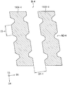
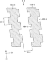
도 6은 도 1의 표시 장치의 "A" 영역을 확대 도시한 일 예를 나타내는 평면도이다.
도 7은 도 6의 벤딩 영역에서 I-I'라인을 따라 절단한 단면도이다.
도 8 내지 도 12는 도 1의 표시 장치의 "A" 영역을 확대 도시한 예들을 나타내는 평면도들이다.
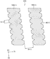
도 13 내지 도 18은 도 1의 표시 장치의 "B" 영역을 확대 도시한 예들을 나타내는 평면도들이다.
도 19 및 도 20은 도 1의 표시 장치의 효과를 설명하기 위한 도면들이다.
NR: 패드 영역 100: 표시 패널
110: 기판 120: 반도체 소자
140: 화소 구조물 170: 박막 봉지 구조물
180: 연결 배선 300: 구동 회로
1000: 표시 장치
Claims (23)
- 표시 영역, 상기 표시 영역으로부터 이격되는 패드 영역, 및 상기 표시 영역과 상기 패드 영역 사이에 위치하는 벤딩 영역을 포함하는 기판;
상기 기판의 상기 표시 영역 상에 배치되는 화소 구조물들;
상기 기판의 상기 패드 영역 상에 배치되는 패드 배선들; 및
상기 패드 배선들과 상기 화소 구조물들을 전기적으로 연결하고, 상기 벤딩 영역 상에서 복수의 노치(notch)들을 각각 포함하는 복수의 연결 배선들을 포함하는 표시 장치. - 제1 항에 있어서, 상기 노치들 중 인접한 두 개의 노치들 사이의 제1 거리는 상기 연결 배선들 중 인접한 두 개의 연결 배선들 사이의 제2 거리보다 작은 것을 특징으로 하는 표시 장치.
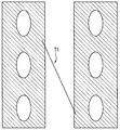
- 제2 항에 있어서, 상기 연결 배선들 각각은 상기 벤딩 영역 상에서 홀(hole)들을 더 포함하는 것을 특징으로 하는 표시 장치.
- 제3 항에 있어서, 상기 홀들 각각의 제1 크기는 상기 제2 거리보다 작은 것을 특징으로 하는 표시 장치.
- 제3 항에 있어서, 상기 연결 배선들은 상기 벤딩 영역 상에서 제1 방향으로 연장되고,
상기 홀들은 상기 제1 방향과 직교하는 제2 방향에서 상기 노치들과 중첩되지 않는 것을 특징으로 하는 표시 장치. - 제1 항에 있어서, 상기 노치들은 상기 연결 배선 각각의 제1 측면에 형성된 제1 노치들 및 상기 제1 측면과 반대되는 제2 측면에 형성된 제2 노치들을 포함하는 것을 특징으로 하는 표시 장치.
- 제6 항에 있어서, 상기 연결 배선들은 상기 벤딩 영역 상에서 제1 방향으로 연장되고,
상기 제1 노치들은 상기 제1 방향과 직교하는 제2 방향에서 상기 제2 노치들과 중첩되지 않는 것을 특징으로 하는 표시 장치. - 제6 항에 있어서, 상기 연결 배선들은 상기 벤딩 영역 상에서 제1 방향으로 연장되고,
상기 제1 노치들은 상기 제1 방향에 대해 상기 제2 노치들에 대칭으로 배치되는 것을 특징으로 하는 표시 장치. - 제1 항에 있어서, 상기 노치들은 삼각형, 사각형, 반원형 중 적어도 하나의 모양을 갖는 것을 특징으로 하는 표시 장치.
- 제1 항에 있어서, 상기 패드 배선들 각각은 제1 측면에 형성된 제3 노치들 및 상기 제1 측면과 반대되는 제2 측면에 형성된 제4 노치들을 포함하는 것을 특징으로 하는 표시 장치.
- 제10 항에 있어서, 상기 패드 배선들은 제3 방향으로 연장되고,
상기 제3 노치들은 상기 제3 방향과 직교하는 제4 방향에서 상기 제4 노치들과 중첩되지 않는 것을 특징으로 하는 표시 장치. - 제10 항에 있어서, 상기 패드 배선들은 제3 방향으로 연장되고,
상기 제3 노치들은 상기 제3 방향에 대해 상기 제4 노치들에 대칭으로 배치되는 것을 특징으로 하는 표시 장치. - 제1 항에 있어서, 상기 연결 배선은,
제1 금속층;
알루미늄(Al)을 포함하고, 상기 제1 금속층 상에 배치되는 제2 금속층; 및
상기 제2 금속층 상에 배치되는 제3 금속층을 포함하는 것을 특징으로 하는 표시 장치. - 제1 항에 있어서, 상기 기판은 상기 벤딩 영역에서 상기 화소 구조물들이 바깥쪽을 향하도록 벤딩되는 것을 특징으로 하는 표시 장치.
- 제1 항에 있어서,
상기 표시 영역 및 상기 패드 영역에 상응하는 상기 표시 패널의 저면 상에 배치되는 하부 보호 필름; 및
상기 기판 및 상기 하부 보호 필름 사이에 배치되는 접착층을 더 포함하는 것을 특징으로 하는 표시 장치. - 제1 항에 있어서, 상기 연결 배선들은 상기 패드 배선들을 통해 데이터 신호, 스캔 신호, 발광 신호, 전원 전압 중 적어도 하나를 수신하는 것을 특징으로 하는 표시 장치.
- 표시 영역, 상기 표시 영역으로부터 이격되는 패드 영역, 및 상기 표시 영역과 상기 패드 영역 사이에 위치하는 벤딩 영역을 포함하는 기판;
상기 기판의 상기 표시 영역 상에 배치되는 화소 구조물들;
상기 화소 구조물들에 구동 신호를 제공하는 구동 회로; 및
상기 구동 회로와 상기 화소 구조물들을 전기적으로 연결하고, 상기 벤딩 영역 상에서 복수의 노치들을 각각 포함하는 복수의 연결 배선들을 포함하는 표시 장치. - 제17 항에 있어서, 상기 노치들 중 인접한 두 개의 노치들 사이의 제1 거리는 상기 연결 배선들 중 인접한 두 개의 연결 배선들 사이의 제2 거리보다 작은 것을 특징으로 하는 표시 장치.
- 제18 항에 있어서, 상기 연결 배선들 각각은 상기 벤딩 영역 상에서 홀들을 더 포함하는 것을 특징으로 하는 표시 장치.
- 제19 항에 있어서, 상기 홀들 각각의 제1 크기는 상기 연결 배선들 중 인접한 두 개의 연결 배선들 사이의 제2 거리보다 작은 것을 특징으로 하는 표시 장치.
- 제17 항에 있어서, 상기 노치들은 상기 연결 배선 각각의 제1 측면에 형성된 제1 노치들 및 상기 제1 측면과 반대되는 제2 측면에 형성된 제2 노치들을 포함하는 것을 특징으로 하는 표시 장치.
- 제17 항에 있어서, 상기 구동 회로는 상기 패드 영역 상에 위치하고,
상기 연결 배선들은 상기 기판의 상기 패드 영역 상에 배치되는 패드 배선들 및 상기 패드 배선들과 연결되는 도전 패턴들을 통해 상기 구동 회로와 연결되는 것을 특징으로 하는 표시 장치. - 제22 항에 있어서, 상기 패드 배선들 각각은 상기 패드 영역 상에서 제1 측면에 형성된 제3 노치들 및 상기 제1 측면과 반대되는 제2 측면에 형성된 제4 노치들을 포함하는 것을 특징으로 하는 표시 장치.
Priority Applications (7)
| Application Number | Priority Date | Filing Date | Title |
|---|---|---|---|
| KR1020170024982A KR102783141B1 (ko) | 2017-02-24 | 2017-02-24 | 표시 장치 |
| US15/661,122 US10269890B2 (en) | 2017-02-24 | 2017-07-27 | Display device having notched connection wiring |
| EP20160773.6A EP3686934B1 (en) | 2017-02-24 | 2017-10-24 | Display device having notched connection wiring |
| EP17198097.2A EP3367440B1 (en) | 2017-02-24 | 2017-10-24 | Display device having notched connection wiring |
| CN201711054499.4A CN108511483B (zh) | 2017-02-24 | 2017-11-01 | 具有带凹口的连接布线的显示装置 |
| US16/358,322 US10748980B2 (en) | 2017-02-24 | 2019-03-19 | Display device having notched connection wiring |
| US16/928,807 US11342405B2 (en) | 2017-02-24 | 2020-07-14 | Display device having notched connection wiring |
Applications Claiming Priority (1)
| Application Number | Priority Date | Filing Date | Title |
|---|---|---|---|
| KR1020170024982A KR102783141B1 (ko) | 2017-02-24 | 2017-02-24 | 표시 장치 |
Publications (2)
| Publication Number | Publication Date |
|---|---|
| KR20180098451A true KR20180098451A (ko) | 2018-09-04 |
| KR102783141B1 KR102783141B1 (ko) | 2025-03-20 |
Family
ID=60186053
Family Applications (1)
| Application Number | Title | Priority Date | Filing Date |
|---|---|---|---|
| KR1020170024982A Active KR102783141B1 (ko) | 2017-02-24 | 2017-02-24 | 표시 장치 |
Country Status (4)
| Country | Link |
|---|---|
| US (3) | US10269890B2 (ko) |
| EP (2) | EP3686934B1 (ko) |
| KR (1) | KR102783141B1 (ko) |
| CN (1) | CN108511483B (ko) |
Families Citing this family (19)
| Publication number | Priority date | Publication date | Assignee | Title |
|---|---|---|---|---|
| KR102783141B1 (ko) | 2017-02-24 | 2025-03-20 | 삼성디스플레이 주식회사 | 표시 장치 |
| JP2018205337A (ja) * | 2017-05-30 | 2018-12-27 | 株式会社ジャパンディスプレイ | 表示装置 |
| KR102337750B1 (ko) * | 2017-11-06 | 2021-12-10 | 삼성디스플레이 주식회사 | 표시 장치 및 이의 제조 방법 |
| CN108565268B (zh) * | 2018-04-02 | 2021-02-12 | 昆山国显光电有限公司 | 阵列基板及显示屏 |
| CN109494314B (zh) * | 2018-10-16 | 2020-12-08 | 武汉华星光电半导体显示技术有限公司 | 一种柔性oled显示面板及其制备方法 |
| CN109585700B (zh) * | 2018-12-14 | 2020-06-19 | 京东方科技集团股份有限公司 | 一种显示基板及其制作方法、显示装置 |
| CN109599403B (zh) * | 2018-12-19 | 2021-02-26 | 武汉华星光电半导体显示技术有限公司 | 金属走线 |
| CN109638060B (zh) * | 2018-12-21 | 2020-10-27 | 武汉华星光电半导体显示技术有限公司 | 阵列基板及柔性显示面板 |
| CN109655957B (zh) * | 2019-01-08 | 2021-06-22 | 昆山工研院新型平板显示技术中心有限公司 | 偏光片及其制作方法、显示面板和显示设备 |
| KR102688018B1 (ko) * | 2019-05-13 | 2024-07-25 | 삼성디스플레이 주식회사 | 입력 감지 유닛, 그것을 포함하는 표시 장치 및 그것의 제조 방법 |
| CN110335544B (zh) * | 2019-06-18 | 2020-12-25 | 武汉华星光电半导体显示技术有限公司 | Oled显示面板及显示装置 |
| KR102752716B1 (ko) * | 2019-10-28 | 2025-01-08 | 엘지디스플레이 주식회사 | 플렉서블 표시 장치 |
| CN110767731B (zh) * | 2019-10-31 | 2022-05-20 | 京东方科技集团股份有限公司 | 显示面板及显示装置 |
| CN111009565B (zh) * | 2019-12-11 | 2022-06-17 | 昆山国显光电有限公司 | 显示基板、显示基板的制作方法及显示面板 |
| KR102923874B1 (ko) | 2020-02-11 | 2026-02-09 | 삼성디스플레이 주식회사 | 표시 장치 |
| EP4165448B1 (en) * | 2020-06-11 | 2025-09-03 | Signify Holding B.V. | Lens plate |
| CN111580313B (zh) * | 2020-06-16 | 2022-09-02 | 京东方科技集团股份有限公司 | 阵列基板、显示模组、电子设备和阵列基板的制造方法 |
| WO2023162094A1 (ja) * | 2022-02-24 | 2023-08-31 | シャープディスプレイテクノロジー株式会社 | 表示装置 |
| CN114628062B (zh) * | 2022-03-28 | 2023-06-02 | Tcl华星光电技术有限公司 | 一种导电薄膜及显示面板 |
Citations (1)
| Publication number | Priority date | Publication date | Assignee | Title |
|---|---|---|---|---|
| US20160035812A1 (en) * | 2014-07-31 | 2016-02-04 | Lg Display Co., Ltd. | Flexible display device with wire having reinforced portion and manufacturing method for the same |
Family Cites Families (16)
| Publication number | Priority date | Publication date | Assignee | Title |
|---|---|---|---|---|
| JPH06216475A (ja) * | 1993-01-21 | 1994-08-05 | Matsushita Electric Ind Co Ltd | フレキシブル基板 |
| EP1388171A1 (en) * | 2001-05-03 | 2004-02-11 | Koninklijke Philips Electronics N.V. | Electroluminescent device |
| WO2010086033A1 (en) * | 2009-01-30 | 2010-08-05 | Interuniversitair Microelektronica Centrum Vzw | Stretchable electronic device |
| WO2011148664A1 (ja) | 2010-05-24 | 2011-12-01 | シャープ株式会社 | アクティブマトリクス基板及び液晶表示装置 |
| TWI419094B (zh) * | 2010-09-10 | 2013-12-11 | Au Optronics Corp | 可撓性顯示面板 |
| KR101931338B1 (ko) | 2011-10-19 | 2018-12-21 | 엘지디스플레이 주식회사 | 연성회로기판과 이를 이용한 표시장치 |
| US9203050B2 (en) | 2013-05-21 | 2015-12-01 | Samsung Display Co., Ltd. | Organic light emitting diode display and method of manufacturing the same |
| US9788789B2 (en) * | 2013-08-30 | 2017-10-17 | Thalmic Labs Inc. | Systems, articles, and methods for stretchable printed circuit boards |
| KR102085961B1 (ko) | 2013-12-24 | 2020-03-06 | 엘지디스플레이 주식회사 | 플렉서블 유기 발광 표시 장치 및 플렉서블 유기 발광 표시 장치 제조 방법 |
| JP6285275B2 (ja) | 2014-04-30 | 2018-02-28 | 株式会社Screenホールディングス | 基板処理装置および基板処理方法 |
| US20160003581A1 (en) * | 2014-07-03 | 2016-01-07 | David Warren | Plate carrier and a protective vest |
| US9349758B2 (en) | 2014-09-30 | 2016-05-24 | Lg Display Co., Ltd. | Flexible display device with divided power lines and manufacturing method for the same |
| US20160105950A1 (en) * | 2014-10-10 | 2016-04-14 | Apple Inc. | Electronic Device Having Structured Flexible Substrates With Bends |
| KR20160125593A (ko) | 2015-04-21 | 2016-11-01 | 삼성디스플레이 주식회사 | 플렉서블 표시장치 |
| KR102583831B1 (ko) * | 2016-11-25 | 2023-09-27 | 엘지디스플레이 주식회사 | 플렉서블 전계발광 표시장치 |
| KR102783141B1 (ko) | 2017-02-24 | 2025-03-20 | 삼성디스플레이 주식회사 | 표시 장치 |
-
2017
- 2017-02-24 KR KR1020170024982A patent/KR102783141B1/ko active Active
- 2017-07-27 US US15/661,122 patent/US10269890B2/en active Active
- 2017-10-24 EP EP20160773.6A patent/EP3686934B1/en active Active
- 2017-10-24 EP EP17198097.2A patent/EP3367440B1/en active Active
- 2017-11-01 CN CN201711054499.4A patent/CN108511483B/zh active Active
-
2019
- 2019-03-19 US US16/358,322 patent/US10748980B2/en active Active
-
2020
- 2020-07-14 US US16/928,807 patent/US11342405B2/en active Active
Patent Citations (1)
| Publication number | Priority date | Publication date | Assignee | Title |
|---|---|---|---|---|
| US20160035812A1 (en) * | 2014-07-31 | 2016-02-04 | Lg Display Co., Ltd. | Flexible display device with wire having reinforced portion and manufacturing method for the same |
Also Published As
| Publication number | Publication date |
|---|---|
| US11342405B2 (en) | 2022-05-24 |
| KR102783141B1 (ko) | 2025-03-20 |
| EP3367440A1 (en) | 2018-08-29 |
| EP3686934B1 (en) | 2025-06-04 |
| US10269890B2 (en) | 2019-04-23 |
| US10748980B2 (en) | 2020-08-18 |
| EP3686934A1 (en) | 2020-07-29 |
| US20180247992A1 (en) | 2018-08-30 |
| EP3367440B1 (en) | 2020-04-22 |
| US20190214453A1 (en) | 2019-07-11 |
| US20200343333A1 (en) | 2020-10-29 |
| CN108511483A (zh) | 2018-09-07 |
| CN108511483B (zh) | 2023-09-19 |
Similar Documents
| Publication | Publication Date | Title |
|---|---|---|
| KR102783141B1 (ko) | 표시 장치 | |
| CN111129270B (zh) | 微型led显示装置 | |
| CN112951867B (zh) | 显示装置 | |
| CN108962947B (zh) | 一种柔性显示面板和显示装置 | |
| US9978823B2 (en) | Organic light emitting display device and method for manufacturing the same | |
| KR102903911B1 (ko) | 표시 장치 및 이의 제조 방법 | |
| CN108153442A (zh) | 触控显示设备 | |
| JP2019046175A (ja) | 表示装置 | |
| CN104347673A (zh) | 有机发光显示装置及其制造方法 | |
| KR20170012664A (ko) | 박막 트랜지스터 어레이 기판 및 이를 포함하는 유기발광 표시장치 | |
| CN103633112A (zh) | 有机发光二极管显示设备 | |
| CN114503274A (zh) | 显示基板及显示装置 | |
| CN113517262A (zh) | 显示面板及其制作方法、显示装置 | |
| CN114664911A (zh) | 显示基板及显示装置 | |
| JP2015015114A (ja) | 有機エレクトロルミネッセンス表示装置 | |
| CN120548068A (zh) | 显示面板、显示装置及设备 | |
| CN114356154B (zh) | 一种触控基板及显示装置 | |
| KR102466918B1 (ko) | 칩 온 필름 패키지 및 칩 온 필름 패키지를 포함하는 표시 장치 | |
| KR20230102354A (ko) | 표시 장치 | |
| CN116471879A (zh) | 显示装置和制造该显示装置的方法 | |
| CN115458534A (zh) | 显示模组、显示装置 | |
| KR20180079481A (ko) | 유기 발광 표시 장치 | |
| KR20220130286A (ko) | 표시 장치 및 이의 제조 방법 | |
| US20230145007A1 (en) | Display device | |
| US12426412B2 (en) | Display device |
Legal Events
| Date | Code | Title | Description |
|---|---|---|---|
| PA0109 | Patent application |
St.27 status event code: A-0-1-A10-A12-nap-PA0109 |
|
| PG1501 | Laying open of application |
St.27 status event code: A-1-1-Q10-Q12-nap-PG1501 |
|
| R18-X000 | Changes to party contact information recorded |
St.27 status event code: A-3-3-R10-R18-oth-X000 |
|
| P22-X000 | Classification modified |
St.27 status event code: A-2-2-P10-P22-nap-X000 |
|
| P22-X000 | Classification modified |
St.27 status event code: A-2-2-P10-P22-nap-X000 |
|
| A201 | Request for examination | ||
| PA0201 | Request for examination |
St.27 status event code: A-1-2-D10-D11-exm-PA0201 |
|
| P22-X000 | Classification modified |
St.27 status event code: A-2-2-P10-P22-nap-X000 |
|
| P22-X000 | Classification modified |
St.27 status event code: A-2-2-P10-P22-nap-X000 |
|
| E902 | Notification of reason for refusal | ||
| PE0902 | Notice of grounds for rejection |
St.27 status event code: A-1-2-D10-D21-exm-PE0902 |
|
| E13-X000 | Pre-grant limitation requested |
St.27 status event code: A-2-3-E10-E13-lim-X000 |
|
| P11-X000 | Amendment of application requested |
St.27 status event code: A-2-2-P10-P11-nap-X000 |
|
| P13-X000 | Application amended |
St.27 status event code: A-2-2-P10-P13-nap-X000 |
|
| P22-X000 | Classification modified |
St.27 status event code: A-2-2-P10-P22-nap-X000 |
|
| E701 | Decision to grant or registration of patent right | ||
| PE0701 | Decision of registration |
St.27 status event code: A-1-2-D10-D22-exm-PE0701 |
|
| PR0701 | Registration of establishment |
St.27 status event code: A-2-4-F10-F11-exm-PR0701 |
|
| PR1002 | Payment of registration fee |
St.27 status event code: A-2-2-U10-U11-oth-PR1002 |
|
| PG1601 | Publication of registration |
St.27 status event code: A-4-4-Q10-Q13-nap-PG1601 |