KR20180098451A - Display device - Google Patents
Display device Download PDFInfo
- Publication number
- KR20180098451A KR20180098451A KR1020170024982A KR20170024982A KR20180098451A KR 20180098451 A KR20180098451 A KR 20180098451A KR 1020170024982 A KR1020170024982 A KR 1020170024982A KR 20170024982 A KR20170024982 A KR 20170024982A KR 20180098451 A KR20180098451 A KR 20180098451A
- Authority
- KR
- South Korea
- Prior art keywords
- notches
- pad
- region
- wirings
- display device
- Prior art date
- Legal status (The legal status is an assumption and is not a legal conclusion. Google has not performed a legal analysis and makes no representation as to the accuracy of the status listed.)
- Granted
Links
Images


Classifications
-
- H01L27/3276—
-
- H—ELECTRICITY
- H10—SEMICONDUCTOR DEVICES; ELECTRIC SOLID-STATE DEVICES NOT OTHERWISE PROVIDED FOR
- H10K—ORGANIC ELECTRIC SOLID-STATE DEVICES
- H10K59/00—Integrated devices, or assemblies of multiple devices, comprising at least one organic light-emitting element covered by group H10K50/00
- H10K59/10—OLED displays
- H10K59/12—Active-matrix OLED [AMOLED] displays
- H10K59/131—Interconnections, e.g. wiring lines or terminals
-
- H—ELECTRICITY
- H10—SEMICONDUCTOR DEVICES; ELECTRIC SOLID-STATE DEVICES NOT OTHERWISE PROVIDED FOR
- H10K—ORGANIC ELECTRIC SOLID-STATE DEVICES
- H10K59/00—Integrated devices, or assemblies of multiple devices, comprising at least one organic light-emitting element covered by group H10K50/00
-
- G—PHYSICS
- G09—EDUCATION; CRYPTOGRAPHY; DISPLAY; ADVERTISING; SEALS
- G09F—DISPLAYING; ADVERTISING; SIGNS; LABELS OR NAME-PLATES; SEALS
- G09F9/00—Indicating arrangements for variable information in which the information is built-up on a support by selection or combination of individual elements
- G09F9/30—Indicating arrangements for variable information in which the information is built-up on a support by selection or combination of individual elements in which the desired character or characters are formed by combining individual elements
- G09F9/301—Indicating arrangements for variable information in which the information is built-up on a support by selection or combination of individual elements in which the desired character or characters are formed by combining individual elements flexible foldable or roll-able electronic displays, e.g. thin LCD, OLED
-
- G—PHYSICS
- G09—EDUCATION; CRYPTOGRAPHY; DISPLAY; ADVERTISING; SEALS
- G09G—ARRANGEMENTS OR CIRCUITS FOR CONTROL OF INDICATING DEVICES USING STATIC MEANS TO PRESENT VARIABLE INFORMATION
- G09G3/00—Control arrangements or circuits, of interest only in connection with visual indicators other than cathode-ray tubes
- G09G3/20—Control arrangements or circuits, of interest only in connection with visual indicators other than cathode-ray tubes for presentation of an assembly of a number of characters, e.g. a page, by composing the assembly by combination of individual elements arranged in a matrix no fixed position being assigned to or needed to be assigned to the individual characters or partial characters
- G09G3/22—Control arrangements or circuits, of interest only in connection with visual indicators other than cathode-ray tubes for presentation of an assembly of a number of characters, e.g. a page, by composing the assembly by combination of individual elements arranged in a matrix no fixed position being assigned to or needed to be assigned to the individual characters or partial characters using controlled light sources
- G09G3/30—Control arrangements or circuits, of interest only in connection with visual indicators other than cathode-ray tubes for presentation of an assembly of a number of characters, e.g. a page, by composing the assembly by combination of individual elements arranged in a matrix no fixed position being assigned to or needed to be assigned to the individual characters or partial characters using controlled light sources using electroluminescent panels
- G09G3/32—Control arrangements or circuits, of interest only in connection with visual indicators other than cathode-ray tubes for presentation of an assembly of a number of characters, e.g. a page, by composing the assembly by combination of individual elements arranged in a matrix no fixed position being assigned to or needed to be assigned to the individual characters or partial characters using controlled light sources using electroluminescent panels semiconductive, e.g. using light-emitting diodes [LED]
- G09G3/3208—Control arrangements or circuits, of interest only in connection with visual indicators other than cathode-ray tubes for presentation of an assembly of a number of characters, e.g. a page, by composing the assembly by combination of individual elements arranged in a matrix no fixed position being assigned to or needed to be assigned to the individual characters or partial characters using controlled light sources using electroluminescent panels semiconductive, e.g. using light-emitting diodes [LED] organic, e.g. using organic light-emitting diodes [OLED]
- G09G3/3225—Control arrangements or circuits, of interest only in connection with visual indicators other than cathode-ray tubes for presentation of an assembly of a number of characters, e.g. a page, by composing the assembly by combination of individual elements arranged in a matrix no fixed position being assigned to or needed to be assigned to the individual characters or partial characters using controlled light sources using electroluminescent panels semiconductive, e.g. using light-emitting diodes [LED] organic, e.g. using organic light-emitting diodes [OLED] using an active matrix
- G09G3/3233—Control arrangements or circuits, of interest only in connection with visual indicators other than cathode-ray tubes for presentation of an assembly of a number of characters, e.g. a page, by composing the assembly by combination of individual elements arranged in a matrix no fixed position being assigned to or needed to be assigned to the individual characters or partial characters using controlled light sources using electroluminescent panels semiconductive, e.g. using light-emitting diodes [LED] organic, e.g. using organic light-emitting diodes [OLED] using an active matrix with pixel circuitry controlling the current through the light-emitting element
-
- G—PHYSICS
- G09—EDUCATION; CRYPTOGRAPHY; DISPLAY; ADVERTISING; SEALS
- G09G—ARRANGEMENTS OR CIRCUITS FOR CONTROL OF INDICATING DEVICES USING STATIC MEANS TO PRESENT VARIABLE INFORMATION
- G09G3/00—Control arrangements or circuits, of interest only in connection with visual indicators other than cathode-ray tubes
- G09G3/20—Control arrangements or circuits, of interest only in connection with visual indicators other than cathode-ray tubes for presentation of an assembly of a number of characters, e.g. a page, by composing the assembly by combination of individual elements arranged in a matrix no fixed position being assigned to or needed to be assigned to the individual characters or partial characters
- G09G3/22—Control arrangements or circuits, of interest only in connection with visual indicators other than cathode-ray tubes for presentation of an assembly of a number of characters, e.g. a page, by composing the assembly by combination of individual elements arranged in a matrix no fixed position being assigned to or needed to be assigned to the individual characters or partial characters using controlled light sources
- G09G3/30—Control arrangements or circuits, of interest only in connection with visual indicators other than cathode-ray tubes for presentation of an assembly of a number of characters, e.g. a page, by composing the assembly by combination of individual elements arranged in a matrix no fixed position being assigned to or needed to be assigned to the individual characters or partial characters using controlled light sources using electroluminescent panels
- G09G3/32—Control arrangements or circuits, of interest only in connection with visual indicators other than cathode-ray tubes for presentation of an assembly of a number of characters, e.g. a page, by composing the assembly by combination of individual elements arranged in a matrix no fixed position being assigned to or needed to be assigned to the individual characters or partial characters using controlled light sources using electroluminescent panels semiconductive, e.g. using light-emitting diodes [LED]
- G09G3/3208—Control arrangements or circuits, of interest only in connection with visual indicators other than cathode-ray tubes for presentation of an assembly of a number of characters, e.g. a page, by composing the assembly by combination of individual elements arranged in a matrix no fixed position being assigned to or needed to be assigned to the individual characters or partial characters using controlled light sources using electroluminescent panels semiconductive, e.g. using light-emitting diodes [LED] organic, e.g. using organic light-emitting diodes [OLED]
- G09G3/3266—Details of drivers for scan electrodes
-
- G—PHYSICS
- G09—EDUCATION; CRYPTOGRAPHY; DISPLAY; ADVERTISING; SEALS
- G09G—ARRANGEMENTS OR CIRCUITS FOR CONTROL OF INDICATING DEVICES USING STATIC MEANS TO PRESENT VARIABLE INFORMATION
- G09G3/00—Control arrangements or circuits, of interest only in connection with visual indicators other than cathode-ray tubes
- G09G3/20—Control arrangements or circuits, of interest only in connection with visual indicators other than cathode-ray tubes for presentation of an assembly of a number of characters, e.g. a page, by composing the assembly by combination of individual elements arranged in a matrix no fixed position being assigned to or needed to be assigned to the individual characters or partial characters
- G09G3/22—Control arrangements or circuits, of interest only in connection with visual indicators other than cathode-ray tubes for presentation of an assembly of a number of characters, e.g. a page, by composing the assembly by combination of individual elements arranged in a matrix no fixed position being assigned to or needed to be assigned to the individual characters or partial characters using controlled light sources
- G09G3/30—Control arrangements or circuits, of interest only in connection with visual indicators other than cathode-ray tubes for presentation of an assembly of a number of characters, e.g. a page, by composing the assembly by combination of individual elements arranged in a matrix no fixed position being assigned to or needed to be assigned to the individual characters or partial characters using controlled light sources using electroluminescent panels
- G09G3/32—Control arrangements or circuits, of interest only in connection with visual indicators other than cathode-ray tubes for presentation of an assembly of a number of characters, e.g. a page, by composing the assembly by combination of individual elements arranged in a matrix no fixed position being assigned to or needed to be assigned to the individual characters or partial characters using controlled light sources using electroluminescent panels semiconductive, e.g. using light-emitting diodes [LED]
- G09G3/3208—Control arrangements or circuits, of interest only in connection with visual indicators other than cathode-ray tubes for presentation of an assembly of a number of characters, e.g. a page, by composing the assembly by combination of individual elements arranged in a matrix no fixed position being assigned to or needed to be assigned to the individual characters or partial characters using controlled light sources using electroluminescent panels semiconductive, e.g. using light-emitting diodes [LED] organic, e.g. using organic light-emitting diodes [OLED]
- G09G3/3275—Details of drivers for data electrodes
-
- H01L27/3297—
-
- H—ELECTRICITY
- H10—SEMICONDUCTOR DEVICES; ELECTRIC SOLID-STATE DEVICES NOT OTHERWISE PROVIDED FOR
- H10K—ORGANIC ELECTRIC SOLID-STATE DEVICES
- H10K77/00—Constructional details of devices covered by this subclass and not covered by groups H10K10/80, H10K30/80, H10K50/80 or H10K59/80
- H10K77/10—Substrates, e.g. flexible substrates
- H10K77/111—Flexible substrates
-
- H—ELECTRICITY
- H10—SEMICONDUCTOR DEVICES; ELECTRIC SOLID-STATE DEVICES NOT OTHERWISE PROVIDED FOR
- H10W—GENERIC PACKAGES, INTERCONNECTIONS, CONNECTORS OR OTHER CONSTRUCTIONAL DETAILS OF DEVICES COVERED BY CLASS H10
- H10W20/00—Interconnections in chips, wafers or substrates
- H10W20/40—Interconnections external to wafers or substrates, e.g. back-end-of-line [BEOL] metallisations or vias connecting to gate electrodes
- H10W20/41—Interconnections external to wafers or substrates, e.g. back-end-of-line [BEOL] metallisations or vias connecting to gate electrodes characterised by their conductive parts
- H10W20/435—Cross-sectional shapes or dispositions of interconnections
-
- G—PHYSICS
- G09—EDUCATION; CRYPTOGRAPHY; DISPLAY; ADVERTISING; SEALS
- G09G—ARRANGEMENTS OR CIRCUITS FOR CONTROL OF INDICATING DEVICES USING STATIC MEANS TO PRESENT VARIABLE INFORMATION
- G09G2330/00—Aspects of power supply; Aspects of display protection and defect management
- G09G2330/02—Details of power systems and of start or stop of display operation
- G09G2330/028—Generation of voltages supplied to electrode drivers in a matrix display other than LCD
-
- H—ELECTRICITY
- H10—SEMICONDUCTOR DEVICES; ELECTRIC SOLID-STATE DEVICES NOT OTHERWISE PROVIDED FOR
- H10K—ORGANIC ELECTRIC SOLID-STATE DEVICES
- H10K2102/00—Constructional details relating to the organic devices covered by this subclass
- H10K2102/301—Details of OLEDs
- H10K2102/311—Flexible OLED
-
- Y—GENERAL TAGGING OF NEW TECHNOLOGICAL DEVELOPMENTS; GENERAL TAGGING OF CROSS-SECTIONAL TECHNOLOGIES SPANNING OVER SEVERAL SECTIONS OF THE IPC; TECHNICAL SUBJECTS COVERED BY FORMER USPC CROSS-REFERENCE ART COLLECTIONS [XRACs] AND DIGESTS
- Y02—TECHNOLOGIES OR APPLICATIONS FOR MITIGATION OR ADAPTATION AGAINST CLIMATE CHANGE
- Y02E—REDUCTION OF GREENHOUSE GAS [GHG] EMISSIONS, RELATED TO ENERGY GENERATION, TRANSMISSION OR DISTRIBUTION
- Y02E10/00—Energy generation through renewable energy sources
- Y02E10/50—Photovoltaic [PV] energy
- Y02E10/549—Organic PV cells
-
- Y—GENERAL TAGGING OF NEW TECHNOLOGICAL DEVELOPMENTS; GENERAL TAGGING OF CROSS-SECTIONAL TECHNOLOGIES SPANNING OVER SEVERAL SECTIONS OF THE IPC; TECHNICAL SUBJECTS COVERED BY FORMER USPC CROSS-REFERENCE ART COLLECTIONS [XRACs] AND DIGESTS
- Y02—TECHNOLOGIES OR APPLICATIONS FOR MITIGATION OR ADAPTATION AGAINST CLIMATE CHANGE
- Y02P—CLIMATE CHANGE MITIGATION TECHNOLOGIES IN THE PRODUCTION OR PROCESSING OF GOODS
- Y02P70/00—Climate change mitigation technologies in the production process for final industrial or consumer products
- Y02P70/50—Manufacturing or production processes characterised by the final manufactured product
Landscapes
- Engineering & Computer Science (AREA)
- Physics & Mathematics (AREA)
- General Physics & Mathematics (AREA)
- Theoretical Computer Science (AREA)
- Computer Hardware Design (AREA)
- Microelectronics & Electronic Packaging (AREA)
- Devices For Indicating Variable Information By Combining Individual Elements (AREA)
- Electroluminescent Light Sources (AREA)
Abstract
Description
본 발명은 표시 장치에 관한 것으로, 보다 상세하게는 제조 과정에서의 단락 등의 불량 발생을 최소화할 수 있는 표시 장치에 관한 것이다.BACKGROUND OF THE
평판 표시 장치는 경량 및 박형 등의 특성으로 인하여, 음극선관 표시 장치를 대체하는 표시 장치로써 사용되고 있다. 이러한 평판 표시 장치의 대표적인 예로서 액정 표시 장치와 유기 발광 표시 장치가 있다.The flat panel display device is used as a display device for replacing the cathode ray tube display device because of its light weight and thin characteristics. As typical examples of such flat panel display devices, there are a liquid crystal display device and an organic light emitting display device.
최근, 유기 발광 표시 장치에 포함된 표시 패널의 하부 기판과 상부 기판을 플렉서블(flexible)한 재료로 구성함으로써 표시 패널의 일부가 벤딩(bending) 또는 폴딩(folding)될 수 있는 표시 장치가 개발되고 있다. 예를 들어, 표시 패널에 포함된 하부 기판은 플렉서블한 기판으로 구성될 수 있고, 표시 패널에 포함된 상부 기판은 박막 봉지 구조물을 가질 수 있다. In recent years, a display device has been developed in which a part of a display panel can be bended or folded by constituting a lower substrate and an upper substrate of a display panel included in an organic light emitting display device from a flexible material . For example, the lower substrate included in the display panel may be composed of a flexible substrate, and the upper substrate included in the display panel may have a thin film encapsulation structure.
표시 장치는 기판의 적어도 일부를 벤딩시킴으로써, 다양한 각도에서의 시인성을 향상시키거나 비표시 영역의 면적을 줄일 수 있다. 하지만, 벤딩된 표시 장치를 제조하는 과정에서 단락 등의 불량이 발생할 수 있다.By bending at least a part of the substrate, the display device can improve the visibility at various angles or reduce the area of the non-display area. However, defects such as a short circuit may occur in the process of manufacturing a bent display device.
본 발명의 일 목적은 벤딩 영역에서 인접한 배선들 사이의 단락을 방지할 수 있는 표시 장치를 제공하는 것이다.It is an object of the present invention to provide a display device capable of preventing a short circuit between adjacent wirings in a bending region.
다만, 본 발명의 목적은 상기 목적들로 한정되는 것이 아니며, 본 발명의 사상 및 영역으로부터 벗어나지 않는 범위에서 다양하게 확장될 수 있을 것이다.It should be understood, however, that the present invention is not limited to the above-described embodiments, and may be variously modified without departing from the spirit and scope of the present invention.
본 발명의 일 목적을 달성하기 위하여, 본 발명의 실시예들에 따른 표시 장치는 표시 영역, 상기 표시 영역으로부터 이격되는 패드 영역, 및 상기 표시 영역과 상기 패드 영역 사이에 위치하는 벤딩 영역을 포함하는 기판, 상기 기판의 상기 표시 영역 상에 배치되는 화소 구조물들, 상기 기판의 상기 패드 영역 상에 배치되는 패드 배선들, 및 상기 패드 배선들과 상기 화소 구조물들을 전기적으로 연결하고, 상기 벤딩 영역 상에서 복수의 노치(notch)들을 각각 포함하는 복수의 연결 배선들을 포함할 수 있다.In order to accomplish one object of the present invention, a display device according to embodiments of the present invention includes a display area, a pad area spaced from the display area, and a bending area located between the display area and the pad area A display device, comprising: a substrate; pixel structures disposed on the display region of the substrate; pad wirings disposed on the pad region of the substrate; and electrically connecting the pad wirings to the pixel structures, And may include a plurality of connection wires each including notches of a plurality of connection wires.
일 실시예에 의하면, 상기 노치들 중 인접한 두 개의 노치들 사이의 제1 거리는 상기 연결 배선들 중 인접한 두 개의 연결 배선들 사이의 제2 거리보다 작을 수 있다.According to one embodiment, a first distance between two adjacent notches of the notches may be less than a second distance between two adjacent connection wirings of the connection wirings.
일 실시예에 의하면, 상기 연결 배선들 각각은 상기 벤딩 영역 상에서 홀(hole)들을 더 포함할 수 있다.According to one embodiment, each of the connection wirings may further include holes on the bending region.
일 실시예에 의하면, 상기 홀들 각각의 제1 크기는 상기 제2 거리보다 작을 수 있다.According to one embodiment, the first dimension of each of the holes may be smaller than the second distance.
일 실시예에 의하면, 상기 연결 배선들은 상기 벤딩 영역 상에서 제1 방향으로 연장될 수 있다. 상기 홀들은 상기 제1 방향과 직교하는 제2 방향에서 상기 노치들과 중첩되지 않을 수 있다.According to one embodiment, the interconnecting lines may extend in the first direction on the bending region. The holes may not overlap with the notches in a second direction orthogonal to the first direction.
일 실시예에 의하면, 상기 노치들은 상기 연결 배선 각각의 제1 측면에 형성된 제1 노치들 및 상기 제1 측면과 반대되는 제2 측면에 형성된 제2 노치들을 포함할 수 있다.According to one embodiment, the notches may include first notches formed on a first side of each of the interconnecting interconnects, and second notches formed on a second side opposite the first side.
일 실시예에 의하면, 상기 연결 배선들은 상기 벤딩 영역 상에서 제1 방향으로 연장될 수 있다. 상기 제1 노치들은 상기 제1 방향과 직교하는 제2 방향에서 상기 제2 노치들과 중첩되지 않을 수 있다.According to one embodiment, the interconnecting lines may extend in the first direction on the bending region. The first notches may not overlap the second notches in a second direction perpendicular to the first direction.
일 실시예에 의하면, 상기 연결 배선들은 상기 벤딩 영역 상에서 제1 방향으로 연장될 수 있다. 상기 제1 노치들은 상기 제1 방향에 대해 상기 제2 노치들에 대칭으로 배치될 수 있다.According to one embodiment, the interconnecting lines may extend in the first direction on the bending region. The first notches may be disposed symmetrically to the second notches with respect to the first direction.
일 실시예에 의하면, 상기 노치들은 삼각형, 사각형, 반원형 중 적어도 하나의 모양을 가질 수 있다.According to one embodiment, the notches may have a shape of at least one of triangular, rectangular, and semicircular.
일 실시예에 의하면, 상기 패드 배선들 각각은 제1 측면에 형성된 제3 노치들 및 상기 제1 측면과 반대되는 제2 측면에 형성된 제4 노치들을 포함할 수 있다.According to an embodiment, each of the pad wirings may include third notches formed on the first side and fourth notches formed on the second side opposite to the first side.
일 실시예에 의하면, 상기 패드 배선들은 제3 방향으로 연장될 수 있다. 상기 제3 노치들은 상기 제3 방향과 직교하는 제4 방향에서 상기 제4 노치들과 중첩되지 않을 수 있다.According to an embodiment, the pad wirings may extend in a third direction. The third notches may not overlap with the fourth notches in a fourth direction orthogonal to the third direction.
일 실시예에 의하면, 상기 패드 배선들은 제3 방향으로 연장될 수 있다. 상기 제3 노치들은 상기 제3 방향에 대해 상기 제4 노치들에 대칭으로 배치될 수 있다.According to an embodiment, the pad wirings may extend in a third direction. The third notches may be disposed symmetrically with respect to the fourth notches with respect to the third direction.
일 실시예에 의하면, 상기 연결 배선은, 제1 금속층, 알루미늄(Al)을 포함하고, 상기 제1 금속층 상에 배치되는 제2 금속층, 및 상기 제2 금속층 상에 배치되는 제3 금속층을 포함할 수 있다.According to one embodiment, the interconnecting wiring comprises a first metal layer, a second metal layer comprising aluminum (Al), disposed on the first metal layer, and a third metal layer disposed on the second metal layer .
일 실시예에 의하면, 상기 기판은 상기 벤딩 영역에서 상기 화소 구조물들이 바깥쪽을 향하도록 벤딩될 수 있다.According to one embodiment, the substrate may be bent so that the pixel structures are oriented outwardly in the bending region.
일 실시예에 의하면, 상기 표시 영역 및 상기 패드 영역에 상응하는 상기 표시 패널의 저면 상에 배치되는 하부 보호 필름, 및 상기 기판 및 상기 하부 보호 필름 사이에 배치되는 접착층을 더 포함할 수 있다.According to an embodiment, the display device may further include a lower protective film disposed on the bottom surface of the display panel corresponding to the display area and the pad area, and an adhesive layer disposed between the substrate and the lower protective film.
일 실시예에 의하면, 상기 연결 배선들은 상기 패드 배선들을 통해 데이터 신호, 스캔 신호, 발광 신호, 전원 전압 중 적어도 하나를 수신할 수 있다.According to an embodiment, the connection wirings may receive at least one of a data signal, a scan signal, an emission signal, and a power supply voltage through the pad wirings.
본 발명의 일 목적을 달성하기 위하여, 발명의 실시예들에 따른 표시 장치는 표시 영역, 상기 표시 영역으로부터 이격되는 패드 영역, 및 상기 표시 영역과 상기 패드 영역 사이에 위치하는 벤딩 영역을 포함하는 기판, 상기 기판의 상기 표시 영역 상에 배치되는 화소 구조물들, 상기 화소 구조물들에 구동 신호를 제공하는 구동 회로, 및 상기 구동 회로와 상기 화소 구조물들을 전기적으로 연결하고, 상기 벤딩 영역 상에서 복수의 노치들을 각각 포함하는 복수의 연결 배선들을 포함할 수 있다.In order to accomplish one object of the present invention, a display device according to embodiments of the present invention includes a substrate including a display area, a pad area spaced from the display area, and a bending area located between the display area and the pad area, A driving circuit for providing a driving signal to the pixel structures, and a driving circuit for electrically connecting the driving circuit and the pixel structures, and a plurality of notches on the bending area, And may include a plurality of connection wirings each including a plurality of connection wirings.
일 실시예에 의하면, 상기 노치들 중 인접한 두 개의 노치들 사이의 제1 거리는 상기 연결 배선들 중 인접한 두 개의 연결 배선들 사이의 제2 거리보다 작을 수 있다.According to one embodiment, a first distance between two adjacent notches of the notches may be less than a second distance between two adjacent connection wirings of the connection wirings.
일 실시예에 의하면, 상기 연결 배선들 각각은 상기 벤딩 영역 상에서 홀들을 더 포함할 수 있다.According to one embodiment, each of the interconnecting interconnects may further include holes on the bending region.
일 실시예에 의하면, 상기 홀들 각각의 제1 크기는 상기 연결 배선들 중 인접한 두 개의 연결 배선들 사이의 제2 거리보다 작을 수 있다.According to an embodiment, the first size of each of the holes may be smaller than a second distance between two adjacent connection wirings among the connection wirings.
일 실시예에 의하면, 상기 노치들은 상기 연결 배선 각각의 제1 측면에 형성된 제1 노치들 및 상기 제1 측면과 반대되는 제2 측면에 형성된 제2 노치들을 포함할 수 있다.According to one embodiment, the notches may include first notches formed on a first side of each of the interconnecting interconnects, and second notches formed on a second side opposite the first side.
일 실시예에 의하면, 상기 구동 회로는 상기 패드 영역 상에 위치하고, 상기 연결 배선들은 상기 기판의 상기 패드 영역 상에 배치되는 패드 배선들 및 상기 패드 배선들과 연결되는 도전 패턴들을 통해 상기 구동 회로와 연결될 수 있다.According to one embodiment, the driving circuit is located on the pad region, and the connection wirings are connected to the driving circuit through the pad wirings disposed on the pad region of the substrate and the conductive patterns connected to the pad wirings. Can be connected.
일 실시예에 의하면, 상기 패드 배선들 각각은 상기 패드 영역 상에서 제1 측면에 형성된 제3 노치들 및 상기 제1 측면과 반대되는 제2 측면에 형성된 제4 노치들을 포함할 수 있다.According to one embodiment, each of the pad wirings may include third notches formed on a first side and a fourth notch formed on a second side opposite to the first side on the pad region.
본 발명의 실시예들에 따른 표시 장치는 벤딩 영역에서 연결 배선들에 노치(notch)들을 형성 및/또는 패드 영역에 위치하는 패드 배선들에 노치들을 형성하고, 인접한 노치들 사이의 간격(즉, 노치에 의해 형성되는 배선의 직선 부분의 길이)가 인접한 배선들 사이의 거리보다 짧게 형성함으로써 제조 공정 중 벤딩 영역 또는 패드 영역에서 발생되는 인접한 배선들 사이의 단락(short)을 방지할 수 있다. 따라서, 상기 표시 장치의 제조 수율이 향상되고, 제조 비용이 절감될 수 있다.The display device according to embodiments of the present invention may be configured to form notches in the interconnecting interconnects in the bending region and / or to form notches in the pad interconnects located in the pad region, The length of the straight portion of the wiring formed by the notch) is shorter than the distance between adjacent wirings, it is possible to prevent a short between adjacent wirings generated in the bending region or the pad region in the manufacturing process. Therefore, the manufacturing yield of the display device can be improved and the manufacturing cost can be reduced.
다만, 본 발명의 효과는 상기 효과들로 한정되는 것이 아니며, 본 발명의 사상 및 영역으로부터 벗어나지 않는 범위에서 다양하게 확장될 수 있을 것이다.However, the effects of the present invention are not limited to the above effects, and may be variously extended without departing from the spirit and scope of the present invention.
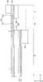
도 1은 본 발명의 실시예들에 따른 표시 장치를 나타내는 전개도이다.
도 2는 도 1의 표시 장치가 전개된 형상의 일 예를 나타내는 단면도이다.
도 3은 도 1의 표시 장치가 벤딩된 형상의 일 예를 나타내는 단면도이다.
도 4는 도 2의 표시 장치의 "C" 영역을 확대 도시한 일 예를 나타내는 단면도이다.
도 5a는 도 2의 표시 장치의 "D" 영역을 확대 도시한 일 예를 나타내는 단면도이다.
도 5b는 도 2의 표시 장치의 "D" 영역을 확대 도시한 다른 예를 나타내는 단면도이다.
도 6은 도 1의 표시 장치의 "A" 영역을 확대 도시한 일 예를 나타내는 평면도이다.
도 7은 도 6의 벤딩 영역에서 I-I'라인을 따라 절단한 단면도이다.
도 8 내지 도 12는 도 1의 표시 장치의 "A" 영역을 확대 도시한 예들을 나타내는 평면도들이다.
도 13 내지 도 18은 도 1의 표시 장치의 "B" 영역을 확대 도시한 예들을 나타내는 평면도들이다.
도 19 및 도 20은 도 1의 표시 장치의 효과를 설명하기 위한 도면들이다.1 is a development view showing a display device according to embodiments of the present invention.
Fig. 2 is a sectional view showing an example of a shape in which the display device of Fig. 1 is developed. Fig.
Fig. 3 is a cross-sectional view showing an example of a bent shape of the display device of Fig. 1;
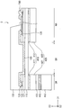
Fig. 4 is a cross-sectional view showing an example in which the "C" area of the display device of Fig. 2 is enlarged.
5A is a cross-sectional view showing an example in which the "D" region of the display device of Fig. 2 is enlarged.
5B is a cross-sectional view showing another example in which the "D" area of the display device of Fig. 2 is enlarged.
Fig. 6 is a plan view showing an example in which the "A" area of the display device of Fig. 1 is enlarged.
7 is a cross-sectional view taken along line I-I 'in the bending region of FIG.
Figs. 8 to 12 are plan views showing examples in which the "A" area of the display device of Fig. 1 is enlarged.
Figs. 13 to 18 are plan views showing examples of enlarging the "B" area of the display device of Fig.
19 and 20 are views for explaining the effect of the display device of FIG.
이하, 첨부한 도면들을 참조하여, 본 발명의 실시예들을 보다 상세하게 설명하고자 한다. 도면상의 동일한 구성 요소에 대해서는 동일하거나 유사한 참조 부호를 사용한다.Hereinafter, embodiments of the present invention will be described in detail with reference to the accompanying drawings. The same or similar reference numerals are used for the same components in the drawings.
도 1은 본 발명의 실시예들에 따른 표시 장치를 나타내는 전개도이다. 도 2는 도 1의 표시 장치가 전개된 형상의 일 예를 나타내는 단면도이다. 도 3은 도 1의 표시 장치가 벤딩된 형상의 일 예를 나타내는 단면도이다.1 is a development view showing a display device according to embodiments of the present invention. Fig. 2 is a sectional view showing an example of a shape in which the display device of Fig. 1 is developed. Fig. Fig. 3 is a cross-sectional view showing an example of a bent shape of the display device of Fig. 1;
도 1 내지 도 3을 참조하면, 표시 장치(1000)는 표시 패널(100), 구동 회로(300), 및, 하부 구조물을 포함할 수 있다.1 to 3, a
도 1에 도시된 바와 같이, 표시 패널(100)은 기판(110) 상에 복수의 화소(PX)들을 포함할 수 있다. 기판(110)은 표시 영역(DR), 벤딩 영역(BR), 및 패드 영역(NR)을 포함할 수 있다. 표시 영역(DR)은 액티브 영역(AA) 및 외곽 영역(OA)을 포함할 수 있다. 표시 영역(DR)의 액티브 영역(AA)에는 복수의 화소(PX)들이 배치될 수 있다. 일 실시예에서, 화소(PX)들은 유기 발광 소자(즉, 화소 구조물)를 포함하고, 매트릭스 형태로 액티브 영역(AA)에 배치될 수 있다. 표시 영역(DR)의 외곽 영역(OA)에는 화소(PX)들에 대한 봉지(encapsulation) 구조, 등이 형성될 수 있다. 벤딩 영역(BR)은 표시 영역(DR)과 패드 영역(NR) 사이에 위치할 수 있다. 기판(110)의 벤딩 영역(BR)은 벤딩될 수 있다. 일 실시예에서, 기판(110)은 비표시 영역이 사용자에게 시인되지 않도록 벤딩 영역(BR)에서 제2 방향(D2)을 축으로 화소 구조물(140)들이 바깥쪽을 향하도록 벤딩될 수 있다. 패드 영역(NR)은 표시 영역(DR)으로부터 이격되고, 구동 회로(300)와 같은 외부 장치들을 연결하기 위한 구조(예를 들어, 패드 배선(190), 등)을 포함할 수 있다. 이에 따라, 화소(PX)들은 구동 신호 또는 전원 전압을 제공받아 구동될 수 있다.As shown in FIG. 1, the
구동 회로(300)는 연결 배선(180) 및 패드 배선(190)들을 통해 화소(PX)들에 구동 신호를 제공할 수 있다. 여기서, 구동 신호는 화소(PX)을 구동하기 위한 스캔 신호, 데이터 신호, 발광 제어 신호, 등을 포함할 수 있다. 일 실시예에서, 구동 회로(300)는 COP(Chip On Plastic) 방식을 통해 기판(110)의 패드 영역(NR)에 직접 실장될 수 있다. 예를 들어, 구동 회로(300)는 이방 전도성 필름(Anisotropic Conductivity Films; ACF)을 사용하여 패드 배선(190) 상에 실장될 수 있다.The driving
연결 배선(180)은 구동 회로(300)와 화소(PX) (또는 화소 구조물)을 전기적으로 연결할 수 있다. 연결 배선(180)은 벤딩 영역(BR) 및/또는 패드 영역(NR)에서 노치(notch)들을 포함할 수 있다. 즉, 연결 배선(180)은 벤딩 영역(BR) 및/또는 패드 영역(NR)에 노치들을 형성함으로써 배선의 직선 부분의 길이를 줄이고, 제조 공정 중 벤딩 영역(BR) 또는 패드 영역(NR)에서 발생되는 인접한 배선들 사이의 단락을 방지할 수 있다.The
일 실시예에서, 연결 배선(180)들 각각은 벤딩 영역(BR) 및/또는 패드 영역(NR) 상에서 제1 측면에 제1 노치들을 포함하고, 제1 측면과 반대되는 제2 측면에 제2 노치들을 포함할 수 있다. 또한, 연결 배선(180)은 벤딩 영역(BR) 상에서 홀들을 포함할 수 있다. 예를 들어, 연결 배선(180)의 홀들은 연결 배선(180)을 수직 방향(즉, 제3 방향(D3))으로 관통할 수 있다. 연결 배선(180)은 인접한 제1 노치들 사이의 간격 및 인접한 제2 노치들 사이의 간격이 인접한 연결 배선(180)들 사이의 거리보다 짧게 형성함으로써 제조 공정 중 벤딩 영역(BR)에서 발생되는 인접한 배선들 사이의 단락을 방지할 수 있다. 다만, 벤딩 영역(BR) 및/또는 패드 영역(NR) 상에서 형성된 연결 배선(180)의 노치의 형상 및 배치에 대해서는 도 6 내지 도 12를 참조하여 자세히 설명하기로 한다.In one embodiment, each of the interconnecting
일 실시예에서, 패드 배선(190)들 각각은 패드 영역(NR) 상에서 제1 측면에 형성된 제3 노치들 및 제1 측면과 반대되는 제2 측면에 형성된 제4 노치들을 포함할 수 있다. 패드 배선(190)은 인접한 제3 노치들 사이의 간격 또는 인접한 제4 노치들 사이의 간격이 인접한 패드 배선(190)들 사이의 거리보다 짧게 형성함으로써 제조 공정 중 패드 영역(NR)에서 발생되는 인접한 배선들 사이의 단락을 방지할 수 있다. 다만, 패드 배선(190)의 노치의 형상 및 배치에 대해서는 도 13 내지 도 18를 참조하여 자세히 설명하기로 한다.In one embodiment, each of the
도 2에 도시된 바와 같이, 표시 장치(1000)는 표시 패널(100)의 하부에 하부 구조물을 포함할 수 있다. 하부 구조물은 제1 하부 접착층(410), 하부 보호 필름(420), 제2 하부 접착층(430), 방열판(440), 및 제3 하부 접착층(450)을 포함할 수 있다.As shown in FIG. 2, the
하부 보호 필름(420)은 제1 하부 보호 필름 패턴(421) 및 제2 하부 보호 필름 패턴(422)을 포함할 수 있다. 제1 하부 보호 필름 패턴(421)은 표시 영역(DR) 하부에 배치되고, 제2 하부 보호 필름 패턴(422)은 패드 영역(NR)에 하부에 배치될 수 있다. 이에 따라, 벤딩 영역(BR)에 대응하는 표시 패널(100)의 저면은 노출될 수 있다. 하부 보호 필름(420)은 폴리에틸렌 테레프탈레이트(polyethylene terephthalate PET), 폴리에틸렌 나프탈렌(polyethylene naphthalene PEN), 폴리프로필렌(polypropylene PP), 등을 포함할 수 있다.The lower
또한, 하부 보호 필름(420)과 표시 패널(100)을 접착시키기 위해 하부 보호 필름(420)과 표시 패널(100) 사이에 제1 하부 접착층(410)이 개재될 수 있다. 제1 하부 접착층(410)은 제1 하부 보호 필름 패턴(421)과 중첩되는 제1 하부 접착층 패턴(411) 및 제2 하부 보호 필름 패턴(422)과 중첩되는 제2 하부 접착층 패턴(412)을 포함할 수 있다. 제1 하부 접착층(410)은 표시 패널(100)의 저면에 접촉될 수 있다. 제1 하부 접착층(410)은 아크릴 계열 접착제, 실리콘 계열 접착제, 우레탄 계열 접착제, 등을 포함할 수 있다.The first lower
하부 보호 필름(420)의 저면 상에는 방열판(440)이 배치될 수 있고, 하부 보호 필름(420)과 방열판(440)을 접착하기 위해 하부 보호 필름(420)과 방열판(440) 사이에 제2 하부 접착층(430)이 개재될 수 있다. 방열판(440)이 표시 패널(100)의 저면 상에 배치됨으로써, 표시 패널(100)에서 발생하는 열을 방출시킬 수 있다. 표시 패널(100)에서 발생하는 열을 방출시키지 않을 경우, 표시 패널(100)에 포함된 화소(PX)들의 성능을 저감시키고, 수명을 단축시킬 수 있다. 방열판(440)은 열전도도가 높은 물질을 포함할 수 있다.A
도 3에 개시된 바와 같이, 벤딩 영역(BR)이 벤딩됨으로써, 패드 영역(NR)이 표시 장치(1000)의 저면에 위치할 수 있다. 일 실시예에서, 벤딩 영역(BR)은 제2 방향(D2)을 축으로 벤딩될 수 있고, 제2 하부 보호 필름 패턴(422)은 방열판(440)의 저면 상에 배치될 수 있다. 벤딩 영역(BR)이 벤딩된 후, 제2 하부 보호 필름 패턴(422)과 방열판(440) 사이에 제3 하부 접착층(450)이 개재될 수 있다. 이러한 경우, 제3 하부 접착층(450)에 의해 제2 하부 보호 필름 패턴(422)과 방열판(440)이 고정될 수 있다. 또한, 제3 하부 접착층(450)은 충격을 흡수하는 역할을 할 수 있다. 예를 들면, 제3 하부 접착층(450)은 우레탄, 고무 등을 포함할 수 있다.As shown in Fig. 3, the bending region BR is bent, so that the pad region NR can be positioned on the bottom surface of the
도 4는 도 2의 표시 장치의 "C" 영역을 확대 도시한 일 예를 나타내는 단면도이다. 도 5a는 도 2의 표시 장치의 "D" 영역을 확대 도시한 일 예를 나타내는 단면도이다.Fig. 4 is a cross-sectional view showing an example in which the "C" area of the display device of Fig. 2 is enlarged. 5A is a cross-sectional view showing an example in which the "D" region of the display device of Fig. 2 is enlarged.
도 4 및 도 5a를 참조하면, 표시 패널(100)은 기판(110), 반도체 소자(120), 제1 도전 패턴(128), 제2 도전 패턴(129), 평탄화층(130), 화소 구조물(140), 화소 정의막(150), 박막 봉지 구조물(170), 및 연결 배선들(180)을 포함할 수 있다. 표시 패널(100)은 플렉서블한 기판(110) 및 박막 봉지 구조물(170)을 포함함으로써, 플렉서블 표시 장치가 구현될 수 있다.4 and 5A, the
도 4에 도시된 바와 같이, 기판(110)은 연성을 갖는 투명 수지 기판으로 형성될 수 있다. 기판(110)으로 이용될 수 있는 투명 수지 기판의 예로는 폴리이미드 기판을 들 수 있다. 폴리이미드 기판은 제1 폴리이미드층, 제1 배리어층, 제2 폴리이미드층, 제2 배리어층 등으로 구성될 수 있다. 폴리이미드 기판이 얇고 연성을 갖는 경우, 폴리이미드 기판은 반도체 소자(120) 및 발광 구조물(140) (예를 들어, 하부 전극(141), 발광층(142), 상부 전극(143) 등)의 형성을 지원하기 위해 단단한 유리 상에 형성될 수 있다. 즉, 기판(110)은 유리 기판 상에 제1 폴리이미드층, 제1 배리어층, 제2 폴리이미드층 및 제2 배리어층이 적층된 구성을 가질 수 있다. 예를 들면, 제2 배리어층 상에 절연층(예를 들어, 버퍼층)을 배치한 후, 절연층 상에 반도체 소자(120) 및 발광 구조물(140)을 형성할 수 있다. 이러한 반도체 소자(120) 및 발광 구조물(140)의 형성 후, 유리 기판은 제거될 수 있다.As shown in FIG. 4, the
기판(110) 상에는 버퍼층(도시되지 않음)이 배치될 수 있다. 버퍼층은 기판(110) 상에 전체적으로 배치될 수 있다. 버퍼층은 기판(110)으로부터 금속 원자들이나 불순물들이 확산되는 현상을 방지할 수 있으며, 액티브층(121)을 형성하기 위한 결정화 공정 동안 열의 전달 속도를 조절하여 실질적으로 균일한 액티브층(121)을 수득하게 할 수 있다. 또한, 버퍼층은 기판(110)의 표면이 균일하지 않을 경우, 기판(110)의 표면의 평탄도를 향상시키는 역할을 수행할 수 있다. 기판(110)의 유형에 따라 기판(110) 상에 두 개 이상의 버퍼층이 제공될 수 있거나 버퍼층이 배치되지 않을 수 있다. 버퍼층은 실리콘 화합물, 금속 산화물 등을 포함할 수 있다.A buffer layer (not shown) may be disposed on the
기판(110) 상에 반도체 소자(120)가 배치될 수 있다. 반도체 소자(120)는 액티브층(121), 게이트 절연층(122), 게이트 전극(123), 층간 절연층(124), 소스 전극(125), 및 드레인 전극(126)을 포함할 수 있다.The
액티브층(121)은 기판(110) 상에 배치될 수 있다. 액티브층(121)은 산화물 반도체, 무기물 반도체(예를 들면, 아몰퍼스 실리콘(amorphous silicon), 폴리 실리콘(poly silicon)) 또는 유기물 반도체 등을 포함할 수 있다.The
액티브층(121) 상에는 게이트 절연층(122)이 배치될 수 있다. 게이트 절연층(122)은 액티브층(121)을 덮을 수 있으며, 기판(110) 상에 배치될 수 있다. 예를 들면, 게이트 절연층(122)은 액티브층(121)을 충분히 덮을 수 있으며, 액티브층(121)의 주위에 단차를 생성시키지 않고 실질적으로 평탄한 상면을 가질 수 있다. 선택적으로, 게이트 절연층(122)은 기판(110) 상에서 액티브층(121)을 덮으며, 균일한 두께로 액티브층(121)의 프로파일을 따라 배치될 수 있다. 예시적인 실시예들에 있어서, 게이트 절연층(122)은 벤딩 영역(BR) 및 패드 영역(NR)의 일부에 위치하는 기판(110)의 상면을 노출시킬 수 있다. 게이트 절연층(122)은 실리콘 화합물, 금속 산화물 등을 포함할 수 있다.A
게이트 전극(123)은 게이트 절연층(122) 중에서 하부에 액티브층(121)이 위치하는 부분 상에 배치될 수 있다. 게이트 전극(123)은 금속, 합금, 금속 질화물, 도전성 금속 산화물, 투명 도전성 물질 등을 포함할 수 있다.The
게이트 전극(123) 상에는 층간 절연층(124)이 배치될 수 있다. 층간 절연층(124)은 게이트 전극(123)을 덮을 수 있으며, 게이트 절연층(122) 상에서 배치될 수 있다. 예를 들면, 층간 절연층(124)은 게이트 절연층(122) 상에서 게이트 전극(123)을 충분히 덮을 수 있으며, 게이트 전극(123)의 주위에 단차를 생성시키지 않고 실질적으로 평탄한 상면을 가질 수 있다. 선택적으로, 층간 절연층(124)은 게이트 절연층(122) 상에서 게이트 전극(123)을 덮으며, 균일한 두께로 게이트 전극(123)의 프로파일을 따라 배치될 수 있다. 예시적인 실시예들에 있어서, 층간 절연층(124)은 벤딩 영역(BR) 및 패드 영역(NR)의 일부에 위치하는 기판(110)의 상면을 노출시킬 수 있다. 층간 절연층(124)은 실리콘 화합물, 금속 산화물 등을 포함할 수 있다.An interlayer insulating
층간 절연층(124) 상에는 소스 전극(125) 및 드레인 전극(126)이 배치될 수 있다. 소스 전극(125) 및 드레인 전극(126) 각각은 게이트 절연층(122) 및 층간 절연층(124)의 일부를 관통하여 액티브층(121)의 일측 및 타측에 각각 접속될 수 있다. 소스 전극(125) 및 드레인 전극(126)은 각기 금속, 합금, 금속 질화물, 도전성 금속 산화물, 투명 도전성 물질 등을 포함할 수 있다. 이들은 단독으로 또는 서로 조합되어 사용될 수 있다. 다른 예시적인 실시예들에 있어서, 소스 전극(125) 및 드레인 전극(126)은 복수의 층들으로 구성될 수도 있다.A
도 5a에 도시된 바와 같이, 구동 회로 또는 외부 장치는 데이터 신호, 스캔 신호, 발광 제어 신호, 전원 전압 등을 패드 배선(190), 제2 도전 패턴(129), 연결 배선(180), 및 제1 도전 패턴(128)을 통해 화소들에 제공할 수 있다.5A, a driving circuit or an external device supplies a data signal, a scan signal, a light emission control signal, a power supply voltage, and the like to the
제1 도전 패턴(128)은 표시 영역(DR)의 가장자리(예를 들어, 도 1의 외곽 영역(OA))에서 게이트 절연층(122) 상에 배치될 수 있다. 제1 도전 패턴(128)은 복수의 배선들 중 하나일 수 있다. 예를 들면, 제1 도전 패턴(128)은 데이터 신호 배선, 스캔 신호 배선, 발광 제어 신호 배선, 전원 전압 배선 등을 포함할 수 있다.The first
제2 도전 패턴(129)은 게이트 절연층(122) 상의 패드 영역(NR)에 배치될 수 있다. 제2 도전 패턴(129)은 패드 배선(190)과 전기적으로 연결될 수 있다.The second
연결 배선(180)은 벤딩 영역(BR)에서 기판(110) 상에 배치되고, 표시 영역(DR)의 가장자리 및 패드 영역(NR)의 일부에서 층간 절연층(124) 상에 배치될 수 있다. 연결 배선(180)은 표시 영역(DR)의 가장자리에 위치하는 층간 절연층(124)의 일 부분을 제거하여 형성된 콘택홀을 통해 제1 도전 패턴(128)에 접속될 수 있고, 패드 영역(NR)에 위치하는 층간 절연층(124)의 일 부분을 제거하여 형성된 콘택홀을 통해 제2 도전 패턴(129)에 접속될 수 있다. 연결 배선(180) 상에 평탄화층(130)이 배치될 수 있다.The
패드 배선(190)은 패드 영역(NR)에서 층간 절연층(124) 상에 배치될 수 있다. 패드 배선(190)은 패드 영역(NR)에 위치하는 층간 절연층(124)의 일 부분을 제거하여 형성된 콘택홀을 통해 제2 도전 패턴(129)에 접속될 수 있다. The
일 실시예에서, 제1 도전 패턴(128), 제2 도전 패턴(129) 및 게이트 전극(123)은 동일한 물질을 사용하여 동시에 형성될 수 있다. 또한, 연결 배선(180) 및 패드 배선(190)은 소스 및 드레인 전극들(125, 126)과 동일한 물질을 사용하여 동시에 형성될 수 있다.In one embodiment, the first
일 실시예에서, 연결 배선(180) 및 패드 배선(190)은 알루미늄을 포함하는 금속막이 적층된 다중막으로 형성될 수 있다. 예를 들어, 연결 배선(180) 및 패드 배선(190)은 티타늄/알루미늄/티타늄(Ti/Al/Ti)의 3중막으로 형성될 수 있다. 이 경우, 최상층에 배치된 티타늄(Ti)은 식각하고 세정하는 과정에서 손상될 수 있다. 연결 배선(180) 및 패드 배선(190)의 파티클(예를 들어, 티타늄(Ti) 파티클)에 의해 인접한 연결 배선(180)들 사이 및 패드 배선(190)들 사이가 단락될 수 있으므로, 직선으로 긴 파티클이 생기지 않도록 연결 배선(180) 및 패드 배선(190)은 노치들을 포함할 수 있다. 또한, 연결 배선(180)은 벤딩 영역(BR)에서 유연한 특성을 가질 수 있도록 벤딩 영역(BR)의 상부에서 홀들을 포함할 수 있다.In one embodiment, the
이에 따라, 구동 회로 또는 외부 장치는 패드 배선(190)과 전기적으로 연결될 수 있고, 구동 회로 또는 외부 장치는 데이터 신호, 스캔 신호, 발광 신호, 전원 전압 등을 패드 배선(190), 제2 도전 패턴(129), 연결 배선(180) 및 제1 도전 패턴(128)을 통해 화소들에 제공할 수 있다.Accordingly, the driving circuit or the external device can be electrically connected to the
다시 도 4에서, 소스 전극(125) 및 드레인 전극(126) 상에 평탄화층(130)이 배치될 수 있다. 평탄화층(130)은 소스 전극(125) 및 드레인 전극(126)을 덮을 수 있다. 일 실시예에서, 평탄화층(130)은 소스 전극(125) 및 드레인 전극(126)을 충분히 덮도록 상대적으로 두꺼운 두께로 배치될 수 있고, 이러한 경우, 평탄화층(130)은 실질적으로 평탄한 상면을 가질 수 있으며, 이와 같은 평탄화층(130)의 평탄한 상면을 구현하기 위하여 평탄화층(130)에 대해 평탄화 공정이 추가될 수 있다. 선택적으로, 평탄화층(130)은 소스 전극(125) 및 드레인 전극(126)을 덮으며, 균일한 두께로 소스 전극(125) 및 드레인 전극(126)의 프로파일을 따라 배치될 수 있다. 평탄화층(130)은 유기 물질 또는 무기 물질로 이루어질 수 있다.Referring again to FIG. 4, the
하부 전극(141)은 평탄화층(130) 상에 배치될 수 있다. 하부 전극(141)은 평탄화층(130)의 일부를 관통하여 드레인 전극(126)에 접속될 수 있다. 또한, 하부 전극(141)은 반도체 소자(120)와 전기적으로 연결될 수 있다. 하부 전극(141)은 금속, 합금, 금속 질화물, 도전성 금속 산화물, 투명 도전성 물질 등을 포함할 수 있다. 이들은 단독으로 또는 서로 조합되어 사용될 수 있다. 일 실시예에서, 하부 전극(141)은 복수의 층들로 구성될 수도 있다.The
화소 정의막(150)은 평탄화층(130) 상에 배치될 수 있고, 하부 전극(141)의 일부를 노출시킬 수 있다. 화소 정의막(150)에 의해 하부 전극(141)이 노출된 부분에 발광층(142)이 배치될 수 있다. 일 실시예에서, 화소 정의막(150)은 벤딩 영역(BR) 및 패드 영역(NR)을 노출시킬 수 있다. 화소 정의막(150)은 유기 물질 또는 무기 물질로 이루어질 수 있다.The
발광층(142)은 적어도 일부가 노출된 하부 전극(141) 상에 배치될 수 있다. 발광층(142)은 서브 화소들에 따라 상이한 색광들(즉, 적색광, 녹색광, 청색광 등)을 방출시킬 수 있는 발광 물질들 중 적어도 하나를 사용하여 형성될 수 있다. 이와는 달리, 발광층(142)은 적색광, 녹색광, 청색광 등의 다른 색광들을 발생시킬 수 있는 복수의 발광 물질들을 적층하여 전체적으로 백색광을 방출할 수 있다. 이러한 경우, 발광층(142) 상에 컬러 필터가 배치될 수 있다.The
상부 전극(143)은 화소 정의막(150) 및 발광층(142) 상에 배치될 수 있다. 상부 전극(143)은 금속, 합금, 금속 질화물, 도전성 금속 산화물, 투명 도전성 물질 등을 포함할 수 있다.The
박막 봉지 구조물(170)은 상부 전극(143) 상에 배치될 수 있다. 박막 봉지 구조물(170)은 제1 봉지층(171), 제2 봉지층(172) 및 제3 봉지층(173)을 포함할 수 있다. 예를 들면, 상부 전극(143) 상에 제1 봉지층(171)이 배치될 수 있다. 제1 봉지층(171)은 상부 전극(143)을 덮으며, 균일한 두께로 상부 전극(143)의 프로 파일을 따라 배치될 수 있다. 제1 봉지층(171)은 발광 구조물(140)이 수분, 산소 등의 침투로 인해 열화되는 것을 방지할 수 있다. 또한, 제1 봉지층(171)은 외부의 충격으로부터 발광 구조물(140)을 보호하는 기능도 수행할 수 있다. 제1 봉지층(171)은 무기 물질들을 포함할 수 있다. 제1 봉지층(171) 상에 제2 봉지층(172)이 배치될 수 있다. 제2 봉지층(172)은 표시 장치의 평탄도를 향상시킬 수 있으며, 발광 구조물(140)을 보호할 수 있다. 제2 봉지층(172) 유기 물질들을 포함할 수 있다. 제2 봉지층(172) 상에 제3 봉지층(173)이 배치될 수 있다. 제3 봉지층(173)은 제2 봉지층(172)을 덮으며, 균일한 두께로 제2 봉지층(172)의 프로 파일을 따라 배치될 수 있다. 제3 봉지층(173)은 제1 봉지층(171) 및 제2 봉지층(172)과 발광 구조물(140)이 수분, 산소 등의 침투로 인해 열화되는 것을 방지할 수 있다. 또한, 제3 봉지층(173)은 외부의 충격으로부터 제1 봉지층(171) 및 제2 봉지층(172)과 발광 구조물(140)을 보호하는 기능도 수행할 수 있다. 제3 봉지층(173)은 무기 물질들을 포함할 수 있다.The thin
비록, 도 4에서는 반도체 소자(120)가 상부 게이트 구조를 갖는 것으로 설명하였으나, 본 발명의 구성이 이에 한정되지 않는다. 예를 들면, 반도체 소자(120)는 하부 게이트 구조를 가질 수 있다.Although the
또한, 도 4에서는 박막 봉지 구조물이 3층 구조인 것으로 도시하였으나, 이에 한정되지 않는다. 예를 들어, 박막 봉지 구조물은 제1 내지 제5 봉지층들로 적층된 5층 구조 또는 제1 내지 제7 봉지층들로 적층된 7층 구조로 구성될 수도 있다.4, the thin film encapsulation structure has a three-layer structure, but the present invention is not limited thereto. For example, the thin film encapsulation structure may be a five-layer structure stacked with the first to fifth encapsulation layers or a seven-layer structure stacked with the first to seventh encapsulation layers.
도 5b는 도 2의 표시 장치의 "D" 영역을 확대 도시한 다른 예를 나타내는 단면도이다.5B is a cross-sectional view showing another example in which the "D" area of the display device of Fig. 2 is enlarged.
도 4 및 도 5b를 참조하면, 구동 회로 또는 외부 장치는 데이터 신호, 스캔 신호, 발광 신호, 전원 전압 등을 제2 도전 패턴(129), 연결 배선(180) 및 제1 도전 패턴(128)을 통해 화소들에 제공할 수 있다. 다만, 본 실시예에 따른 표시 장치의 연결 구조는 벤딩 영역(BR)에서 기판(110) 및 연결 배선(180) 사이에 제1 절연층(127)이 추가된 것을 제외하면, 도 5a의 표시 장치의 연결 구조와 실질적으로 동일하므로, 동일 또는 유사한 구성 요소에 대해서는 동일한 참조 번호를 사용하고, 중복되는 설명은 생략하기로 한다.Referring to FIGS. 4 and 5B, the driving circuit or the external device may include a second
제1 절연층(127)은 벤딩 영역(BR)에서 기판(110)의 상부에 배치되고, 제1 도전 패턴(128)은 벤딩 영역(BR)에서 제1 절연층(127) 상에 배치될 수 있다.The first insulating
일 실시예에서, 제1 절연층(127)은 실질적으로 평탄한 상면을 가질 수 있으며, 이와 같은 제1 절연층(127)의 평탄한 상면을 구현하기 위하여 제1 절연층(127)에 대해 평탄화 공정이 추가될 수 있다. 예를 들어, 연결 배선(180)이 끊어지지 않게 하기 위해 벤딩 영역(BR)에서 중립면이 연결 배선(180)이 배치된 부분에 위치하도록 제1 절연층(127)의 두께가 조정될 수 있다. 이에 따라, 연결 배선(180)의 내구성을 향상시킬 수 있다.In one embodiment, the first insulating
다른 실시예에서, 제1 절연층(127)은 상면의 적어도 일부에 요철면을 가질 수 있다. 이에 따라, 제1 절연층(127) 상에 위치하는 연결 배선(180)은 그 상면 및/또는 하면이 제1 절연층(127)의 요철면에 대응하는 형상을 가질 수 있다. 기판(110)이 벤딩 영역(BR)에서 벤딩됨에 따라, 벤딩 영역(BR)에서 연결 배선(180)에 인장 스트레스가 인가될 수 있으므로, 연결 배선(180)의 상면 및/또는 하면이 제1 절연층(127)의 요철면에 대응하는 형상을 갖도록 함으로써, 연결 배선(180)에 인가되는 인장 스트레스의 양을 최소화할 수 있다. 즉, 벤딩 과정에서 발생할 수 있는 인장 스트레스를 강도가 낮은 제1 절연층(127)의 형상의 변형을 통해 줄일 수 있으며, 이때 적어도 벤딩 전에 요철 형상을 갖는 연결 배선(180)의 형상이 벤딩에 의해 변형된 절연층(127)의 형상에 대응하도록 변형되도록 함으로써, 연결 배선(180)에서 단락이 발생하는 것을 방지할 수 있다.In another embodiment, the first insulating
비록, 도 5a 및 도 5b에서는 제1 도전 패턴(128) 및 제2 도전 패턴(129)을 통해 화소와 외부 장치들이 전기적으로 연결되는 것으로 도시되었으나, 이에 한정되지 않는다. 예를 들어, 외부 장치들은 연결 배선과 직접적으로 접촉되는 패드 배선을 통해 연결 배선과 전기적으로 연결될 수 있다. 또한, 연결 배선들 각각은 스캔 신호 배선, 데이터 신호 배선, 발광 제어 신호 배선, 및 전원 전압 배선 중 하나와 직접적으로 연결될 수 있다.Although FIGS. 5A and 5B illustrate that the pixel and the external device are electrically connected through the first
비록, 도 5a 및 도 5b에서는 벤딩 영역(BR) 및 패드 영역(NR)에서 평탄화층(130)이 연결 배선(180)을 덮는 것으로 도시되었으나, 이에 한정되지 않는다. 연결 배선(180)은 노출되거나, 연결 배선(180)은 평탄화층(130), 화소 정의막(150), 및 벤딩 보호층(미도시) 중 적어도 하나에 의해 덮일 수 있다. 예를 들어, 벤딩 영역(BR) 및 패드 영역(NR)의 일부에서 평탄화 층(180) 상부에 벤딩 보호층(미도시)을 더 포함할 수 있다. 즉, 벤딩 영역(BR)에서 중립면이 연결 배선(180)들이 배치된 부분에 위치하도록 벤딩 보호층의 두께가 결정될 수 있다. 예를 들면, 벤딩 영역(BR)의 중립면이 연결 배선(180)들이 배치된 부분에 위치하는 경우, 벤딩 영역(BR)이 벤딩됨에 따라 연결 배선(180)들이 받는 벤딩 부하가 감소되므로, 연결 배선(180)들은 끊어지지 않을 수 있다.Although the
비록, 도 5a 및 도 5b에서는 연결 배선(180)이 벤딩 영역(BR) 및/또는 패드 영역(NR)에서 노치를 포함하는 것으로 설명하였으나, 연결 배선(180)은 표시 영역(DR)의 일부를 포함하는 연결 배선(180)의 전반에서 노치를 포함할 수 있다. 예를 들어, 연결 배선(180)은 표시 영역(DR) 및 패드 영역(NR)에서는 노치만을 포함하고, 벤딩 영역(BR)에서는 홀 및 노치를 모두 포함할 수 있다.5A and 5B, the
도 6은 도 1의 표시 장치의 "A" 영역을 확대 도시한 일 예를 나타내는 평면도이다. 도 7은 도 6의 벤딩 영역에서 I-I'라인을 따라 절단한 단면도이다.Fig. 6 is a plan view showing an example in which the "A" area of the display device of Fig. 1 is enlarged. 7 is a cross-sectional view taken along line I-I 'in the bending region of FIG.
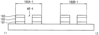
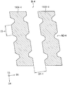
도 6 및 도 7을 참조하면, 연결 배선들(180A-1, 180B-1, 등) 각각은 벤딩 영역의 적어도 일부(A-1)에서 홀(HL-1)들 및 노치(NT-1)들을 포함함으로써 제조 공정 중 벤딩 영역에서 발생되는 인접한 배선들 사이의 단락을 방지할 수 있다.6 and 7, each of the interconnecting interconnects 180A-1, 180B-1, etc. has holes HL-1 and notches NT-1 in at least a portion A- It is possible to prevent a short circuit between adjacent wirings generated in the bending area during the manufacturing process.
도 7에 도시된 바와 같이, 연결 배선들(180A-1, 180B-1) 각각은 제1 금속층(181), 제2 금속층(182), 및 제3 금속층(183)을 포함할 수 있다. 예를 들어, 제1 금속층(181), 제2 금속층(182), 및 제3 금속층(183)은 각각 티타늄/알루미늄/티타늄 (Ti/Al/Ti) 또는 또는 몰리브덴/알루미늄/몰리브덴 (Mo/Al/Mo)에 대응할 수 있다. 연결 배선들(180A-1, 180B-1)을 Ti/Al/Ti 또는 Mo/Al/Mo의 3층으로 구성하는 경우, 정밀도가 높은 건식 식각(dry etch)을 이용하여 형성할 수 있으므로 배선들 사이의 간격을 좁게 형성할 수 있다. 따라서, 좁은 공간에 많은 배선들을 배치할 수 있어 해상도가 높은 표시 장치에 적합할 수 있다.7, each of the interconnecting
이 경우, 티타늄(Ti) 또는 몰리브덴(Mo)을 포함하는 제3 금속층(183)은 식각 공정, 세정 공정, 또는 그 밖의 충격으로 인해 제조 공정 중에 쉽게 손상될 수 있다. 예를 들어, COP 방식으로 구동 회로를 실장하는 경우, 컨텍(contact) 들뜸 방지를 위해 벤딩 영역(BR)에서 연결 배선들(180A-1, 180B-1)은 캐핑(capping) 없이 노출될 수 있다. 이에 따라, 연결 배선들(180A-1, 180B-1)의 파티클(예를 들어, 티타늄(Ti) 파티클)에 의해 인접한 연결 배선들(180A-1, 180B-1) 사이가 단락될 수 있으므로, 직선으로 긴 파티클이 생기지 않도록 연결 배선들(180A-1, 180B-1) 각각은 노치(NT-1)들을 포함할 수 있다.In this case, the
도 6에 도시된 바와 같이, 벤딩 영역(BR)에서, 연결 배선들(180A-1, 180B-1) 각각은 제1 측면 및 제1 측면에 반대되는 제2 측면에 노치(NT-1)들을 포함할 수 있다. 일 실시예에서, 노치(NT-1)들은 연결 배선이 연장된 제1 방향(D1)에 대해 일정한 간격으로 형성되고, 인접한 두 개의 노치(NT-1)들 사이의 제1 거리(D1-1)는 인접한 두 개의 연결 배선들(180A-1, 180B-1) 사이의 제2 거리(D2-1)보다 작을 수 있다. 여기서, 제1 거리(D1-1)는 노치(NT-1)에 의해 형성되는 연결 배선의 직선 부분의 길이를 나타낸다. 제2 거리(D2-1)는 인접한 두 개의 연결 배선들(180A-1, 180B-1) 사이의 최단 거리를 나타낸다. 즉, 벤딩 영역(BR)에서, 연결 배선들(180A-1, 180B-1) 간의 제2 거리(D2-1)를 고려하여 노치(NT-1)들 사이의 제1 거리(D1-1)가 충분히 짧도록 노치(NT-1)들이 생성될 수 있다. 이에 따라, 벤딩 영역(BR)에서 제1 방향(D1)으로 연장된 연결 배선들(180A-1, 180B-1)에서 직선으로 연장된 형태가 되지 않도록 방지함으로써 긴 막대 모양의 파티클이 생성되지 않도록 방지될 수 있다.As shown in Fig. 6, in the bending region BR, each of the interconnecting
연결 배선들(180A-1, 180B-1) 각각은 벤딩 영역(BR)에서 유연한 특성을 가질 수 있도록 벤딩 영역(BR)의 상부에서 홀(HL-1)들을 포함할 수 있다. 홀(HL-1)들은 연결 배선을 수직 방향(즉, 제3 방향(D3))으로 관통하고, 제1 방향(D1)에 대해 일정한 간격으로 형성될 수 있다. 일 실시예에서, 홀(HL-1)들 각각의 제1 크기(S1)는 제2 거리(D2-1)보다 작을 수 있다. 여기서, 홀(HL-1)의 제1 크기(S1)는 평면 상에서 가장 긴 홀의 길이에 상응할 수 있다. 일 예에서, 홀(HL-1)들은 원형 모양을 갖고, 홀(HL-1)의 제1 크기(S1)는 직경에 상응할 수 있다. 다른 예에서, 홀(HL-1)들은 타원형 모양을 갖고, 홀(HL-1)의 제1 크기(S1)는 장직경에 상응할 수 있다. 또 다른 예에서, 홀(HL-1)들은 다각형 모양을 갖고, 홀(HL-1)의 제1 크기(S1)는 상기 다각형의 대각선들 중 가장 긴 하나의 길이에 상응할 수 있다. 이에 따라, 홀을 형성하는 과정에서 발생하는 파티클에 의해 발생될 수 있는 연결 배선들(180A-1, 180B-1)의 단락을 방지할 수 있다.Each of the interconnecting
비록, 도 7에서는 연결 배선들(180A-1, 180B-1) 각각은 티타늄/알루미늄/티타늄 (Ti/Al/Ti) 3층 구조를 갖는 것으로 도시하였으나, 이에 한정되지 않는다. 예를 들어, 연결 배선들 각각은 알루미늄(Al), 백금(Pt), 팔라듐(Pd), 은(Ag), 마그네슘(Mg), 금(Au), 니켈(Ni), 네오디뮴(Nd), 이리듐(Ir), 크롬(Cr), 리튬(Li), 칼슘(Ca), 몰리브덴(Mo), 티타늄(Ti), 텅스텐(W), 구리(Cu) 중 하나 이상의 물질로 단층 또는 다층으로 형성될 수 있다.Although each of the interconnecting
도 8 내지 도 12는 도 1의 표시 장치의 "A" 영역을 확대 도시한 예들을 나타내는 평면도들이다.Figs. 8 to 12 are plan views showing examples in which the "A" area of the display device of Fig. 1 is enlarged.
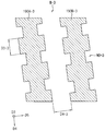
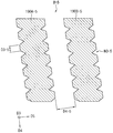
도 8 내지 도 12을 참조하면, 벤딩 영역의 상부에서 연결 배선들 각각은 연결 배선의 특성 및 배치에 따라 홀 및 노치들이 다양한 방법으로 형성될 수 있다.Referring to Figures 8-12, each of the interconnecting interconnects at the top of the bending region may be formed in a variety of ways, depending on the nature and placement of the interconnecting interconnects.
도 8에 도시된 바와 같이, 연결 배선들(180A-2, 180B-2) 각각은 벤딩 영역의 적어도 일부(A-2)에서 타원형 모양을 갖는 홀(HL-2)들 및 반원형 모양을 갖는 노치(NT-2)들을 포함할 수 있다. 노치(NT-2)들은 제1 방향(D1)에 대해 일정한 간격으로 형성되고, 인접한 두 개의 노치(NT-2)들 사이의 제1 거리(D1-2)는 인접한 두 개의 연결 배선들(180A-2, 180B-2) 사이의 제2 거리(D2-2)보다 작을 수 있다. 홀(HL-2)들은 연결 배선의 제2 방향(D2)의 중앙에 위치하며, 연결 배선을 수직 방향(즉, 제3 방향(D3))으로 관통하고, 제1 방향(D1)에 대해 일정한 간격으로 형성될 수 있다. 홀(HL-2)의 크기는 제2 거리(D2-1)보다 작을 수 있다.As shown in Fig. 8, each of the
일반적으로, 노치(NT-2)에 의해 연결 배선들(180A-2, 180B-2)의 배선폭(line width)이 작아지는 경우, 연결 배선들(180A-2, 180B-2)의 저항이 증가될 수 있다. 또한, 배선폭이 균일한 경우보다 불균일한 경우 상대적으로 연결 배선들(180A-2, 180B-2)의 저항이 증가될 수 있다. 따라서, 노치(NT-2)에 의해 감소하는 배선폭의 정도를 낮추면서도 홀(HL-2)과 노치(NT-2)에 따라 결정되는 배선폭의 균일한 정도를 높일 수 있도록, 노치(NT-2)는 반원형 모양을 갖고, 노치(NT-2)와 홀(HL-2)이 제1 방향(D1)을 따라 번갈아 배치되도록 형성할 수 있다. 이에 따라, 연결 배선들(180A-2, 180B-2)의 저항이 증가하지 않고 전기적 신호 전달의 효율성을 높일 수 있다.In general, when the line width of the interconnecting
도 9에 도시된 바와 같이, 연결 배선들(180A-3, 180B-3) 각각은 벤딩 영역의 적어도 일부(A-2)에서 타원형 모양을 갖는 홀(HL-3)들 및 직사각형 모양을 갖는 노치(NT-3)들을 포함할 수 있다. 노치(NT-3)들은 제1 방향(D1)에 대해 일정한 간격으로 형성되고, 인접한 두 개의 노치(NT-3)들 사이의 제1 거리(D1-3)는 인접한 두 개의 연결 배선들(180A-3, 180B-3) 사이의 제2 거리(D2-3)보다 작을 수 있다. 홀(HL-3)들은 연결 배선의 제2 방향(D2)의 중앙에 위치하며, 연결 배선을 수직 방향(즉, 제3 방향(D3))으로 관통하고, 제1 방향(D1)에 대해 일정한 간격으로 형성될 수 있다. 홀(HL-2)의 크기는 제2 거리(D2-1)보다 작을 수 있다.As shown in Fig. 9, each of the interconnecting
일반적으로, 노치(NT-3)가 홀(HL-3)에서 멀도록 형성함으로써 연결 배선들(180A-3, 180B-3)의 저항을 감소시킬 수 있다. 따라서, 연결 배선들(180A-3, 180B-3)은 벤딩 영역(BR) 상에서 제1 방향(D1)으로 연장되고, 홀(HL-3)들은 제1 방향(D1)과 직교하는 제2 방향(D2)에서 직사각형 모양을 갖는 노치(NT-3)들과 중첩되지 않도록 형성될 수 있다. 즉, 배선폭이 좁아지는 부분이 형성되지 않도록 노치(NT-3)와 홀(HL-3) 사이의 최소 거리를 확보함으로써 연결 배선들(180A-3, 180B-3)의 저항이 감소될 수 있다. 따라서, 노치(NT-3)에 의해 감소하는 배선폭의 정도를 낮추면서도 홀(HL-3)과 노치(NT-3)에 따라 결정되는 배선폭의 균일한 정도를 높일 수 있도록, 노치(NT-3)는 직사각형 모양을 갖고, 노치(NT-3)와 홀(HL-3)이 제1 방향(D1)을 따라 번갈아 배치되도록 형성할 수 있다. 이에 따라, 연결 배선들(180A-3, 180B-3)의 저항이 증가하지 않고 전기적 신호 전달의 효율성을 높일 수 있다.Generally, the resistance of the
도 10에 도시된 바와 같이, 연결 배선들(180A-4, 180B-4) 각각은 벤딩 영역의 적어도 일부(A-4)에서 타원형 모양을 갖는 홀(HL-4)들 및 사다리꼴 모양을 갖는 노치(NT-4)들을 포함할 수 있다. 노치(NT-4)들은 제1 방향(D1)에 대해 일정한 간격으로 형성되고, 인접한 두 개의 노치(NT-4)들 사이의 제1 거리(D1-4)는 인접한 두 개의 연결 배선들(180A-4, 180B-4) 사이의 제2 거리(D2-4)보다 작을 수 있다. 홀(HL-4)들은 연결 배선의 제2 방향(D2)의 중앙에 위치하며, 연결 배선을 수직 방향(즉, 제3 방향(D3))으로 관통하고, 제1 방향(D1)에 대해 일정한 간격으로 형성될 수 있다. 홀(HL-4)의 크기는 제2 거리(D2-4)보다 작을 수 있다.As shown in Fig. 10, each of the interconnecting
노치(NT-4)에 의해 감소하는 배선폭의 정도를 낮추면서도 홀(HL-4)과 노치(NT-4)에 따라 결정되는 배선폭의 균일한 정도를 높일 수 있도록, 노치(NT-4)는 사다리꼴 모양을 갖고, 노치(NT-4)와 홀(HL-4)이 제1 방향(D1)에서 번갈아 배치되도록 형성할 수 있다. 이와 같이, 벤딩 영역(BR)의 상부에서 연결 배선들(180A-4, 180B-4)에 노치(NT-4)들을 사다리꼴 모양으로 형성함으로써, 도 9의 직사각형 모양의 노치(NT-3)들을 포함하는 연결 배선들(180A-3, 180B-3)에 비해 배선폭의 균일도를 높일 수 있다. 또한, 연결 배선들(180A-4, 180B-4)은 벤딩 영역(BR) 상에서 제1 방향(D2)으로 연장되고, 홀(HL-4)들은 제1 방향(D1)과 직교하는 제2 방향(D2)에서 사다리꼴 모양을 갖는 노치(NT-4)들과 중첩되지 않도록 형성될 수 있다. The notches NT-4 and NT-4 are formed so as to increase the uniformity of the wiring width determined by the holes HL-4 and NT-4 while reducing the degree of the wiring width decreasing by the notch NT- May have a trapezoidal shape and the notches NT-4 and HL-4 may be alternately arranged in the first direction D1. By forming the notches NT-4 in a trapezoidal shape in the
도 11에 도시된 바와 같이, 연결 배선들(180A-5, 180B-5) 각각은 벤딩 영역의 적어도 일부(A-5)에서 타원형 모양을 갖는 홀(HL-5)들 및 삼각형 모양을 갖는 노치(NT-5)들을 포함할 수 있다. 노치(NT-5)들은 제1 방향(D1)에 대해 일정한 간격으로 형성되고, 인접한 두 개의 노치(NT-5)들 사이의 제1 거리(D1-5)는 인접한 두 개의 연결 배선들(180A-5, 180B-5) 사이의 제2 거리(D3-5)보다 작을 수 있다. 홀(HL-5)들은 연결 배선의 제2 방향(D2)의 중앙에 위치하며, 연결 배선을 수직 방향(즉, 제3 방향(D3))으로 관통하고, 제1 방향(D1)에 대해 일정한 간격으로 형성될 수 있다. 홀(HL-2)의 크기는 제2 거리(D2-1)보다 작을 수 있다.As shown in Fig. 11, each of the interconnecting
도 11에 도시된 연결 배선들(180A-5, 180B-5)은 도 6에 도시된 연결 배선들(180A-1, 180B-1)에 비해 상대적으로 짧은 간격으로 노치(NT-5)들이 형성되는 반면, 상대적으로 작의 크기의 노치(NT-5)를 포함할 수 있다. 예를 들어, 제2 방향(D2)에 대해 하나의 홀(HL-5)에 대응하여 2개의 노치(NT-5)들이 대응되도록 배치할 수 있다. 이 경우, 다른 실시예들에 비해 배선폭을 전반적으로 크게 형성함에 따라 전기적 신호 전달의 효율성을 높일 수 있다.The
비록, 도 6 내지 도 11의 실시예들에서는 벤딩 영역(BR) 상에서 연결 배선들의 제1 측면에 형성된 노치들과 제2 측면에 형성된 노치들은 연결 배선들이 연장된 제1 방향에 대해 서로 대칭적으로 배치되는 것으로 도시하였으나, 이에 한정되지 않는다. 예를 들어, 도 12에 도시된 바와 같이, 연결 배선들(180A-6, 180B-6)은 벤딩 영역의 적어도 일부(A-6)에서 타원형 모양을 갖는 홀(HL-6)들, 제1 측면에 위치하는 제1 노치(NT1-6)들, 및 제2 측면에 위치하는 제2 노치(NT2-6)들을 포함하고, 제1 방향(D1)과 직교하는 제2 방향(D2)에서 제1 노치(NT1-6)들은 제2 노치(NT2-6)들과 중첩되지 않을 수 있다. 이 경우에도 마찬가지로, 인접한 두 개의 제1 노치(NT1-6)들 사이 또는 인접한 두 개의 제2 노치(NT2-6)들 사이의 제1 거리(D1-6)는 인접한 두 개의 연결 배선들(180A-6, 180B-6) 사이의 제2 거리(D2-6)보다 작을 수 있다.In the embodiments of Figs. 6 to 11, the notches formed on the first side of the interconnecting interconnections and the notches formed on the second side on the bending region BR are symmetrical with respect to the first direction in which the interconnecting interconnections extend However, the present invention is not limited thereto. For example, as shown in FIG. 12, the interconnecting
비록, 도 6 내지 도 12의 실시예들에서는 벤딩 영역(BR) 상에서 노치들이 삼각형, 직사각형, 사다리꼴, 반원형 중 하나의 모양을 갖는 것으로 도시하였으나, 이에 한정되지 않는다. 예를 들어, 노치들은 그 외의 다각형 모양을 갖거나, 연결 배선들의 제1 측면에 형성된 노치들과 제2 측면에 형성된 노치들은 서로 다른 모양을 가질 수 있다.Although the embodiments of FIGS. 6 to 12 illustrate that the notches have a shape of a triangle, a rectangle, a trapezoid, or a semicircle on the bending region BR, the present invention is not limited thereto. For example, the notches may have other polygonal shapes, or the notches formed on the first side of the interconnecting interconnects and the notches formed on the second side may have different shapes.
비록, 도 6 내지 도 12의 실시예들에서는 벤딩 영역(BR) 상에서 배선들에 노치들 및 홀들이 일정한 간격으로 형성되는 것으로 도시하였으나, 이에 한정되지 않는다. 일 실시예에서, 노치들 및 홀들은 벤딩 영역(BR)에서 기판이 벤딩된 각도에 기초하여 결정될 수 있다. 예를 들어, 노치들 및 홀들은 벤딩된 각도가 증가함에 따라 인접한 두 개의 노치들 사이의 거리 및 인접한 두 개의 홀들 사이의 거리가 짧아지도록 형성될 수 있다.Although the embodiments of FIGS. 6 to 12 illustrate that the notches and the holes are formed at regular intervals in the wirings on the bending region BR, the present invention is not limited thereto. In one embodiment, the notches and holes may be determined based on the angle at which the substrate is bent in the bending region BR. For example, notches and holes may be formed such that the distance between two adjacent notches and the distance between two adjacent holes as the bent angle increases.
비록, 도 6 내지 도 12의 실시예들에서는 벤딩 영역(BR) 상에서 홀들이 타원형 모양을 갖는 것으로 도시하였으나, 이에 한정되지 않는다. 예를 들어, 홀들은 원형 또는 다각형 모양을 가질 수 있다.Although the embodiments of Figs. 6 to 12 illustrate that the holes have an elliptical shape on the bending region BR, the present invention is not limited thereto. For example, the holes may have a circular or polygonal shape.
비록, 도 6 내지 도 12의 실시예들에서는 홀들이 연결 배선을 관통하는 것으로 설명하였으나, 이에 한정되지 않는다. 예를 들어, 연결 배선의 상면에서 요철이 형성되도록 홀들이 형성될 수 있다.Although the holes in the embodiments of Figs. 6 to 12 have been described as penetrating the connection wiring, the present invention is not limited thereto. For example, holes may be formed so that irregularities are formed on the upper surface of the connection wiring.
도 13 내지 도 18은 도 1의 표시 장치의 "B" 영역을 확대 도시한 예들을 나타내는 평면도들이다.Figs. 13 to 18 are plan views showing examples of enlarging the "B" area of the display device of Fig.
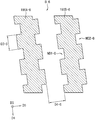
도 13 내지 도 18을 참조하면, 패드 영역의 상부에서 패드 배선들 각각은 패드 배선의 특성 및 배치에 따라 노치들이 다양한 방법으로 형성될 수 있다. 즉, 패드 배선은 유기막으로 덮이지 않을 수 있으므로, 제조 공정 중 또는 제조 공정 후에 직선으로 긴 파티클이 발생하지 않도록 패드 배선들 각각은 패드 영역의 적어도 일부에서 노치들을 포함할 수 있다.13 to 18, each of the pad wirings on the upper portion of the pad region may be formed in various ways according to the characteristics and arrangement of the pad wirings. That is, since the pad wirings may not be covered with the organic film, each of the pad wirings may include notches in at least a part of the pad area so as to prevent generation of long particles in a straight line during the manufacturing process or after the manufacturing process.
도 13에 도시된 바와 같이, 패드 배선들(190A-1, 190B-1) 각각은 패드 영역의 적어도 일부(B-1)에서 삼각형 모양을 갖는 노치(NO-1)들을 포함할 수 있다. 노치(NO-1)들은 패드 배선들(190A-1, 190B-1)이 패드 영역(NR)에서 연장되는 제4 방향(D4)에 대해 일정한 간격으로 형성되고, 인접한 두 개의 노치(NO-1)들 사이의 제3 거리(D3-1)는 인접한 두 개의 패드 배선들(190A-1, 190B-1) 사이의 제4 거리(D4-1)보다 작을 수 있다.As shown in FIG. 13, each of the
도 14에 도시된 바와 같이, 패드 배선들(190A-2, 190B-2) 각각은 패드 영역의 적어도 일부(B-2)에서 반원형 모양을 갖는 노치(NO-2)들을 포함할 수 있다. 노치(NO-2)들은 제4 방향(D4)에 대해 일정한 간격으로 형성되고, 인접한 두 개의 노치(NO-1)들 사이의 제3 거리(D3-2)는 인접한 두 개의 패드 배선들(190A-2, 190B-2) 사이의 제4 거리(D4-2)보다 작을 수 있다.As shown in FIG. 14, each of the
일반적으로, 노치(NO-2)에 의해 패드 배선들(190A-2, 190B-2)의 배선폭(line width)이 작아지는 경우, 패드 배선들(190A-2, 190B-2)의 저항이 증가될 수 있다. 또한, 배선폭이 균일한 경우보다 불균일한 경우 상대적으로 패드 배선들(190A-2, 190B-2)의 저항이 증가될 수 있다. 따라서, 노치(NO-2)에 의해 감소하는 배선폭의 정도를 낮추면서도 배선폭의 균일한 정도를 높일 수 있도록, 노치(NO-2)는 반원형 모양을 갖고 전기적 신호 전달의 효율성을 높일 수 있다.In general, when the line width of the
도 15 및 도 16에 도시된 바와 같이, 벤딩 영역(BR)에서와 마찬가지로 패드 배선들(190A-3, 190B-3) 각각은 패드 영역의 적어도 일부(B-3)에서 직사각형 모양을 갖는 노치(NO-3)들을 포함하거나, 패드 배선들(190A-4, 190B-4) 각각은 패드 영역의 적어도 일부(B-4)에서 사다리꼴 모양을 갖는 노치(NO-4)들을 포함할 수 있다. 인접한 두 개의 노치(NO-3 또는 NO-4)들 사이의 제3 거리(D3-3 또는 D3-4)는 인접한 두 개의 패드 배선들 사이의 제4 거리(D4-3 또는 D4-4)보다 작을 수 있다.As shown in Figs. 15 and 16, as in the bending region BR, each of the
도 17에 도시된 바와 같이, 패드 배선들(190A-5, 190B-5) 각각은 패드 영역의 적어도 일부(B-5)에서 삼각형 모양을 갖는 노치(NO-5)들을 포함할 수 있다. 인접한 두 개의 노치(NO-5)들 사이의 제3 거리(D3-5)는 인접한 두 개의 패드 배선들(190A-5, 190B-5) 사이의 제4 거리(D4-5)보다 작을 수 있다. 도 17에 도시된 패드 배선들(190A-5, 190B-5)은 도 13에 도시된 패드 배선들(190A-1, 190B-1)에 비해 상대적으로 짧은 간격으로 노치(NO-5)들이 형성되는 반면, 상대적으로 작의 크기의 노치(NO-5)를 포함할 수 있다. 이에 따라, 도 17에 도시된 패드 배선들(190A-5, 190B-5)은 도 13에 도시된 패드 배선들(190A-1, 190B-1)이 비해 배선폭을 전반적으로 크게 형성함에 따라 전기적 신호 전달의 효율성을 높일 수 있다.As shown in Fig. 17, each of the
비록, 도 13 내지 도 17의 실시예들에서는 패드 영역(NR) 상에서 패드 배선들의 제1 측면에 형성된 노치들과 제2 측면에 형성된 노치들은 패드 배선들이 연장된 제4 방향(D4)에 대해 서로 대칭적으로 배치되는 것으로 도시하였으나, 이에 한정되지 않는다. 예를 들어, 도 18에 도시된 바와 같이, 패드 배선들(190A-6, 190B-6)은 패드 영역의 적어도 일부(B-6)에서 제1 측면에 위치하는 제3 노치(NO1-6)들 및 제2 측면에 위치하는 제4 노치(NO2-6)들을 포함하고, 패드 배선들이 연장된 제4 방향(D4)과 직교하는 제5 방향(D5)에서 제3 노치(NO1-6)들은 제4 노치(NO2-6)들과 중첩되지 않을 수 있다. 이 경우에도 마찬가지로, 인접한 두 개의 제3 노치(NO1-6)들 사이 또는 인접한 두 개의 제4 노치(NO2-6)들 사이의 제3 거리(D3-6)는 인접한 두 개의 패드 배선들(190A-6, 190B-6) 사이의 제4 거리(D4-6)보다 작을 수 있다.In the embodiments of Figs. 13 to 17, the notches formed on the first side of the pad wirings and the notches formed on the second side on the pad region NR are formed in the fourth direction D4 in which the pad wirings extend But they are not limited thereto. For example, as shown in FIG. 18, the
비록, 도 13 내지 도 17의 실시예들에서는 패드 영역(NR) 상에서 패드 배선들의 노치들이 삼각형, 직사각형, 사다리꼴, 반원형 중 하나의 모양을 갖는 것으로 도시하였으나, 이에 한정되지 않는다. 예를 들어, 노치들은 그 외의 다각형 모양을 갖거나, 패드 배선들의 제1 측면에 형성된 노치들과 제2 측면에 형성된 노치들은 서로 다른 모양을 가질 수 있다.Although the embodiments of FIGS. 13 to 17 illustrate that the notches of the pad interconnections on the pad region NR have a shape of one of triangular, rectangular, trapezoid, or semicircular, but are not limited thereto. For example, the notches may have other polygonal shapes, or the notches formed on the first side of the pad lines and the notches formed on the second side may have different shapes.
비록, 도 6 내지 도 12의 실시예들에서는 패드 영역(NR) 상에서 배선들에 노치들이 일정한 간격으로 형성되는 것으로 도시하였으나, 이에 한정되지 않는다. 일 실시예에서, 노치들은 패드 영역(NR)에서 벤딩 영역(BR)과 멀어짐에 따라 인접한 두 개의 노치들 사이의 거리가 길어지도록 형성될 수 있다.Although the embodiments of FIGS. 6 to 12 illustrate that the notches are formed in the wirings on the pad region NR at regular intervals, the present invention is not limited thereto. In one embodiment, the notches may be formed such that the distance between the adjacent two notches increases as the pad region NR is away from the bending region BR.
도 19 및 도 20은 도 1의 표시 장치의 효과를 설명하기 위한 도면들이다.19 and 20 are views for explaining the effect of the display device of FIG.
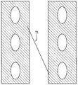
도 19 및 도 20을 참조하면, 벤딩 영역 및 패드 영역에서 연결 배선에 노치들을 형성하고, 인접한 노치들 사이의 간격(즉, 배선 직선부의 길이)가 인접한 배선들 사이의 거리보다 짧게 형성함으로써 제조 공정 중(특히, 연결 배선이 유기층으로 덮이기 이전의 공정) 벤딩 영역 및 패드 영역에서 발생되는 인접한 배선들 사이의 단락을 방지할 수 있다.19 and 20, notches are formed in the interconnecting interconnections in the bending region and the pad region, and the distance between the adjacent notches (i.e., the length of the straight line portions) is made shorter than the distance between adjacent interconnects, (In particular, the process before the connection wiring is covered with the organic layer) can be prevented from being short-circuited between adjacent wirings generated in the bending region and the pad region.
비교 실시예에 따른 연결 배선에서, 도 19에 도시된 바와 같이, 연결 배선이 측면에서 직선 모양을 갖는 경우, 표시 장치의 제조 공정에서 인접한 연결 배선들 사이의 거리보다 큰 제1 파티클(T1)이 생성될 수 있다. 제1 파티클(T1)에 의해 연결 배선들 간에 단락에 의해 불량이 발생할 수 있다. 특히, 해상도가 높은 표시 장치에서는 연결 배선들 사이의 간격이 상대적으로 작아질 수 있으며, 벤딩 영역을 포함하는 표시 장치에서 단락에 의한 불량이 빈번하게 발생할 수 있다.In the connection wiring according to the comparative example, as shown in Fig. 19, when the connection wiring has a linear shape on the side, the first particle T1, which is larger than the distance between the adjacent connection wirings in the manufacturing process of the display device, Lt; / RTI > Defects may be caused by shorting between the connection wirings by the first particle T1. Particularly, in a display device having a high resolution, a gap between connection wirings can be relatively small, and defects due to a short circuit frequently occur in a display device including a bending region.
반면에, 도 20에 도시된 바와 같이, 본 발명에 따른 연결 배선은 벤딩 영역에서 직선으로 길게 연장되지 않도록 노치를 형성할 수 있다. 이 경우, 표시 장치의 제조 공정에서 제2 파티클(T2)이 생성되더라도, 제2 파티클(T2)의 길이는 인접한 연결 배선들 사이의 거리보다 작을 수 있다. 이에 따라, 연결 배선들 간에 단락을 방지할 수 있으므로, 표시 장치의 제조 수율을 향상시킬 수 있고, 제조 비용이 절감될 수 있다. 이 경우, Quad HD의 해상도를 갖는 표시 장치를 제조할 때, 약 0.5%의 제조 수율이 향상되었다.On the other hand, as shown in FIG. 20, the connection wiring according to the present invention can form a notch so as not to extend in a straight line in the bending region. In this case, even if the second particle T2 is generated in the manufacturing process of the display device, the length of the second particle T2 may be smaller than the distance between the adjacent connection wirings. As a result, a short circuit between the connection wirings can be prevented, so that the manufacturing yield of the display device can be improved and the manufacturing cost can be reduced. In this case, when manufacturing a display device having a resolution of Quad HD, a manufacturing yield of about 0.5% was improved.
따라서, 본 발명의 실시예들에 따른 표시 장치는 배선들에 노치들을 형성함으로써, 제조 공정 중 유기막으로 덮이지 않고 노출된 배선들에서 발생되는 인접한 배선들 사이의 단락(short)을 방지할 수 있다. 비록, 상기에서는 연결 배선들 및/또는 패드 배선들이 벤딩 영역 또는 패드 영역에서 노치들을 형성되는 것으로 설명하였으나, 제조 공정 중 유기막으로 덮이지 않고 노출되는 다양한 위치의 배선들에 노치들이 형성될 수 있다.Thus, the display device according to the embodiments of the present invention can prevent not shorting between adjacent wirings generated in the exposed wirings without being covered with the organic film during the manufacturing process by forming the notches in the wirings have. Although the interconnecting interconnects and / or pad interconnections have been described above as forming notches in the bending region or pad region, notches can be formed in the interconnects at various locations exposed during the fabrication process without being covered by the organic film .
이상, 본 발명의 실시예들에 따른 표시 장치에 대하여 도면을 참조하여 설명하였지만, 상기 설명은 예시적인 것으로서 본 발명의 기술적 사상을 벗어나지 않는 범위에서 해당 기술 분야에서 통상의 지식을 가진 자에 의하여 수정 및 변경될 수 있을 것이다. 예를 들어, 상기에서는 표시 장치가 유기 발광 표시 장치인 것으로 설명하였으나, 표시 장치의 종류는 이에 한정되는 것이 아니다. 또한, 상기에서는 구동 회로가 COP 방식으로 기판에 실장되는 것으로 도시하였으나, 구동 회로가 연결되는 방식은 이에 한정되지 않는다.While the present invention has been particularly shown and described with reference to exemplary embodiments thereof, the above description is illustrative and not restrictive, and various changes and modifications may be made by those skilled in the art without departing from the technical spirit of the invention. And may be changed. For example, in the above description, the display device is an organic light emitting display device, but the display device is not limited thereto. In the above description, the driving circuit is mounted on the substrate by the COP method, but the manner in which the driving circuit is connected is not limited to this.
본 발명은 표시 장치를 구비한 전자 기기에 다양하게 적용될 수 있다. 예를 들어, 본 발명은 컴퓨터, 노트북, 휴대폰, 스마트폰, 스마트패드, 피엠피(PMP), 피디에이(PDA), MP3 플레이어, 디지털 카메라, 비디오 캠코더 등에 적용될 수 있다.The present invention can be variously applied to an electronic apparatus having a display device. For example, the present invention can be applied to a computer, a notebook, a mobile phone, a smart phone, a smart pad, a PMP, a PDA, an MP3 player, a digital camera, a video camcorder,
상기에서는 본 발명의 실시예들을 참조하여 설명하였지만, 해당 기술분야에서 통상의 지식을 가진 자는 하기의 특허청구범위에 기재된 본 발명의 사상 및 영역으로부터 벗어나지 않는 범위 내에서 본 발명을 다양하게 수정 및 변경시킬 수 있음을 이해할 것이다.While the present invention has been particularly shown and described with reference to exemplary embodiments thereof, it will be understood by those skilled in the art that various changes and modifications may be made therein without departing from the spirit and scope of the invention as defined in the appended claims. You will understand.
DR: 표시 영역
BR: 벤딩 영역
NR: 패드 영역
100: 표시 패널
110: 기판
120: 반도체 소자
140: 화소 구조물
170: 박막 봉지 구조물
180: 연결 배선
300: 구동 회로
1000: 표시 장치DR: Display area BR: Bending area
NR: Pad area 100: Display panel
110: substrate 120: semiconductor element
140: pixel structure 170: thin film encapsulation structure
180: connection wiring 300: driving circuit
1000: display device
Claims (23)
상기 기판의 상기 표시 영역 상에 배치되는 화소 구조물들;
상기 기판의 상기 패드 영역 상에 배치되는 패드 배선들; 및
상기 패드 배선들과 상기 화소 구조물들을 전기적으로 연결하고, 상기 벤딩 영역 상에서 복수의 노치(notch)들을 각각 포함하는 복수의 연결 배선들을 포함하는 표시 장치.A substrate including a display region, a pad region spaced apart from the display region, and a bending region located between the display region and the pad region;
Pixel structures disposed on the display region of the substrate;
Pad wirings disposed on the pad region of the substrate; And
And a plurality of connection wirings electrically connecting the pad wirings and the pixel structures, each of the plurality of connection wirings including a plurality of notches on the bending area.
상기 홀들은 상기 제1 방향과 직교하는 제2 방향에서 상기 노치들과 중첩되지 않는 것을 특징으로 하는 표시 장치.4. The semiconductor device of claim 3, wherein the interconnecting interconnections extend in a first direction on the bending region,
And the holes are not overlapped with the notches in a second direction orthogonal to the first direction.
상기 제1 노치들은 상기 제1 방향과 직교하는 제2 방향에서 상기 제2 노치들과 중첩되지 않는 것을 특징으로 하는 표시 장치.7. The semiconductor device of claim 6, wherein the interconnecting interconnections extend in a first direction on the bending region,
And the first notches do not overlap with the second notches in a second direction orthogonal to the first direction.
상기 제1 노치들은 상기 제1 방향에 대해 상기 제2 노치들에 대칭으로 배치되는 것을 특징으로 하는 표시 장치.7. The semiconductor device of claim 6, wherein the interconnecting interconnections extend in a first direction on the bending region,
Wherein the first notches are symmetrically disposed with respect to the second notches in the first direction.
상기 제3 노치들은 상기 제3 방향과 직교하는 제4 방향에서 상기 제4 노치들과 중첩되지 않는 것을 특징으로 하는 표시 장치.11. The semiconductor device according to claim 10, wherein the pad wirings extend in a third direction,
And the third notches do not overlap with the fourth notches in a fourth direction orthogonal to the third direction.
상기 제3 노치들은 상기 제3 방향에 대해 상기 제4 노치들에 대칭으로 배치되는 것을 특징으로 하는 표시 장치.11. The semiconductor device according to claim 10, wherein the pad wirings extend in a third direction,
And the third notches are arranged symmetrically to the fourth notches with respect to the third direction.
제1 금속층;
알루미늄(Al)을 포함하고, 상기 제1 금속층 상에 배치되는 제2 금속층; 및
상기 제2 금속층 상에 배치되는 제3 금속층을 포함하는 것을 특징으로 하는 표시 장치.2. The semiconductor device according to claim 1,
A first metal layer;
A second metal layer comprising aluminum (Al) and disposed on the first metal layer; And
And a third metal layer disposed on the second metal layer.
상기 표시 영역 및 상기 패드 영역에 상응하는 상기 표시 패널의 저면 상에 배치되는 하부 보호 필름; 및
상기 기판 및 상기 하부 보호 필름 사이에 배치되는 접착층을 더 포함하는 것을 특징으로 하는 표시 장치.The method according to claim 1,
A lower protective film disposed on a bottom surface of the display panel corresponding to the display area and the pad area; And
And an adhesive layer disposed between the substrate and the lower protective film.
상기 기판의 상기 표시 영역 상에 배치되는 화소 구조물들;
상기 화소 구조물들에 구동 신호를 제공하는 구동 회로; 및
상기 구동 회로와 상기 화소 구조물들을 전기적으로 연결하고, 상기 벤딩 영역 상에서 복수의 노치들을 각각 포함하는 복수의 연결 배선들을 포함하는 표시 장치.A substrate including a display region, a pad region spaced apart from the display region, and a bending region located between the display region and the pad region;
Pixel structures disposed on the display region of the substrate;
A driving circuit for providing driving signals to the pixel structures; And
And a plurality of connection wirings electrically connecting the driving circuit and the pixel structures and including a plurality of notches on the bending area.
상기 연결 배선들은 상기 기판의 상기 패드 영역 상에 배치되는 패드 배선들 및 상기 패드 배선들과 연결되는 도전 패턴들을 통해 상기 구동 회로와 연결되는 것을 특징으로 하는 표시 장치.18. The semiconductor memory device according to claim 17, wherein the driving circuit is located on the pad region,
Wherein the connection wirings are connected to the driving circuit through pad wirings disposed on the pad region of the substrate and conductive patterns connected to the pad wirings.
23. The display device of claim 22, wherein each of the pad wirings includes third notches formed on a first side face on the pad region and fourth notches formed on a second side opposite to the first side face. .
Priority Applications (7)
| Application Number | Priority Date | Filing Date | Title |
|---|---|---|---|
| KR1020170024982A KR102783141B1 (en) | 2017-02-24 | 2017-02-24 | Display device |
| US15/661,122 US10269890B2 (en) | 2017-02-24 | 2017-07-27 | Display device having notched connection wiring |
| EP20160773.6A EP3686934B1 (en) | 2017-02-24 | 2017-10-24 | Display device having notched connection wiring |
| EP17198097.2A EP3367440B1 (en) | 2017-02-24 | 2017-10-24 | Display device having notched connection wiring |
| CN201711054499.4A CN108511483B (en) | 2017-02-24 | 2017-11-01 | Display device with recessed connection wiring |
| US16/358,322 US10748980B2 (en) | 2017-02-24 | 2019-03-19 | Display device having notched connection wiring |
| US16/928,807 US11342405B2 (en) | 2017-02-24 | 2020-07-14 | Display device having notched connection wiring |
Applications Claiming Priority (1)
| Application Number | Priority Date | Filing Date | Title |
|---|---|---|---|
| KR1020170024982A KR102783141B1 (en) | 2017-02-24 | 2017-02-24 | Display device |
Publications (2)
| Publication Number | Publication Date |
|---|---|
| KR20180098451A true KR20180098451A (en) | 2018-09-04 |
| KR102783141B1 KR102783141B1 (en) | 2025-03-20 |
Family
ID=60186053
Family Applications (1)
| Application Number | Title | Priority Date | Filing Date |
|---|---|---|---|
| KR1020170024982A Active KR102783141B1 (en) | 2017-02-24 | 2017-02-24 | Display device |
Country Status (4)
| Country | Link |
|---|---|
| US (3) | US10269890B2 (en) |
| EP (2) | EP3686934B1 (en) |
| KR (1) | KR102783141B1 (en) |
| CN (1) | CN108511483B (en) |
Families Citing this family (19)
| Publication number | Priority date | Publication date | Assignee | Title |
|---|---|---|---|---|
| KR102783141B1 (en) | 2017-02-24 | 2025-03-20 | 삼성디스플레이 주식회사 | Display device |
| JP2018205337A (en) * | 2017-05-30 | 2018-12-27 | 株式会社ジャパンディスプレイ | Display device |
| KR102337750B1 (en) * | 2017-11-06 | 2021-12-10 | 삼성디스플레이 주식회사 | Display device and method of manufacturing the same |
| CN108565268B (en) * | 2018-04-02 | 2021-02-12 | 昆山国显光电有限公司 | Array substrate and display screen |
| CN109494314B (en) * | 2018-10-16 | 2020-12-08 | 武汉华星光电半导体显示技术有限公司 | A flexible OLED display panel and preparation method thereof |
| CN109585700B (en) * | 2018-12-14 | 2020-06-19 | 京东方科技集团股份有限公司 | A display substrate, its manufacturing method, and a display device |
| CN109599403B (en) * | 2018-12-19 | 2021-02-26 | 武汉华星光电半导体显示技术有限公司 | Metal routing |
| CN109638060B (en) * | 2018-12-21 | 2020-10-27 | 武汉华星光电半导体显示技术有限公司 | Array substrate and flexible display panel |
| CN109655957B (en) * | 2019-01-08 | 2021-06-22 | 昆山工研院新型平板显示技术中心有限公司 | Polaroid and manufacturing method thereof, display panel and display device |
| KR102688018B1 (en) * | 2019-05-13 | 2024-07-25 | 삼성디스플레이 주식회사 | Nput sensing unit, display device including same, and method for manufacturing same |
| CN110335544B (en) * | 2019-06-18 | 2020-12-25 | 武汉华星光电半导体显示技术有限公司 | OLED display panel and display device |
| KR102752716B1 (en) * | 2019-10-28 | 2025-01-08 | 엘지디스플레이 주식회사 | Flexible display device |
| CN110767731B (en) * | 2019-10-31 | 2022-05-20 | 京东方科技集团股份有限公司 | Display panel and display device |
| CN111009565B (en) * | 2019-12-11 | 2022-06-17 | 昆山国显光电有限公司 | Display substrate, manufacturing method of display substrate and display panel |
| KR102923874B1 (en) | 2020-02-11 | 2026-02-09 | 삼성디스플레이 주식회사 | Display device |
| EP4165448B1 (en) * | 2020-06-11 | 2025-09-03 | Signify Holding B.V. | Lens plate |
| CN111580313B (en) * | 2020-06-16 | 2022-09-02 | 京东方科技集团股份有限公司 | Array substrate, display module, electronic equipment and manufacturing method of array substrate |
| WO2023162094A1 (en) * | 2022-02-24 | 2023-08-31 | シャープディスプレイテクノロジー株式会社 | Display device |
| CN114628062B (en) * | 2022-03-28 | 2023-06-02 | Tcl华星光电技术有限公司 | Conductive film and display panel |
Citations (1)
| Publication number | Priority date | Publication date | Assignee | Title |
|---|---|---|---|---|
| US20160035812A1 (en) * | 2014-07-31 | 2016-02-04 | Lg Display Co., Ltd. | Flexible display device with wire having reinforced portion and manufacturing method for the same |
Family Cites Families (16)
| Publication number | Priority date | Publication date | Assignee | Title |
|---|---|---|---|---|
| JPH06216475A (en) * | 1993-01-21 | 1994-08-05 | Matsushita Electric Ind Co Ltd | Flexible board |
| EP1388171A1 (en) * | 2001-05-03 | 2004-02-11 | Koninklijke Philips Electronics N.V. | Electroluminescent device |
| WO2010086033A1 (en) * | 2009-01-30 | 2010-08-05 | Interuniversitair Microelektronica Centrum Vzw | Stretchable electronic device |
| WO2011148664A1 (en) | 2010-05-24 | 2011-12-01 | シャープ株式会社 | Active matrix substrate and liquid crystal display device |
| TWI419094B (en) * | 2010-09-10 | 2013-12-11 | Au Optronics Corp | Flexible display panel |
| KR101931338B1 (en) | 2011-10-19 | 2018-12-21 | 엘지디스플레이 주식회사 | Flexible Printed Circuit Board and Display Device using the same |
| US9203050B2 (en) | 2013-05-21 | 2015-12-01 | Samsung Display Co., Ltd. | Organic light emitting diode display and method of manufacturing the same |
| US9788789B2 (en) * | 2013-08-30 | 2017-10-17 | Thalmic Labs Inc. | Systems, articles, and methods for stretchable printed circuit boards |
| KR102085961B1 (en) | 2013-12-24 | 2020-03-06 | 엘지디스플레이 주식회사 | Flexible organic light emitting display and method of manufacturing the same |
| JP6285275B2 (en) | 2014-04-30 | 2018-02-28 | 株式会社Screenホールディングス | Substrate processing apparatus and substrate processing method |
| US20160003581A1 (en) * | 2014-07-03 | 2016-01-07 | David Warren | Plate carrier and a protective vest |
| US9349758B2 (en) | 2014-09-30 | 2016-05-24 | Lg Display Co., Ltd. | Flexible display device with divided power lines and manufacturing method for the same |
| US20160105950A1 (en) * | 2014-10-10 | 2016-04-14 | Apple Inc. | Electronic Device Having Structured Flexible Substrates With Bends |
| KR20160125593A (en) | 2015-04-21 | 2016-11-01 | 삼성디스플레이 주식회사 | Flexible display apparatus |
| KR102583831B1 (en) * | 2016-11-25 | 2023-09-27 | 엘지디스플레이 주식회사 | Flexible Electroluminescent Display Device |
| KR102783141B1 (en) | 2017-02-24 | 2025-03-20 | 삼성디스플레이 주식회사 | Display device |
-
2017
- 2017-02-24 KR KR1020170024982A patent/KR102783141B1/en active Active
- 2017-07-27 US US15/661,122 patent/US10269890B2/en active Active
- 2017-10-24 EP EP20160773.6A patent/EP3686934B1/en active Active
- 2017-10-24 EP EP17198097.2A patent/EP3367440B1/en active Active
- 2017-11-01 CN CN201711054499.4A patent/CN108511483B/en active Active
-
2019
- 2019-03-19 US US16/358,322 patent/US10748980B2/en active Active
-
2020
- 2020-07-14 US US16/928,807 patent/US11342405B2/en active Active
Patent Citations (1)
| Publication number | Priority date | Publication date | Assignee | Title |
|---|---|---|---|---|
| US20160035812A1 (en) * | 2014-07-31 | 2016-02-04 | Lg Display Co., Ltd. | Flexible display device with wire having reinforced portion and manufacturing method for the same |
Also Published As
| Publication number | Publication date |
|---|---|
| US11342405B2 (en) | 2022-05-24 |
| KR102783141B1 (en) | 2025-03-20 |
| EP3367440A1 (en) | 2018-08-29 |
| EP3686934B1 (en) | 2025-06-04 |
| US10269890B2 (en) | 2019-04-23 |
| US10748980B2 (en) | 2020-08-18 |
| EP3686934A1 (en) | 2020-07-29 |
| US20180247992A1 (en) | 2018-08-30 |
| EP3367440B1 (en) | 2020-04-22 |
| US20190214453A1 (en) | 2019-07-11 |
| US20200343333A1 (en) | 2020-10-29 |
| CN108511483A (en) | 2018-09-07 |
| CN108511483B (en) | 2023-09-19 |
Similar Documents
| Publication | Publication Date | Title |
|---|---|---|
| KR102783141B1 (en) | Display device | |
| CN111129270B (en) | Micro LED display device | |
| CN112951867B (en) | Display device | |
| CN108962947B (en) | Flexible display panel and display device | |
| US9978823B2 (en) | Organic light emitting display device and method for manufacturing the same | |
| KR102903911B1 (en) | Display device and method for fabrication thereof | |
| CN108153442A (en) | Touch display device | |
| JP2019046175A (en) | Display device | |
| CN104347673A (en) | Organic light emitting display device and manufacturing method thereof | |
| KR20170012664A (en) | Thin Film Transistor Array Substrate And Organic Light Emitting Diode Display Device Including The Same | |
| CN103633112A (en) | Organic light emitting diode display device | |
| CN114503274A (en) | Display substrate and display device | |
| CN113517262A (en) | Display panel, method for making the same, and display device | |
| CN114664911A (en) | Display substrate and display device | |
| JP2015015114A (en) | Organic electroluminescent display device | |
| CN120548068A (en) | Display panel, display device and equipment | |
| CN114356154B (en) | Touch control substrate and display device | |
| KR102466918B1 (en) | Chip on film package and display device including the chip on film package | |
| KR20230102354A (en) | Display device | |
| CN116471879A (en) | Display device and method of manufacturing same | |
| CN115458534A (en) | Display module and display device | |
| KR20180079481A (en) | Organic light emitting display device | |
| KR20220130286A (en) | Display device and manufacturing method thereof | |
| US20230145007A1 (en) | Display device | |
| US12426412B2 (en) | Display device |
Legal Events
| Date | Code | Title | Description |
|---|---|---|---|
| PA0109 | Patent application |
St.27 status event code: A-0-1-A10-A12-nap-PA0109 |
|
| PG1501 | Laying open of application |
St.27 status event code: A-1-1-Q10-Q12-nap-PG1501 |
|
| R18-X000 | Changes to party contact information recorded |
St.27 status event code: A-3-3-R10-R18-oth-X000 |
|
| P22-X000 | Classification modified |
St.27 status event code: A-2-2-P10-P22-nap-X000 |
|
| P22-X000 | Classification modified |
St.27 status event code: A-2-2-P10-P22-nap-X000 |
|
| A201 | Request for examination | ||
| PA0201 | Request for examination |
St.27 status event code: A-1-2-D10-D11-exm-PA0201 |
|
| P22-X000 | Classification modified |
St.27 status event code: A-2-2-P10-P22-nap-X000 |
|
| P22-X000 | Classification modified |
St.27 status event code: A-2-2-P10-P22-nap-X000 |
|
| E902 | Notification of reason for refusal | ||
| PE0902 | Notice of grounds for rejection |
St.27 status event code: A-1-2-D10-D21-exm-PE0902 |
|
| E13-X000 | Pre-grant limitation requested |
St.27 status event code: A-2-3-E10-E13-lim-X000 |
|
| P11-X000 | Amendment of application requested |
St.27 status event code: A-2-2-P10-P11-nap-X000 |
|
| P13-X000 | Application amended |
St.27 status event code: A-2-2-P10-P13-nap-X000 |
|
| P22-X000 | Classification modified |
St.27 status event code: A-2-2-P10-P22-nap-X000 |
|
| E701 | Decision to grant or registration of patent right | ||
| PE0701 | Decision of registration |
St.27 status event code: A-1-2-D10-D22-exm-PE0701 |
|
| PR0701 | Registration of establishment |
St.27 status event code: A-2-4-F10-F11-exm-PR0701 |
|
| PR1002 | Payment of registration fee |
St.27 status event code: A-2-2-U10-U11-oth-PR1002 |
|
| PG1601 | Publication of registration |
St.27 status event code: A-4-4-Q10-Q13-nap-PG1601 |