KR20180098356A - 이방성 도전 필름 - Google Patents
이방성 도전 필름 Download PDFInfo
- Publication number
- KR20180098356A KR20180098356A KR1020187021397A KR20187021397A KR20180098356A KR 20180098356 A KR20180098356 A KR 20180098356A KR 1020187021397 A KR1020187021397 A KR 1020187021397A KR 20187021397 A KR20187021397 A KR 20187021397A KR 20180098356 A KR20180098356 A KR 20180098356A
- Authority
- KR
- South Korea
- Prior art keywords
- anisotropic conductive
- conductive film
- conductive particles
- film
- insulating resin
- Prior art date
- Legal status (The legal status is an assumption and is not a legal conclusion. Google has not performed a legal analysis and makes no representation as to the accuracy of the status listed.)
- Granted
Links
Images


Classifications
-
- C—CHEMISTRY; METALLURGY
- C09—DYES; PAINTS; POLISHES; NATURAL RESINS; ADHESIVES; COMPOSITIONS NOT OTHERWISE PROVIDED FOR; APPLICATIONS OF MATERIALS NOT OTHERWISE PROVIDED FOR
- C09J—ADHESIVES; NON-MECHANICAL ASPECTS OF ADHESIVE PROCESSES IN GENERAL; ADHESIVE PROCESSES NOT PROVIDED FOR ELSEWHERE; USE OF MATERIALS AS ADHESIVES
- C09J9/00—Adhesives characterised by their physical nature or the effects produced, e.g. glue sticks
- C09J9/02—Electrically-conducting adhesives
-
- H—ELECTRICITY
- H01—ELECTRIC ELEMENTS
- H01B—CABLES; CONDUCTORS; INSULATORS; SELECTION OF MATERIALS FOR THEIR CONDUCTIVE, INSULATING OR DIELECTRIC PROPERTIES
- H01B1/00—Conductors or conductive bodies characterised by the conductive materials; Selection of materials as conductors
- H01B1/20—Conductive material dispersed in non-conductive organic material
- H01B1/22—Conductive material dispersed in non-conductive organic material the conductive material comprising metals or alloys
-
- H—ELECTRICITY
- H01—ELECTRIC ELEMENTS
- H01B—CABLES; CONDUCTORS; INSULATORS; SELECTION OF MATERIALS FOR THEIR CONDUCTIVE, INSULATING OR DIELECTRIC PROPERTIES
- H01B13/00—Apparatus or processes specially adapted for manufacturing conductors or cables
-
- H—ELECTRICITY
- H01—ELECTRIC ELEMENTS
- H01B—CABLES; CONDUCTORS; INSULATORS; SELECTION OF MATERIALS FOR THEIR CONDUCTIVE, INSULATING OR DIELECTRIC PROPERTIES
- H01B13/00—Apparatus or processes specially adapted for manufacturing conductors or cables
- H01B13/0016—Apparatus or processes specially adapted for manufacturing conductors or cables for heat treatment
-
- H—ELECTRICITY
- H01—ELECTRIC ELEMENTS
- H01B—CABLES; CONDUCTORS; INSULATORS; SELECTION OF MATERIALS FOR THEIR CONDUCTIVE, INSULATING OR DIELECTRIC PROPERTIES
- H01B13/00—Apparatus or processes specially adapted for manufacturing conductors or cables
- H01B13/0036—Details
-
- H—ELECTRICITY
- H01—ELECTRIC ELEMENTS
- H01B—CABLES; CONDUCTORS; INSULATORS; SELECTION OF MATERIALS FOR THEIR CONDUCTIVE, INSULATING OR DIELECTRIC PROPERTIES
- H01B5/00—Non-insulated conductors or conductive bodies characterised by their form
- H01B5/16—Non-insulated conductors or conductive bodies characterised by their form comprising conductive material in insulating or poorly conductive material, e.g. conductive rubber
-
- H—ELECTRICITY
- H01—ELECTRIC ELEMENTS
- H01R—ELECTRICALLY-CONDUCTIVE CONNECTIONS; STRUCTURAL ASSOCIATIONS OF A PLURALITY OF MUTUALLY-INSULATED ELECTRICAL CONNECTING ELEMENTS; COUPLING DEVICES; CURRENT COLLECTORS
- H01R11/00—Individual connecting elements providing two or more spaced connecting locations for conductive members which are, or may be, thereby interconnected, e.g. end pieces for wires or cables supported by the wire or cable and having means for facilitating electrical connection to some other wire, terminal, or conductive member, blocks of binding posts
- H01R11/01—Individual connecting elements providing two or more spaced connecting locations for conductive members which are, or may be, thereby interconnected, e.g. end pieces for wires or cables supported by the wire or cable and having means for facilitating electrical connection to some other wire, terminal, or conductive member, blocks of binding posts characterised by the form or arrangement of the conductive interconnection between the connecting locations
-
- H—ELECTRICITY
- H01—ELECTRIC ELEMENTS
- H01R—ELECTRICALLY-CONDUCTIVE CONNECTIONS; STRUCTURAL ASSOCIATIONS OF A PLURALITY OF MUTUALLY-INSULATED ELECTRICAL CONNECTING ELEMENTS; COUPLING DEVICES; CURRENT COLLECTORS
- H01R43/00—Apparatus or processes specially adapted for manufacturing, assembling, maintaining, or repairing of line connectors or current collectors or for joining electric conductors
-
- H—ELECTRICITY
- H10—SEMICONDUCTOR DEVICES; ELECTRIC SOLID-STATE DEVICES NOT OTHERWISE PROVIDED FOR
- H10W—GENERIC PACKAGES, INTERCONNECTIONS, CONNECTORS OR OTHER CONSTRUCTIONAL DETAILS OF DEVICES COVERED BY CLASS H10
- H10W74/00—Encapsulations, e.g. protective coatings
- H10W74/40—Encapsulations, e.g. protective coatings characterised by their materials
- H10W74/47—Encapsulations, e.g. protective coatings characterised by their materials comprising organic materials, e.g. plastics or resins
-
- H—ELECTRICITY
- H10—SEMICONDUCTOR DEVICES; ELECTRIC SOLID-STATE DEVICES NOT OTHERWISE PROVIDED FOR
- H10W—GENERIC PACKAGES, INTERCONNECTIONS, CONNECTORS OR OTHER CONSTRUCTIONAL DETAILS OF DEVICES COVERED BY CLASS H10
- H10W72/00—Interconnections or connectors in packages
- H10W72/01—Manufacture or treatment
- H10W72/013—Manufacture or treatment of die-attach connectors
- H10W72/01304—Manufacture or treatment of die-attach connectors using temporary auxiliary members, e.g. using sacrificial coatings or handle substrates
-
- H—ELECTRICITY
- H10—SEMICONDUCTOR DEVICES; ELECTRIC SOLID-STATE DEVICES NOT OTHERWISE PROVIDED FOR
- H10W—GENERIC PACKAGES, INTERCONNECTIONS, CONNECTORS OR OTHER CONSTRUCTIONAL DETAILS OF DEVICES COVERED BY CLASS H10
- H10W72/00—Interconnections or connectors in packages
- H10W72/01—Manufacture or treatment
- H10W72/013—Manufacture or treatment of die-attach connectors
- H10W72/01315—Forming coatings
-
- H—ELECTRICITY
- H10—SEMICONDUCTOR DEVICES; ELECTRIC SOLID-STATE DEVICES NOT OTHERWISE PROVIDED FOR
- H10W—GENERIC PACKAGES, INTERCONNECTIONS, CONNECTORS OR OTHER CONSTRUCTIONAL DETAILS OF DEVICES COVERED BY CLASS H10
- H10W72/00—Interconnections or connectors in packages
- H10W72/01—Manufacture or treatment
- H10W72/013—Manufacture or treatment of die-attach connectors
- H10W72/01321—Manufacture or treatment of die-attach connectors using local deposition
- H10W72/01325—Manufacture or treatment of die-attach connectors using local deposition in solid form
-
- H—ELECTRICITY
- H10—SEMICONDUCTOR DEVICES; ELECTRIC SOLID-STATE DEVICES NOT OTHERWISE PROVIDED FOR
- H10W—GENERIC PACKAGES, INTERCONNECTIONS, CONNECTORS OR OTHER CONSTRUCTIONAL DETAILS OF DEVICES COVERED BY CLASS H10
- H10W72/00—Interconnections or connectors in packages
- H10W72/01—Manufacture or treatment
- H10W72/013—Manufacture or treatment of die-attach connectors
- H10W72/01331—Manufacture or treatment of die-attach connectors using blanket deposition
- H10W72/01333—Manufacture or treatment of die-attach connectors using blanket deposition in liquid form, e.g. spin coating, spray coating or immersion coating
-
- H—ELECTRICITY
- H10—SEMICONDUCTOR DEVICES; ELECTRIC SOLID-STATE DEVICES NOT OTHERWISE PROVIDED FOR
- H10W—GENERIC PACKAGES, INTERCONNECTIONS, CONNECTORS OR OTHER CONSTRUCTIONAL DETAILS OF DEVICES COVERED BY CLASS H10
- H10W72/00—Interconnections or connectors in packages
- H10W72/01—Manufacture or treatment
- H10W72/013—Manufacture or treatment of die-attach connectors
- H10W72/01351—Changing the shapes of die-attach connectors
-
- H—ELECTRICITY
- H10—SEMICONDUCTOR DEVICES; ELECTRIC SOLID-STATE DEVICES NOT OTHERWISE PROVIDED FOR
- H10W—GENERIC PACKAGES, INTERCONNECTIONS, CONNECTORS OR OTHER CONSTRUCTIONAL DETAILS OF DEVICES COVERED BY CLASS H10
- H10W72/00—Interconnections or connectors in packages
- H10W72/071—Connecting or disconnecting
- H10W72/073—Connecting or disconnecting of die-attach connectors
- H10W72/07331—Connecting techniques
- H10W72/07332—Compression bonding, e.g. thermocompression bonding
-
- H—ELECTRICITY
- H10—SEMICONDUCTOR DEVICES; ELECTRIC SOLID-STATE DEVICES NOT OTHERWISE PROVIDED FOR
- H10W—GENERIC PACKAGES, INTERCONNECTIONS, CONNECTORS OR OTHER CONSTRUCTIONAL DETAILS OF DEVICES COVERED BY CLASS H10
- H10W72/00—Interconnections or connectors in packages
- H10W72/071—Connecting or disconnecting
- H10W72/074—Connecting or disconnecting of anisotropic conductive adhesives
-
- H—ELECTRICITY
- H10—SEMICONDUCTOR DEVICES; ELECTRIC SOLID-STATE DEVICES NOT OTHERWISE PROVIDED FOR
- H10W—GENERIC PACKAGES, INTERCONNECTIONS, CONNECTORS OR OTHER CONSTRUCTIONAL DETAILS OF DEVICES COVERED BY CLASS H10
- H10W72/00—Interconnections or connectors in packages
- H10W72/20—Bump connectors, e.g. solder bumps or copper pillars; Dummy bumps; Thermal bumps
- H10W72/231—Shapes
- H10W72/232—Plan-view shape, i.e. in top view
-
- H—ELECTRICITY
- H10—SEMICONDUCTOR DEVICES; ELECTRIC SOLID-STATE DEVICES NOT OTHERWISE PROVIDED FOR
- H10W—GENERIC PACKAGES, INTERCONNECTIONS, CONNECTORS OR OTHER CONSTRUCTIONAL DETAILS OF DEVICES COVERED BY CLASS H10
- H10W72/00—Interconnections or connectors in packages
- H10W72/20—Bump connectors, e.g. solder bumps or copper pillars; Dummy bumps; Thermal bumps
- H10W72/241—Dispositions, e.g. layouts
- H10W72/247—Dispositions of multiple bumps
- H10W72/248—Top-view layouts, e.g. mirror arrays
-
- H—ELECTRICITY
- H10—SEMICONDUCTOR DEVICES; ELECTRIC SOLID-STATE DEVICES NOT OTHERWISE PROVIDED FOR
- H10W—GENERIC PACKAGES, INTERCONNECTIONS, CONNECTORS OR OTHER CONSTRUCTIONAL DETAILS OF DEVICES COVERED BY CLASS H10
- H10W72/00—Interconnections or connectors in packages
- H10W72/20—Bump connectors, e.g. solder bumps or copper pillars; Dummy bumps; Thermal bumps
- H10W72/251—Materials
- H10W72/252—Materials comprising solid metals or solid metalloids, e.g. PbSn, Ag or Cu
-
- H—ELECTRICITY
- H10—SEMICONDUCTOR DEVICES; ELECTRIC SOLID-STATE DEVICES NOT OTHERWISE PROVIDED FOR
- H10W—GENERIC PACKAGES, INTERCONNECTIONS, CONNECTORS OR OTHER CONSTRUCTIONAL DETAILS OF DEVICES COVERED BY CLASS H10
- H10W72/00—Interconnections or connectors in packages
- H10W72/30—Die-attach connectors
- H10W72/321—Structures or relative sizes of die-attach connectors
- H10W72/322—Multilayered die-attach connectors, e.g. a coating on a top surface of a core
-
- H—ELECTRICITY
- H10—SEMICONDUCTOR DEVICES; ELECTRIC SOLID-STATE DEVICES NOT OTHERWISE PROVIDED FOR
- H10W—GENERIC PACKAGES, INTERCONNECTIONS, CONNECTORS OR OTHER CONSTRUCTIONAL DETAILS OF DEVICES COVERED BY CLASS H10
- H10W72/00—Interconnections or connectors in packages
- H10W72/30—Die-attach connectors
- H10W72/321—Structures or relative sizes of die-attach connectors
- H10W72/324—Die-attach connectors having multiple side-by-side cores
-
- H—ELECTRICITY
- H10—SEMICONDUCTOR DEVICES; ELECTRIC SOLID-STATE DEVICES NOT OTHERWISE PROVIDED FOR
- H10W—GENERIC PACKAGES, INTERCONNECTIONS, CONNECTORS OR OTHER CONSTRUCTIONAL DETAILS OF DEVICES COVERED BY CLASS H10
- H10W72/00—Interconnections or connectors in packages
- H10W72/30—Die-attach connectors
- H10W72/321—Structures or relative sizes of die-attach connectors
- H10W72/325—Die-attach connectors having a filler embedded in a matrix
-
- H—ELECTRICITY
- H10—SEMICONDUCTOR DEVICES; ELECTRIC SOLID-STATE DEVICES NOT OTHERWISE PROVIDED FOR
- H10W—GENERIC PACKAGES, INTERCONNECTIONS, CONNECTORS OR OTHER CONSTRUCTIONAL DETAILS OF DEVICES COVERED BY CLASS H10
- H10W72/00—Interconnections or connectors in packages
- H10W72/30—Die-attach connectors
- H10W72/351—Materials of die-attach connectors
- H10W72/352—Materials of die-attach connectors comprising metals or metalloids, e.g. solders
-
- H—ELECTRICITY
- H10—SEMICONDUCTOR DEVICES; ELECTRIC SOLID-STATE DEVICES NOT OTHERWISE PROVIDED FOR
- H10W—GENERIC PACKAGES, INTERCONNECTIONS, CONNECTORS OR OTHER CONSTRUCTIONAL DETAILS OF DEVICES COVERED BY CLASS H10
- H10W72/00—Interconnections or connectors in packages
- H10W72/30—Die-attach connectors
- H10W72/351—Materials of die-attach connectors
- H10W72/353—Materials of die-attach connectors not comprising solid metals or solid metalloids, e.g. ceramics
- H10W72/354—Materials of die-attach connectors not comprising solid metals or solid metalloids, e.g. ceramics comprising polymers
-
- H—ELECTRICITY
- H10—SEMICONDUCTOR DEVICES; ELECTRIC SOLID-STATE DEVICES NOT OTHERWISE PROVIDED FOR
- H10W—GENERIC PACKAGES, INTERCONNECTIONS, CONNECTORS OR OTHER CONSTRUCTIONAL DETAILS OF DEVICES COVERED BY CLASS H10
- H10W74/00—Encapsulations, e.g. protective coatings
- H10W74/10—Encapsulations, e.g. protective coatings characterised by their shape or disposition
- H10W74/15—Encapsulations, e.g. protective coatings characterised by their shape or disposition on active surfaces of flip-chip devices, e.g. underfills
-
- H—ELECTRICITY
- H10—SEMICONDUCTOR DEVICES; ELECTRIC SOLID-STATE DEVICES NOT OTHERWISE PROVIDED FOR
- H10W—GENERIC PACKAGES, INTERCONNECTIONS, CONNECTORS OR OTHER CONSTRUCTIONAL DETAILS OF DEVICES COVERED BY CLASS H10
- H10W90/00—Package configurations
- H10W90/701—Package configurations characterised by the relative positions of pads or connectors relative to package parts
- H10W90/721—Package configurations characterised by the relative positions of pads or connectors relative to package parts of bump connectors
- H10W90/724—Package configurations characterised by the relative positions of pads or connectors relative to package parts of bump connectors between a chip and a stacked insulating package substrate, interposer or RDL
-
- H—ELECTRICITY
- H10—SEMICONDUCTOR DEVICES; ELECTRIC SOLID-STATE DEVICES NOT OTHERWISE PROVIDED FOR
- H10W—GENERIC PACKAGES, INTERCONNECTIONS, CONNECTORS OR OTHER CONSTRUCTIONAL DETAILS OF DEVICES COVERED BY CLASS H10
- H10W90/00—Package configurations
- H10W90/701—Package configurations characterised by the relative positions of pads or connectors relative to package parts
- H10W90/731—Package configurations characterised by the relative positions of pads or connectors relative to package parts of die-attach connectors
- H10W90/734—Package configurations characterised by the relative positions of pads or connectors relative to package parts of die-attach connectors between a chip and a stacked insulating package substrate, interposer or RDL
-
- H—ELECTRICITY
- H10—SEMICONDUCTOR DEVICES; ELECTRIC SOLID-STATE DEVICES NOT OTHERWISE PROVIDED FOR
- H10W—GENERIC PACKAGES, INTERCONNECTIONS, CONNECTORS OR OTHER CONSTRUCTIONAL DETAILS OF DEVICES COVERED BY CLASS H10
- H10W99/00—Subject matter not provided for in other groups of this subclass
Landscapes
- Engineering & Computer Science (AREA)
- Manufacturing & Machinery (AREA)
- Chemical & Material Sciences (AREA)
- Physics & Mathematics (AREA)
- Dispersion Chemistry (AREA)
- Spectroscopy & Molecular Physics (AREA)
- Organic Chemistry (AREA)
- Thermal Sciences (AREA)
- Non-Insulated Conductors (AREA)
- Manufacturing Of Electrical Connectors (AREA)
Abstract
Description
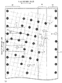
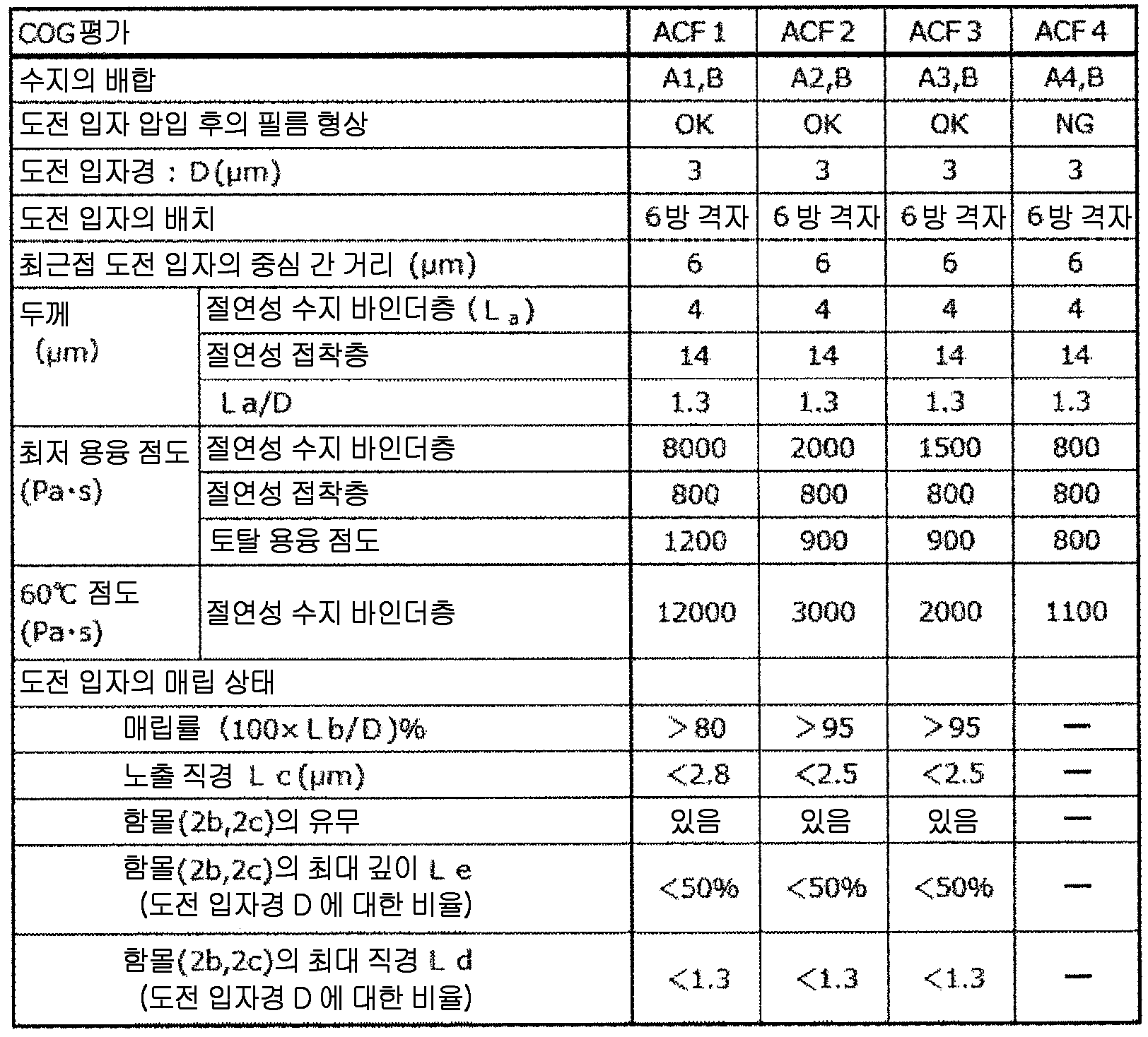
도 2 는, 실시예의 이방성 도전 필름 (1B) 의 도전 입자의 배치를 설명하는 평면도이다.
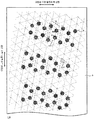
도 3 은, 실시예의 이방성 도전 필름 (1C) 의 도전 입자의 배치를 설명하는 평면도이다.
도 4 는, COG 용의 이방성 도전 필름에 있어서 도전 입자의 배치가 규격 외인 지점의 위치를 나타내는 평면도이다.
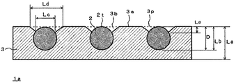
도 5 는, 실시예의 이방성 도전 필름 (1a) 의 단면도이다.
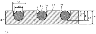
도 6 은, 실시예의 이방성 도전 필름 (1b) 의 단면도이다.
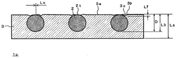
도 7 은, 실시예의 이방성 도전 필름 (1c) 의 단면도이다.
도 8 은, 실시예의 이방성 도전 필름 (1d) 의 단면도이다.
도 9 는, 실시예의 이방성 도전 필름 (1e) 의 단면도이다.
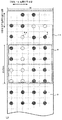
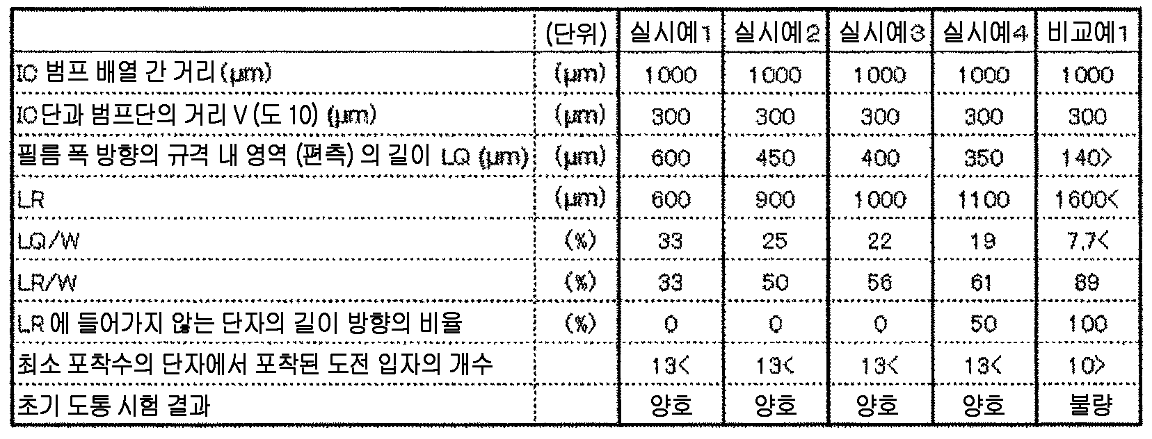
도 10 은, 평가용 IC 의 범프 배열을 나타내는 개략도이다.


1P : 이방성 도전 필름의 폭 방향의 폭의 단부
2, 2a, 2b, 2c, 2d : 도전 입자
2t : 도전 입자의 정부
2X : 도전 입자의 누락
2Y : 누락이 연속하고 있는 부분
3 : 절연성 수지 바인더
3a : 인접하는 도전 입자 간의 중앙부에 있어서의 절연성 수지 바인더의 표면
3b, 3c : 함몰
3p : 접평면
4 : 절연성 접착층
5 : 반복 유닛
10 : 범프, 단자
11 : 단자열
12 : 전자 부품
D : 도전 입자의 평균 입자경
L1 : 격자축
La : 절연성 수지 바인더의 두께
Q : 규격 내 영역
R : 규격 외 지점을 포함하는 영역
S : 임의의 영역
Claims (10)
- 절연성 수지 바인더에 도전 입자가 규칙적으로 배치되어 있는 규칙 배치 영역을 갖는, 길이가 5 m 이상인 이방성 도전 필름으로서, 상기 규칙 배치 영역 내에, 도전 입자가 연속하여 소정수 이상 누락되어 있는 지점이 존재하지 않는 규격 내 영역이, 이방성 도전 필름의 폭 방향의 소정 폭으로, 이방성 도전 필름의 길이 방향으로 소정 길이 이상으로 존재하는, 이방성 도전 필름.
- 제 1 항에 있어서,
상기 규칙 배치 영역과 상기 규격 내 영역이 일치하고 있는, 이방성 도전 필름. - 제 1 항에 있어서,
도전 입자가 연속하여 소정수 이상 누락되어 있는 지점인 규격 외 지점이 존재하는, 이방성 도전 필름. - 제 1 항 내지 제 3 항 중 어느 한 항에 있어서,
이방성 도전 필름의 전체폭으로 길이 방향 200 ㎛ 의 임의로 선택한 영역에 있어서, 도전 입자가 10 개 이상 존재하는, 이방성 도전 필름. - 제 1 항 내지 제 4 항 중 어느 한 항에 있어서,
이방성 도전 필름의 폭 방향의 적어도 단부 영역을 따라 규격 내 영역을 갖는, 이방성 도전 필름. - 제 1 항 내지 제 5 항 중 어느 한 항에 있어서,
이방성 도전 필름이 릴에 감긴 권장체인, 이방성 도전 필름. - 절연성 수지 바인더에 도전 입자가 규칙적으로 배치되어 있는 이방성 도전 필름의 광폭 원단을, 규칙적인 배치에 대해 도전 입자가 연속하여 소정수 이상 누락되어 있는 규격 외 지점이 포함되지 않도록, 혹은 규격 외 지점이 필름의 폭 방향의 의도한 위치가 되도록, 길이 방향으로 재단하여, 길이 5 m 이상의 이방성 도전 필름으로 하는, 이방성 도전 필름의 제조 방법.
- 절연성 수지 바인더에 도전 입자가 규칙적으로 배치되어 있는 규격 배치 영역을 갖는 이방성 도전 필름으로부터, 도전 입자가 연속하여 소정수 이상 누락되어 있는 규격 외 지점을 제거하고, 제거 후의 이방성 도전 필름을 연결하여, 길이 5 m 이상의 이방성 도전 필름으로 하는, 이방성 도전 필름의 제조 방법.
- 단자열을 갖는 제 1 전자 부품과 단자열을 갖는 제 2 전자 부품을, 절연성 수지 바인더에 도전 입자가 규칙적으로 배치되어 있는 규격 배치 영역을 갖는 이방성 도전 필름을 개재하여 열압착함으로써 제 1 전자 부품과 제 2 전자 부품의 단자열끼리를 이방성 도전 접속하는 접속 구조체의 제조 방법으로서,
이방성 도전 필름으로서, 상기 규격 배치 영역 내에, 도전 입자가 연속하여 소정수 이상 누락되어 있는 지점이 존재하지 않는 규격 내 영역이, 이방성 도전 필름의 폭 방향의 소정 폭으로 이방성 도전 필름의 길이 방향으로 소정 길이로 형성되어 있는 이방성 도전 필름을 사용하고,
상기 규격 내 영역을 전자 부품의 단자열에 얼라인먼트하는, 접속 구조체의 제조 방법. - 제 9 항에 있어서,
제 1 전자 부품 및 제 2 전자 부품이 각각 복수의 단자열을 갖고, 이방성 도전 필름에 규격 내 영역이 병렬하여 형성되어 있는 경우에,
이웃하는 규격 영역 사이의 영역을, 단자열과 단자열 사이의 영역에 얼라인먼트하는, 접속 구조체의 제조 방법.
Priority Applications (1)
| Application Number | Priority Date | Filing Date | Title |
|---|---|---|---|
| KR1020207024477A KR102308962B1 (ko) | 2016-05-05 | 2017-04-24 | 이방성 도전 필름 |
Applications Claiming Priority (5)
| Application Number | Priority Date | Filing Date | Title |
|---|---|---|---|
| JPJP-P-2016-092901 | 2016-05-05 | ||
| JP2016092901 | 2016-05-05 | ||
| JPJP-P-2017-084914 | 2017-04-23 | ||
| JP2017084914A JP7095227B2 (ja) | 2016-05-05 | 2017-04-23 | 異方性導電フィルム |
| PCT/JP2017/016245 WO2017191774A1 (ja) | 2016-05-05 | 2017-04-24 | 異方性導電フィルム |
Related Child Applications (1)
| Application Number | Title | Priority Date | Filing Date |
|---|---|---|---|
| KR1020207024477A Division KR102308962B1 (ko) | 2016-05-05 | 2017-04-24 | 이방성 도전 필름 |
Publications (2)
| Publication Number | Publication Date |
|---|---|
| KR20180098356A true KR20180098356A (ko) | 2018-09-03 |
| KR102149964B1 KR102149964B1 (ko) | 2020-08-31 |
Family
ID=60203559
Family Applications (4)
| Application Number | Title | Priority Date | Filing Date |
|---|---|---|---|
| KR1020217031177A Active KR102502795B1 (ko) | 2016-05-05 | 2017-04-24 | 이방성 도전 필름 |
| KR1020237005740A Active KR102621211B1 (ko) | 2016-05-05 | 2017-04-24 | 이방성 도전 필름 |
| KR1020187021397A Active KR102149964B1 (ko) | 2016-05-05 | 2017-04-24 | 이방성 도전 필름 |
| KR1020207024477A Active KR102308962B1 (ko) | 2016-05-05 | 2017-04-24 | 이방성 도전 필름 |
Family Applications Before (2)
| Application Number | Title | Priority Date | Filing Date |
|---|---|---|---|
| KR1020217031177A Active KR102502795B1 (ko) | 2016-05-05 | 2017-04-24 | 이방성 도전 필름 |
| KR1020237005740A Active KR102621211B1 (ko) | 2016-05-05 | 2017-04-24 | 이방성 도전 필름 |
Family Applications After (1)
| Application Number | Title | Priority Date | Filing Date |
|---|---|---|---|
| KR1020207024477A Active KR102308962B1 (ko) | 2016-05-05 | 2017-04-24 | 이방성 도전 필름 |
Country Status (6)
| Country | Link |
|---|---|
| US (2) | US10553554B2 (ko) |
| JP (3) | JP7095227B2 (ko) |
| KR (4) | KR102502795B1 (ko) |
| CN (1) | CN109075471B (ko) |
| TW (2) | TWI764821B (ko) |
| WO (1) | WO2017191774A1 (ko) |
Families Citing this family (10)
| Publication number | Priority date | Publication date | Assignee | Title |
|---|---|---|---|---|
| TWI785642B (zh) * | 2014-11-17 | 2022-12-01 | 日商迪睿合股份有限公司 | 異向性導電膜及連接構造體 |
| WO2017191772A1 (ja) * | 2016-05-05 | 2017-11-09 | デクセリアルズ株式会社 | フィラー配置フィルム |
| JP7095227B2 (ja) * | 2016-05-05 | 2022-07-05 | デクセリアルズ株式会社 | 異方性導電フィルム |
| US11013126B2 (en) * | 2016-12-01 | 2021-05-18 | Dexerials Corporation | Connection structure |
| CN112823448B (zh) * | 2018-10-31 | 2023-05-23 | 迪睿合株式会社 | 连接体的制备方法、各向异性接合薄膜、连接体 |
| KR20210018700A (ko) * | 2019-08-09 | 2021-02-18 | 삼성디스플레이 주식회사 | 접착 부재 및 이를 포함한 표시장치 |
| KR102888155B1 (ko) * | 2019-12-23 | 2025-11-19 | 엘지디스플레이 주식회사 | 표시 장치 및 상기 표시 장치를 제조하기 위한 방법 |
| WO2021161935A1 (ja) | 2020-02-12 | 2021-08-19 | デクセリアルズ株式会社 | 異方性導電フィルム |
| JP7705020B2 (ja) * | 2020-02-12 | 2025-07-09 | デクセリアルズ株式会社 | 異方性導電フィルム |
| JP2023117329A (ja) | 2022-02-10 | 2023-08-23 | デクセリアルズ株式会社 | 導電フィルムの設計方法 |
Citations (11)
| Publication number | Priority date | Publication date | Assignee | Title |
|---|---|---|---|---|
| JPS5147048B1 (ko) | 1967-11-30 | 1976-12-13 | ||
| JPH07243798A (ja) * | 1994-03-02 | 1995-09-19 | Masahiro Yuasa | クレー射撃用屋外表示盤 |
| KR20050070713A (ko) * | 2003-12-30 | 2005-07-07 | 엘지.필립스 엘시디 주식회사 | 이방성 도전필름 절단장치 및 그 절단방법 |
| KR20070023104A (ko) * | 2005-08-23 | 2007-02-28 | 주식회사 프리텍 | 이방성도전 필름 본딩장치 |
| KR20080009043A (ko) * | 2004-11-09 | 2008-01-24 | 보드 오브 리전츠, 더 유니버시티 오브 텍사스 시스템 | 나노섬유 리본과 시트 및 트위스트 및 논-트위스트나노섬유 방적사의 제조 및 애플리케이션 |
| JP2010251337A (ja) * | 2010-08-05 | 2010-11-04 | Sony Chemical & Information Device Corp | 異方性導電膜及びその製造方法並びに接続構造体 |
| JP4887700B2 (ja) | 2005-09-09 | 2012-02-29 | 住友ベークライト株式会社 | 異方導電性フィルムおよび電子・電機機器 |
| JP2016066573A (ja) * | 2013-11-19 | 2016-04-28 | デクセリアルズ株式会社 | 異方導電性フィルム及び接続構造体 |
| KR20170113039A (ko) * | 2016-03-25 | 2017-10-12 | 데쿠세리아루즈 가부시키가이샤 | 전자 부품, 접속체, 전자 부품의 설계 방법 |
| KR20170135919A (ko) * | 2015-05-27 | 2017-12-08 | 데쿠세리아루즈 가부시키가이샤 | 이방 도전성 필름 및 접속 구조체 |
| KR20180098607A (ko) * | 2016-05-05 | 2018-09-04 | 데쿠세리아루즈 가부시키가이샤 | 이방성 도전 필름 |
Family Cites Families (15)
| Publication number | Priority date | Publication date | Assignee | Title |
|---|---|---|---|---|
| WO2000033374A1 (fr) * | 1998-12-02 | 2000-06-08 | Seiko Epson Corporation | Couche conductrice anisotrope, puce a semi-conducteur et procede de conditionnement |
| JP4130747B2 (ja) | 2002-03-28 | 2008-08-06 | 旭化成エレクトロニクス株式会社 | 異方導電性接着シートおよびその製造方法 |
| CN101233655B (zh) * | 2005-08-04 | 2010-08-18 | 日立化成工业株式会社 | 各向异性导电膜及其制造方法 |
| JP5388572B2 (ja) * | 2006-04-27 | 2014-01-15 | デクセリアルズ株式会社 | 導電粒子配置シート及び異方導電性フィルム |
| JP5147048B2 (ja) | 2007-07-25 | 2013-02-20 | 旭化成イーマテリアルズ株式会社 | 異方導電性フィルム |
| JP2009152160A (ja) * | 2007-12-25 | 2009-07-09 | Tokai Rubber Ind Ltd | 粒子転写型およびその製造方法、粒子転写膜の製造方法ならびに異方性導電膜 |
| JP2011029207A (ja) * | 2010-11-02 | 2011-02-10 | Sony Chemical & Information Device Corp | フィルム積層体、フィルム積層体の貼付方法、フィルム積層体を用いた接続方法及び接続構造体 |
| US9102851B2 (en) | 2011-09-15 | 2015-08-11 | Trillion Science, Inc. | Microcavity carrier belt and method of manufacture |
| JP6185742B2 (ja) * | 2013-04-19 | 2017-08-23 | デクセリアルズ株式会社 | 異方性導電フィルム、接続方法、及び接合体 |
| JP6151597B2 (ja) * | 2013-07-29 | 2017-06-21 | デクセリアルズ株式会社 | 導電性接着フィルムの製造方法、導電性接着フィルム、接続体の製造方法 |
| JP6289831B2 (ja) | 2013-07-29 | 2018-03-07 | デクセリアルズ株式会社 | 導電性接着フィルムの製造方法、導電性接着フィルム、接続体の製造方法 |
| CN110499119B (zh) * | 2013-11-19 | 2023-07-18 | 迪睿合株式会社 | 各向异性导电性膜及连接构造体 |
| JP6645730B2 (ja) * | 2014-01-28 | 2020-02-14 | デクセリアルズ株式会社 | 接続体及び接続体の製造方法 |
| CN104698689B (zh) * | 2015-04-07 | 2017-07-14 | 京东方科技集团股份有限公司 | 一种各向异性导电胶膜、显示装置及其返修方法 |
| JP7095227B2 (ja) * | 2016-05-05 | 2022-07-05 | デクセリアルズ株式会社 | 異方性導電フィルム |
-
2017
- 2017-04-23 JP JP2017084914A patent/JP7095227B2/ja active Active
- 2017-04-24 US US16/096,255 patent/US10553554B2/en active Active
- 2017-04-24 KR KR1020217031177A patent/KR102502795B1/ko active Active
- 2017-04-24 KR KR1020237005740A patent/KR102621211B1/ko active Active
- 2017-04-24 KR KR1020187021397A patent/KR102149964B1/ko active Active
- 2017-04-24 WO PCT/JP2017/016245 patent/WO2017191774A1/ja not_active Ceased
- 2017-04-24 CN CN201780025075.7A patent/CN109075471B/zh active Active
- 2017-04-24 KR KR1020207024477A patent/KR102308962B1/ko active Active
- 2017-05-01 TW TW110132350A patent/TWI764821B/zh active
- 2017-05-01 TW TW106114400A patent/TWI740934B/zh active
-
2019
- 2019-12-27 US US16/728,554 patent/US10714444B2/en active Active
-
2022
- 2022-06-21 JP JP2022099633A patent/JP7788950B2/ja active Active
-
2025
- 2025-10-31 JP JP2025184149A patent/JP2026009264A/ja active Pending
Patent Citations (11)
| Publication number | Priority date | Publication date | Assignee | Title |
|---|---|---|---|---|
| JPS5147048B1 (ko) | 1967-11-30 | 1976-12-13 | ||
| JPH07243798A (ja) * | 1994-03-02 | 1995-09-19 | Masahiro Yuasa | クレー射撃用屋外表示盤 |
| KR20050070713A (ko) * | 2003-12-30 | 2005-07-07 | 엘지.필립스 엘시디 주식회사 | 이방성 도전필름 절단장치 및 그 절단방법 |
| KR20080009043A (ko) * | 2004-11-09 | 2008-01-24 | 보드 오브 리전츠, 더 유니버시티 오브 텍사스 시스템 | 나노섬유 리본과 시트 및 트위스트 및 논-트위스트나노섬유 방적사의 제조 및 애플리케이션 |
| KR20070023104A (ko) * | 2005-08-23 | 2007-02-28 | 주식회사 프리텍 | 이방성도전 필름 본딩장치 |
| JP4887700B2 (ja) | 2005-09-09 | 2012-02-29 | 住友ベークライト株式会社 | 異方導電性フィルムおよび電子・電機機器 |
| JP2010251337A (ja) * | 2010-08-05 | 2010-11-04 | Sony Chemical & Information Device Corp | 異方性導電膜及びその製造方法並びに接続構造体 |
| JP2016066573A (ja) * | 2013-11-19 | 2016-04-28 | デクセリアルズ株式会社 | 異方導電性フィルム及び接続構造体 |
| KR20170135919A (ko) * | 2015-05-27 | 2017-12-08 | 데쿠세리아루즈 가부시키가이샤 | 이방 도전성 필름 및 접속 구조체 |
| KR20170113039A (ko) * | 2016-03-25 | 2017-10-12 | 데쿠세리아루즈 가부시키가이샤 | 전자 부품, 접속체, 전자 부품의 설계 방법 |
| KR20180098607A (ko) * | 2016-05-05 | 2018-09-04 | 데쿠세리아루즈 가부시키가이샤 | 이방성 도전 필름 |
Also Published As
| Publication number | Publication date |
|---|---|
| CN109075471B (zh) | 2021-03-12 |
| WO2017191774A1 (ja) | 2017-11-09 |
| JP7095227B2 (ja) | 2022-07-05 |
| TW201816029A (zh) | 2018-05-01 |
| JP2026009264A (ja) | 2026-01-19 |
| TWI740934B (zh) | 2021-10-01 |
| CN109075471A (zh) | 2018-12-21 |
| KR20210122900A (ko) | 2021-10-12 |
| US20200144214A1 (en) | 2020-05-07 |
| JP2022118147A (ja) | 2022-08-12 |
| KR20230030025A (ko) | 2023-03-03 |
| TW202202584A (zh) | 2022-01-16 |
| KR20200103874A (ko) | 2020-09-02 |
| KR102502795B1 (ko) | 2023-02-23 |
| KR102308962B1 (ko) | 2021-10-06 |
| JP7788950B2 (ja) | 2025-12-19 |
| TWI764821B (zh) | 2022-05-11 |
| JP2017204461A (ja) | 2017-11-16 |
| KR102621211B1 (ko) | 2024-01-04 |
| US10714444B2 (en) | 2020-07-14 |
| US10553554B2 (en) | 2020-02-04 |
| US20190139927A1 (en) | 2019-05-09 |
| KR102149964B1 (ko) | 2020-08-31 |
Similar Documents
| Publication | Publication Date | Title |
|---|---|---|
| KR20180098356A (ko) | 이방성 도전 필름 | |
| KR102243340B1 (ko) | 이방성 도전 필름 | |
| KR102228112B1 (ko) | 이방성 도전 필름 | |
| KR20190016571A (ko) | 필러 함유 필름 | |
| WO2018101138A1 (ja) | 接続構造体 | |
| KR20190038603A (ko) | 필러 함유 필름 | |
| CN112534650A (zh) | 各向异性导电薄膜 | |
| WO2017191779A1 (ja) | 異方性導電フィルム | |
| CN109964371B (zh) | 各向异性导电膜 | |
| TW202209356A (zh) | 異向性導電膜 | |
| HK1261545A1 (en) | Anisotropic conductive film | |
| HK40064112A (en) | Anisotropic conductive film | |
| HK40050768A (en) | Anisotropic electroconductive film | |
| HK1261545B (zh) | 各向异性导电膜 | |
| HK1261541A1 (en) | Anisotropic electroconductive film | |
| HK40008173A (en) | Anisotropic conductive film | |
| HK40001200A (en) | Anisotropic conductive film |
Legal Events
| Date | Code | Title | Description |
|---|---|---|---|
| A201 | Request for examination | ||
| PA0105 | International application |
Patent event date: 20180724 Patent event code: PA01051R01D Comment text: International Patent Application |
|
| PA0201 | Request for examination |
Patent event code: PA02012R01D Patent event date: 20180724 Comment text: Request for Examination of Application |
|
| PG1501 | Laying open of application | ||
| E902 | Notification of reason for refusal | ||
| PE0902 | Notice of grounds for rejection |
Comment text: Notification of reason for refusal Patent event date: 20190819 Patent event code: PE09021S01D |
|
| E701 | Decision to grant or registration of patent right | ||
| PE0701 | Decision of registration |
Patent event code: PE07011S01D Comment text: Decision to Grant Registration Patent event date: 20200522 |
|
| A107 | Divisional application of patent | ||
| GRNT | Written decision to grant | ||
| PA0104 | Divisional application for international application |
Comment text: Divisional Application for International Patent Patent event code: PA01041R01D Patent event date: 20200825 |
|
| PR0701 | Registration of establishment |
Comment text: Registration of Establishment Patent event date: 20200825 Patent event code: PR07011E01D |
|
| PR1002 | Payment of registration fee |
Payment date: 20200826 End annual number: 3 Start annual number: 1 |
|
| PG1601 | Publication of registration | ||
| PR1001 | Payment of annual fee |
Payment date: 20230718 Start annual number: 4 End annual number: 4 |
|
| PR1001 | Payment of annual fee |
Payment date: 20240725 Start annual number: 5 End annual number: 5 |