KR20180098607A - 이방성 도전 필름 - Google Patents
이방성 도전 필름 Download PDFInfo
- Publication number
- KR20180098607A KR20180098607A KR1020187021398A KR20187021398A KR20180098607A KR 20180098607 A KR20180098607 A KR 20180098607A KR 1020187021398 A KR1020187021398 A KR 1020187021398A KR 20187021398 A KR20187021398 A KR 20187021398A KR 20180098607 A KR20180098607 A KR 20180098607A
- Authority
- KR
- South Korea
- Prior art keywords
- conductive particles
- anisotropic conductive
- conductive film
- repeating unit
- conductive
- Prior art date
- Legal status (The legal status is an assumption and is not a legal conclusion. Google has not performed a legal analysis and makes no representation as to the accuracy of the status listed.)
- Granted
Links
Images


Classifications
-
- H—ELECTRICITY
- H01—ELECTRIC ELEMENTS
- H01B—CABLES; CONDUCTORS; INSULATORS; SELECTION OF MATERIALS FOR THEIR CONDUCTIVE, INSULATING OR DIELECTRIC PROPERTIES
- H01B5/00—Non-insulated conductors or conductive bodies characterised by their form
- H01B5/16—Non-insulated conductors or conductive bodies characterised by their form comprising conductive material in insulating or poorly conductive material, e.g. conductive rubber
-
- B—PERFORMING OPERATIONS; TRANSPORTING
- B32—LAYERED PRODUCTS
- B32B—LAYERED PRODUCTS, i.e. PRODUCTS BUILT-UP OF STRATA OF FLAT OR NON-FLAT, e.g. CELLULAR OR HONEYCOMB, FORM
- B32B27/00—Layered products comprising a layer of synthetic resin
- B32B27/18—Layered products comprising a layer of synthetic resin characterised by the use of special additives
- B32B27/20—Layered products comprising a layer of synthetic resin characterised by the use of special additives using fillers, pigments, thixotroping agents
-
- B—PERFORMING OPERATIONS; TRANSPORTING
- B32—LAYERED PRODUCTS
- B32B—LAYERED PRODUCTS, i.e. PRODUCTS BUILT-UP OF STRATA OF FLAT OR NON-FLAT, e.g. CELLULAR OR HONEYCOMB, FORM
- B32B5/00—Layered products characterised by the non- homogeneity or physical structure, i.e. comprising a fibrous, filamentary, particulate or foam layer; Layered products characterised by having a layer differing constitutionally or physically in different parts
- B32B5/16—Layered products characterised by the non- homogeneity or physical structure, i.e. comprising a fibrous, filamentary, particulate or foam layer; Layered products characterised by having a layer differing constitutionally or physically in different parts characterised by features of a layer formed of particles, e.g. chips, powder or granules
-
- C—CHEMISTRY; METALLURGY
- C09—DYES; PAINTS; POLISHES; NATURAL RESINS; ADHESIVES; COMPOSITIONS NOT OTHERWISE PROVIDED FOR; APPLICATIONS OF MATERIALS NOT OTHERWISE PROVIDED FOR
- C09J—ADHESIVES; NON-MECHANICAL ASPECTS OF ADHESIVE PROCESSES IN GENERAL; ADHESIVE PROCESSES NOT PROVIDED FOR ELSEWHERE; USE OF MATERIALS AS ADHESIVES
- C09J7/00—Adhesives in the form of films or foils
- C09J7/10—Adhesives in the form of films or foils without carriers
-
- C—CHEMISTRY; METALLURGY
- C09—DYES; PAINTS; POLISHES; NATURAL RESINS; ADHESIVES; COMPOSITIONS NOT OTHERWISE PROVIDED FOR; APPLICATIONS OF MATERIALS NOT OTHERWISE PROVIDED FOR
- C09J—ADHESIVES; NON-MECHANICAL ASPECTS OF ADHESIVE PROCESSES IN GENERAL; ADHESIVE PROCESSES NOT PROVIDED FOR ELSEWHERE; USE OF MATERIALS AS ADHESIVES
- C09J9/00—Adhesives characterised by their physical nature or the effects produced, e.g. glue sticks
- C09J9/02—Electrically-conducting adhesives
-
- H—ELECTRICITY
- H01—ELECTRIC ELEMENTS
- H01B—CABLES; CONDUCTORS; INSULATORS; SELECTION OF MATERIALS FOR THEIR CONDUCTIVE, INSULATING OR DIELECTRIC PROPERTIES
- H01B1/00—Conductors or conductive bodies characterised by the conductive materials; Selection of materials as conductors
- H01B1/20—Conductive material dispersed in non-conductive organic material
- H01B1/22—Conductive material dispersed in non-conductive organic material the conductive material comprising metals or alloys
-
- H—ELECTRICITY
- H01—ELECTRIC ELEMENTS
- H01R—ELECTRICALLY-CONDUCTIVE CONNECTIONS; STRUCTURAL ASSOCIATIONS OF A PLURALITY OF MUTUALLY-INSULATED ELECTRICAL CONNECTING ELEMENTS; COUPLING DEVICES; CURRENT COLLECTORS
- H01R11/00—Individual connecting elements providing two or more spaced connecting locations for conductive members which are, or may be, thereby interconnected, e.g. end pieces for wires or cables supported by the wire or cable and having means for facilitating electrical connection to some other wire, terminal, or conductive member, blocks of binding posts
- H01R11/01—Individual connecting elements providing two or more spaced connecting locations for conductive members which are, or may be, thereby interconnected, e.g. end pieces for wires or cables supported by the wire or cable and having means for facilitating electrical connection to some other wire, terminal, or conductive member, blocks of binding posts characterised by the form or arrangement of the conductive interconnection between the connecting locations
-
- H—ELECTRICITY
- H01—ELECTRIC ELEMENTS
- H01R—ELECTRICALLY-CONDUCTIVE CONNECTIONS; STRUCTURAL ASSOCIATIONS OF A PLURALITY OF MUTUALLY-INSULATED ELECTRICAL CONNECTING ELEMENTS; COUPLING DEVICES; CURRENT COLLECTORS
- H01R43/00—Apparatus or processes specially adapted for manufacturing, assembling, maintaining, or repairing of line connectors or current collectors or for joining electric conductors
-
- B—PERFORMING OPERATIONS; TRANSPORTING
- B32—LAYERED PRODUCTS
- B32B—LAYERED PRODUCTS, i.e. PRODUCTS BUILT-UP OF STRATA OF FLAT OR NON-FLAT, e.g. CELLULAR OR HONEYCOMB, FORM
- B32B2260/00—Layered product comprising an impregnated, embedded, or bonded layer wherein the layer comprises an impregnation, embedding, or binder material
- B32B2260/02—Composition of the impregnated, bonded or embedded layer
- B32B2260/025—Particulate layer
-
- B—PERFORMING OPERATIONS; TRANSPORTING
- B32—LAYERED PRODUCTS
- B32B—LAYERED PRODUCTS, i.e. PRODUCTS BUILT-UP OF STRATA OF FLAT OR NON-FLAT, e.g. CELLULAR OR HONEYCOMB, FORM
- B32B2260/00—Layered product comprising an impregnated, embedded, or bonded layer wherein the layer comprises an impregnation, embedding, or binder material
- B32B2260/04—Impregnation, embedding, or binder material
- B32B2260/046—Synthetic resin
-
- C—CHEMISTRY; METALLURGY
- C08—ORGANIC MACROMOLECULAR COMPOUNDS; THEIR PREPARATION OR CHEMICAL WORKING-UP; COMPOSITIONS BASED THEREON
- C08K—Use of inorganic or non-macromolecular organic substances as compounding ingredients
- C08K2201/00—Specific properties of additives
- C08K2201/001—Conductive additives
-
- C—CHEMISTRY; METALLURGY
- C09—DYES; PAINTS; POLISHES; NATURAL RESINS; ADHESIVES; COMPOSITIONS NOT OTHERWISE PROVIDED FOR; APPLICATIONS OF MATERIALS NOT OTHERWISE PROVIDED FOR
- C09J—ADHESIVES; NON-MECHANICAL ASPECTS OF ADHESIVE PROCESSES IN GENERAL; ADHESIVE PROCESSES NOT PROVIDED FOR ELSEWHERE; USE OF MATERIALS AS ADHESIVES
- C09J2203/00—Applications of adhesives in processes or use of adhesives in the form of films or foils
- C09J2203/326—Applications of adhesives in processes or use of adhesives in the form of films or foils for bonding electronic components such as wafers, chips or semiconductors
-
- C—CHEMISTRY; METALLURGY
- C09—DYES; PAINTS; POLISHES; NATURAL RESINS; ADHESIVES; COMPOSITIONS NOT OTHERWISE PROVIDED FOR; APPLICATIONS OF MATERIALS NOT OTHERWISE PROVIDED FOR
- C09J—ADHESIVES; NON-MECHANICAL ASPECTS OF ADHESIVE PROCESSES IN GENERAL; ADHESIVE PROCESSES NOT PROVIDED FOR ELSEWHERE; USE OF MATERIALS AS ADHESIVES
- C09J2301/00—Additional features of adhesives in the form of films or foils
- C09J2301/30—Additional features of adhesives in the form of films or foils characterized by the chemical, physicochemical or physical properties of the adhesive or the carrier
- C09J2301/304—Additional features of adhesives in the form of films or foils characterized by the chemical, physicochemical or physical properties of the adhesive or the carrier the adhesive being heat-activatable, i.e. not tacky at temperatures inferior to 30°C
-
- C—CHEMISTRY; METALLURGY
- C09—DYES; PAINTS; POLISHES; NATURAL RESINS; ADHESIVES; COMPOSITIONS NOT OTHERWISE PROVIDED FOR; APPLICATIONS OF MATERIALS NOT OTHERWISE PROVIDED FOR
- C09J—ADHESIVES; NON-MECHANICAL ASPECTS OF ADHESIVE PROCESSES IN GENERAL; ADHESIVE PROCESSES NOT PROVIDED FOR ELSEWHERE; USE OF MATERIALS AS ADHESIVES
- C09J2301/00—Additional features of adhesives in the form of films or foils
- C09J2301/30—Additional features of adhesives in the form of films or foils characterized by the chemical, physicochemical or physical properties of the adhesive or the carrier
- C09J2301/314—Additional features of adhesives in the form of films or foils characterized by the chemical, physicochemical or physical properties of the adhesive or the carrier the adhesive layer and/or the carrier being conductive
-
- C—CHEMISTRY; METALLURGY
- C09—DYES; PAINTS; POLISHES; NATURAL RESINS; ADHESIVES; COMPOSITIONS NOT OTHERWISE PROVIDED FOR; APPLICATIONS OF MATERIALS NOT OTHERWISE PROVIDED FOR
- C09J—ADHESIVES; NON-MECHANICAL ASPECTS OF ADHESIVE PROCESSES IN GENERAL; ADHESIVE PROCESSES NOT PROVIDED FOR ELSEWHERE; USE OF MATERIALS AS ADHESIVES
- C09J2301/00—Additional features of adhesives in the form of films or foils
- C09J2301/40—Additional features of adhesives in the form of films or foils characterized by the presence of essential components
- C09J2301/408—Additional features of adhesives in the form of films or foils characterized by the presence of essential components additives as essential feature of the adhesive layer
-
- H—ELECTRICITY
- H10—SEMICONDUCTOR DEVICES; ELECTRIC SOLID-STATE DEVICES NOT OTHERWISE PROVIDED FOR
- H10W—GENERIC PACKAGES, INTERCONNECTIONS, CONNECTORS OR OTHER CONSTRUCTIONAL DETAILS OF DEVICES COVERED BY CLASS H10
- H10W72/00—Interconnections or connectors in packages
- H10W72/01—Manufacture or treatment
- H10W72/013—Manufacture or treatment of die-attach connectors
- H10W72/01321—Manufacture or treatment of die-attach connectors using local deposition
- H10W72/01323—Manufacture or treatment of die-attach connectors using local deposition in liquid form, e.g. by dispensing droplets or by screen printing
-
- H—ELECTRICITY
- H10—SEMICONDUCTOR DEVICES; ELECTRIC SOLID-STATE DEVICES NOT OTHERWISE PROVIDED FOR
- H10W—GENERIC PACKAGES, INTERCONNECTIONS, CONNECTORS OR OTHER CONSTRUCTIONAL DETAILS OF DEVICES COVERED BY CLASS H10
- H10W72/00—Interconnections or connectors in packages
- H10W72/01—Manufacture or treatment
- H10W72/013—Manufacture or treatment of die-attach connectors
- H10W72/01331—Manufacture or treatment of die-attach connectors using blanket deposition
- H10W72/01336—Manufacture or treatment of die-attach connectors using blanket deposition in solid form, e.g. by using a powder or by laminating a foil
-
- H—ELECTRICITY
- H10—SEMICONDUCTOR DEVICES; ELECTRIC SOLID-STATE DEVICES NOT OTHERWISE PROVIDED FOR
- H10W—GENERIC PACKAGES, INTERCONNECTIONS, CONNECTORS OR OTHER CONSTRUCTIONAL DETAILS OF DEVICES COVERED BY CLASS H10
- H10W72/00—Interconnections or connectors in packages
- H10W72/071—Connecting or disconnecting
- H10W72/073—Connecting or disconnecting of die-attach connectors
- H10W72/07331—Connecting techniques
- H10W72/07332—Compression bonding, e.g. thermocompression bonding
-
- H—ELECTRICITY
- H10—SEMICONDUCTOR DEVICES; ELECTRIC SOLID-STATE DEVICES NOT OTHERWISE PROVIDED FOR
- H10W—GENERIC PACKAGES, INTERCONNECTIONS, CONNECTORS OR OTHER CONSTRUCTIONAL DETAILS OF DEVICES COVERED BY CLASS H10
- H10W72/00—Interconnections or connectors in packages
- H10W72/071—Connecting or disconnecting
- H10W72/074—Connecting or disconnecting of anisotropic conductive adhesives
-
- H—ELECTRICITY
- H10—SEMICONDUCTOR DEVICES; ELECTRIC SOLID-STATE DEVICES NOT OTHERWISE PROVIDED FOR
- H10W—GENERIC PACKAGES, INTERCONNECTIONS, CONNECTORS OR OTHER CONSTRUCTIONAL DETAILS OF DEVICES COVERED BY CLASS H10
- H10W72/00—Interconnections or connectors in packages
- H10W72/20—Bump connectors, e.g. solder bumps or copper pillars; Dummy bumps; Thermal bumps
- H10W72/251—Materials
-
- H—ELECTRICITY
- H10—SEMICONDUCTOR DEVICES; ELECTRIC SOLID-STATE DEVICES NOT OTHERWISE PROVIDED FOR
- H10W—GENERIC PACKAGES, INTERCONNECTIONS, CONNECTORS OR OTHER CONSTRUCTIONAL DETAILS OF DEVICES COVERED BY CLASS H10
- H10W72/00—Interconnections or connectors in packages
- H10W72/20—Bump connectors, e.g. solder bumps or copper pillars; Dummy bumps; Thermal bumps
- H10W72/261—Functions other than electrical connecting
-
- H—ELECTRICITY
- H10—SEMICONDUCTOR DEVICES; ELECTRIC SOLID-STATE DEVICES NOT OTHERWISE PROVIDED FOR
- H10W—GENERIC PACKAGES, INTERCONNECTIONS, CONNECTORS OR OTHER CONSTRUCTIONAL DETAILS OF DEVICES COVERED BY CLASS H10
- H10W72/00—Interconnections or connectors in packages
- H10W72/30—Die-attach connectors
- H10W72/321—Structures or relative sizes of die-attach connectors
- H10W72/322—Multilayered die-attach connectors, e.g. a coating on a top surface of a core
-
- H—ELECTRICITY
- H10—SEMICONDUCTOR DEVICES; ELECTRIC SOLID-STATE DEVICES NOT OTHERWISE PROVIDED FOR
- H10W—GENERIC PACKAGES, INTERCONNECTIONS, CONNECTORS OR OTHER CONSTRUCTIONAL DETAILS OF DEVICES COVERED BY CLASS H10
- H10W72/00—Interconnections or connectors in packages
- H10W72/30—Die-attach connectors
- H10W72/321—Structures or relative sizes of die-attach connectors
- H10W72/325—Die-attach connectors having a filler embedded in a matrix
-
- H—ELECTRICITY
- H10—SEMICONDUCTOR DEVICES; ELECTRIC SOLID-STATE DEVICES NOT OTHERWISE PROVIDED FOR
- H10W—GENERIC PACKAGES, INTERCONNECTIONS, CONNECTORS OR OTHER CONSTRUCTIONAL DETAILS OF DEVICES COVERED BY CLASS H10
- H10W72/00—Interconnections or connectors in packages
- H10W72/30—Die-attach connectors
- H10W72/351—Materials of die-attach connectors
- H10W72/352—Materials of die-attach connectors comprising metals or metalloids, e.g. solders
-
- H—ELECTRICITY
- H10—SEMICONDUCTOR DEVICES; ELECTRIC SOLID-STATE DEVICES NOT OTHERWISE PROVIDED FOR
- H10W—GENERIC PACKAGES, INTERCONNECTIONS, CONNECTORS OR OTHER CONSTRUCTIONAL DETAILS OF DEVICES COVERED BY CLASS H10
- H10W72/00—Interconnections or connectors in packages
- H10W72/30—Die-attach connectors
- H10W72/351—Materials of die-attach connectors
- H10W72/353—Materials of die-attach connectors not comprising solid metals or solid metalloids, e.g. ceramics
- H10W72/354—Materials of die-attach connectors not comprising solid metals or solid metalloids, e.g. ceramics comprising polymers
-
- H—ELECTRICITY
- H10—SEMICONDUCTOR DEVICES; ELECTRIC SOLID-STATE DEVICES NOT OTHERWISE PROVIDED FOR
- H10W—GENERIC PACKAGES, INTERCONNECTIONS, CONNECTORS OR OTHER CONSTRUCTIONAL DETAILS OF DEVICES COVERED BY CLASS H10
- H10W74/00—Encapsulations, e.g. protective coatings
- H10W74/10—Encapsulations, e.g. protective coatings characterised by their shape or disposition
- H10W74/15—Encapsulations, e.g. protective coatings characterised by their shape or disposition on active surfaces of flip-chip devices, e.g. underfills
-
- H—ELECTRICITY
- H10—SEMICONDUCTOR DEVICES; ELECTRIC SOLID-STATE DEVICES NOT OTHERWISE PROVIDED FOR
- H10W—GENERIC PACKAGES, INTERCONNECTIONS, CONNECTORS OR OTHER CONSTRUCTIONAL DETAILS OF DEVICES COVERED BY CLASS H10
- H10W90/00—Package configurations
- H10W90/701—Package configurations characterised by the relative positions of pads or connectors relative to package parts
- H10W90/721—Package configurations characterised by the relative positions of pads or connectors relative to package parts of bump connectors
- H10W90/724—Package configurations characterised by the relative positions of pads or connectors relative to package parts of bump connectors between a chip and a stacked insulating package substrate, interposer or RDL
-
- H—ELECTRICITY
- H10—SEMICONDUCTOR DEVICES; ELECTRIC SOLID-STATE DEVICES NOT OTHERWISE PROVIDED FOR
- H10W—GENERIC PACKAGES, INTERCONNECTIONS, CONNECTORS OR OTHER CONSTRUCTIONAL DETAILS OF DEVICES COVERED BY CLASS H10
- H10W90/00—Package configurations
- H10W90/701—Package configurations characterised by the relative positions of pads or connectors relative to package parts
- H10W90/731—Package configurations characterised by the relative positions of pads or connectors relative to package parts of die-attach connectors
- H10W90/734—Package configurations characterised by the relative positions of pads or connectors relative to package parts of die-attach connectors between a chip and a stacked insulating package substrate, interposer or RDL
Landscapes
- Chemical & Material Sciences (AREA)
- Organic Chemistry (AREA)
- Physics & Mathematics (AREA)
- Dispersion Chemistry (AREA)
- Spectroscopy & Molecular Physics (AREA)
- Engineering & Computer Science (AREA)
- Life Sciences & Earth Sciences (AREA)
- Wood Science & Technology (AREA)
- Manufacturing & Machinery (AREA)
- Non-Insulated Conductors (AREA)
- Manufacturing Of Electrical Connectors (AREA)
Abstract
Description
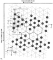
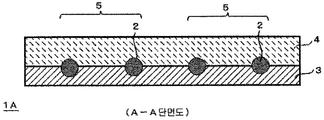
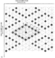
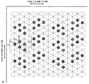
도 1b 는, 실시예의 이방성 도전 필름 (1A) 의 단면도이다.
도 2 는, 실시예의 이방성 도전 필름 (1B) 의 평면도이다.
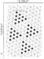
도 3 은, 실시예의 이방성 도전 필름 (1C) 의 평면도이다.
도 4 는, 실시예의 이방성 도전 필름 (1D) 의 평면도이다.
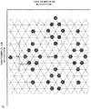
도 5 는, 실시예의 이방성 도전 필름 (1E) 의 평면도이다.
도 6 은, 실시예의 이방성 도전 필름 (1F) 의 평면도이다.
도 7 은, 실시예의 이방성 도전 필름 (1G) 의 평면도이다.
도 8 은, 실시예의 이방성 도전 필름 (1H) 의 평면도이다.
도 9 는, 실시예의 이방성 도전 필름 (1I) 의 평면도이다.
도 10 은, 실시예의 이방성 도전 필름 (1J) 의 평면도이다.
도 11 은, 실시예의 이방성 도전 필름 (1K) 의 평면도이다.
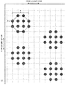
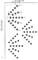
도 12 는, 실시예의 이방성 도전 필름 (1a) 의 단면도이다.
도 13 은, 실시예의 이방성 도전 필름 (1b) 의 단면도이다.
도 14 는, 실시예의 이방성 도전 필름 (1c) 의 단면도이다.
도 15 는, 실시예의 이방성 도전 필름 (1d) 의 단면도이다.
도 16 은, 실시예의 이방성 도전 필름 (1e) 의 단면도이다.


2, 2a, 2b, 2c, 2s : 도전 입자
2m, 2n, 2o, 2p, 2q, 2r : 도전 입자열
2t : 도전 입자의 정부
3 : 절연성 수지 바인더
3a : 절연성 수지 바인더의 표면
3b, 3c : 함몰
3P : 접평면
4 : 절연성 접착층
5, 5B : 반복 유닛
5a : 이방성 도전 필름의 길이 방향과 평행한 변
5b : 이방성 도전 필름의 폭 방향과 평행한 변
5x : 반복 유닛의 외형을 이루는 도전 입자의 중심을 순차 이어 형성되는 다각형
D : 평균 입자경
L1, L2 : 외접선
La : 절연성 수지 바인더의 두께
Lb : 도전 입자의 매립량
Lc : 도전 입자의 노출 부분의 직경
Ld : 함몰의 최대 직경
Le, Lf : 최대 깊이
Claims (12)
- 절연성 수지 바인더에 도전 입자가 배치된 이방성 도전 필름으로서,
도전 입자가 간격을 두고 일렬로 배열된 도전 입자열로서 도전 입자수가 상이한 것이 병렬하여 이루어지는 도전 입자의 반복 유닛이 반복 배치되어 있는, 이방성 도전 필름. - 제 1 항에 있어서,
반복 유닛이 이방성 도전 필름의 전체면에 걸쳐서 배치되어 있는, 이방성 도전 필름. - 제 1 항 또는 제 2 항에 있어서,
반복 유닛에 있어서 병렬하고 있는 도전 입자열을 구성하는 도전 입자수가 점차 상이한, 이방성 도전 필름. - 제 1 항 또는 제 2 항에 있어서,
반복 유닛에 있어서 병렬하고 있는 3 열의 도전 입자열에 있어서, 중앙의 도전 입자열을 구성하는 도전 입자수가 양측의 도전 입자열을 구성하는 도전 입자수보다 많거나 적은, 이방성 도전 필름. - 제 1 항 내지 제 4 항 중 어느 한 항에 있어서,
반복 유닛의 외형을 이루는 도전 입자의 중심을 순차 이어 형성되는 다각형의 각 변이 이방성 도전 필름의 길이 방향 또는 폭 방향과 사교하고 있는, 이방성 도전 필름. - 제 1 항 내지 제 4 항 중 어느 한 항에 있어서,
반복 유닛의 외형을 이루는 도전 입자의 중심을 순차 이어 형성되는 다각형이 이방성 도전 필름의 길이 방향 또는 폭 방향과 평행한 변을 갖는, 이방성 도전 필름. - 제 1 항 내지 제 6 항 중 어느 한 항에 있어서,
반복 유닛에 있어서, 도전 입자열끼리가 평행인, 이방성 도전 필름. - 제 1 항 내지 제 7 항 중 어느 한 항에 있어서,
반복 유닛과 함께 단독의 도전 입자가 반복 배치되어 있는, 이방성 도전 필름. - 제 1 항 내지 제 8 항 중 어느 한 항에 있어서,
반복 유닛 내에 있어서, 인접하는 도전 입자끼리의 최근접 거리가 도전 입자의 평균 입자경의 0.5 배 이상인, 이방성 도전 필름. - 제 1 항 내지 제 9 항 중 어느 한 항에 있어서,
반복 유닛을 구성하는 도전 입자가, 6 방 격자 또는 정방 격자의 각 격자점에 도전 입자가 존재하는 배치로부터, 소정의 격자점의 도전 입자를 규칙적으로 제거한 배치인, 이방성 도전 필름. - 제 1 항 내지 제 10 항 중 어느 한 항에 기재된 이방성 도전 필름에 의해 제 1 전자 부품과 제 2 전자 부품이 이방성 도전 접속되어 있는, 접속 구조체.
- 제 1 전자 부품과 제 2 전자 부품을 이방성 도전 필름을 개재하여 열압착함으로써 제 1 전자 부품과 제 2 전자 부품의 접속 구조체를 제조하는 방법으로서, 이방성 도전 필름으로서, 제 1 항 내지 제 10 항 중 어느 한 항에 기재된 이방성 도전 필름을 사용하는, 접속 구조체의 제조 방법.
Priority Applications (1)
| Application Number | Priority Date | Filing Date | Title |
|---|---|---|---|
| KR1020217011350A KR102682993B1 (ko) | 2016-05-05 | 2017-04-25 | 이방성 도전 필름 |
Applications Claiming Priority (5)
| Application Number | Priority Date | Filing Date | Title |
|---|---|---|---|
| JP2016092903 | 2016-05-05 | ||
| JPJP-P-2016-092903 | 2016-05-05 | ||
| JPJP-P-2017-085744 | 2017-04-24 | ||
| JP2017085744A JP7274811B2 (ja) | 2016-05-05 | 2017-04-24 | 異方性導電フィルム |
| PCT/JP2017/016345 WO2017191781A1 (ja) | 2016-05-05 | 2017-04-25 | 異方性導電フィルム |
Related Child Applications (1)
| Application Number | Title | Priority Date | Filing Date |
|---|---|---|---|
| KR1020217011350A Division KR102682993B1 (ko) | 2016-05-05 | 2017-04-25 | 이방성 도전 필름 |
Publications (2)
| Publication Number | Publication Date |
|---|---|
| KR20180098607A true KR20180098607A (ko) | 2018-09-04 |
| KR102243340B1 KR102243340B1 (ko) | 2021-04-22 |
Family
ID=60322404
Family Applications (1)
| Application Number | Title | Priority Date | Filing Date |
|---|---|---|---|
| KR1020187021398A Active KR102243340B1 (ko) | 2016-05-05 | 2017-04-25 | 이방성 도전 필름 |
Country Status (4)
| Country | Link |
|---|---|
| US (1) | US11794444B2 (ko) |
| JP (1) | JP7274811B2 (ko) |
| KR (1) | KR102243340B1 (ko) |
| CN (1) | CN109074894B (ko) |
Cited By (2)
| Publication number | Priority date | Publication date | Assignee | Title |
|---|---|---|---|---|
| KR20180098356A (ko) * | 2016-05-05 | 2018-09-03 | 데쿠세리아루즈 가부시키가이샤 | 이방성 도전 필름 |
| KR20180098355A (ko) * | 2016-05-05 | 2018-09-03 | 데쿠세리아루즈 가부시키가이샤 | 이방성 도전 필름 |
Families Citing this family (8)
| Publication number | Priority date | Publication date | Assignee | Title |
|---|---|---|---|---|
| WO2017191772A1 (ja) * | 2016-05-05 | 2017-11-09 | デクセリアルズ株式会社 | フィラー配置フィルム |
| US12550783B2 (en) | 2016-05-17 | 2026-02-10 | Taiwan Semiconductor Manufacturing Company, Ltd. | Device and method for UBM/RDL routing |
| KR102519126B1 (ko) * | 2018-03-30 | 2023-04-06 | 삼성디스플레이 주식회사 | 표시 장치 |
| CN112292430A (zh) * | 2018-06-06 | 2021-01-29 | 迪睿合株式会社 | 含有填料的膜 |
| CN112534650B (zh) | 2018-08-08 | 2023-05-23 | 迪睿合株式会社 | 各向异性导电薄膜 |
| KR102608245B1 (ko) * | 2019-01-21 | 2023-11-29 | 삼성전자주식회사 | 전기 전도성 복합막, 그 제조 방법, 이를 포함하는 이차전지와 전자기기 |
| WO2021161935A1 (ja) | 2020-02-12 | 2021-08-19 | デクセリアルズ株式会社 | 異方性導電フィルム |
| JP2023117329A (ja) | 2022-02-10 | 2023-08-23 | デクセリアルズ株式会社 | 導電フィルムの設計方法 |
Citations (8)
| Publication number | Priority date | Publication date | Assignee | Title |
|---|---|---|---|---|
| JPH09320345A (ja) | 1996-05-31 | 1997-12-12 | Whitaker Corp:The | 異方導電性フィルム |
| JP2002519473A (ja) | 1998-06-30 | 2002-07-02 | ミネソタ マイニング アンド マニュファクチャリング カンパニー | ファインピッチの異方導電性接着剤 |
| KR20080009043A (ko) * | 2004-11-09 | 2008-01-24 | 보드 오브 리전츠, 더 유니버시티 오브 텍사스 시스템 | 나노섬유 리본과 시트 및 트위스트 및 논-트위스트나노섬유 방적사의 제조 및 애플리케이션 |
| JP2009076431A (ja) * | 2007-01-31 | 2009-04-09 | Tokai Rubber Ind Ltd | 異方性導電膜およびその製造方法 |
| JP4887700B2 (ja) | 2005-09-09 | 2012-02-29 | 住友ベークライト株式会社 | 異方導電性フィルムおよび電子・電機機器 |
| JP2014063729A (ja) * | 2012-08-29 | 2014-04-10 | Dexerials Corp | 異方性導電フィルム及びその製造方法 |
| JP2016015205A (ja) * | 2014-06-30 | 2016-01-28 | デクセリアルズ株式会社 | 異方導電性フィルム及び接続構造体 |
| KR20170113039A (ko) * | 2016-03-25 | 2017-10-12 | 데쿠세리아루즈 가부시키가이샤 | 전자 부품, 접속체, 전자 부품의 설계 방법 |
Family Cites Families (15)
| Publication number | Priority date | Publication date | Assignee | Title |
|---|---|---|---|---|
| US4209481A (en) | 1976-04-19 | 1980-06-24 | Toray Industries, Inc. | Process for producing an anisotropically electroconductive sheet |
| JPS6032282B2 (ja) | 1976-09-09 | 1985-07-27 | 東レ株式会社 | 異方導電性シ−トおよびその製造方法 |
| JPH0461398A (ja) | 1990-06-29 | 1992-02-27 | Mitsubishi Kasei Corp | 層間回路接続方法 |
| JP5388572B2 (ja) * | 2006-04-27 | 2014-01-15 | デクセリアルズ株式会社 | 導電粒子配置シート及び異方導電性フィルム |
| JP2007019550A (ja) | 2006-10-06 | 2007-01-25 | Seiko Epson Corp | 電子デバイスの製造方法 |
| JP2010019672A (ja) | 2008-07-10 | 2010-01-28 | Sumitomo Electric Ind Ltd | 基板体 |
| JP2010251337A (ja) | 2010-08-05 | 2010-11-04 | Sony Chemical & Information Device Corp | 異方性導電膜及びその製造方法並びに接続構造体 |
| JP5757801B2 (ja) * | 2011-06-29 | 2015-08-05 | 根泰 許 | バーナー |
| KR20170044766A (ko) * | 2012-08-01 | 2017-04-25 | 데쿠세리아루즈 가부시키가이샤 | 이방성 도전 필름의 제조 방법, 이방성 도전 필름, 및 접속 구조체 |
| JP2015032500A (ja) | 2013-08-05 | 2015-02-16 | 株式会社クラレ | 異方性導電体膜とその製造方法、デバイス、電子放出素子、フィールドエミッションランプ、及びフィールドエミッションディスプレイ |
| JP2015079586A (ja) | 2013-10-15 | 2015-04-23 | デクセリアルズ株式会社 | 異方性導電フィルム |
| JP6119718B2 (ja) | 2013-11-19 | 2017-04-26 | デクセリアルズ株式会社 | 異方導電性フィルム及び接続構造体 |
| JP6661888B2 (ja) | 2014-03-31 | 2020-03-11 | デクセリアルズ株式会社 | 異方性導電フィルムの製造方法 |
| JP2015232660A (ja) | 2014-06-10 | 2015-12-24 | 株式会社Joled | 表示装置の製造方法及び表示装置 |
| JP6661969B2 (ja) | 2014-10-28 | 2020-03-11 | デクセリアルズ株式会社 | 異方性導電フィルム及び接続構造体 |
-
2017
- 2017-04-24 JP JP2017085744A patent/JP7274811B2/ja active Active
- 2017-04-25 CN CN201780025115.8A patent/CN109074894B/zh active Active
- 2017-04-25 US US16/085,515 patent/US11794444B2/en active Active
- 2017-04-25 KR KR1020187021398A patent/KR102243340B1/ko active Active
Patent Citations (8)
| Publication number | Priority date | Publication date | Assignee | Title |
|---|---|---|---|---|
| JPH09320345A (ja) | 1996-05-31 | 1997-12-12 | Whitaker Corp:The | 異方導電性フィルム |
| JP2002519473A (ja) | 1998-06-30 | 2002-07-02 | ミネソタ マイニング アンド マニュファクチャリング カンパニー | ファインピッチの異方導電性接着剤 |
| KR20080009043A (ko) * | 2004-11-09 | 2008-01-24 | 보드 오브 리전츠, 더 유니버시티 오브 텍사스 시스템 | 나노섬유 리본과 시트 및 트위스트 및 논-트위스트나노섬유 방적사의 제조 및 애플리케이션 |
| JP4887700B2 (ja) | 2005-09-09 | 2012-02-29 | 住友ベークライト株式会社 | 異方導電性フィルムおよび電子・電機機器 |
| JP2009076431A (ja) * | 2007-01-31 | 2009-04-09 | Tokai Rubber Ind Ltd | 異方性導電膜およびその製造方法 |
| JP2014063729A (ja) * | 2012-08-29 | 2014-04-10 | Dexerials Corp | 異方性導電フィルム及びその製造方法 |
| JP2016015205A (ja) * | 2014-06-30 | 2016-01-28 | デクセリアルズ株式会社 | 異方導電性フィルム及び接続構造体 |
| KR20170113039A (ko) * | 2016-03-25 | 2017-10-12 | 데쿠세리아루즈 가부시키가이샤 | 전자 부품, 접속체, 전자 부품의 설계 방법 |
Cited By (5)
| Publication number | Priority date | Publication date | Assignee | Title |
|---|---|---|---|---|
| KR20180098356A (ko) * | 2016-05-05 | 2018-09-03 | 데쿠세리아루즈 가부시키가이샤 | 이방성 도전 필름 |
| KR20180098355A (ko) * | 2016-05-05 | 2018-09-03 | 데쿠세리아루즈 가부시키가이샤 | 이방성 도전 필름 |
| KR20200103874A (ko) * | 2016-05-05 | 2020-09-02 | 데쿠세리아루즈 가부시키가이샤 | 이방성 도전 필름 |
| KR20210122900A (ko) * | 2016-05-05 | 2021-10-12 | 데쿠세리아루즈 가부시키가이샤 | 이방성 도전 필름 |
| KR20230030025A (ko) * | 2016-05-05 | 2023-03-03 | 데쿠세리아루즈 가부시키가이샤 | 이방성 도전 필름 |
Also Published As
| Publication number | Publication date |
|---|---|
| US20190035763A1 (en) | 2019-01-31 |
| JP7274811B2 (ja) | 2023-05-17 |
| JP2017204463A (ja) | 2017-11-16 |
| US11794444B2 (en) | 2023-10-24 |
| KR102243340B1 (ko) | 2021-04-22 |
| CN109074894B (zh) | 2021-07-30 |
| CN109074894A (zh) | 2018-12-21 |
Similar Documents
| Publication | Publication Date | Title |
|---|---|---|
| KR20180098607A (ko) | 이방성 도전 필름 | |
| KR102228112B1 (ko) | 이방성 도전 필름 | |
| KR102011650B1 (ko) | 이방성 도전 필름 및 접속 구조체 | |
| KR20180098356A (ko) | 이방성 도전 필름 | |
| KR102314818B1 (ko) | 필러 함유 필름 | |
| JP7401798B2 (ja) | 異方性導電フィルム | |
| KR102240767B1 (ko) | 이방성 도전 필름의 제조 방법 | |
| JP7607603B2 (ja) | 異方性導電フィルム | |
| KR102423362B1 (ko) | 접속 구조체 | |
| KR20190064644A (ko) | 이방성 도전 필름 | |
| HK40064112A (en) | Anisotropic conductive film | |
| HK1261541A1 (en) | Anisotropic electroconductive film | |
| HK1261541B (zh) | 各向异性导电膜 | |
| HK40001200A (en) | Anisotropic conductive film | |
| HK40001200B (zh) | 各向异性导电膜 |
Legal Events
| Date | Code | Title | Description |
|---|---|---|---|
| A201 | Request for examination | ||
| AMND | Amendment | ||
| P11-X000 | Amendment of application requested |
St.27 status event code: A-2-2-P10-P11-nap-X000 |
|
| P13-X000 | Application amended |
St.27 status event code: A-2-2-P10-P13-nap-X000 |
|
| PA0105 | International application |
St.27 status event code: A-0-1-A10-A15-nap-PA0105 |
|
| PA0201 | Request for examination |
St.27 status event code: A-1-2-D10-D11-exm-PA0201 |
|
| PG1501 | Laying open of application |
St.27 status event code: A-1-1-Q10-Q12-nap-PG1501 |
|
| E902 | Notification of reason for refusal | ||
| PE0902 | Notice of grounds for rejection |
St.27 status event code: A-1-2-D10-D21-exm-PE0902 |
|
| E601 | Decision to refuse application | ||
| PE0601 | Decision on rejection of patent |
St.27 status event code: N-2-6-B10-B15-exm-PE0601 |
|
| X091 | Application refused [patent] | ||
| AMND | Amendment | ||
| P11-X000 | Amendment of application requested |
St.27 status event code: A-2-2-P10-P11-nap-X000 |
|
| P13-X000 | Application amended |
St.27 status event code: A-2-2-P10-P13-nap-X000 |
|
| PX0901 | Re-examination |
St.27 status event code: A-2-3-E10-E12-rex-PX0901 |
|
| E902 | Notification of reason for refusal | ||
| PE0902 | Notice of grounds for rejection |
St.27 status event code: A-1-2-D10-D21-exm-PE0902 |
|
| T11-X000 | Administrative time limit extension requested |
St.27 status event code: U-3-3-T10-T11-oth-X000 |
|
| T11-X000 | Administrative time limit extension requested |
St.27 status event code: U-3-3-T10-T11-oth-X000 |
|
| T11-X000 | Administrative time limit extension requested |
St.27 status event code: U-3-3-T10-T11-oth-X000 |
|
| AMND | Amendment | ||
| P11-X000 | Amendment of application requested |
St.27 status event code: A-2-2-P10-P11-nap-X000 |
|
| P13-X000 | Application amended |
St.27 status event code: A-2-2-P10-P13-nap-X000 |
|
| PX0701 | Decision of registration after re-examination |
St.27 status event code: A-3-4-F10-F13-rex-PX0701 |
|
| X701 | Decision to grant (after re-examination) | ||
| A107 | Divisional application of patent | ||
| GRNT | Written decision to grant | ||
| PA0104 | Divisional application for international application |
St.27 status event code: A-0-1-A10-A18-div-PA0104 St.27 status event code: A-0-1-A10-A16-div-PA0104 |
|
| PR0701 | Registration of establishment |
St.27 status event code: A-2-4-F10-F11-exm-PR0701 |
|
| PR1002 | Payment of registration fee |
St.27 status event code: A-2-2-U10-U12-oth-PR1002 Fee payment year number: 1 |
|
| PG1601 | Publication of registration |
St.27 status event code: A-4-4-Q10-Q13-nap-PG1601 |
|
| R18-X000 | Changes to party contact information recorded |
St.27 status event code: A-5-5-R10-R18-oth-X000 |
|
| PR1001 | Payment of annual fee |
St.27 status event code: A-4-4-U10-U11-oth-PR1001 Fee payment year number: 4 |
|
| PR1001 | Payment of annual fee |
St.27 status event code: A-4-4-U10-U11-oth-PR1001 Fee payment year number: 5 |
|
| U11 | Full renewal or maintenance fee paid |
Free format text: ST27 STATUS EVENT CODE: A-4-4-U10-U11-OTH-PR1001 (AS PROVIDED BY THE NATIONAL OFFICE) Year of fee payment: 5 |